EP4001977B1 - Fotonischer chip und verfahren zu dessen herstellung - Google Patents
Fotonischer chip und verfahren zu dessen herstellung Download PDFInfo
- Publication number
- EP4001977B1 EP4001977B1 EP19938090.8A EP19938090A EP4001977B1 EP 4001977 B1 EP4001977 B1 EP 4001977B1 EP 19938090 A EP19938090 A EP 19938090A EP 4001977 B1 EP4001977 B1 EP 4001977B1
- Authority
- EP
- European Patent Office
- Prior art keywords
- silica
- silica layer
- layer
- buried
- waveguide
- Prior art date
- Legal status (The legal status is an assumption and is not a legal conclusion. Google has not performed a legal analysis and makes no representation as to the accuracy of the status listed.)
- Active
Links
Images


Classifications
-
- G—PHYSICS
- G02—OPTICS
- G02B—OPTICAL ELEMENTS, SYSTEMS OR APPARATUS
- G02B6/00—Light guides; Structural details of arrangements comprising light guides and other optical elements, e.g. couplings
- G02B6/10—Light guides; Structural details of arrangements comprising light guides and other optical elements, e.g. couplings of the optical waveguide type
- G02B6/12—Light guides; Structural details of arrangements comprising light guides and other optical elements, e.g. couplings of the optical waveguide type of the integrated circuit kind
- G02B6/122—Basic optical elements, e.g. light-guiding paths
- G02B6/1228—Tapered waveguides, e.g. integrated spot-size transformers
-
- G—PHYSICS
- G02—OPTICS
- G02B—OPTICAL ELEMENTS, SYSTEMS OR APPARATUS
- G02B6/00—Light guides; Structural details of arrangements comprising light guides and other optical elements, e.g. couplings
- G02B6/10—Light guides; Structural details of arrangements comprising light guides and other optical elements, e.g. couplings of the optical waveguide type
- G02B6/12—Light guides; Structural details of arrangements comprising light guides and other optical elements, e.g. couplings of the optical waveguide type of the integrated circuit kind
- G02B6/12007—Light guides; Structural details of arrangements comprising light guides and other optical elements, e.g. couplings of the optical waveguide type of the integrated circuit kind forming wavelength selective elements, e.g. multiplexer, demultiplexer
- G02B6/12009—Light guides; Structural details of arrangements comprising light guides and other optical elements, e.g. couplings of the optical waveguide type of the integrated circuit kind forming wavelength selective elements, e.g. multiplexer, demultiplexer comprising arrayed waveguide grating [AWG] devices, i.e. with a phased array of waveguides
- G02B6/12011—Light guides; Structural details of arrangements comprising light guides and other optical elements, e.g. couplings of the optical waveguide type of the integrated circuit kind forming wavelength selective elements, e.g. multiplexer, demultiplexer comprising arrayed waveguide grating [AWG] devices, i.e. with a phased array of waveguides characterised by the arrayed waveguides, e.g. comprising a filled groove in the array section
-
- G—PHYSICS
- G02—OPTICS
- G02F—OPTICAL DEVICES OR ARRANGEMENTS FOR THE CONTROL OF LIGHT BY MODIFICATION OF THE OPTICAL PROPERTIES OF THE MEDIA OF THE ELEMENTS INVOLVED THEREIN; NON-LINEAR OPTICS; FREQUENCY-CHANGING OF LIGHT; OPTICAL LOGIC ELEMENTS; OPTICAL ANALOGUE/DIGITAL CONVERTERS
- G02F1/00—Devices or arrangements for the control of the intensity, colour, phase, polarisation or direction of light arriving from an independent light source, e.g. switching, gating or modulating; Non-linear optics
- G02F1/01—Devices or arrangements for the control of the intensity, colour, phase, polarisation or direction of light arriving from an independent light source, e.g. switching, gating or modulating; Non-linear optics for the control of the intensity, phase, polarisation or colour
- G02F1/03—Devices or arrangements for the control of the intensity, colour, phase, polarisation or direction of light arriving from an independent light source, e.g. switching, gating or modulating; Non-linear optics for the control of the intensity, phase, polarisation or colour based on ceramics or electro-optical crystals, e.g. exhibiting Pockels effect or Kerr effect
- G02F1/035—Devices or arrangements for the control of the intensity, colour, phase, polarisation or direction of light arriving from an independent light source, e.g. switching, gating or modulating; Non-linear optics for the control of the intensity, phase, polarisation or colour based on ceramics or electro-optical crystals, e.g. exhibiting Pockels effect or Kerr effect in an optical waveguide structure
-
- G—PHYSICS
- G02—OPTICS
- G02F—OPTICAL DEVICES OR ARRANGEMENTS FOR THE CONTROL OF LIGHT BY MODIFICATION OF THE OPTICAL PROPERTIES OF THE MEDIA OF THE ELEMENTS INVOLVED THEREIN; NON-LINEAR OPTICS; FREQUENCY-CHANGING OF LIGHT; OPTICAL LOGIC ELEMENTS; OPTICAL ANALOGUE/DIGITAL CONVERTERS
- G02F1/00—Devices or arrangements for the control of the intensity, colour, phase, polarisation or direction of light arriving from an independent light source, e.g. switching, gating or modulating; Non-linear optics
- G02F1/01—Devices or arrangements for the control of the intensity, colour, phase, polarisation or direction of light arriving from an independent light source, e.g. switching, gating or modulating; Non-linear optics for the control of the intensity, phase, polarisation or colour
- G02F1/21—Devices or arrangements for the control of the intensity, colour, phase, polarisation or direction of light arriving from an independent light source, e.g. switching, gating or modulating; Non-linear optics for the control of the intensity, phase, polarisation or colour by interference
- G02F1/212—Mach-Zehnder type
-
- G—PHYSICS
- G02—OPTICS
- G02B—OPTICAL ELEMENTS, SYSTEMS OR APPARATUS
- G02B6/00—Light guides; Structural details of arrangements comprising light guides and other optical elements, e.g. couplings
- G02B6/10—Light guides; Structural details of arrangements comprising light guides and other optical elements, e.g. couplings of the optical waveguide type
- G02B6/12—Light guides; Structural details of arrangements comprising light guides and other optical elements, e.g. couplings of the optical waveguide type of the integrated circuit kind
- G02B2006/12035—Materials
- G02B2006/1204—Lithium niobate (LiNbO3)
-
- G—PHYSICS
- G02—OPTICS
- G02B—OPTICAL ELEMENTS, SYSTEMS OR APPARATUS
- G02B6/00—Light guides; Structural details of arrangements comprising light guides and other optical elements, e.g. couplings
- G02B6/10—Light guides; Structural details of arrangements comprising light guides and other optical elements, e.g. couplings of the optical waveguide type
- G02B6/12—Light guides; Structural details of arrangements comprising light guides and other optical elements, e.g. couplings of the optical waveguide type of the integrated circuit kind
- G02B2006/12035—Materials
- G02B2006/12061—Silicon
-
- G—PHYSICS
- G02—OPTICS
- G02B—OPTICAL ELEMENTS, SYSTEMS OR APPARATUS
- G02B6/00—Light guides; Structural details of arrangements comprising light guides and other optical elements, e.g. couplings
- G02B6/10—Light guides; Structural details of arrangements comprising light guides and other optical elements, e.g. couplings of the optical waveguide type
- G02B6/12—Light guides; Structural details of arrangements comprising light guides and other optical elements, e.g. couplings of the optical waveguide type of the integrated circuit kind
- G02B2006/12133—Functions
- G02B2006/12142—Modulator
-
- G—PHYSICS
- G02—OPTICS
- G02B—OPTICAL ELEMENTS, SYSTEMS OR APPARATUS
- G02B6/00—Light guides; Structural details of arrangements comprising light guides and other optical elements, e.g. couplings
- G02B6/10—Light guides; Structural details of arrangements comprising light guides and other optical elements, e.g. couplings of the optical waveguide type
- G02B6/12—Light guides; Structural details of arrangements comprising light guides and other optical elements, e.g. couplings of the optical waveguide type of the integrated circuit kind
- G02B2006/12133—Functions
- G02B2006/12164—Multiplexing; Demultiplexing
Definitions
- the present disclosure relates to the field of optical fiber communication and integrated optics technologies, and in particular to a photonic chip and a preparation method thereof.
- the present disclosure provides a photonic chip including a lithium niobate thin film modulator array, a first optical coupling array, and a silica waveguide wavelength-division multiplexer, wherein the lithium niobate thin film modulator array includes one or more lithium niobate thin film modulators and is configured to modulate an optical signal; the first optical coupling array includes one or more first optical coupling structures, and the first optical coupling structure has one end connected to a corresponding lithium niobate thin film modulator and the other end connected to the silica waveguide wavelength-division multiplexer so as to transmit the modulated optical signal to the silica waveguide wavelength-division multiplexer; and the silica waveguide wavelength-division multiplexer is configured to perform wavelength-division multiplexing on the modulated optical signal.
- the silica waveguide wavelength-division multiplexer includes: a third substrate; a third buried silica layer arranged on the third substrate; a silica waveguide arranged on the third buried silica layer according to a second preset shape, and connected to the end with the smaller cross-sectional area of the second lithium niobate thin film waveguide; and a third top silica layer covering the silica waveguide.
- the first buried silica layer, the second buried silica layer or the third buried silica layer is a single silica-layer with a refractive index greater than that of the first substrate, the second substrate or the third substrate; or the first buried silica layer, the second buried silica layer or the third buried silica layer is a double silica-layer with a refractive index less than that of the first substrate, the second substrate or the third substrate, and a lower silica-layer in the double silica-layer has a refractive index less than that of an upper silica-layer in the double silica-layer.
- a difference between a refractive index of the first top silica layer, the second top silica layer and the third top silica layer and a refractive index of the first substrate, the second substrate and the third substrate is less than a second preset value.
- the present disclosure further provides a method of preparing a photonic chip, including: S1 of preparing a substrate including a first substrate, a second substrate and a third substrate; S2 of preparing a buried silica layer on the substrate, wherein the buried silica layer includes a first buried silica layer, a second buried silica layer and a third buried silica layer; S3 of preparing a first lithium niobate thin film waveguide on the first buried silica layer, and preparing a tapered second lithium niobate thin film waveguide on the second buried silica layer; S4 of preparing a metal electrode on both sides of the first lithium niobate thin film waveguide; S5 of preparing a first cladding silica layer on the first buried silica layer, the first lithium niobate thin film waveguide and the metal electrode, preparing a second cladding silica layer on the second lithium niobate thin film waveguide
- the photonic chip and the preparation method thereof provided in the present disclosure may achieve a monolithic integration of an optical modulation function and a wavelength-division multiplexing function in an optical communication process, so that a insertion loss introduced by a system formed by discrete devices may be reduced, and a small device size, a high integration, a high process precision, a good repeatability and a high yield rate may be achieved.
- a use of the lithium niobate thin film modulator may achieve high device modulation efficiency, a large bandwidth, and a high modulation rate.
- the photonic chip in the embodiment of the present disclosure includes a lithium niobate thin film modulator array 1, a first optical coupling array 2, and a silica waveguide wavelength-division multiplexer 3.
- the lithium niobate thin film modulator array 1 includes one or more lithium niobate thin film modulators and is used to modulate an optical signal.
- the first optical coupling array 2 includes one or more first optical coupling structures, and the first optical coupling structure has one end connected to a corresponding lithium niobate thin film modulator and the other end connected to the silica waveguide wavelength-division multiplexer 3 so as to transmit the modulated optical signal to the silica waveguide wavelength-division multiplexer 3.
- the silica waveguide wavelength-division multiplexer 3 is used to perform wavelength-division multiplexing on the modulated optical signal.
- the second substrate 4' may be a quartz substrate containing a material composition of pure silica or doped silica or other materials.
- the second lithium niobate thin film waveguide 6' may be arranged on the second buried silica layer 5', and shaped as a tapered structure having an end with a larger cross-sectional area connected to the lithium niobate thin film modulator, specifically to the first lithium niobate thin film waveguide 6, and an end with a smaller cross-sectional area connected to the silica waveguide wavelength-division multiplexer, specifically extending into the silica waveguide 12.
- the second lithium niobate thin film waveguide 6' may contain a material composition of lithium niobate or doped lithium niobate.
- the third substrate 4" may be a quartz substrate containing a material composition of pure silica or doped silica or other materials.
- the optical signal is coupled into the chip via the second optical coupling structure, and beam splitting and beam combining operations are performed on the chip to obtain a desired number of optical paths.
- the coupled optical signal may be modulated by the lithium niobate modulator, and enter the first optical coupling structure after performing beam combining and beam splitting operations on the chip. After coupling of the first optical coupling structure, beam combining and splitting operations are performed again so that the optical signal enters the silica waveguide wavelength-division multiplexer 3.
- the beam splitting and beam combining operations may be also performed on the optical signal output by the silica waveguide wavelength-division multiplexer on the chip, so as to obtain a desired number of optical paths.
- a four-channel lithium niobate thin film modulator array and a 4 ⁇ 4 silica waveguide arrayed waveguide grating (AWG) wavelength-division multiplexer structure are shown in FIG. 1 by way of example of the structure of the photonic chip.
- the photonic chip structure may include and is not limited to four-channel input and four-channel output, and the number of input channels may not be equal to the number of output channels.
- the silica wavelength-division multiplexer structure may include but is not limited to AWG wavelength-division multiplexer structure and may also be other optical communication wavelength-division multiplexing devices with similar functions, such as a dielectric film or a grating-type wavelength-division multiplexing device.
- an operating wavelength of the wavelength-division multiplexing device may include but is not limited to light waves in typical optical communication bands of 1310 nm and 1550 nm.
- a second embodiment of the present disclosure provides a method of preparing a photonic chip.
- a preparation method shown in FIG. 14 will be described in detail in conjunction with FIG. 2 to FIG. 13 .
- the preparation method may include the following operations.
- a substrate including a first substrate 4, a second substrate 4' and a third substrate 4" is prepared.
- a refractive index of the quartz substrate layer for light with a wavelength of 1550 nm is within a range of about 1.4 to 1.6
- a refractive index of the buried silica layer for light with a wavelength of 1550 nm is within a range of about 1.4 to 1.6.
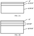
- the refractive index of the prepared buried silica layer is greater than that of the quartz substrate layer, and a structure formed by the quartz substrate and the buried silica layer is shown in FIG. 2A .
- a material other than quartz may also be used to prepare the substrate. If the material has a refractive index less than that of the buried silica layer, the single silica-layer structure shown in FIG. 2A may be used; if the material has a refractive index greater than that of the buried silica layer, the double silica-layer structure shown in FIG. 2B may be used, in which a refractive index of a lower buried oxide layer is less than that of an upper buried oxide layer.
- the lower buried oxide layer may serve as a buffer layer between the upper buried oxide layer and the high-refractive-index substrate, so that a refractive index of a silica layer close to the first lithium niobate thin film waveguide 6 and the second lithium niobate thin film waveguide 6' is greater than that of a silica layer away from the first lithium niobate thin film waveguide 6 and the second lithium niobate thin film waveguide 6'.
- a lithium niobate thin film layer 6" is firstly bonded on the buried silica layer (including the first buried silica layer 5, the second buried silica layer 5', and the third buried silica layer 5") through a special process, as shown in FIG. 2A and FIG. 2B .
- the quartz substrate layer, the buried silica layer and the lithium niobate thin film layer constitute an initial base, in which the quartz substrate layer is a lowermost layer of the initial base material, the buried silica layer is an intermediate layer of the initial base material, and the lithium niobate thin film layer is an uppermost layer of the initial base material.
- the first preset shape may include, but is not limited to a Mach-Zehnder interference type structure and a micro-ring coupler type structure.
- a cross-sectional dimension of the first lithium niobate thin film waveguide 6 is on the order of square microns.
- the Mach-Zehnder interference type structure is a strip structure shown in FIG. 3A and FIG. 3B , and a waveguide of this shape is a cuboid waveguide.
- the micro-ring coupler type structure is a ridge structure shown in FIG. 3C and FIG. 3D , and a waveguide of this shape is a cuboid waveguide on a substrate.
- the lithium niobate thin film layer 6" on the second buried silica layer 5' may be photoetched into a tapered optical waveguide structure to form the second lithium niobate thin film waveguide 6'.
- the tapered structure may have an end with a larger cross-sectional area connected to the first lithium niobate thin film waveguide 6 and an end with a smaller area located in a direction away from the first lithium niobate thin film waveguide 6, and the tapered structure is preferably a quadrangular pyramid.
- a method of etching the lithium niobate thin film layer 6" may be, for example, a dry etching, preferably a plasma-enhanced reactive ion etching.
- An etching gas may be fluorinebased or chlorine-based gas, which may include but is not limited to CF 4 , CHF 3 , SF 6 , Cl 2 , BCl 3 , Ar, O 2 , etc. It may be understood that the method of etching the lithium niobate thin film layer 6" is not limited to the above-mentioned dry etching.
- a width and a height of the cuboid waveguide are preferably within a range of 0.5 ⁇ m to 2 ⁇ m, and a vertical distance between an end face of the quadrangular pyramid waveguide close to the silica waveguide and an end face of the quadrangular pyramid waveguide away from the silica waveguide is preferably 200 ⁇ m, so that a light field may slowly transition from the first lithium niobate thin film waveguide 6 to the silica waveguide 12. It may be understood that a value range of the width and the height of the cuboid waveguide is not limited to 0.5 ⁇ m to 2 ⁇ m, and a selection of the vertical distance between the two end faces is not limited to 200 ⁇ m.
- a metal electrode 7 is prepared on both sides of the first lithium niobate thin film waveguide 6.
- a first cladding silica layer 8 is prepared on the first buried silica layer 5
- a second cladding silica layer 8' is prepared on the second lithium niobate thin film waveguide 6'
- a silica waveguide 12 is prepared on the third buried silica layer 5".
- a cladding silica layer with high refractive index may be prepared by doping a deposition process gas or adjusting a deposition process gas ratio during a deposition process.
- the wavelength-division multiplexer region formed after the deposition of the cladding silica layer is shown in FIG. 6
- the first light coupling structure formed after the deposition of the cladding silica layer is shown in FIG. 7A and FIG. 7B .
- a plasma-enhanced chemical vapor deposition process may be used to form the cladding silica layer.
- Silica may be generated by a reaction of silane and nitric oxide at 350 °C, and a reaction equation is SiH 4 (gaseous) + 2N 2 O (gaseous) -- SiO 2 (solid) + 2N 2 (gaseous) + 2H 2 (gaseous).
- the cladding silica layer meeting the above-mentioned refractive index requirement may be obtained by adjusting a ratio of SiH 4 to 2N 2 O, or may be obtained by doping.
- a planarization processing needs to be performed on the deposited silica, for example, using a chemical mechanical polishing.
- the planarized cladding silica layer on the surface of the first buried silica layer 5, the surface of the first lithium niobate thin film waveguide 6 and the surface of the metal electrode 7 may be etched to form a through hole, so that the first cladding silica layer 8 is obtained, as shown in FIG. 8A and FIG. 8B .
- a process of etching the cladding silica layer specifically includes: applying a photoresist on the cladding silica layer, exposing and developing using a mask, transferring a mask pattern to the photoresist, and then transferring the photoresist pattern to the cladding silica layer by etching.
- a gas mixture of CF 4 and H 2 may be selected as an etching gas for silica, and a content of H 2 in the gas mixture may be 50% of a volume of the gas mixture, a selection ratio of the CF 4 /H 2 gas mixture of this composition to silica and silicon may exceed 40:1, and the etching selectivity is good.
- a terminal resistor 9 and a metal lead wire 10 are prepared on the first cladding silica layer 8 and connected to the metal electrode 7 through the through hole in the first cladding silica layer 8.
- a metal may be deposited in the through hole of the first cladding silica layer 8 and a part of a surface of the first cladding silica layer 8 to prepare the terminal resistor 9 and the metal lead wire 10, as shown in FIG. 11A and FIG. 11B .
- the metal lead wire 10 may be prepared by using a physical vapor deposition method, and the metal lead wire 10 may contain aluminum or other conductive materials.
- a metal and titanium nitride may be deposited on a part of the surface of the upper layer of the first cladding silica layer 8, then the deposited metal and titanium nitride may be photoetched or peeled off into the terminal resistor 9 using a pattern transfer method (such as photoetching or peeling off), and a metal may be deposited in the through hole to electrically connect the terminal resistor 9 in the upper layer and the metal electrode 7 in the lower layer.
- the terminal resistor 9 is a terminal load resistor of a lithium niobate thin film modulator transmission line, and an electrode and resistor structure may be optimized to achieve the impedance matching of the two so as to improve a modulation efficiency of the lithium niobate thin film modulator. It may be understood that a material of the terminal resistor 9 may include but not be limited to titanium nitride.
- the top silica layer is prepared on the exposed surface of the prepared device.
- the top silica layer includes the first top silica layer 11, the second top silica layer 11' and the third top silica layer 11" described above, and the refractive index of the top silica layer is less than that of the buried silica layer and the cladding silica layer.
- the top silica layer may be prepared by a deposition process, and the top silica layer with low refractive index may be prepared by doping a deposition process gas or adjusting a deposition process gas ratio during the deposition process.
- first top silica layer 11 needs to be etched to form a metal pad.
- the second top silica layer 11' and the third top silica layer 11" do not need to be etched.
- the lithium niobate thin film modulator formed after operation S7 is shown in FIG. 12A and FIG. 12B
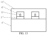
- the first optical coupling structure formed after operation S7 is shown in FIG. 13 .
- an alignment of a single-mode optical fiber and the silica waveguide may be achieved by etching a V-shaped groove on the base material.
- the optical fiber may be placed in the V-shaped groove, and after an alignment, the single-mode optical fiber and the silica waveguide may be fixed with a cover plate and an adhesive.
Landscapes
- Physics & Mathematics (AREA)
- General Physics & Mathematics (AREA)
- Optics & Photonics (AREA)
- Engineering & Computer Science (AREA)
- Nonlinear Science (AREA)
- Microelectronics & Electronic Packaging (AREA)
- Power Engineering (AREA)
- Chemical & Material Sciences (AREA)
- Ceramic Engineering (AREA)
- Crystallography & Structural Chemistry (AREA)
- Optical Integrated Circuits (AREA)
- Optical Modulation, Optical Deflection, Nonlinear Optics, Optical Demodulation, Optical Logic Elements (AREA)
Claims (8)
- Photonischer Chip, umfassend ein Lithiumniobatdünnschicht-Modulatorarray (1), ein erstes optische Koppelarray (2) und einen Silika-Wellenleiter-Wellenlängenmultiplexer (3), wobeidas Lithiumniobatdünnschicht-Modulatorarray (1) einen oder mehrere Lithiumniobatdünnschicht-Modulatoren umfasst und ausgebildet ist, ein optisches Signal zu modulieren;das erste optische Koppelarray (2) eine oder mehrere erste optische Koppelstrukturen umfasst, wobei ein Ende der ersten optischen Koppelstruktur mit einem zugeordneten Lithiumniobatdünnschicht-Modulator verbunden ist und das andere Ende mit dem Silika-Wellenleiter-Wellenlängenmultiplexer (3) verbunden ist, um das modulierte optische Signal an den Silika-Wellenleiter-Wellenlängenmultiplexer (3) zu übertragen; undder Silika-Wellenleiter-Wellenlängenmultiplexer (3) so konfiguriert ist, dass er Wellenlängenmultiplexing an dem modulierten optischen Signal durchführt,wobei der Lithiumniobatdünnschicht-Modulator umfasst:ein erstes Substrat (4);eine erste eingebettete Silikaschicht (5), die auf dem ersten Substrat (4) angeordnet ist;einen ersten Lithiumniobatdünnschicht-Wellenleiter (6), der auf der ersten eingebetteten Silikaschicht (5) in einer ersten vorbestimmten Form angeordnet ist;eine Metallelektrode (7), die auf beiden Seiten der ersten Lithiumniobatdünnschicht-Wellenleiterschicht (6) angeordnet ist;eine erste Silika-Mantelschicht (8), die die erste eingebettete Silikaschicht (5), den ersten Lithiumniobatdünnschicht-Wellenleiter (6) und die Metallelektrode (7) bedeckt, wobei die erste Silika-Mantelschicht (8) mit einem Durchgangsloch versehen ist, um die Metallelektrode (7) freizulegen;einen Abschlusswiderstand (9), der über das Durchgangsloch mit der Metallelektrode (7) verbunden ist;eine metallische Anschlussleitung (10), die mit der Metallelektrode (7) durch das Durchgangsloch verbunden ist; undeine erste obere Silikaschicht (11), die die erste Silika-Mantelschicht (8) und den Abschlusswiderstand (9) bedeckt,wobei die erste optische Kopplungsstruktur umfasst:ein zweites Substrat (4');eine zweite eingebettete Silikaschicht (5'), die auf dem zweiten Substrat (4') angeordnet ist;einen zweiten Lithiumniobatdünnschicht-Wellenleiter (6'), der auf der zweiten eingebetteten Silikaschicht (5') angeordnet ist, wobei der zweite Lithiumniobatdünnschicht-Wellenleiter (6') als eine sich verjüngende Struktur geformt ist, die ein Ende mit einer größeren Querschnittsfläche, das mit dem ersten Lithiumniobatdünnschicht-Wellenleiter (6) verbunden ist, und ein Ende mit einer kleineren Querschnittsfläche aufweist, das mit dem Silika-Wellenleiter-Wellenlängenmultiplexer (3) verbunden ist;eine zweite Silika-Mantelschicht (8'), die die zweite eingebettete Silikaschicht (5') und den zweiten Lithiumniobatdünnschicht-Wellenleiter (6') bedeckt; undeine zweite obere Silikaschicht (11'), die die zweite Silika-Mantelschicht (8') bedeckt.
- Photonischer Chip nach Anspruch 1, wobei der Silika-Wellenleiter-Wellenlängenmultiplexer (3) umfasst:ein drittes Substrat (4");eine dritte eingebettete Silikaschicht (5"), die auf dem dritten Substrat (4") angeordnet ist;einen Silika-Wellenleiter (12), der auf der dritten eingebetteten Silikaschicht (5") in einer zweiten vorbestimmten Form angeordnet ist und mit dem Ende mit der kleineren Querschnittsfläche des zweiten Lithiumniobatdünnschicht-Wellenleiters (6') verbunden ist; undeine dritte obere Silikaschicht (11"), die den Silika-Wellenleiter (12) bedeckt.
- Photonischer Chip nach Anspruch 2, wobei die erste eingebettete Silikaschicht (5), die zweite eingebettete Silikaschicht (5') oder die dritte eingebettete Silikaschicht (5") eine Silika-Einzelschicht mit einem Brechungsindex ist, der größer ist als der des ersten Substrats (4), des zweiten Substrats (4') oder des dritten Substrats (4"); oder
die erste eingebettete Silikaschicht (5), die zweite eingebettete Silikaschicht (5') oder die dritte eingebettete Silikaschicht (5") eine Silika-Doppelschicht mit einem Brechungsindex ist, der kleiner ist als der des ersten Substrats (4), des zweiten Substrats (4') oder des dritten Substrats (4"), und eine untere Silikaschicht in der Silika-Doppelschicht einen Brechungsindex hat, der kleiner ist als der einer oberen Silikaschicht in der Silika-Doppelschicht. - Photonischer Chip nach Anspruch 2, wobei eine Differenz zwischen einem Brechungsindex der ersten Silika-Mantelschicht (8), der zweiten Silika-Mantelschicht (8') oder des Silika-Wellenleiters (12) und einem Brechungsindex der ersten eingebetteten Silikaschicht (5), der zweiten eingebetteten Silikaschicht (5') oder der dritten eingebetteten Silikaschicht (5") kleiner als ein erster vorbestimmter Wert ist.
- Photonischer Chip nach Anspruch 2, wobei eine Differenz zwischen einem Brechungsindex der ersten oberen Silikaschicht (11), der zweiten oberen Silikaschicht (11') sowie der dritten oberen Silikaschicht (11") und einem Brechungsindex des ersten Substrats (4), des zweiten Substrats (4') sowie des dritten Substrats (4") kleiner als ein zweiter vorbestimmter Wert ist.
- Photonischer Chip nach Anspruch 2, wobei eine Differenz zwischen einem Brechungsindex der ersten eingebetteten Silikaschicht (5), der zweiten eingebetteten Silikaschicht (5') oder der dritten eingebetteten Silikaschicht (5") und einem Brechungsindex des ersten Substrats (4), des zweiten Substrats (4') sowie des dritten Substrats (4") größer als ein dritter vorbestimmter Wert ist, und eine Differenz zwischen einem Brechungsindex der ersten Silika-Mantelschicht (8), der zweiten Silika-Mantelschicht (8') oder des Silika-Wellenleiters (12) und einem Brechungsindex der ersten oberen Silikaschicht (11), der zweiten oberen Silikaschicht (11') sowie der dritten oberen Silikaschicht (11") größer ist als der dritte vorbestimmte Wert.
- Verfahren zum Herstellen des photonischen Chips gemäß den Ansprüchen 1 bis 6, umfassend:S1 Herstellen eines Substrats, umfassend ein erstes Substrat (4), ein zweites Substrat (4') und ein drittes Substrat (4");S2 Herstellen einer eingebetteten Silikaschicht auf dem Substrat, wobei die eingebettete Silikaschicht eine erste eingebettete Silikaschicht (5), eine zweite eingebettete Silikaschicht (5') und eine dritte eingebettete Silikaschicht (5") umfasst;S3 Herstellen eines ersten Lithiumniobatdünnschicht-Wellenleiters (6) auf der ersten eingebetteten Silikaschicht (5) und Herstellen eines sich verjüngenden zweiten Lithiumniobatdünnschicht-Wellenleiters (6') auf der zweiten eingebetteten Silikaschicht (5');S4 Herstellen einer Metallelektrode (7) auf beiden Seiten des ersten Lithiumniobatdünnschicht-Wellenleiters (6);S5 Herstellen einer ersten Silika-Mantelschicht (8) auf der ersten eingebetteten Silikaschicht (5), dem ersten Lithiumniobatdünnschicht-Wellenleiter (6) und der Metallelektrode (7), Herstellen einer zweiten Silika-Mantelschicht (8') auf dem zweiten Lithiumniobatdünnschicht-Wellenleiter (6') und Herstellen eines Silika-Wellenleiters (12) auf der dritten eingebetteten Silikaschicht (5");S6 Herstellen eines Abschlusswiderstands (9) und einer metallischen Anschlussleitung (10) auf der ersten Silika-Mantelschicht (8) und Verbinden des Abschlusswiderstands (9) und der metallischen Anschlussleitung (10) mit der Metallelektrode (7) durch ein Durchgangsloch in der ersten Silika-Mantelschicht (8);S7 Herstellen einer ersten oberen Silikaschicht (11) auf der ersten Silika-Mantelschicht (8) und dem Abschlusswiderstand (9), Herstellen einer zweiten oberen Silikaschicht (11') auf der zweiten Silika-Mantelschicht (8') und Herstellen einer dritten oberen Silikaschicht (11") auf dem Silika-Wellenleiter (12).
- Verfahren zum Herstellen des photonischen Chips gemäß Anspruch 7, wobei der zweite Lithiumniobatdünnschicht-Wellenleiter (6') ein Ende mit einer größeren Querschnittsfläche, das mit dem ersten Lithiumniobatdünnschicht-Wellenleiter (6) verbunden ist, und ein Ende mit einer kleineren Querschnittsfläche aufweist, das mit dem Silika-Wellenleiter (12) verbunden ist.
Applications Claiming Priority (1)
| Application Number | Priority Date | Filing Date | Title |
|---|---|---|---|
| PCT/CN2019/096361 WO2021007806A1 (zh) | 2019-07-17 | 2019-07-17 | 一种光子芯片及其制备方法 |
Publications (3)
| Publication Number | Publication Date |
|---|---|
| EP4001977A1 EP4001977A1 (de) | 2022-05-25 |
| EP4001977A4 EP4001977A4 (de) | 2023-03-29 |
| EP4001977B1 true EP4001977B1 (de) | 2025-04-16 |
Family
ID=74210128
Family Applications (1)
| Application Number | Title | Priority Date | Filing Date |
|---|---|---|---|
| EP19938090.8A Active EP4001977B1 (de) | 2019-07-17 | 2019-07-17 | Fotonischer chip und verfahren zu dessen herstellung |
Country Status (4)
| Country | Link |
|---|---|
| US (1) | US11874497B2 (de) |
| EP (1) | EP4001977B1 (de) |
| JP (1) | JP7417320B2 (de) |
| WO (1) | WO2021007806A1 (de) |
Families Citing this family (9)
| Publication number | Priority date | Publication date | Assignee | Title |
|---|---|---|---|---|
| CN111522154B (zh) * | 2020-05-14 | 2025-07-08 | 上海徕刻科技有限公司 | 一种弱相位漂移的铌酸锂波导 |
| JP7553003B2 (ja) * | 2020-05-30 | 2024-09-18 | 華為技術有限公司 | 電気光変調器、光チップ及び集積チップ |
| CN115145063A (zh) * | 2021-03-30 | 2022-10-04 | Tdk株式会社 | 光学器件 |
| WO2022235509A1 (en) * | 2021-05-01 | 2022-11-10 | Optonet Inc. | Highly-integrated compact diffraction-grating based semiconductor laser |
| CN115394873B (zh) * | 2022-08-24 | 2025-02-14 | 东南大学 | 一种黑磷薄膜铌酸锂探测器 |
| CN115440760B (zh) * | 2022-09-21 | 2024-08-06 | 武汉光谷信息光电子创新中心有限公司 | 半导体结构及其制作方法 |
| CN116047666A (zh) * | 2022-11-28 | 2023-05-02 | 浙江大学 | 在薄膜铌酸锂平台可拓展任意通道波分复用调制器阵列 |
| CN119812931B (zh) * | 2024-12-26 | 2025-11-14 | 广州光电存算芯片融合创新中心 | 一种c波段硅基异质集成的光发射器件及其制备方法 |
| CN119511600B (zh) * | 2025-01-15 | 2025-03-25 | 华南理工大学 | 一种铌酸锂光子芯片的混合存算架构及其实现方法 |
Family Cites Families (28)
| Publication number | Priority date | Publication date | Assignee | Title |
|---|---|---|---|---|
| JP2002116419A (ja) * | 2000-10-06 | 2002-04-19 | Nippon Telegr & Teleph Corp <Ntt> | 光変調装置及びその製造方法 |
| US7116851B2 (en) | 2001-10-09 | 2006-10-03 | Infinera Corporation | Optical signal receiver, an associated photonic integrated circuit (RxPIC), and method improving performance |
| US9372306B1 (en) | 2001-10-09 | 2016-06-21 | Infinera Corporation | Method of achieving acceptable performance in and fabrication of a monolithic photonic integrated circuit (PIC) with integrated arrays of laser sources and modulators employing an extended identical active layer (EIAL) |
| EP1436870A2 (de) * | 2001-10-09 | 2004-07-14 | Infinera Corporation | Integrierte fotonische sendschaltung und optisches netzwerk damit |
| DE10201103B4 (de) * | 2002-01-09 | 2004-05-13 | Infineon Technologies Ag | Optoelektronisches Bauelement |
| US7257283B1 (en) | 2006-06-30 | 2007-08-14 | Intel Corporation | Transmitter-receiver with integrated modulator array and hybrid bonded multi-wavelength laser array |
| US8050525B2 (en) * | 2006-10-11 | 2011-11-01 | Futurewei Technologies, Inc. | Method and system for grating taps for monitoring a DWDM transmitter array integrated on a PLC platform |
| CN101960345B (zh) * | 2007-10-19 | 2013-01-02 | 光导束公司 | 用于模拟应用的硅基光调制器 |
| US20090324163A1 (en) | 2008-06-30 | 2009-12-31 | Jds Uniphase Corporation | High confinement waveguide on an electro-optic substrate |
| CN101604074A (zh) | 2009-07-27 | 2009-12-16 | 浙江大学 | 一种双参数可调式波道间隔器芯片 |
| CN102055584B (zh) | 2009-10-28 | 2012-12-12 | 中国科学院半导体研究所 | 一种光纤保密通信装置及其数据加密方法 |
| JP5488226B2 (ja) | 2010-06-10 | 2014-05-14 | 富士通オプティカルコンポーネンツ株式会社 | マッハツェンダ型の光変調器 |
| CN102164017B (zh) | 2011-03-21 | 2013-09-18 | 中国科学院半导体研究所 | 四路并行数字调制和正交复用的波导芯片结构 |
| US20140079351A1 (en) * | 2012-09-20 | 2014-03-20 | Phase Sensitive Innovations, Inc | Millimeter-wave electro-optic modulator |
| CN105593747B (zh) * | 2013-06-09 | 2019-07-05 | 光电网股份有限公司 | 超低电压宽调制带宽低光学损耗光学强度或相位调制器 |
| JP2015191068A (ja) * | 2014-03-27 | 2015-11-02 | 日本電気株式会社 | 光変調器の出力モニター方法および出力モニター装置 |
| CN104330940B (zh) * | 2014-11-04 | 2017-03-08 | 中国科学院半导体研究所 | 基于超宽带光频率梳产生奈奎斯特光脉冲的装置 |
| US9768901B2 (en) * | 2014-11-20 | 2017-09-19 | Kaiam Corp. | Planar lightwave circuit active connector |
| CN105068189B (zh) | 2015-08-31 | 2018-04-20 | 中国科学院半导体研究所 | InP基波分‑模分复用少模光通信光子集成发射芯片 |
| CN105044931B (zh) * | 2015-09-10 | 2018-10-09 | 中国科学院半导体研究所 | 硅基集成化的差分电光调制器及其制备方法 |
| CN108474911B (zh) * | 2015-12-10 | 2020-12-11 | 博创科技英国有限公司 | 具有组合式发射器及接收器组合件的光学收发器 |
| CN206133134U (zh) | 2016-10-18 | 2017-04-26 | 天津领芯科技发展有限公司 | 一种高调制效率的铌酸锂薄膜电光调制器 |
| CN108732795A (zh) * | 2017-04-14 | 2018-11-02 | 天津领芯科技发展有限公司 | 一种硅基铌酸锂高速光调制器及其制备方法 |
| CN106933001B (zh) | 2017-05-04 | 2019-04-19 | 上海交通大学 | 基于硅光集成的光子模数转换芯片 |
| CN109407208B (zh) * | 2018-12-13 | 2021-03-05 | 中国科学院半导体研究所 | 光耦合结构、系统及光耦合结构的制备方法 |
| US10727640B2 (en) | 2018-12-27 | 2020-07-28 | Intel Corporation | Multi-wavelength laser |
| CN109639359B (zh) | 2019-01-07 | 2021-10-08 | 上海交通大学 | 基于微环谐振器的光子神经网络卷积层芯片 |
| CN110012368B (zh) | 2019-03-27 | 2021-08-20 | 兰州大学 | 一种兼容波分复用信号的硅基集成化片上多模光交换系统 |
-
2019
- 2019-07-17 EP EP19938090.8A patent/EP4001977B1/de active Active
- 2019-07-17 JP JP2022503400A patent/JP7417320B2/ja active Active
- 2019-07-17 US US17/627,544 patent/US11874497B2/en active Active
- 2019-07-17 WO PCT/CN2019/096361 patent/WO2021007806A1/zh not_active Ceased
Also Published As
| Publication number | Publication date |
|---|---|
| EP4001977A1 (de) | 2022-05-25 |
| EP4001977A4 (de) | 2023-03-29 |
| JP7417320B2 (ja) | 2024-01-18 |
| WO2021007806A1 (zh) | 2021-01-21 |
| US11874497B2 (en) | 2024-01-16 |
| US20220260779A1 (en) | 2022-08-18 |
| JP2022541536A (ja) | 2022-09-26 |
Similar Documents
| Publication | Publication Date | Title |
|---|---|---|
| EP4001977B1 (de) | Fotonischer chip und verfahren zu dessen herstellung | |
| US9620931B2 (en) | Optical device, optical transmission device, optical reception device, hybrid laser and optical transmission apparatus | |
| US6665476B2 (en) | Wavelength selective optical add/drop multiplexer and method of manufacture | |
| EP3153899B1 (de) | Schema zur optischen kopplung | |
| US6411642B1 (en) | Techniques for fabricating and packaging multi-wavelength semiconductor laser array devices (chips) and their applications in system architectures | |
| US7738753B2 (en) | CMOS compatible integrated dielectric optical waveguide coupler and fabrication | |
| US6416575B2 (en) | Photonic crystal multilayer substrate and manufacturing method thereof | |
| EP1994653B1 (de) | Verfahren und system für integrierte dwdm-sender | |
| CN110221387B (zh) | 一种光子芯片及其制备方法 | |
| US8050525B2 (en) | Method and system for grating taps for monitoring a DWDM transmitter array integrated on a PLC platform | |
| US20200083668A1 (en) | Guide transition device with digital grating deflectors and method | |
| US20200088939A1 (en) | Guide transition device and method | |
| US11906781B2 (en) | End-face coupling structures underneath a photonic layer | |
| US20260063934A1 (en) | Lithium niobate on insulator (lnoi) vertically tapered optical waveguide and method of forming the same | |
| CN115576052A (zh) | 波导结构及其制造方法 | |
| JP2008046546A (ja) | 光送信器 | |
| US20260043973A1 (en) | Optical devices and methods of manufacture | |
| JP2004029359A (ja) | 光導波路構造及びその製造方法 | |
| JP2020091309A (ja) | 半導体装置およびその製造方法 | |
| JP2025128968A (ja) | 光導波路素子 | |
| WO2023084610A1 (ja) | 光モジュールおよびその作製方法 | |
| CN120709821A (zh) | 一种多波长集成光源系统及其制造方法 | |
| CN121254421A (zh) | 光学装置及其制造方法 | |
| KR20010010639A (ko) | 갈륨비소 기판을 사용한 광검출기가 집적된 폴리머 도파로열격자 파장 분할 광소자 및 그 제작방법 | |
| JP2002040273A (ja) | 光半導体装置及びその製造方法 |
Legal Events
| Date | Code | Title | Description |
|---|---|---|---|
| STAA | Information on the status of an ep patent application or granted ep patent |
Free format text: STATUS: THE INTERNATIONAL PUBLICATION HAS BEEN MADE |
|
| PUAI | Public reference made under article 153(3) epc to a published international application that has entered the european phase |
Free format text: ORIGINAL CODE: 0009012 |
|
| STAA | Information on the status of an ep patent application or granted ep patent |
Free format text: STATUS: REQUEST FOR EXAMINATION WAS MADE |
|
| 17P | Request for examination filed |
Effective date: 20220124 |
|
| AK | Designated contracting states |
Kind code of ref document: A1 Designated state(s): AL AT BE BG CH CY CZ DE DK EE ES FI FR GB GR HR HU IE IS IT LI LT LU LV MC MK MT NL NO PL PT RO RS SE SI SK SM TR |
|
| DAV | Request for validation of the european patent (deleted) | ||
| DAX | Request for extension of the european patent (deleted) | ||
| A4 | Supplementary search report drawn up and despatched |
Effective date: 20230301 |
|
| RIC1 | Information provided on ipc code assigned before grant |
Ipc: G02F 1/035 20060101ALI20230223BHEP Ipc: G02B 6/122 20060101ALI20230223BHEP Ipc: G02B 6/12 20060101AFI20230223BHEP |
|
| GRAP | Despatch of communication of intention to grant a patent |
Free format text: ORIGINAL CODE: EPIDOSNIGR1 |
|
| STAA | Information on the status of an ep patent application or granted ep patent |
Free format text: STATUS: GRANT OF PATENT IS INTENDED |
|
| INTG | Intention to grant announced |
Effective date: 20250130 |
|
| GRAS | Grant fee paid |
Free format text: ORIGINAL CODE: EPIDOSNIGR3 |
|
| GRAA | (expected) grant |
Free format text: ORIGINAL CODE: 0009210 |
|
| STAA | Information on the status of an ep patent application or granted ep patent |
Free format text: STATUS: THE PATENT HAS BEEN GRANTED |
|
| AK | Designated contracting states |
Kind code of ref document: B1 Designated state(s): AL AT BE BG CH CY CZ DE DK EE ES FI FR GB GR HR HU IE IS IT LI LT LU LV MC MK MT NL NO PL PT RO RS SE SI SK SM TR |
|
| REG | Reference to a national code |
Ref country code: GB Ref legal event code: FG4D |
|
| REG | Reference to a national code |
Ref country code: CH Ref legal event code: EP Ref country code: DE Ref legal event code: R096 Ref document number: 602019068886 Country of ref document: DE |
|
| REG | Reference to a national code |
Ref country code: IE Ref legal event code: FG4D |
|
| REG | Reference to a national code |
Ref country code: NL Ref legal event code: MP Effective date: 20250416 |
|
| PG25 | Lapsed in a contracting state [announced via postgrant information from national office to epo] |
Ref country code: NL Free format text: LAPSE BECAUSE OF FAILURE TO SUBMIT A TRANSLATION OF THE DESCRIPTION OR TO PAY THE FEE WITHIN THE PRESCRIBED TIME-LIMIT Effective date: 20250416 |
|
| REG | Reference to a national code |
Ref country code: AT Ref legal event code: MK05 Ref document number: 1786102 Country of ref document: AT Kind code of ref document: T Effective date: 20250416 |
|
| PG25 | Lapsed in a contracting state [announced via postgrant information from national office to epo] |
Ref country code: ES Free format text: LAPSE BECAUSE OF FAILURE TO SUBMIT A TRANSLATION OF THE DESCRIPTION OR TO PAY THE FEE WITHIN THE PRESCRIBED TIME-LIMIT Effective date: 20250416 Ref country code: PT Free format text: LAPSE BECAUSE OF FAILURE TO SUBMIT A TRANSLATION OF THE DESCRIPTION OR TO PAY THE FEE WITHIN THE PRESCRIBED TIME-LIMIT Effective date: 20250818 Ref country code: FI Free format text: LAPSE BECAUSE OF FAILURE TO SUBMIT A TRANSLATION OF THE DESCRIPTION OR TO PAY THE FEE WITHIN THE PRESCRIBED TIME-LIMIT Effective date: 20250416 |
|
| PGFP | Annual fee paid to national office [announced via postgrant information from national office to epo] |
Ref country code: DE Payment date: 20250722 Year of fee payment: 7 |
|
| REG | Reference to a national code |
Ref country code: LT Ref legal event code: MG9D |
|
| PG25 | Lapsed in a contracting state [announced via postgrant information from national office to epo] |
Ref country code: NO Free format text: LAPSE BECAUSE OF FAILURE TO SUBMIT A TRANSLATION OF THE DESCRIPTION OR TO PAY THE FEE WITHIN THE PRESCRIBED TIME-LIMIT Effective date: 20250716 Ref country code: GR Free format text: LAPSE BECAUSE OF FAILURE TO SUBMIT A TRANSLATION OF THE DESCRIPTION OR TO PAY THE FEE WITHIN THE PRESCRIBED TIME-LIMIT Effective date: 20250717 |
|
| PG25 | Lapsed in a contracting state [announced via postgrant information from national office to epo] |
Ref country code: PL Free format text: LAPSE BECAUSE OF FAILURE TO SUBMIT A TRANSLATION OF THE DESCRIPTION OR TO PAY THE FEE WITHIN THE PRESCRIBED TIME-LIMIT Effective date: 20250416 |
|
| PG25 | Lapsed in a contracting state [announced via postgrant information from national office to epo] |
Ref country code: BG Free format text: LAPSE BECAUSE OF FAILURE TO SUBMIT A TRANSLATION OF THE DESCRIPTION OR TO PAY THE FEE WITHIN THE PRESCRIBED TIME-LIMIT Effective date: 20250416 |
|
| PGFP | Annual fee paid to national office [announced via postgrant information from national office to epo] |
Ref country code: GB Payment date: 20250722 Year of fee payment: 7 |
|
| PG25 | Lapsed in a contracting state [announced via postgrant information from national office to epo] |
Ref country code: HR Free format text: LAPSE BECAUSE OF FAILURE TO SUBMIT A TRANSLATION OF THE DESCRIPTION OR TO PAY THE FEE WITHIN THE PRESCRIBED TIME-LIMIT Effective date: 20250416 |
|
| PG25 | Lapsed in a contracting state [announced via postgrant information from national office to epo] |
Ref country code: AT Free format text: LAPSE BECAUSE OF FAILURE TO SUBMIT A TRANSLATION OF THE DESCRIPTION OR TO PAY THE FEE WITHIN THE PRESCRIBED TIME-LIMIT Effective date: 20250416 |
|
| PGFP | Annual fee paid to national office [announced via postgrant information from national office to epo] |
Ref country code: FR Payment date: 20250725 Year of fee payment: 7 |
|
| PG25 | Lapsed in a contracting state [announced via postgrant information from national office to epo] |
Ref country code: RS Free format text: LAPSE BECAUSE OF FAILURE TO SUBMIT A TRANSLATION OF THE DESCRIPTION OR TO PAY THE FEE WITHIN THE PRESCRIBED TIME-LIMIT Effective date: 20250716 |
|
| PG25 | Lapsed in a contracting state [announced via postgrant information from national office to epo] |
Ref country code: IS Free format text: LAPSE BECAUSE OF FAILURE TO SUBMIT A TRANSLATION OF THE DESCRIPTION OR TO PAY THE FEE WITHIN THE PRESCRIBED TIME-LIMIT Effective date: 20250816 |
|
| PG25 | Lapsed in a contracting state [announced via postgrant information from national office to epo] |
Ref country code: LV Free format text: LAPSE BECAUSE OF FAILURE TO SUBMIT A TRANSLATION OF THE DESCRIPTION OR TO PAY THE FEE WITHIN THE PRESCRIBED TIME-LIMIT Effective date: 20250416 |
|
| PG25 | Lapsed in a contracting state [announced via postgrant information from national office to epo] |
Ref country code: DK Free format text: LAPSE BECAUSE OF FAILURE TO SUBMIT A TRANSLATION OF THE DESCRIPTION OR TO PAY THE FEE WITHIN THE PRESCRIBED TIME-LIMIT Effective date: 20250416 Ref country code: SM Free format text: LAPSE BECAUSE OF FAILURE TO SUBMIT A TRANSLATION OF THE DESCRIPTION OR TO PAY THE FEE WITHIN THE PRESCRIBED TIME-LIMIT Effective date: 20250416 |
|
| REG | Reference to a national code |
Ref country code: DE Ref legal event code: R097 Ref document number: 602019068886 Country of ref document: DE |
|
| PG25 | Lapsed in a contracting state [announced via postgrant information from national office to epo] |
Ref country code: CZ Free format text: LAPSE BECAUSE OF FAILURE TO SUBMIT A TRANSLATION OF THE DESCRIPTION OR TO PAY THE FEE WITHIN THE PRESCRIBED TIME-LIMIT Effective date: 20250416 |
|
| PG25 | Lapsed in a contracting state [announced via postgrant information from national office to epo] |
Ref country code: EE Free format text: LAPSE BECAUSE OF FAILURE TO SUBMIT A TRANSLATION OF THE DESCRIPTION OR TO PAY THE FEE WITHIN THE PRESCRIBED TIME-LIMIT Effective date: 20250416 |
|
| PG25 | Lapsed in a contracting state [announced via postgrant information from national office to epo] |
Ref country code: RO Free format text: LAPSE BECAUSE OF FAILURE TO SUBMIT A TRANSLATION OF THE DESCRIPTION OR TO PAY THE FEE WITHIN THE PRESCRIBED TIME-LIMIT Effective date: 20250416 Ref country code: SK Free format text: LAPSE BECAUSE OF FAILURE TO SUBMIT A TRANSLATION OF THE DESCRIPTION OR TO PAY THE FEE WITHIN THE PRESCRIBED TIME-LIMIT Effective date: 20250416 |
|
| PG25 | Lapsed in a contracting state [announced via postgrant information from national office to epo] |
Ref country code: IT Free format text: LAPSE BECAUSE OF FAILURE TO SUBMIT A TRANSLATION OF THE DESCRIPTION OR TO PAY THE FEE WITHIN THE PRESCRIBED TIME-LIMIT Effective date: 20250416 |
|
| PLBE | No opposition filed within time limit |
Free format text: ORIGINAL CODE: 0009261 |
|
| STAA | Information on the status of an ep patent application or granted ep patent |
Free format text: STATUS: NO OPPOSITION FILED WITHIN TIME LIMIT |
|
| REG | Reference to a national code |
Ref country code: CH Ref legal event code: H13 Free format text: ST27 STATUS EVENT CODE: U-0-0-H10-H13 (AS PROVIDED BY THE NATIONAL OFFICE) Effective date: 20260224 |
|
| REG | Reference to a national code |
Ref country code: CH Ref legal event code: L10 Free format text: ST27 STATUS EVENT CODE: U-0-0-L10-L00 (AS PROVIDED BY THE NATIONAL OFFICE) Effective date: 20260225 |
|
| PG25 | Lapsed in a contracting state [announced via postgrant information from national office to epo] |
Ref country code: LU Free format text: LAPSE BECAUSE OF NON-PAYMENT OF DUE FEES Effective date: 20250717 |
|
| 26N | No opposition filed |
Effective date: 20260119 |