EP4002081A1 - Lese-schreib-umwandlungsschaltung und speicher - Google Patents
Lese-schreib-umwandlungsschaltung und speicher Download PDFInfo
- Publication number
- EP4002081A1 EP4002081A1 EP21818317.6A EP21818317A EP4002081A1 EP 4002081 A1 EP4002081 A1 EP 4002081A1 EP 21818317 A EP21818317 A EP 21818317A EP 4002081 A1 EP4002081 A1 EP 4002081A1
- Authority
- EP
- European Patent Office
- Prior art keywords
- read
- write
- local
- data line
- nmos transistor
- Prior art date
- Legal status (The legal status is an assumption and is not a legal conclusion. Google has not performed a legal analysis and makes no representation as to the accuracy of the status listed.)
- Ceased
Links
Images


Classifications
-
- G—PHYSICS
- G06—COMPUTING OR CALCULATING; COUNTING
- G06F—ELECTRIC DIGITAL DATA PROCESSING
- G06F3/00—Input arrangements for transferring data to be processed into a form capable of being handled by the computer; Output arrangements for transferring data from processing unit to output unit, e.g. interface arrangements
- G06F3/06—Digital input from, or digital output to, record carriers, e.g. RAID, emulated record carriers or networked record carriers
- G06F3/0601—Interfaces specially adapted for storage systems
- G06F3/0602—Interfaces specially adapted for storage systems specifically adapted to achieve a particular effect
- G06F3/061—Improving I/O performance
-
- G—PHYSICS
- G11—INFORMATION STORAGE
- G11C—STATIC STORES
- G11C7/00—Arrangements for writing information into, or reading information out from, a digital store
- G11C7/10—Input/output [I/O] data interface arrangements, e.g. I/O data control circuits, I/O data buffers
- G11C7/1078—Data input circuits, e.g. write amplifiers, data input buffers, data input registers, data input level conversion circuits
- G11C7/1096—Write circuits, e.g. I/O line write drivers
-
- G—PHYSICS
- G06—COMPUTING OR CALCULATING; COUNTING
- G06F—ELECTRIC DIGITAL DATA PROCESSING
- G06F3/00—Input arrangements for transferring data to be processed into a form capable of being handled by the computer; Output arrangements for transferring data from processing unit to output unit, e.g. interface arrangements
- G06F3/06—Digital input from, or digital output to, record carriers, e.g. RAID, emulated record carriers or networked record carriers
- G06F3/0601—Interfaces specially adapted for storage systems
- G06F3/0628—Interfaces specially adapted for storage systems making use of a particular technique
- G06F3/0655—Vertical data movement, i.e. input-output transfer; data movement between one or more hosts and one or more storage devices
- G06F3/0658—Controller construction arrangements
-
- G—PHYSICS
- G11—INFORMATION STORAGE
- G11C—STATIC STORES
- G11C11/00—Digital stores characterised by the use of particular electric or magnetic storage elements; Storage elements therefor
- G11C11/21—Digital stores characterised by the use of particular electric or magnetic storage elements; Storage elements therefor using electric elements
- G11C11/34—Digital stores characterised by the use of particular electric or magnetic storage elements; Storage elements therefor using electric elements using semiconductor devices
- G11C11/40—Digital stores characterised by the use of particular electric or magnetic storage elements; Storage elements therefor using electric elements using semiconductor devices using transistors
- G11C11/401—Digital stores characterised by the use of particular electric or magnetic storage elements; Storage elements therefor using electric elements using semiconductor devices using transistors forming cells needing refreshing or charge regeneration, i.e. dynamic cells
- G11C11/4063—Auxiliary circuits, e.g. for addressing, decoding, driving, writing, sensing or timing
- G11C11/407—Auxiliary circuits, e.g. for addressing, decoding, driving, writing, sensing or timing for memory cells of the field-effect type
- G11C11/4076—Timing circuits
-
- G—PHYSICS
- G11—INFORMATION STORAGE
- G11C—STATIC STORES
- G11C11/00—Digital stores characterised by the use of particular electric or magnetic storage elements; Storage elements therefor
- G11C11/21—Digital stores characterised by the use of particular electric or magnetic storage elements; Storage elements therefor using electric elements
- G11C11/34—Digital stores characterised by the use of particular electric or magnetic storage elements; Storage elements therefor using electric elements using semiconductor devices
- G11C11/40—Digital stores characterised by the use of particular electric or magnetic storage elements; Storage elements therefor using electric elements using semiconductor devices using transistors
- G11C11/401—Digital stores characterised by the use of particular electric or magnetic storage elements; Storage elements therefor using electric elements using semiconductor devices using transistors forming cells needing refreshing or charge regeneration, i.e. dynamic cells
- G11C11/4063—Auxiliary circuits, e.g. for addressing, decoding, driving, writing, sensing or timing
- G11C11/407—Auxiliary circuits, e.g. for addressing, decoding, driving, writing, sensing or timing for memory cells of the field-effect type
- G11C11/409—Read-write [R-W] circuits
- G11C11/4096—Input/output [I/O] data management or control circuits, e.g. reading or writing circuits, I/O drivers or bit-line switches
-
- G—PHYSICS
- G11—INFORMATION STORAGE
- G11C—STATIC STORES
- G11C16/00—Erasable programmable read-only memories
- G11C16/02—Erasable programmable read-only memories electrically programmable
- G11C16/06—Auxiliary circuits, e.g. for writing into memory
- G11C16/26—Sensing or reading circuits; Data output circuits
-
- G—PHYSICS
- G11—INFORMATION STORAGE
- G11C—STATIC STORES
- G11C5/00—Details of stores covered by group G11C11/00
- G11C5/14—Power supply arrangements, e.g. power down, chip selection or deselection, layout of wirings or power grids, or multiple supply levels
-
- G—PHYSICS
- G11—INFORMATION STORAGE
- G11C—STATIC STORES
- G11C7/00—Arrangements for writing information into, or reading information out from, a digital store
- G11C7/06—Sense amplifiers; Associated circuits, e.g. timing or triggering circuits
-
- G—PHYSICS
- G11—INFORMATION STORAGE
- G11C—STATIC STORES
- G11C7/00—Arrangements for writing information into, or reading information out from, a digital store
- G11C7/10—Input/output [I/O] data interface arrangements, e.g. I/O data control circuits, I/O data buffers
- G11C7/1048—Data bus control circuits, e.g. precharging, presetting, equalising
-
- G—PHYSICS
- G11—INFORMATION STORAGE
- G11C—STATIC STORES
- G11C7/00—Arrangements for writing information into, or reading information out from, a digital store
- G11C7/10—Input/output [I/O] data interface arrangements, e.g. I/O data control circuits, I/O data buffers
- G11C7/1051—Data output circuits, e.g. read-out amplifiers, data output buffers, data output registers, data output level conversion circuits
- G11C7/1063—Control signal output circuits, e.g. status or busy flags, feedback command signals
-
- G—PHYSICS
- G11—INFORMATION STORAGE
- G11C—STATIC STORES
- G11C7/00—Arrangements for writing information into, or reading information out from, a digital store
- G11C7/10—Input/output [I/O] data interface arrangements, e.g. I/O data control circuits, I/O data buffers
- G11C7/1051—Data output circuits, e.g. read-out amplifiers, data output buffers, data output registers, data output level conversion circuits
- G11C7/1069—I/O lines read out arrangements
-
- G—PHYSICS
- G11—INFORMATION STORAGE
- G11C—STATIC STORES
- G11C7/00—Arrangements for writing information into, or reading information out from, a digital store
- G11C7/10—Input/output [I/O] data interface arrangements, e.g. I/O data control circuits, I/O data buffers
- G11C7/1078—Data input circuits, e.g. write amplifiers, data input buffers, data input registers, data input level conversion circuits
- G11C7/109—Control signal input circuits
-
- G—PHYSICS
- G11—INFORMATION STORAGE
- G11C—STATIC STORES
- G11C7/00—Arrangements for writing information into, or reading information out from, a digital store
- G11C7/12—Bit line control circuits, e.g. drivers, boosters, pull-up circuits, pull-down circuits, precharging circuits, equalising circuits, for bit lines
-
- G—PHYSICS
- G11—INFORMATION STORAGE
- G11C—STATIC STORES
- G11C7/00—Arrangements for writing information into, or reading information out from, a digital store
- G11C7/22—Read-write [R-W] timing or clocking circuits; Read-write [R-W] control signal generators or management
-
- G—PHYSICS
- G06—COMPUTING OR CALCULATING; COUNTING
- G06F—ELECTRIC DIGITAL DATA PROCESSING
- G06F2212/00—Indexing scheme relating to accessing, addressing or allocation within memory systems or architectures
- G06F2212/10—Providing a specific technical effect
- G06F2212/1016—Performance improvement
- G06F2212/1024—Latency reduction
-
- G—PHYSICS
- G11—INFORMATION STORAGE
- G11C—STATIC STORES
- G11C11/00—Digital stores characterised by the use of particular electric or magnetic storage elements; Storage elements therefor
- G11C11/21—Digital stores characterised by the use of particular electric or magnetic storage elements; Storage elements therefor using electric elements
- G11C11/34—Digital stores characterised by the use of particular electric or magnetic storage elements; Storage elements therefor using electric elements using semiconductor devices
- G11C11/40—Digital stores characterised by the use of particular electric or magnetic storage elements; Storage elements therefor using electric elements using semiconductor devices using transistors
- G11C11/401—Digital stores characterised by the use of particular electric or magnetic storage elements; Storage elements therefor using electric elements using semiconductor devices using transistors forming cells needing refreshing or charge regeneration, i.e. dynamic cells
- G11C11/4063—Auxiliary circuits, e.g. for addressing, decoding, driving, writing, sensing or timing
- G11C11/407—Auxiliary circuits, e.g. for addressing, decoding, driving, writing, sensing or timing for memory cells of the field-effect type
- G11C11/409—Read-write [R-W] circuits
- G11C11/4094—Bit-line management or control circuits
-
- G—PHYSICS
- G11—INFORMATION STORAGE
- G11C—STATIC STORES
- G11C2207/00—Indexing scheme relating to arrangements for writing information into, or reading information out from, a digital store
- G11C2207/22—Control and timing of internal memory operations
- G11C2207/2281—Timing of a read operation
-
- G—PHYSICS
- G11—INFORMATION STORAGE
- G11C—STATIC STORES
- G11C2207/00—Indexing scheme relating to arrangements for writing information into, or reading information out from, a digital store
- G11C2207/22—Control and timing of internal memory operations
- G11C2207/229—Timing of a write operation
Definitions
- Embodiments of the disclosure relate to the technical field of semiconductors, and particularly to a read-write conversion circuit and a memory.
- a Dynamic Random Access Memory is a common semiconductor storage device in computers, and is composed of multiple repeated storage units.
- Each storage unit typically includes a capacitor and a transistor.
- the transistor includes a gate connected to a word line, a drain connected to a bitline, and a source connected to the capacitor.
- a voltage signal on the word line can turn the transistor on or off to read data information stored in the capacitor through the bitline or write data information into the capacitor for storage through the bitline.
- DRAM can be classified as a Double Data Rate (DDR) DRAM, a Graphics Double Data Rate (GDDR) DRAM, or a Low Power Double Data Rate (LPDDR) DRAM.
- DDR Double Data Rate
- GDDR Graphics Double Data Rate
- LPDDR Low Power Double Data Rate
- the embodiments of the disclosure are intended to provide a read-write conversion circuit and a memory as a solution to the technical problem.
- the read-write operation speed of the read-write conversion circuit is variable, so that the performance of the memory is improved.
- the embodiments of the disclosure provide a read-write conversion circuit, which is characterized by that the circuit includes: a read-write conversion module, performing a read-write operation in response to a read-write control signal; and a control module, outputting a variable read-write control signal in response to a read-write speed configuration signal to control the speed of the read-write operation of the read-write conversion module to be variable.
- a speed configuration module may further be included, which may be connected with the control module and configured to output the read-write speed configuration signal to the control module.
- the read-write control signal may include a read control signal and a write control signal.
- the read-write conversion module may perform a read operation in response to the read control signal, and perform a write operation in response to the write control signal.
- the speed configuration module may include: a read speed configuration unit, configured to output a read speed configuration signal in the read-write speed configuration signal to the control module, which causes the control module to output the variable read control signal in response to the read speed configuration signal, controlling the speed of the read operation to be variable.
- the speed configuration module may also include a write speed configuration unit, configured to output a write speed configuration signal in the read-write speed configuration signal to the control module to cause the control module to output the variable write control signal in response to the read speed configuration signal to control a speed of the write operation to be variable.
- a write speed configuration unit configured to output a write speed configuration signal in the read-write speed configuration signal to the control module to cause the control module to output the variable write control signal in response to the read speed configuration signal to control a speed of the write operation to be variable.
- a local data line, a local complementary data line, and a global data line may further be included.
- data transmission may be performed between each of the local data line, the local complementary data line, and the global data line, in which the data signals of the local data line and the local complementary data line may be opposite in phase.
- the read-write conversion module may include a local read-write unit, performing a local read-write operation in response to a local read-write control signal in the read-write control signal.
- the control module may include a local control unit, outputting the variable local read-write control signal in response to a local read-write speed configuration signal in the read-write speed configuration signal, in order to control the speed of the local read-write operation of the local read-write unit to be variable.
- the read-write conversion circuit may further include a local speed configuration module, connected with the local control unit and configured to output the local read-write speed configuration signal to the local control unit.
- the read-write conversion circuit may further include a sense amplifier, connected with the local read-write unit through the local data line and the local complementary data line, and configured to sense the voltage of the bit line.
- the same local read-write unit may be connected with multiple sense amplifiers through the local data line and the local complementary data line.
- a write data path may be as follows: from the local read-write unit to the sense amplifier via the local data line and the local complementary data line, and then to the bit line via the sense amplifier.
- a read data path may be as follows: from the bit line to the local data line and the local complementary data line via the sense amplifier, and then to the local read-write unit via the local data line and the local complementary data line.
- the read-write conversion module may include a global read-write unit, performing a global read-write operation in response to a global read-write control signal in the read-write control signal.
- the control module may include a global control unit, outputting the variable global read-write control signal in response to a global read-write speed configuration signal in the read-write speed configuration signal to control a speed of the global read-write operation of the global read-write unit to be variable.
- the read-write conversion circuit may further include a global speed configuration module, connected with the global control unit and configured to output the global read-write speed configuration signal to the global control unit.
- the local read-write unit may include a local amplifier, connected between the local data line and the local complementary data line and configured to amplify the data of the local data line and the data of the local complementary data line.
- the local amplifier may include: a first phase inverter, a first input end of the first phase inverter being electrically connected with the local data line, and a first output end of the first phase inverter being electrically connected with the local complementary data line; and a second phase inverter, a second input terminal of the second phase inverter being electrically connected with the first output terminal of the first phase inverter and the local complementary data line, and a second output terminal of the second phase inverter being electrically connected with the first input terminal of the first phase inverter and the local data line.
- the first phase inverter may include a first P-channel Metal Oxide Semiconductor (PMOS) transistor and a first N-channel Metal Oxide Semiconductor (NMOS) transistor.
- a gate of the first PMOS transistor may be connected with a gate of the first NMOS transistor to serve as the first input terminal of the first phase inverter
- a source of the first PMOS transistor may be connected with working power
- a drain of the first PMOS transistor may be connected with a drain of the first NMOS transistor to serve as the first output terminal of the first phase inverter.
- the second phase inverter may include a zeroth PMOS transistor and a zeroth NMOS transistor.
- a gate of the zeroth PMOS transistor may be connected with a gate of the zeroth NMOS transistor to serve as the second input terminal of the second phase inverter.
- a source of the zeroth PMOS transistor may be connected with the working power, and a drain of the zeroth PMOS transistor may be connected with a drain of the zeroth NMOS transistor to serve as the second output terminal of the second phase inverter.
- the local read-write unit may include a local read conversion circuit, configured to transmit the data of the local data line and the local complementary data line to the global data line in response to a local read control signal in the local read-write control signal.
- the local read conversion circuit may include a third NMOS transistor and a fourth NMOS transistor. A drain of the third NMOS transistor may be connected with the global data line, a gate of the third NMOS transistor may be connected with the local complementary data line, and a source of the third NMOS transistor may be connected with a drain of the fourth NMOS transistor. A gate of the fourth NMOS transistor may receive a local read signal in the local read control signal, while a source may be grounded.
- the read-write conversion circuit may further include a global complementary data line, and during the read operation, data signals of the global complementary data line and the global data line may be opposite in phase.
- the local read conversion circuit may further include an eighth NMOS transistor and a ninth NMOS transistor. A drain of the eighth NMOS transistor may be connected with the global complementary data line, a gate of the eighth NMOS transistor may be connected with the local data line, and a source of the eighth NMOS transistor may be connected with a drain of the ninth NMOS transistor. A gate of the ninth NMOS transistor may receive the local read signal, while a source may be grounded.
- the local read-write unit may include a local write conversion circuit, configured to transmit data of the global data line to the local data line and the local complementary data line in response to a local write control signal in the local read-write control signal.
- the local write conversion circuit may include a fifth NMOS transistor, a sixth NMOS transistor, and a seventh NMOS transistor.
- a drain of the fifth NMOS transistor may be connected with the local complementary data line
- a gate of the fifth NMOS transistor may be connected with a source of the seventh NMOS transistor
- a source of the fifth NMOS transistor may be connected with a drain of the sixth NMOS transistor.
- a gate of the sixth NMOS transistor may receive a local write signal in the local write control signal, while a source may be grounded.
- a drain of the seventh NMOS transistor may be connected with the local data line, while a gate may receive the local write signal.
- the read-write conversion circuit may further include the global complementary data line, and during the read-write operation, the data signals of the global complementary data line and the global data line may be opposite in phase.
- the local write conversion circuit may further include a tenth NMOS transistor, an eleventh NMOS transistor, and a twelfth NMOS transistor.
- a drain of the tenth NMOS transistor may be connected with the local data line
- a gate of the tenth NMOS transistor may be connected with a source of the twelfth NMOS transistor and the global complementary data line
- a source of the tenth NMOS transistor may be connected with a drain of the eleventh NMOS transistor.
- a gate of the eleventh NMOS transistor may receive the local write signal, while a source may be grounded.
- a drain of the twelfth NMOS transistor may be connected with the local complementary data line, while a gate may receive the local write signal.
- the local read-write unit may further include a precharging circuit, connected between the local data line and the local complementary data line and configured to precharge the local data line and the local complementary data line in response to a precharging control signal.
- a precharging circuit connected between the local data line and the local complementary data line and configured to precharge the local data line and the local complementary data line in response to a precharging control signal.
- the precharging circuit may include a third PMOS transistor, a fourth PMOS transistor, and a fifth PMOS transistor.
- a gate of the third PMOS transistor, a gate of the fourth PMOS transistor, and a gate of the fifth PMOS transistor may receive the precharging control signal.
- a source of the third PMOS transistor and a source of the fourth PMOS transistor may be connected with working power.
- a drain of the third PMOS transistor may be electrically connected with the local data line.
- a drain of the fourth PMOS transistor may be electrically connected with the local complementary data line.
- the fifth PMOS transistor may be electrically connected with the local data line and the local complementary data line in response to the precharging control signal.
- the embodiments of the disclosure also provide a memory, which may include the abovementioned read-write conversion circuit.
- the embodiments of the disclosure provide the read-write conversion circuit with high structural performance, which includes the read-write conversion module that performs the read-write operation in response to the read-write control signal and a control module that outputs the variable read-write control signal in response to the read-write speed configuration signal, so that the speed of the read-write operation of the read-write conversion module remains variable. Since the read-write control signal output by the control module is variable, the speed of the read-write operation performed by the read-write conversion module after receiving the variable read-write control signal is also variable, and the speed of the read-write operation of the read-write conversion circuit can therefore be configured.
- the read-write conversion circuit provided in the embodiments of the disclosure may adjust the speed of the read-write operation as practically required, so that the read-write conversion circuit may be applied more extensively, not only to a low-speed read-write operation but also to a high-speed read-write operation, for example.
- the high-speed read-write operation may be adjusted to the low-speed read-write operation when not required, so that the problem of high power consumption caused by the high-speed read-write operation is resolved. Therefore, the performance of the read-write conversion circuit provided in the embodiments of the disclosure may be improved.
- the read-write conversion module includes the local read-write unit
- the control module includes the local control unit, outputting the variable local read-write control signal in response to the local read-write speed configuration signal in the read-write speed configuration signal so that the speed of the local read-write operation of the local read-write unit remains variable. Therefore, the speed of the local read-write operation of the read-write conversion circuit provided in the embodiments of the disclosure may be configured.
- the read-write conversion module includes the global read-write unit
- the control module includes the global control unit, outputting the variable global read-write control signal in response to the global read-write speed configuration signal in the read-write speed configuration signal so that the speed of the global read-write operation of the global read-write unit remains variable. Therefore, the speed of the global read-write operation of the read-write conversion circuit provided in the embodiments of the disclosure may be configured.
- the local read-write unit includes the local amplifier, connected between the local data line and the local complementary data line and configured to amplify the data of the local data line and the data of the local complementary data line.
- the local amplifier is favorable for accelerating the distinction between the local data line and the local complementary data line, and is favorable not only for increasing the speed of the local read-write operation but also for reducing the drive requirement of the local data line and the local complementary data line on the sense amplifier, thereby reducing the difficulty of designing sense amplifiers.
- a speed (including a read speed and a write speed) of a read-write operation thereof is fixed. Since of the speed of the read-write operation of the DRAM is fixed, if the DRAM is designed to have a fixed low read-write operation speed, it is difficult to meet the demand of the DRAM on a high read-write operation speed in some periods. On the other hand, if the DRAM is designed to have a fixed high read-write operation speed, then for the periods where the DRAM has low speeds of read-write operations, the fixed high read-write speed of the DRAM will cause an energy consumption issue. That is, at present, the memory faces a problem of fixed read-write operation speed and high power consumption.
- the embodiments of the disclosure provide a read-write conversion circuit, which includes a read-write conversion module and a control module.
- the control module outputs a variable read-write control signal in response to a read-write speed configuration signal to control a speed of a read-write operation of the read-write conversion module to be variable. Therefore, according to the embodiments of the disclosure, the speed of the read-write operation may be configured to adjust the speed of the read-write operation of the read-write conversion circuit to an expected speed, avoiding unnecessary power consumption of the read-write conversion circuit and improving the performance of the read-write conversion circuit.
- FIG. 1 is a schematic diagram of a read-write conversion circuit according to an embodiment of the disclosure.
- the read-write conversion circuit includes: a read-write conversion module 101, performing a read-write operation in response to a read-write control signal; and a control module 102, outputting a variable read-write control signal in response to a read-write speed configuration signal to control a speed of the read-write operation of the read-write conversion module 101 to be variable.
- the read-write conversion circuit may further include a local data line Ldat, a local complementary data line Ldat#, and a global data line Gdat.
- a local data line Ldat a local complementary data line Ldat#
- a global data line Gdat a global data line Gdat.
- data signals read or written by the read-write conversion circuit are paired.
- Each pair of data signals include two pieces of data.
- one of the two pieces of data is a high-level signal, while the other piece of data is a low-level signal. Therefore, the read-write conversion circuit includes at least one pair of local data line Ldat and local complementary data line Ldat#, and the two pieces of data are the data of the local data line Ldat and the data of the local complementary data line Ldat#, respectively.
- data is transmitted from the local data line Ldat and the local complementary data line Ldat# to the global data line Gdat; and during a write operation of the read-write conversion circuit, data is transmitted from the global data line Gdat to the local data line Ldat and the local complementary data line Ldat#.
- the local data line Ldat is also called a local data line
- the local complementary data line Ldat# is also called a local complementary data line
- the global data line Gdat is also called a global data line.
- a single-end transmission manner is used for the global data line Gdat of the read-write conversion circuit, namely no global complementary data line complementary with the global data line Gdat in data signal phase is arranged in the read-write conversion circuit.
- a double-end transmission manner may also be used for the global data line of the read-write conversion circuit, namely the read-write conversion circuit may further include a global complementary data line, and during the read-write operation, the data signal of the global complementary data line and the data signal of the global data line are opposite in phase.
- the read-write conversion circuit is applied to a memory.
- the memory includes a column selection module 100 and multiple storage units.
- the local data line Ldat is connected with a bit line BL through the column selection module 100
- the local complementary data line Ldat# is connected with a complementary bit line BL# through the column selection module 100.
- the storage unit for the read operation or the write operation is selected through the column selection module 100.
- signals are transmitted between the bit line BL connected with the selected storage unit and the local data line Ldat, and signals are transmitted between the complementary bit line BL# connected with the selected storage unit and the local complementary data line Ldat#.
- the read-write conversion module 101 transmits the data of the local data line Ldat and the data of the local complementary data line Ldat# to the global data line Gdat; and during the write operation, the read-write conversion module 101 transmits data of the global data line Gdat to the local data line Ldat and the local complementary data line Ldat#.
- the read-write control signal includes a column selection signal, a local read-write control signal, and a global read-write control signal.
- the local read-write control signal is configured to control the read-write conversion module 101 to perform a local read-write operation.
- the global read-write control signal is configured to control the read-write conversion module 101 to perform a global read-write operation.
- the rate of the read-write control signal influences the speed of the read-write operation of the read-write conversion circuit. For example, if the rate of the read-write control signal is higher, the speed of the read-write operation is correspondingly higher; and if the rate of the read-write control signal is lower, the speed of the read-write operation is correspondingly lower.
- the read-write control signal is provided by the control module 102, and the read-write control signal output by the control module 102 is variable, specifically, the rate of the read-write control signal is variable.
- the read-write speed configuration signal is related to an expected speed of the read-write operation. When the speed of the read-write operation is not the expected speed, the read-write control signal output by the control module 102 changes. That is, the rate of the read-write control signal changes, which changes the speed of the read-write operation performed by the read-write conversion module 101 in response to the changed read-write control signal, therefore ensuring that the read-write speed of the read-write operation is the expected speed.
- the control module 102 when the speed of a read-write operation performed by the read-write conversion module 101 in response to a first read-write control signal is lower than the expected speed, the control module 102 outputs a second read-write control signal in response to the read-write speed configuration signal to increase the speed of the read-write operation of the read-write conversion module 101 to the expected speed.
- the control module 102 outputs a fourth read-write control signal in response to the read-write speed configuration signal to decrease the speed of the read-write operation of the read-write conversion module 101 to the expected speed.
- the speed of the read-write operation of the read-write conversion module 101 is variable, the speed of the read-write operation of the read-write conversion module 101 may be adjusted according to a practical performance requirement. For example, an increase or decrease in the speed of data transmission in the read-write operation can be used to meet different read-write performance requirements and reduce unnecessary power consumption as well.
- the read-write conversion circuit may further include a speed configuration module 103, connected with the control module 102 and configured to output a read-write speed configuration signal to the control module 102.
- the speed configuration module 103 is integrated into the read-write conversion circuit to help to shorten the transmission path for transmitting the read-write speed configuration signal to the control module 102 and to accelerate a response speed of the control module 102 for a more timely output of the adjusted read-write control signal so that changing the speed of the read-write operation of the read-write conversion module 101 may be achieved more rapidly.
- the read-write control signal includes a read control signal and a write control signal.
- the read-write conversion module 101 performs the read operation in response to the read control signal, and performs the write operation in response to the write control signal.
- the control module 102 outputs a variable read control signal in response to the read-write speed configuration signal to control the speed of the read operation of the read-write conversion module 101 to be variable.
- the control module 102 also outputs a variable write control signal in response to the read-write speed configuration signal to control the speed of the write operation of the read-write conversion module 101 to be variable.
- the read-write speed configuration signal includes a read speed configuration signal and a write speed configuration signal.
- the speed configuration module 103 includes: a read speed configuration unit 113, configured to output a read speed configuration signal in the read-write speed configuration signal to the control module 102, which then outputs a variable read control signal in response to the read speed configuration signal to control the speed of the read operation to be variable; and a write speed configuration unit 123, configured to output a write speed configuration signal in the read-write speed configuration signal to the control module 102, which then outputs a variable write control signal in response to the read speed configuration signal to control the speed of the write operation to be variable.
- the speed configuration module may further include a local speed configuration module and a global speed configuration module.
- the local speed configuration module is configured to output a local read speed configuration signal to the control module to control a speed of the local read-write operation of the read-write conversion module to be variable.
- the global speed configuration module is configured to output a global read-write speed configuration signal to the control module to control a speed of the global read-write operation of the read-write conversion module to be variable.
- the speed configuration module may also be provided by another circuit except the read-write conversion circuit.
- the control module 102 outputs the variable read-write control signal to make variable the speed of the read-write operation of the read-write conversion module 101.
- This allows for the read-write conversion circuit to be applied to more scenarios, for example, applied not only to a high-speed read-write operation but also to a low-speed read-write operation. Moreover, it resolves the problem of high power consumption caused by a sustained high-speed read-write operation state.
- Another embodiment of the disclosure also provides a read-write conversion circuit.
- the read-write conversion circuit is substantially the same as the read-write conversion circuit provided in the previous embodiment. The difference is that the read-write conversion module and the control module are described in more detail in the embodiment.
- the read-write conversion circuit provided in the embodiment will be described below in detail in combination with the drawings. For the same or corresponding parts as the previous embodiment, one may refer to the detailed descriptions provided in the previous embodiment.
- FIG. 2 shows a read-write conversion circuit according to another embodiment of the disclosure.
- the read-write conversion circuit includes a local data line Ldat, a local complementary data line Ldat#, a global data line Gdat, a global complementary data line Gdat#, a read-write conversion module 201, and a control module 202.
- the read-write conversion module 201 performs a read-write operation in response to a read-write control signal to implement data transmission between each of the local data line Ldat and the local complementary data line Ldat#, and each of the global data line Gdat and the global complementary data line Gdat#.
- the data signals of the local data line Ldat and the local complementary data line Ldat# are opposite in phase
- the data signals of the global data line Gdat and the global complementary data line Gdat# are opposite in phase.
- the read-write conversion circuit may be provided with no global complementary data line, or provided only with the global data line.
- the read-write conversion circuit may be provided with no global complementary data line, or provided only with the global data line.
- the read-write conversion module 201 includes a local read-write unit 211, performing a local read-write operation in response to a local read-write control signal in the read-write control signal.
- the local read-write control signal includes a local read signal Rd and a local amplification enable signal.
- control module 202 includes a local control unit 212, outputting the variable local read-write control signal in response to a local read-write speed configuration signal in a read-write speed configuration signal to control the speed of the local read-write operation in the local read-write unit 211 to be variable.
- the speed of the local read-write operation in the read-write conversion circuit is variable.
- the speed of a local read operation in the local read-write operation is variable, and the speed of a local write operation in the local read-write operation is also variable.
- the local read operation may be changed from a high-speed read to a low-speed read, or, changed from a low-speed read to a high-speed read.
- the local write operation may be changed from a high-speed write to a low-speed write, or, changed from a low-speed write to a high-speed write. Since the speed of the local read-write operation is variable, the speed of the local read-write operation may be adjusted as practically necessary to meet the demands on the data transmission speed and simultaneously to ensure the advantage of low power consumption of the read-write conversion circuit.
- the read-write conversion circuit may further include a local speed configuration module 213, connected with the local control unit 212 and configured to output the local read-write speed configuration signal to the local control unit 212, so that the local read-write control signal output by the local control unit 212 is made adjustable.
- a local speed configuration module 213 connected with the local control unit 212 and configured to output the local read-write speed configuration signal to the local control unit 212, so that the local read-write control signal output by the local control unit 212 is made adjustable.
- the local read-write speed configuration signal may also be provided for the local control unit by an external circuit, that is, the read-write conversion circuit does not need the local speed configuration module.
- the read-write conversion circuit may further include a sense amplifier 214.
- the sense amplifier 214 is connected with the local read-write unit 211 through the local data line Ldat and the local complementary data line Ldat#, and is configured to sense voltages of the bit line BL and the complementary bit line BL#.
- bit line BL is connected with the local data line Ldat through the sense amplifier 214, and the complementary bit line BL# is connected with the local complementary data line Ldat# through the sense amplifier 214.
- the sense amplifier 214 receives a column selection signal CSL.
- the sense amplifier 214 includes two NMOS transistors (not marked), and gates of the NMOS transistors receive the column selection signal CSL.
- One NMOS transistor is connected with the bit line BL and the local data line Ldat in response to the column selection signal CSL, while the other NMOS transistor is connected with the complementary bit line BL# and the local complementary data line Ldat# in response to the column selection signal CSL.
- the NMOS transistor receives the column selection signal CSL and is turned on, the bit line BL is connected with the local data line Ldat, and the complementary bit line BL# is connected with the local complementary data line Ldat#.
- the NMOS transistor stops receiving the column selection signal CSL the bit line BL is disconnected from the local data line Ldat, and the complementary bit line BL# is disconnected from the local complementary data line Ldat#.
- the sense amplifier may include any number of transistors, for example, multiple NMOS transistors and/or multiple PMOS transistors. Any device capable of realizing a sense amplifier function may be used as the sense amplifier.
- the bit line BL is connected with a memory transistor (not marked).
- a gate of the memory transistor is connected with a word line WL.
- One end of the memory transistor is connected with the bit line BL, while the other end is connected with a voltage Vplate through a capacitor (not marked).
- the complementary bit line BL# is connected with a control transistor (not marked).
- One end of the control transistor is connected with the complementary bit line BL#, while the other end is connected with the voltage Vplate.
- the same local read-write unit 211 may be connected with multiple sense amplifiers 214 through the local data line Ldat and the local complementary data line Ldat#.
- FIG. 2 shows only one sense amplifier 214.
- the read-write conversion circuit is applied to a memory.
- a write data path goes from the local read-write unit 211 to the sense amplifier via the local data line Ldat and via the local complementary data line Ldat#, and then to the bit line BL and the complementary bit line BL# via the sense amplifier 214.
- a read data path goes from the bit line to the local data line Ldat and to the local complementary data line Ldat# via the sense amplifier 214, and then to the local read-write unit 211 via the local data line Ldat and via the local complementary data line Ldat#.
- the read-write conversion module 201 further includes a global read-write unit 221, performing a global read-write operation in response to a global read-write control signal in the read-write control signal.
- the control module 202 includes a global control unit 222, outputting the variable global read-write control signal in response to a global read-write speed configuration signal in the read-write speed configuration signal, in order to maintain a variable speed of the global read-write operation in the global read-write unit 221.
- the speed of the global read-write operation in the read-write conversion circuit is variable.
- the speed of a global read operation in the global read-write operation is variable, and the speed of a global write operation in the global read-write operation is variable.
- control module may include only one of the local control unit or the global control unit, and correspondingly, only the speed of the local read-write operation is variable or only the speed of the global read-write operation is variable.
- the read-write conversion circuit may further include a global speed configuration module 223, connected with the global control unit 222 and configured to output the global read-write speed configuration signal to the global control unit 222.
- a global speed configuration module 223 connected with the global control unit 222 and configured to output the global read-write speed configuration signal to the global control unit 222.
- the local speed configuration module 213 and the global speed configuration module 223 may be integrated into the same speed configuration module 203.
- the speed configuration module 203 is configured to output the local read-write speed configuration signal to the local control unit 212, and is further configured to output the global read-write speed configuration signal to the global control unit 222.
- the global read-write speed configuration signal may also be provided for the global control unit by an external circuit, that is, the read-write conversion circuit does not need the global speed configuration module.
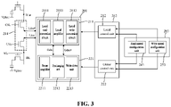
- FIG. 3 shows another read-write conversion circuit according to another embodiment.
- the read-write conversion circuit may further include a read speed configuration unit 243, configured to output a read speed configuration signal in the read-write speed configuration signal to the local control unit 212 and the global control unit 222.
- This causes the local control unit 212 to output a variable local read control signal in response to the read speed configuration signal to control the speed of the local read operation to be variable.
- this causes the global control unit 222 to output a variable global read control signal in response to the read speed configuration signal to control the speed of the global read operation to be variable.
- the read-write conversion circuit may further include a write speed configuration unit 253, configured to output a write speed configuration signal in the read-write speed configuration signal to the local control unit 212 and the global control unit 222, causing the local control unit 212 to output a variable local write control signal in response to the write speed configuration signal to control the speed of the local write operation to be variable.
- the read speed configuration unit 243 and the write speed configuration unit 253 may be integrated into the same speed configuration module 203. Descriptions about the speed configuration module 203 may be obtained by reference to the aforementioned embodiment.
- the write data path goes to the global data line Gdat and the global complementary data line Gdat# via the global read-write unit 221, then to the local read-write unit 211 via the global data line Gdat and the global complementary data line Gdat#, from the local read-write unit 211 to the sense amplifier 214 via the local data line Ldat and the local complementary data line Ldat#, and then to the bit line BL and the complementary bit line BL# via the sense amplifier 214.
- the read data path goes from the bit line BL and the complementary bit line BL# to the local data line Ldat and the local complementary data line Ldat# via the sense amplifier 214, then to the local read-write unit 211 via the local data line Ldat and the local complementary data line Ldat#, then to the global data line Gdat and the global complementary data line Gdat# via the local read-write unit 211, and finally to the global read-write unit 221 via the global data line Gdat and the global complementary data line Gdat#.
- the local read-write unit 211 includes a local read conversion circuit 2111 that is configured to transmit data of the local data line Ldat and the local complementary data line Ldat# to the global data line Gdat and the global complementary data line Gdat# in response to the local read control signal in the local read-write control signal.
- the control module 202 outputs the local read control signal and the variable local read control signal in response to the read-write speed configuration signal to adjust the read speed of the local read conversion circuit 2111, making the speed of the local read operation of the read-write conversion module 201 to be variable.
- the local read-write unit 211 further includes a local write conversion circuit 2112, configured to transmit data of the global data line Gdat and the global complementary data line Gdat# to the local data line Ldat and the local complementary data line Ldat# in response to the local write control signal in the local read-write control signal.
- a local write conversion circuit 2112 configured to transmit data of the global data line Gdat and the global complementary data line Gdat# to the local data line Ldat and the local complementary data line Ldat# in response to the local write control signal in the local read-write control signal.
- the control module 202 outputs the local write control signal, and the control module 202 outputs the variable local write control signal in response to the read-write speed configuration signal to adjust a write speed of the local write conversion circuit 2112 to further make variable the speed of the local write operation of the read-write conversion module 201.
- the local read-write unit 211 further includes a local amplifier 2113, connected between the local data line Ldat and the local complementary data line Ldat# and configured to amplify the data of the local data line Ldat and the data of the local complementary data line Ldat#.
- the control module 202 outputs the variable local read control signal or the local write control signal to make variable an amplification speed of the local amplifier 2113, so that the speeds of the local read operation and the local write operation of the read-write conversion module 201 may be changed to a certain extent.
- the local amplifier 2113 forms a circuit for amplifying the signal of the local data line Ldat and the signal of the local complementary data line Ldat#, and helps to accelerate the distinction between the level of the local data line Ldat and the level of the local complementary data line Ldat#, thereby increasing the data signal transmission speed and improving the data read-write speed.
- the local data line Ldat and the local complementary data line Ldat# have reduced demands on the drive capability of the sense amplifier in the memory.
- the sense amplifier has enough drive capability for the local data line Ldat and the local complementary data line Ldat# to satisfy the trend towards device miniaturization while simultaneously ensuring high electrical performance of the read-write conversion circuit, thereby improving the storage performance of the memory containing the read-write conversion circuit.
- the global read-write unit 221 includes a sense amplifier 2211, a precharging unit 2212, and a write drive unit 2213.
- the sense amplifier 2211 may amplify the data signal of the global data line Gdat and the data signal of the global complementary data line Gdat#.
- the precharging unit 2212 may precharge the global data line Gdat and the global complementary data line Gdat#.
- the control module 202 outputs the variable global read control signal to adjust the speed of the global read operation or the global write operation of the global read-write unit 221, such as adjusting the amplification speed of the sense amplifier 2211, the precharging speed of the precharging unit 2212, and the drive speed of the write drive unit 2213, to achieve the purpose of changing the global read-write operation of the read-write conversion module 201.
- the read-write conversion circuit may further include a precharging circuit 204.
- the precharging circuit 204 is connected between the local data line Ldat and the local complementary data line Ldat#, and is configured to precharge the local data line Ldat and the local complementary data line Ldat# in response to a precharging control signal.
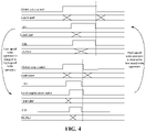
- FIG. 4 is a sequence diagram of a read-write control signal corresponding to a high-speed write operation and low-speed write operation in a write operation of the read-write conversion circuit according to the embodiment.
- FIG. 5 is a sequence diagram of a read-write control signal corresponding to a high-speed read operation and low-speed read operation in a read operation of the read-write conversion circuit according to the embodiment.
- FIG. 4 and FIG. 5 also show a bit line/complementary bit line signal (BL/BL#), a global data line/global complementary data line signal (Gdat/Gdat#), and a local data line/local complementary data line signal (Ldat/Ldat#). It can be understood that high speed and low speed are relative.
- BL/BL# bit line/complementary bit line signal
- Gdat/Gdat# global data line/global complementary data line signal
- Ldat/Ldat# local data line/local complementary data line signal
- the read-write control signal when the write operation is performed, includes the global write control signal, the column selection signal CSL, a local write signal Wr, and a local amplification enable. It can be understood that, when the low-speed write operation is performed, the level of local amplification enable may be 0, and thus the low-speed write operation corresponds to the sequence diagram that does not show the local amplification enable.
- FIG. 4 only shows a sequence diagram of each read-write control signal in a single clock period. From the whole clock period, when the low-speed write operation is changed to the high-speed write operation, the rate of the write control signal in the corresponding read-write control signal increases, and when the high-speed write operation is changed to the low-speed write operation, the rate of the write control signal in the corresponding read-write control signal decreases.
- the read-write control signal when the read operation is performed, includes the column selection signal CSL, a local read signal Rd, a global amplification enable, a global precharging signal, and a local amplification enable. It can be understood that, when the low-speed read operation is performed, the level of local amplification enable may be 0, and thus the low-speed read operation corresponds to the sequence diagram that does not show the local amplification enable. It is easily seen from FIG.
- the rate of the read-write control signal decreases, the data transmission rates of the local data line Ldat and the local complementary data line Ldat# decrease, and the data transmission rates of the global data line Gdat and the global complementary data line Gdat# decrease; and when the low-speed read operation is changed to the high-speed read operation, the rate of the read-write control signal increases, the data transmission rates of the local data line Ldat and the local complementary data line Ldat# increase, and the data transmission rates of the global data line Gdat and the global complementary data line Gdat# increase.
- FIG. 5 only shows a sequence diagram of each read-write control signal in a single clock period. From the whole clock period, when the low-speed read operation is changed to the high-speed write operation, the rate of the read control signal in the corresponding read-write control signal increases, and when the high-speed read operation is changed to the low-speed read operation, the rate of the read control signal in the corresponding read-write control signal decreases.
- FIG. 4 and FIG. 5 only show some common read-write control signals influencing the speed of the read-write operation, and there may be other read-write control signals influencing the speed of the read-write operation in practical circuits according to different circuit designs.
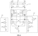
- FIG. 6 is a schematic diagram of a circuit structure of the local read-write unit in the read-write conversion circuit according to the embodiment.
- FIG. 7 is a schematic diagram of another circuit structure of the local read-write unit in the read-write conversion circuit according to the embodiment.
- the local read-write unit 211 includes the local read conversion circuit 2111, configured to transmit the data of the local data line Ldat and the local complementary data line Ldat# to the global data line Gdat, in response to the local read control signal in the local read-write control signal.
- the local read conversion circuit 2111 includes a third NMOS transistor MN3 and a fourth NMOS transistor MN4.
- the drain of the third NMOS transistor MN3 is connected with the global data line Gdat
- the gate of the third NMOS transistor MN3 is connected with the local complementary data line Ldat#
- the source of the third NMOS transistor MN3 is connected with the drain of the fourth NMOS transistor MN4.
- the gate of the fourth NMOS transistor MN4 receives the local read signal Rd in the local read control signal, while the source is grounded.
- the local read conversion circuit 2111 may also be another appropriate transformed circuit.
- the gate of the fourth MNOS transistor is connected with the local complementary data line, and the gate of the third NMOS transistor receives the local read signal.
- a double-end transmission manner may also be used for the global data line Gdat, namely that the read-write conversion circuit includes the global data line Gdat and the global complementary data line Gdat#.
- the data signals of the global complementary data line Gdat# and the global data line Gdat are opposite in phase.
- the local read conversion circuit 2111 further includes an eighth NMOS transistor MN8 and a ninth NMOS transistor MN9.
- the drain of the eighth NMOS transistor MN8 is connected with the global complementary data line Gdat#, the gate of the eighth NMOS transistor MN8 is connected with the local data line Ldat, and the source of the eighth NMOS transistor MN8 is connected with the drain of the ninth MNOS transistor MN9.
- the gate of the ninth NMOS transistor MN9 receives the local read signal Rd, while the source is grounded.
- the local read-write unit 211 includes the local write conversion circuit 2112, configured to transmit the data of the global data line Gdat to the local data line Ldat and the local complementary data line Ldat#, in response to the local write control signal in the local read-write control signal.
- the local write conversion circuit 2112 includes a fifth NMOS transistor MN5, a sixth NMOS transistor MN6, and a seventh NMOS transistor MN7.
- the drain of the fifth NMOS transistor MN5 is connected with the local complementary data line Ldat#
- the gate of the fifth NMOS transistor MN5 is connected with the source of the seventh NMOS transistor MN7
- the source of the fifth NMOS transistor MN5 is connected with the drain of the sixth NMOS transistor MN6.
- the gate of the sixth NMOS transistor MN6 receives the local write signal Wr in the local write control signal, while the source is grounded.
- the drain of the seventh NMOS transistor MN7 is connected with the local data line Ldat, while the gate receives the local write signal Wr.
- the read-write conversion circuit 211 further includes the global complementary data line Gdat#. During the read operation, the data signals of the global complementary data line Gdat# and the global data line Gdat are opposite in phase.
- the local write conversion circuit 2112 further includes a tenth NMOS transistor MN10, an eleventh NMOS transistor MN11, and a twelfth NMOS transistor MN12.
- the drain of the tenth NMOS transistor MN10 is connected with the local data line Ldat, the gate of the tenth NMOS transistor MN10 is connected with the source of the twelfth NMOS transistor MN12 and the global complementary data line Gdat#, and the source of the tenth NMOS transistor MN10 is connected with the drain of the eleventh NMOS transistor MN11.
- the gate of the eleventh NMOS transistor MN11 receives the local write signal Wr, while the source is grounded.
- the drain of the twelfth NMOS transistor MN12 is connected with the local complementary data line Ldat#, while the gate receives the local write signal Wr.
- the local amplifier 2113 includes: a first phase inverter 21, a first input end of the first phase inverter being electrically connected with the local data line Ldat, and a first output end out1 of the first phase inverter being electrically connected with the local complementary data line Ldat#; and a second phase inverter 22, a second input end in2 of the second phase inverter 22 being electrically connected with the second output end out2 of the first phase inverter 21 and the local complementary data line Ldat#, and a second output end out2 of the second phase inverter 22 being electrically connected with the first input end in1 of the first phase inverter 21 and the local data line Ldat.
- the first phase inverter 21 includes a first PMOS transistor MP1 and a first NMOS transistor MN1.
- the gate of the first PMOS transistor MP1 is electrically connected with the gate of the first NMOS transistor MN1 to serve as the first input end in1 of the first phase inverter
- the source of the first PMOS transistor MP1 is connected with working power VDD
- the drain of the first PMOS transistor MP1 is connected with the drain of the first NMOS transistor MN1 to serve as the first output end out1 of the first phase inverter 21.
- the second phase inverter 22 includes a zeroth PMOS transistor MP0 and a zeroth NMOS transistor MN0.
- a gate of the zeroth PMOS transistor MP0 is electrically connected with the gate of the zeroth NMOS transistor MN0 to serve as the second input end in2 of the second phase inverter 22, the source of the zeroth PMOS transistor MP0 is connected with the working power VDD, and the drain of the zeroth PMOS transistor MP0 is connected with the drain of the zeroth NMOS transistor MN0 to serve as the second output end out2 of the second phase inverter 22.
- the first PMOS transistor MP1, the first NMOS transistor MN1, the zeroth PMOS transistor MP0, and the zeroth NMOS transistor MN0 form the local amplifier 2113.
- the local amplifier 2113 further includes an enable NMOS transistor mn.
- the first phase inverter 21 and the second phase inverter 22 are also connected with a drain of the enable NMOS transistor mn.
- the drain of the enable NMOS transistor mn is grounded, while the gate receives the local enable signal En.
- the source of the first NMOS transistor MN1 is connected with the source of the zeroth NMOS transistor MN0 and the drain of the sixth NMOS transistor MN6. In some other embodiments, the source of the first NMOS transistor MN1 is grounded, and the source of the zeroth NMOS transistor MN0 is grounded.
- the speed of transmitting the data from the bit line BL to the local data line Ldat is increased, the speed of transmitting the data from the complementary bit line BL# to the local complementary data line Ldat# is increased, and the drive requirement of the memory on the sense amplifier is reduced.
- the arrangement of the local amplifier 2113 may pull the local complementary data line Ldat# with a lower voltage down to "0" more rapidly or pull the local data line Ldat with a higher voltage up to "1" more rapidly. Therefore, the speed to pull the local data line Ldat up is increased and the speed to pull the local complementary data line Ldat# down is also increased. Furthermore, the local data line Ldat and the local complementary data line Ldat# have reduced demands on the drive of the sense amplifier.
- the local data line Ldat and the local complementary data line Ldat# may reach high levels or low levels more rapidly, transmission from the local data line Ldat and the local complementary data line Ldat# to the global data line Gdat and the global complementary data line Gdat# may be implemented earlier. Therefore, when the data is read, the speed of data transmission from the local data line Ldat and the local complementary data line Ldat# to the global data line Gdat and the global complementary data line Gdat# is increased.
- the local amplifier 2113 may also amplify the local data line Ldat and the local complementary data line Ldat# to increase the speed of data transmission from the global data line Gdat and the global complementary data line Gdat# to the local data line Ldat and the local complementary data line Ldat#.
- the precharging circuit 204 includes a third PMOS transistor MP3, a fourth PMOS transistor MP4, and a fifth PMOS transistor MP5.
- the gate of the third PMOS transistor MP3, the gate of the fourth PMOS transistor MP4, and the gate of the fifth PMOS transistor MP5 receive the precharging control signal Eq.
- the source of the third PMOS transistor MP3 and the source of the fourth PMOS transistor MP4 are connected with the working power VDD, the drain of the third PMOS transistor MP3 is electrically connected with the local data line Ldat, and the drain of the fourth PMOS transistor MP4 is electrically connected with the local complementary data line Ldat#.
- the fifth PMOS transistor MP5 is electrically connected with the local data line Ldat and the local complementary data line Ldat# in response to the precharging control signal Eq.
- the control module 202 outputs the read-write control signal in response to the read-write speed configuration signal to change the data read rate of the local read conversion circuit 2111 or the local write conversion circuit 2112, etc., thereby adjusting the read-write operation speed of the read-write conversion circuit.
- the read-write conversion circuit provided in the embodiment may adjust not only the local read-write operation speed but also the global read-write operation speed, so that the convenience for adjusting the read-write operation speed of the read-write conversion circuit is further improved.
- an embodiment of the disclosure provides a memory, which includes the abovementioned read-write conversion circuit.
- the memory may be a DRAM, a Static Random-Access Memory (SRAM), a Magneto resistive Random-Access Memory (MRAM), a Ferroelectric Random-Access Memory (RAM) (FeRAM), a Phase Change RAM (PCRAM), a NAND flash memory, a NOR flash memory, or another memory.
- SRAM Static Random-Access Memory
- MRAM Magneto resistive Random-Access Memory
- FeRAM Ferroelectric Random-Access Memory
- PCRAM Phase Change RAM
- NAND flash memory a NOR flash memory, or another memory.
Landscapes
- Engineering & Computer Science (AREA)
- Theoretical Computer Science (AREA)
- Human Computer Interaction (AREA)
- Physics & Mathematics (AREA)
- General Engineering & Computer Science (AREA)
- General Physics & Mathematics (AREA)
- Microelectronics & Electronic Packaging (AREA)
- Computer Hardware Design (AREA)
- Power Engineering (AREA)
- Databases & Information Systems (AREA)
- Dram (AREA)
- Memory System (AREA)
Applications Claiming Priority (3)
| Application Number | Priority Date | Filing Date | Title |
|---|---|---|---|
| CN202021024456.9U CN212032138U (zh) | 2020-06-05 | 2020-06-05 | 读写转换电路以及存储器 |
| CN202010505672.3A CN113760174B (zh) | 2020-06-05 | 2020-06-05 | 读写转换电路以及存储器 |
| PCT/CN2021/074702 WO2021244055A1 (zh) | 2020-06-05 | 2021-02-01 | 读写转换电路以及存储器 |
Publications (2)
| Publication Number | Publication Date |
|---|---|
| EP4002081A1 true EP4002081A1 (de) | 2022-05-25 |
| EP4002081A4 EP4002081A4 (de) | 2022-10-19 |
Family
ID=78817831
Family Applications (1)
| Application Number | Title | Priority Date | Filing Date |
|---|---|---|---|
| EP21818317.6A Ceased EP4002081A4 (de) | 2020-06-05 | 2021-02-01 | Lese-schreib-umwandlungsschaltung und speicher |
Country Status (4)
| Country | Link |
|---|---|
| US (1) | US11783877B2 (de) |
| EP (1) | EP4002081A4 (de) |
| JP (1) | JP7352741B2 (de) |
| KR (1) | KR102865649B1 (de) |
Families Citing this family (2)
| Publication number | Priority date | Publication date | Assignee | Title |
|---|---|---|---|---|
| CN116486850B (zh) * | 2022-01-14 | 2025-07-11 | 长鑫存储技术有限公司 | 一种感应放大电路、方法和半导体存储器 |
| US12112791B2 (en) | 2022-01-14 | 2024-10-08 | Changxin Memory Technologies, Inc. | Sense amplifying circuit and method, and semiconductor memory |
Family Cites Families (17)
| Publication number | Priority date | Publication date | Assignee | Title |
|---|---|---|---|---|
| JPH05189976A (ja) | 1991-09-03 | 1993-07-30 | Seiko Epson Corp | 半導体装置及び電子機器 |
| US6212109B1 (en) * | 1999-02-13 | 2001-04-03 | Integrated Device Technology, Inc. | Dynamic memory array having write data applied to selected bit line sense amplifiers before sensing to write associated selected memory cells |
| DE19961518B4 (de) | 1999-12-20 | 2007-03-29 | Infineon Technologies Ag | Verfahren zum Betreiben eines Strom-Leseverstärkers |
| JP2002032985A (ja) | 2000-07-18 | 2002-01-31 | Mitsubishi Electric Corp | 半導体記憶装置 |
| DE10121837C1 (de) | 2001-05-04 | 2002-12-05 | Infineon Technologies Ag | Speicherschaltung mit mehreren Speicherbereichen |
| JP2004158050A (ja) * | 2002-11-01 | 2004-06-03 | Renesas Technology Corp | 半導体記憶装置 |
| US7203102B2 (en) | 2004-10-27 | 2007-04-10 | Infineon Technologies, Ag | Semiconductor memory having tri-state driver device |
| KR100689707B1 (ko) | 2004-11-12 | 2007-03-08 | 삼성전자주식회사 | 뱅크 선택신호 제어회로, 이를 포함하는 반도체 메모리 장치 및 뱅크 선택신호 제어방법 |
| US7227799B2 (en) | 2005-04-29 | 2007-06-05 | Infineon Technologies Ag | Sense amplifier for eliminating leakage current due to bit line shorts |
| DE102005045311B4 (de) | 2005-09-22 | 2007-05-10 | Infineon Technologies Ag | Halbleiterspeicher, insbesondere Halbleiterspeicher mit Leseverstärker und Bitleitungs-Schalter |
| DE102007007565A1 (de) | 2007-02-15 | 2008-08-21 | Qimonda Ag | Halbleiter-Speicherbauelement mit umschaltbarem Substratpotential, und Verfahren zum Betrieb eines Halbleiter-Speicherbauelements |
| KR20120111951A (ko) * | 2009-06-29 | 2012-10-11 | 모사이드 테크놀로지스 인코퍼레이티드 | 주파수 구성 가능 클록 도메인을 갖는 브릿징 장치 |
| US8817562B2 (en) * | 2012-07-31 | 2014-08-26 | Freescale Semiconductor, Inc. | Devices and methods for controlling memory cell pre-charge operations |
| CN103077740A (zh) | 2012-12-27 | 2013-05-01 | 北京大学 | 带补偿电路的电流模式灵敏放大器及使用方法 |
| CN110827891B (zh) | 2018-08-10 | 2021-08-03 | 北京百度网讯科技有限公司 | 信号转换单元、存储器以及应用于存储器的驱动方法 |
| CN110867203B (zh) | 2019-11-19 | 2021-12-14 | 上海华力微电子有限公司 | 存储器读取速度调节电路 |
| CN212032138U (zh) | 2020-06-05 | 2020-11-27 | 长鑫存储技术(上海)有限公司 | 读写转换电路以及存储器 |
-
2021
- 2021-02-01 KR KR1020227022256A patent/KR102865649B1/ko active Active
- 2021-02-01 EP EP21818317.6A patent/EP4002081A4/de not_active Ceased
- 2021-02-01 JP JP2022538927A patent/JP7352741B2/ja active Active
- 2021-08-22 US US17/445,604 patent/US11783877B2/en active Active
Also Published As
| Publication number | Publication date |
|---|---|
| JP2023509879A (ja) | 2023-03-10 |
| US20210383846A1 (en) | 2021-12-09 |
| KR102865649B1 (ko) | 2025-09-29 |
| US11783877B2 (en) | 2023-10-10 |
| JP7352741B2 (ja) | 2023-09-28 |
| KR20220101735A (ko) | 2022-07-19 |
| EP4002081A4 (de) | 2022-10-19 |
Similar Documents
| Publication | Publication Date | Title |
|---|---|---|
| US11315610B1 (en) | Sense amplifier, memory and method for controlling sense amplifier | |
| US8644101B2 (en) | Local sense amplifier circuit and semiconductor memory device including the same | |
| CN212032139U (zh) | 读写转换电路以及存储器 | |
| EP4020477B1 (de) | Lese-schreib-schalter und speicher | |
| CN113760174B (zh) | 读写转换电路以及存储器 | |
| CN212032138U (zh) | 读写转换电路以及存储器 | |
| KR101564340B1 (ko) | 개선된 안정성 및 감소된 비트셀 사이즈를 갖는 저전력 5t sram | |
| US7616511B2 (en) | Input/output line sense amplifier and semiconductor memory device using the same | |
| US9159401B2 (en) | Semiconductor device having hierarchical bit line structure | |
| US11887655B2 (en) | Sense amplifier, memory, and method for controlling sense amplifier by configuring structures using switches | |
| EP4027346A1 (de) | Integrierte schaltung | |
| US12080340B2 (en) | Control circuit, method for reading and writing and memory | |
| US11783877B2 (en) | Read-write conversion circuit and memory | |
| US8542547B2 (en) | Semiconductor device and data processing system | |
| WO2021244055A1 (zh) | 读写转换电路以及存储器 | |
| RU2797927C1 (ru) | Схема преобразования чтения-записи и память | |
| RU2797927C9 (ru) | Схема преобразования чтения-записи и память | |
| EP3971897B1 (de) | Integrierte halbleiterschaltung und speicher | |
| US7142465B2 (en) | Semiconductor memory | |
| KR20050038839A (ko) | 감지 증폭 입력 신호를 부스팅하여 데이터 독출 성능을개선한 반도체 메모리 장치의 입출력 라인 구동회로 및 그방법 | |
| KR20030083232A (ko) | 입출력 라인의 프리차지 전압을 하강시킬 수 있는 반도체메모리 장치 | |
| WO2014129576A1 (ja) | 半導体記憶装置 | |
| KR20120115859A (ko) | 센스앰프회로 및 이를 포함한 반도체 메모리 장치 |
Legal Events
| Date | Code | Title | Description |
|---|---|---|---|
| STAA | Information on the status of an ep patent application or granted ep patent |
Free format text: STATUS: THE INTERNATIONAL PUBLICATION HAS BEEN MADE |
|
| PUAI | Public reference made under article 153(3) epc to a published international application that has entered the european phase |
Free format text: ORIGINAL CODE: 0009012 |
|
| STAA | Information on the status of an ep patent application or granted ep patent |
Free format text: STATUS: REQUEST FOR EXAMINATION WAS MADE |
|
| 17P | Request for examination filed |
Effective date: 20220218 |
|
| AK | Designated contracting states |
Kind code of ref document: A1 Designated state(s): AL AT BE BG CH CY CZ DE DK EE ES FI FR GB GR HR HU IE IS IT LI LT LU LV MC MK MT NL NO PL PT RO RS SE SI SK SM TR |
|
| A4 | Supplementary search report drawn up and despatched |
Effective date: 20220919 |
|
| RIC1 | Information provided on ipc code assigned before grant |
Ipc: G11C 11/4096 20060101ALI20220913BHEP Ipc: G11C 11/4094 20060101ALI20220913BHEP Ipc: G11C 11/4076 20060101ALI20220913BHEP Ipc: G11C 7/22 20060101ALI20220913BHEP Ipc: G11C 7/10 20060101ALI20220913BHEP Ipc: G06F 3/06 20060101AFI20220913BHEP |
|
| STAA | Information on the status of an ep patent application or granted ep patent |
Free format text: STATUS: EXAMINATION IS IN PROGRESS |
|
| 17Q | First examination report despatched |
Effective date: 20230321 |
|
| DAV | Request for validation of the european patent (deleted) | ||
| DAX | Request for extension of the european patent (deleted) | ||
| REG | Reference to a national code |
Ref country code: DE Ref legal event code: R003 |
|
| STAA | Information on the status of an ep patent application or granted ep patent |
Free format text: STATUS: THE APPLICATION HAS BEEN REFUSED |
|
| 18R | Application refused |
Effective date: 20240301 |