EP4002433A1 - Schleuder-, spül- und trocknermodul mit verbesserten trocknungseigenschaften - Google Patents
Schleuder-, spül- und trocknermodul mit verbesserten trocknungseigenschaften Download PDFInfo
- Publication number
- EP4002433A1 EP4002433A1 EP21194938.3A EP21194938A EP4002433A1 EP 4002433 A1 EP4002433 A1 EP 4002433A1 EP 21194938 A EP21194938 A EP 21194938A EP 4002433 A1 EP4002433 A1 EP 4002433A1
- Authority
- EP
- European Patent Office
- Prior art keywords
- rotatable member
- rotatable
- substrate
- spin rinse
- rinse dryer
- Prior art date
- Legal status (The legal status is an assumption and is not a legal conclusion. Google has not performed a legal analysis and makes no representation as to the accuracy of the status listed.)
- Granted
Links
Images

Classifications
-
- H—ELECTRICITY
- H10—SEMICONDUCTOR DEVICES; ELECTRIC SOLID-STATE DEVICES NOT OTHERWISE PROVIDED FOR
- H10P—GENERIC PROCESSES OR APPARATUS FOR THE MANUFACTURE OR TREATMENT OF DEVICES COVERED BY CLASS H10
- H10P72/00—Handling or holding of wafers, substrates or devices during manufacture or treatment thereof
- H10P72/04—Apparatus for manufacture or treatment
- H10P72/0402—Apparatus for fluid treatment
- H10P72/0406—Apparatus for fluid treatment for cleaning followed by drying, rinsing, stripping, blasting or the like
- H10P72/0411—Apparatus for fluid treatment for cleaning followed by drying, rinsing, stripping, blasting or the like for wet cleaning or washing
- H10P72/0414—Apparatus for fluid treatment for cleaning followed by drying, rinsing, stripping, blasting or the like for wet cleaning or washing using mainly spraying means, e.g. nozzles
-
- B—PERFORMING OPERATIONS; TRANSPORTING
- B08—CLEANING
- B08B—CLEANING IN GENERAL; PREVENTION OF FOULING IN GENERAL
- B08B13/00—Accessories or details of general applicability for machines or apparatus for cleaning
-
- B—PERFORMING OPERATIONS; TRANSPORTING
- B08—CLEANING
- B08B—CLEANING IN GENERAL; PREVENTION OF FOULING IN GENERAL
- B08B3/00—Cleaning by methods involving the use or presence of liquid or steam
- B08B3/02—Cleaning by the force of jets or sprays
- B08B3/022—Cleaning travelling work
-
- F—MECHANICAL ENGINEERING; LIGHTING; HEATING; WEAPONS; BLASTING
- F26—DRYING
- F26B—DRYING SOLID MATERIALS OR OBJECTS BY REMOVING LIQUID THEREFROM
- F26B11/00—Machines or apparatus for drying solid materials or objects with movement which is non-progressive
- F26B11/18—Machines or apparatus for drying solid materials or objects with movement which is non-progressive on or in moving dishes, trays, pans, or other mainly-open receptacles
-
- F—MECHANICAL ENGINEERING; LIGHTING; HEATING; WEAPONS; BLASTING
- F26—DRYING
- F26B—DRYING SOLID MATERIALS OR OBJECTS BY REMOVING LIQUID THEREFROM
- F26B25/00—Details of general application not covered by group F26B21/00 or F26B23/00
- F26B25/06—Chambers, containers, or receptacles
- F26B25/08—Parts thereof
- F26B25/10—Floors, roofs, or bottoms; False bottoms
-
- F—MECHANICAL ENGINEERING; LIGHTING; HEATING; WEAPONS; BLASTING
- F26—DRYING
- F26B—DRYING SOLID MATERIALS OR OBJECTS BY REMOVING LIQUID THEREFROM
- F26B25/00—Details of general application not covered by group F26B21/00 or F26B23/00
- F26B25/06—Chambers, containers, or receptacles
- F26B25/14—Chambers, containers, receptacles of simple construction
- F26B25/18—Chambers, containers, receptacles of simple construction mainly open, e.g. dish, tray, pan, rack
-
- F—MECHANICAL ENGINEERING; LIGHTING; HEATING; WEAPONS; BLASTING
- F26—DRYING
- F26B—DRYING SOLID MATERIALS OR OBJECTS BY REMOVING LIQUID THEREFROM
- F26B5/00—Drying solid materials or objects by processes not involving the application of heat
- F26B5/08—Drying solid materials or objects by processes not involving the application of heat by centrifugal treatment
-
- H—ELECTRICITY
- H10—SEMICONDUCTOR DEVICES; ELECTRIC SOLID-STATE DEVICES NOT OTHERWISE PROVIDED FOR
- H10P—GENERIC PROCESSES OR APPARATUS FOR THE MANUFACTURE OR TREATMENT OF DEVICES COVERED BY CLASS H10
- H10P70/00—Cleaning of wafers, substrates or parts of devices
- H10P70/20—Cleaning during device manufacture
-
- H—ELECTRICITY
- H10—SEMICONDUCTOR DEVICES; ELECTRIC SOLID-STATE DEVICES NOT OTHERWISE PROVIDED FOR
- H10P—GENERIC PROCESSES OR APPARATUS FOR THE MANUFACTURE OR TREATMENT OF DEVICES COVERED BY CLASS H10
- H10P72/00—Handling or holding of wafers, substrates or devices during manufacture or treatment thereof
- H10P72/04—Apparatus for manufacture or treatment
- H10P72/0402—Apparatus for fluid treatment
- H10P72/0406—Apparatus for fluid treatment for cleaning followed by drying, rinsing, stripping, blasting or the like
-
- H—ELECTRICITY
- H10—SEMICONDUCTOR DEVICES; ELECTRIC SOLID-STATE DEVICES NOT OTHERWISE PROVIDED FOR
- H10P—GENERIC PROCESSES OR APPARATUS FOR THE MANUFACTURE OR TREATMENT OF DEVICES COVERED BY CLASS H10
- H10P72/00—Handling or holding of wafers, substrates or devices during manufacture or treatment thereof
- H10P72/04—Apparatus for manufacture or treatment
- H10P72/0402—Apparatus for fluid treatment
- H10P72/0406—Apparatus for fluid treatment for cleaning followed by drying, rinsing, stripping, blasting or the like
- H10P72/0408—Apparatus for fluid treatment for cleaning followed by drying, rinsing, stripping, blasting or the like for drying
-
- H—ELECTRICITY
- H10—SEMICONDUCTOR DEVICES; ELECTRIC SOLID-STATE DEVICES NOT OTHERWISE PROVIDED FOR
- H10P—GENERIC PROCESSES OR APPARATUS FOR THE MANUFACTURE OR TREATMENT OF DEVICES COVERED BY CLASS H10
- H10P72/00—Handling or holding of wafers, substrates or devices during manufacture or treatment thereof
- H10P72/70—Handling or holding of wafers, substrates or devices during manufacture or treatment thereof for supporting or gripping
- H10P72/76—Handling or holding of wafers, substrates or devices during manufacture or treatment thereof for supporting or gripping using mechanical means, e.g. clamps or pinches
- H10P72/7604—Handling or holding of wafers, substrates or devices during manufacture or treatment thereof for supporting or gripping using mechanical means, e.g. clamps or pinches the wafers being placed on a susceptor, stage or support
- H10P72/7614—Handling or holding of wafers, substrates or devices during manufacture or treatment thereof for supporting or gripping using mechanical means, e.g. clamps or pinches the wafers being placed on a susceptor, stage or support characterised by a plurality of individual support members, e.g. support posts or protrusions
-
- H—ELECTRICITY
- H10—SEMICONDUCTOR DEVICES; ELECTRIC SOLID-STATE DEVICES NOT OTHERWISE PROVIDED FOR
- H10P—GENERIC PROCESSES OR APPARATUS FOR THE MANUFACTURE OR TREATMENT OF DEVICES COVERED BY CLASS H10
- H10P72/00—Handling or holding of wafers, substrates or devices during manufacture or treatment thereof
- H10P72/70—Handling or holding of wafers, substrates or devices during manufacture or treatment thereof for supporting or gripping
- H10P72/76—Handling or holding of wafers, substrates or devices during manufacture or treatment thereof for supporting or gripping using mechanical means, e.g. clamps or pinches
- H10P72/7604—Handling or holding of wafers, substrates or devices during manufacture or treatment thereof for supporting or gripping using mechanical means, e.g. clamps or pinches the wafers being placed on a susceptor, stage or support
- H10P72/7616—Handling or holding of wafers, substrates or devices during manufacture or treatment thereof for supporting or gripping using mechanical means, e.g. clamps or pinches the wafers being placed on a susceptor, stage or support characterised by a coating, a hardness or a material
Definitions
- the invention is concerned with a spin rinse dryer, and more particularly to a spin rinse dryer provided with means to reduce the chance of unwanted contamination.
- SRDs Spin rinse dryers
- a common function of SRDs is the cleaning and drying of (typically circular) workpieces or (particularly in the semiconductor industry) wafer substrates.
- a cleaning fluid typically an aqueous solution
- a relatively low speed typically 50 to 200 rpm
- the process volume is typically purged with an inert gas (such as N 2 ) from above the wafer to aid fluid flow within the chamber.
- a process sequence could involve a pre-clean step, followed by a number of metal deposition steps, and several post-deposition wafer clean steps before returning to the wafer cassette or FOUP.
- Figures 1a and 1b show schematic representations of a conventional bowl type SRD, similar to the type shown in US 6497241 .
- the top of the chamber 1 is open, so that the wafer 3 can be inserted into and removed from the chamber 1 from above.
- the chamber 1 has a flat lid 7 to provide an enclosure.
- the wafer 3 may be inserted into and removed from the chamber 1 via a slit in the side wall; alternatively, the lid 7 may be removed, so that the wafer 3 can be inserted and removed in a similar manner to the arrangement shown in Figure 1a .
- Chamber 1 is typically made from a polymeric material such as high-density polyethylene (HDPE), polytetrafluoroethylene (PTFE), perfluoroalkoxy alkanes (PFA), polyvinyl chloride (PVC) or the like.
- a polymeric material such as high-density polyethylene (HDPE), polytetrafluoroethylene (PTFE), perfluoroalkoxy alkanes (PFA), polyvinyl chloride (PVC) or the like.
- HDPE high-density polyethylene
- PTFE polytetrafluoroethylene
- PFA perfluoroalkoxy alkanes
- PVC polyvinyl chloride
- the chamber has a rotor assembly 2 which retains the wafer 3 and can be controlled to rotate at speeds up to around 3000 rpm.
- a spray nozzle or a series of spray nozzles 4a are located above the plane of the wafer 3 and are directed at the front surface of the wafer.
- a spray nozzle or a series of spray nozzles 4b are located below the plane of the wafer 3 and are directed at the back surface of the wafer.
- Fluid from the nozzles 4a, 4b strikes the wafer 3, is flung away from the wafer 3 to impact the side walls of the chamber 1 as in a centrifuge, and is removed from an exhaust port (not shown) at the base of the chamber 1.
- an inert purge gas such as N 2
- N 2 an inert purge gas
- US 9421617 shows an arrangement where the lid 10 is formed in a conical shape (shown schematically in Figure 2a ), so that the droplets will tend to run downwards and radially outwards, away from the wafer. This effect can be increased by forming the lower surface of the lid as a hydrophobic surface.
- Figure 2b shows an arrangement where the lid 12 is formed as a dome, which again may have a hydrophobic lower surface.
- a nozzle for purge gas can be provided at the top of the dome 12 to direct inert purge gas (such as N 2 ) along the inner surface of the dome 12 to push the droplets radially outwards and away from the wafer.
- a spin rinse dryer for treating a substrate, including: an enclosure; a rotatable support for supporting the substrate; a rotatable member located within the enclosure above the rotatable support, the rotatable member having a continuous lower surface; and a drive for rotating the rotatable member.
- any liquid that splashes up from the wafer will strike the lower surface of the rotatable member, rather than the upper wall of the enclosure, and may form droplets on the rotatable member.
- the drive can rotate the rotatable member at high speed, which tends to throw the liquid droplets off the lower surface of the rotatable member through centrifugal force.
- the liquid then runs down the walls of the enclosure, away from the wafer, so that there is a much reduced chance of contamination of the cleaned wafer.
- the spin rinse dryer can be provided as a low profile spin rinse dryer.
- a low profile spin rinse dryer of the invention can be of vertical height 300mm or less. This is particularly suitable for applications in which modules are vertically stacked.
- the lower surface of the rotatable member may be arranged to be substantially parallel to an upper surface of a substrate when that substrate is supported by the rotatable support.
- the rotatable support may be connected to the rotatable member such that the rotatable support and the rotatable member rotate together.
- a number of arms may extend downwards from the rotatable member, and a prong may extend radially inwardly from the lower end of each arm, the prongs acting as the rotatable support.
- the drive may be located alongside the enclosure, and may be connected to the rotatable member and the rotatable support so as to drive them to rotate.
- the rotatable support and the rotatable member may be unconnected to each other, and may rotate separately.
- the rotatable support and the rotatable member may be arranged to rotate about a common axis.
- a single drive may be located alongside the enclosure, and may be connected to both the rotatable member and the rotatable support so as to drive them to rotate.
- the drive may be connected to the rotatable member and the rotatable support via a telescopic shaft.
- two drives may be located alongside the enclosure; a first of the drives may be connected to the rotatable member so as to drive it to rotate, and a second of the drives may be connected to the rotatable support so as to drive it to rotate.
- the enclosure and the rotatable member may both be circular in plan view.
- the diameter of the rotatable member may be slightly less than the internal diameter of the enclosure.
- the diameter of the rotatable member may be greater than the diameter of the substrate to be treated.
- the rotatable member may be formed from a hydrophobic material, such as polycarbonate.
- the rotatable member may be formed as a single part.
- the rotatable member may be formed with reinforcing features such as ribs.
- the spin rinse dryer may be provided with nozzles located above and below the rotatable support for directing liquid toward a substrate located on the rotatable support.
- the spin rinse dryer may be capable of operating at pressures below atmospheric pressure.
- the spin rinse dryer may have a vertical height of less than around 300mm.
- the invention also extends to an apparatus for processing a substrate comprising a stack of substrate processing modules in which at least one of the modules is a spin rinse dryer as described above.
- a method of treating a substrate comprising: supporting a substrate on a rotatable support in an enclosure below a rotatable member; directing liquid at the substrate from nozzles above and below the rotatable support to wash the substrate; rotating the rotatable support to remove liquid from the substrate; rotating the rotatable member to remove liquid from the rotatable member; and removing the substrate from the enclosure.
- the substrate may be a semiconductor substrate, such as a semiconductor wafer.
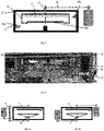
- FIG. 3 shows a first embodiment of the invention.
- the spin rinse dryer of Figure 3 includes an enclosure formed by a main body 21 and a lid 22, with a rotatable support 23 for the wafer 29.
- a rotatable member 27 Located above the wafer 29 and below the lid 22 of the enclosure is a rotatable member 27, in the form of a disc with a continuous lower surface. Any liquid that splashes up from the wafer 29 during cleaning will strike the lower surface of the rotatable member 27, rather than the lid 22 of the enclosure, so droplets will form on the rotatable member 27 instead of the lid 22.
- the rotatable member 27 can then be rotated to remove the droplets from the lower surface via centrifugal force.
- the rotatable support 23 for the wafer 29 and the rotatable member 27 are formed integrally.
- Three circumferentially equispaced arms extend downwards from the rotatable member 27, and the wafer 29 is supported on three prongs which extend radially inwardly from the lower ends of the arms.
- the rotatable member 27, and thus the arms and prongs, are rotated by a central shaft 25 which extends vertically through the lid 22 of the enclosure.
- the central shaft 25 is powered to rotate by means of a motor 28 located to one side of the chamber, with the shaft of the motor 28 extending vertically and being connected to the central shaft 25 by a belt drive 26. Arranging the drive means alongside the enclosure reduces the overall height of the spin rinse dryer.
- the rotatable member 27 and the rotatable support 23 for the wafer 29 are rotated (typically at 50 to 200 rpm) while cleaning fluid is sprayed from nozzles 24a and 24b. All of the internal surfaces of the chamber will be wetted with scattered spray, and this has the potential to form hanging liquid droplets (similar to those shown in Figure 1b ), which could fall on to the wafer 29.
- the fluid supply is turned off and the wafer 29 is dried by rotation at high speed (typically 2000 to 2500 rpm).
- An inert drying purge gas such as nitrogen can also be used.
- This high speed rotation not only is the wafer 29 dried (by centrifugal forces moving water radially away from the wafer 29), but so is the rotatable member 27 which is located directly above the wafer 29.
- the droplets formed on the rotatable member 27 will be thrown off by centrifugal force.
- the rotatable member 27 has a larger diameter than the wafer 29; for example, if the wafer 29 has a diameter of 300mm, the rotatable member 27 would have a diameter of 320mm. Further, the rotatable member 27 should extend as close as possible to the chamber walls, and preferably to within at most 10mm of the chamber walls. This further reduces the risk of liquid dripping from the lower surface of the lid 22 of the chamber onto the wafer 29. Drainage channels for fluid can be located near the chamber walls.
- the top of the rotatable member 27 should be positioned close to the lower surface of the lid 22 of the chamber (to reduce the risk of spray from the nozzles hitting the lower surface of the lid 22 of the chamber), and is preferably positioned within 3mm of the lower surface of the lid 22 of the chamber.
- Figure 4 shows a low profile spin rinse dryer with the chamber open to allowing loading or unloading of a wafer.
- the lower part 31 of the chamber moves away from the upper part 32, which is fixed, but it would also be possible for the lower part 31 of the chamber to be fixed and for the upper part of the chamber to be moved 32.
- This opening and closing movement can be achieved using electric motors or pneumatic or hydraulic pistons.
- the wafer 39 When the chamber is open, the wafer 39 can be inserted into or removed from the rotatable support 33.
- the inner diameter between the holding arms must be greater than the diameter of the wafer 39 to allow the wafer 39 to be placed into the chamber and onto the rotatable support 33.
- notch alignment is required, then the position of the wafer 39 in the rotatable support 33 needs to be rotationally aligned before wafer loading or unloading can occur. This is achieved by a central lift pillar 40 which lifts the wafer 39 from the rotatable support 33 and enables the alignment of a notch or flat on the wafer 39 to a defined orientation on the rotatable support prior to the unloading step.
- the particular version of the chamber in Figure 4 has a maximum height when opened of around 215mm; this allows the chambers to be stacked with a pitch of around 225mm, leading to an efficient use of space.
- Figure 5a shows a variant in which the rotatable support 53 and the rotatable member 54 are separate bodies arranged to rotate about a common axis.
- the rotatable support 53 for the wafer supports the wafer from below, which may simplify the procedure of loading and unloading the wafer.
- the rotatable support 53 and rotatable member 54 are driven by a single motor 51, and are connected thereto via a telescopic shaft coupling 52 (the telescopic aspect is necessary to allow the upper and lower parts of the chamber to move away from each other to open the chamber).
- Figure 5b shows an alternative version in which separate motors 61, 62 are provided for the rotatable support 63 and the rotatable member 64, which again are arranged to rotate about a common axis.
- the motor or motors 61, 62 are arranged to the side of the chamber, to keep the overall height as low as possible.
- the rotatable support and the rotatable member are two distinct entities, it is possible to reduce the overall size of the rotor assembly, which in turn can result in a chamber with a smaller diameter.
- the arrangements shown in Figures 5a and 5b can also allow more process flexibility for cleaning and drying the wafer, as they both allow the rotatable support and the rotatable member to be rotated at different speeds. Further, the arrangement shown in Figure 5b allows the rotatable support and the rotatable member to be spun independently of each other.
- the rotatable member When operating with two drive assemblies, the rotatable member will typically have a maximum speed less than that of the wafer (less than or equal to around 1000rpm), as it contains no surface morphology which needs to be dried, and only requires the removal of larger droplets of liquid. If the process uses a deionized water clean, then the rotatable member can be made from a hydrophobic plastic material, such as polycarbonate, although the choice of material will of course be dependent on compatibility with the process chemistry.
- the rotatable member will typically be machined or moulded as a single part, to ensure mechanical robustness. Further, the rotatable member may be formed with ribs or similar reinforcing features radiating out from the centre to increase its rigidity.
- FIGS 3, 5a and 5b only show a limited number of wetting nozzles.
- a spin rinse dryer will feature several wetting nozzles able to access both the upper and lower surfaces (front and back) of the wafer.
- Different flow rates, drive pressures and spray shapes of the nozzles can be used, depending on the process requirements.
- Common options for spray shape are fans and solid cones. Typical nozzle flow rates are 1 litre per minute at 35 psi (around 240 kPa), and so a spin rinse dryer using four fluid nozzles would run at 4 litres per minute.
- the chamber may be sealed during water delivery, which can allow wafers to be processed at pressures below atmospheric, typically 10 to 100 Torr (around 133 to 1330 Pa).
Landscapes
- Engineering & Computer Science (AREA)
- Mechanical Engineering (AREA)
- General Engineering & Computer Science (AREA)
- Health & Medical Sciences (AREA)
- Life Sciences & Earth Sciences (AREA)
- Molecular Biology (AREA)
- Cleaning Or Drying Semiconductors (AREA)
- Container, Conveyance, Adherence, Positioning, Of Wafer (AREA)
Applications Claiming Priority (1)
| Application Number | Priority Date | Filing Date | Title |
|---|---|---|---|
| GBGB2018030.3A GB202018030D0 (en) | 2020-11-17 | 2020-11-17 | Spin rinse dryer with improved drying characteristics |
Publications (2)
| Publication Number | Publication Date |
|---|---|
| EP4002433A1 true EP4002433A1 (de) | 2022-05-25 |
| EP4002433B1 EP4002433B1 (de) | 2023-05-10 |
Family
ID=74046652
Family Applications (1)
| Application Number | Title | Priority Date | Filing Date |
|---|---|---|---|
| EP21194938.3A Active EP4002433B1 (de) | 2020-11-17 | 2021-09-03 | Schleuder-, spül- und trocknermodul mit verbesserten trocknungseigenschaften |
Country Status (6)
| Country | Link |
|---|---|
| US (1) | US12590760B2 (de) |
| EP (1) | EP4002433B1 (de) |
| JP (1) | JP7734043B2 (de) |
| KR (1) | KR102895598B1 (de) |
| CN (1) | CN114512420A (de) |
| GB (1) | GB202018030D0 (de) |
Families Citing this family (1)
| Publication number | Priority date | Publication date | Assignee | Title |
|---|---|---|---|---|
| CN117308536B (zh) * | 2023-12-01 | 2024-02-09 | 山东雍联新材料科技有限公司 | 一种钙基膨润土钠化干燥回转炉 |
Citations (6)
| Publication number | Priority date | Publication date | Assignee | Title |
|---|---|---|---|---|
| US6497241B1 (en) | 1999-12-23 | 2002-12-24 | Lam Research Corporation | Hollow core spindle and spin, rinse, and dry module including the same |
| EP1848025A1 (de) * | 2006-04-18 | 2007-10-24 | Tokyo Electron Limited | Flüssigkeitsverarbeitungsvorrichtung |
| US20130125931A1 (en) * | 2011-11-21 | 2013-05-23 | Tokyo Electron Limited | Liquid processing apparatus and liquid processing method |
| US20150090694A1 (en) * | 2012-03-30 | 2015-04-02 | Koji Hashimoto | Substrate processing device and substrate processing method |
| US9421617B2 (en) | 2011-06-22 | 2016-08-23 | Tel Nexx, Inc. | Substrate holder |
| US20170186599A1 (en) * | 2015-12-24 | 2017-06-29 | SCREEN Holdings Co., Ltd. | Substrate processing apparatus and substrate processing method |
Family Cites Families (23)
| Publication number | Priority date | Publication date | Assignee | Title |
|---|---|---|---|---|
| US5232511A (en) * | 1990-05-15 | 1993-08-03 | Semitool, Inc. | Dynamic semiconductor wafer processing using homogeneous mixed acid vapors |
| JP3321725B2 (ja) * | 1995-05-12 | 2002-09-09 | 東京エレクトロン株式会社 | 洗浄装置 |
| JP3831043B2 (ja) | 1997-01-24 | 2006-10-11 | 東京エレクトロン株式会社 | 回転処理装置 |
| JP3555724B2 (ja) * | 1997-09-04 | 2004-08-18 | 大日本スクリーン製造株式会社 | 基板処理装置 |
| JP2000049215A (ja) | 1998-07-28 | 2000-02-18 | Tokyo Electron Ltd | 処理システム |
| KR100360402B1 (ko) * | 2000-03-22 | 2002-11-13 | 삼성전자 주식회사 | 회전성 분사노즐을 구비하는 웨이퍼 건조 장치 및 이를이용한 웨이퍼 건조 방법 |
| JP2003151941A (ja) | 2001-11-16 | 2003-05-23 | Dainippon Screen Mfg Co Ltd | 基板処理装置 |
| US6742279B2 (en) * | 2002-01-16 | 2004-06-01 | Applied Materials Inc. | Apparatus and method for rinsing substrates |
| US7584760B2 (en) * | 2002-09-13 | 2009-09-08 | Dainippon Screen Mfg. Co., Ltd. | Substrate processing apparatus |
| JP4933945B2 (ja) | 2006-04-18 | 2012-05-16 | 東京エレクトロン株式会社 | 液処理装置 |
| JP5159587B2 (ja) | 2008-12-05 | 2013-03-06 | 黒田精工株式会社 | 表面形状測定装置 |
| US8172646B2 (en) | 2009-02-27 | 2012-05-08 | Novellus Systems, Inc. | Magnetically actuated chuck for edge bevel removal |
| US9455139B2 (en) | 2009-06-17 | 2016-09-27 | Novellus Systems, Inc. | Methods and apparatus for wetting pretreatment for through resist metal plating |
| US9589817B2 (en) * | 2011-04-15 | 2017-03-07 | Illinois Tool Works Inc. | Dryer |
| JP5844104B2 (ja) | 2011-09-28 | 2016-01-13 | 株式会社Screenホールディングス | スリットノズルおよび基板処理装置 |
| JP5926086B2 (ja) | 2012-03-28 | 2016-05-25 | 株式会社Screenホールディングス | 基板処理装置および基板処理方法 |
| JP2014011370A (ja) | 2012-07-02 | 2014-01-20 | Disco Abrasive Syst Ltd | 加工装置 |
| JP6279276B2 (ja) | 2013-10-03 | 2018-02-14 | 株式会社荏原製作所 | 基板洗浄装置及び基板処理装置 |
| JP6523082B2 (ja) | 2015-07-13 | 2019-05-29 | 帝人株式会社 | ポリカーボネート樹脂 |
| TWI706433B (zh) | 2016-07-12 | 2020-10-01 | 大陸商盛美半導體設備(上海)股份有限公司 | 用於清洗和乾燥積體電路基板的方法和裝置 |
| GB201701166D0 (en) | 2017-01-24 | 2017-03-08 | Picofluidics Ltd | An apparatus for electrochemically processing semiconductor substrates |
| JP7045867B2 (ja) | 2018-01-26 | 2022-04-01 | 株式会社Screenホールディングス | 基板処理方法 |
| KR102775038B1 (ko) * | 2019-03-28 | 2025-03-05 | 삼성디스플레이 주식회사 | 감압 건조 장치 |
-
2020
- 2020-11-17 GB GBGB2018030.3A patent/GB202018030D0/en not_active Ceased
-
2021
- 2021-09-03 EP EP21194938.3A patent/EP4002433B1/de active Active
- 2021-09-16 CN CN202111085987.8A patent/CN114512420A/zh active Pending
- 2021-10-22 KR KR1020210141830A patent/KR102895598B1/ko active Active
- 2021-10-22 JP JP2021173208A patent/JP7734043B2/ja active Active
- 2021-10-25 US US17/510,333 patent/US12590760B2/en active Active
Patent Citations (6)
| Publication number | Priority date | Publication date | Assignee | Title |
|---|---|---|---|---|
| US6497241B1 (en) | 1999-12-23 | 2002-12-24 | Lam Research Corporation | Hollow core spindle and spin, rinse, and dry module including the same |
| EP1848025A1 (de) * | 2006-04-18 | 2007-10-24 | Tokyo Electron Limited | Flüssigkeitsverarbeitungsvorrichtung |
| US9421617B2 (en) | 2011-06-22 | 2016-08-23 | Tel Nexx, Inc. | Substrate holder |
| US20130125931A1 (en) * | 2011-11-21 | 2013-05-23 | Tokyo Electron Limited | Liquid processing apparatus and liquid processing method |
| US20150090694A1 (en) * | 2012-03-30 | 2015-04-02 | Koji Hashimoto | Substrate processing device and substrate processing method |
| US20170186599A1 (en) * | 2015-12-24 | 2017-06-29 | SCREEN Holdings Co., Ltd. | Substrate processing apparatus and substrate processing method |
Also Published As
| Publication number | Publication date |
|---|---|
| US12590760B2 (en) | 2026-03-31 |
| EP4002433B1 (de) | 2023-05-10 |
| TW202226415A (zh) | 2022-07-01 |
| CN114512420A (zh) | 2022-05-17 |
| US20220155011A1 (en) | 2022-05-19 |
| JP7734043B2 (ja) | 2025-09-04 |
| JP2022080274A (ja) | 2022-05-27 |
| KR102895598B1 (ko) | 2025-12-03 |
| GB202018030D0 (en) | 2020-12-30 |
| KR20220067489A (ko) | 2022-05-24 |
Similar Documents
| Publication | Publication Date | Title |
|---|---|---|
| CN100342487C (zh) | 处理微电子工件的微环境反应器 | |
| US6423642B1 (en) | Reactor for processing a semiconductor wafer | |
| CN102893372B (zh) | 具有流体分离特性的封闭室 | |
| US6548411B2 (en) | Apparatus and methods for processing a workpiece | |
| KR102758448B1 (ko) | 기판 처리 방법 및 기판 처리 장치 | |
| KR20100046800A (ko) | 매엽식 기판 처리 장치 및 그 장치에서의 배기 방법 | |
| CN106816399B (zh) | 基板处理装置及方法 | |
| KR20090070663A (ko) | 기판 처리 장치 | |
| JP2010226043A (ja) | 基板処理装置 | |
| US12590760B2 (en) | Spin rinse dryer with improved drying characteristics | |
| CN107591315B (zh) | 用于处理基板的装置和方法 | |
| US7938942B2 (en) | Single side workpiece processing | |
| JP2021034731A (ja) | 基板処理装置及び基板処理方法 | |
| KR102454444B1 (ko) | 기판 처리 장치 | |
| KR20240033289A (ko) | 기판들을 위한 습식 세정 스프레이 프로세스 챔버 | |
| TWI916435B (zh) | 具有改良乾燥特徵之旋轉清洗乾燥機 | |
| US8082932B2 (en) | Single side workpiece processing | |
| KR100915435B1 (ko) | 기판 처리 장치 및 기판 처리 방법 | |
| TWI861585B (zh) | 具備浸泡與清洗蝕刻功能的單晶圓旋轉清洗設備 | |
| JP7777463B2 (ja) | 基板処理装置、および処理カップの洗浄方法 | |
| KR20120077516A (ko) | 기판 처리 장치 | |
| KR101485579B1 (ko) | 기판세정장치 | |
| US20240116085A1 (en) | Substrate processing apparatus | |
| US20250166987A1 (en) | Apparatus and method of treating substrate | |
| TW202603969A (zh) | 基板保持裝置及濕法設備 |
Legal Events
| Date | Code | Title | Description |
|---|---|---|---|
| PUAI | Public reference made under article 153(3) epc to a published international application that has entered the european phase |
Free format text: ORIGINAL CODE: 0009012 |
|
| STAA | Information on the status of an ep patent application or granted ep patent |
Free format text: STATUS: THE APPLICATION HAS BEEN PUBLISHED |
|
| AK | Designated contracting states |
Kind code of ref document: A1 Designated state(s): AL AT BE BG CH CY CZ DE DK EE ES FI FR GB GR HR HU IE IS IT LI LT LU LV MC MK MT NL NO PL PT RO RS SE SI SK SM TR |
|
| STAA | Information on the status of an ep patent application or granted ep patent |
Free format text: STATUS: REQUEST FOR EXAMINATION WAS MADE |
|
| 17P | Request for examination filed |
Effective date: 20220805 |
|
| RBV | Designated contracting states (corrected) |
Designated state(s): AL AT BE BG CH CY CZ DE DK EE ES FI FR GB GR HR HU IE IS IT LI LT LU LV MC MK MT NL NO PL PT RO RS SE SI SK SM TR |
|
| GRAP | Despatch of communication of intention to grant a patent |
Free format text: ORIGINAL CODE: EPIDOSNIGR1 |
|
| STAA | Information on the status of an ep patent application or granted ep patent |
Free format text: STATUS: GRANT OF PATENT IS INTENDED |
|
| INTG | Intention to grant announced |
Effective date: 20230215 |
|
| GRAS | Grant fee paid |
Free format text: ORIGINAL CODE: EPIDOSNIGR3 |
|
| GRAA | (expected) grant |
Free format text: ORIGINAL CODE: 0009210 |
|
| STAA | Information on the status of an ep patent application or granted ep patent |
Free format text: STATUS: THE PATENT HAS BEEN GRANTED |
|
| AK | Designated contracting states |
Kind code of ref document: B1 Designated state(s): AL AT BE BG CH CY CZ DE DK EE ES FI FR GB GR HR HU IE IS IT LI LT LU LV MC MK MT NL NO PL PT RO RS SE SI SK SM TR |
|
| REG | Reference to a national code |
Ref country code: GB Ref legal event code: FG4D |
|
| REG | Reference to a national code |
Ref country code: AT Ref legal event code: REF Ref document number: 1567563 Country of ref document: AT Kind code of ref document: T Effective date: 20230515 Ref country code: CH Ref legal event code: EP |
|
| REG | Reference to a national code |
Ref country code: DE Ref legal event code: R096 Ref document number: 602021002303 Country of ref document: DE |
|
| REG | Reference to a national code |
Ref country code: IE Ref legal event code: FG4D |
|
| P01 | Opt-out of the competence of the unified patent court (upc) registered |
Effective date: 20230527 |
|
| REG | Reference to a national code |
Ref country code: LT Ref legal event code: MG9D |
|
| REG | Reference to a national code |
Ref country code: NL Ref legal event code: MP Effective date: 20230510 |
|
| REG | Reference to a national code |
Ref country code: AT Ref legal event code: MK05 Ref document number: 1567563 Country of ref document: AT Kind code of ref document: T Effective date: 20230510 |
|
| PG25 | Lapsed in a contracting state [announced via postgrant information from national office to epo] |
Ref country code: SE Free format text: LAPSE BECAUSE OF FAILURE TO SUBMIT A TRANSLATION OF THE DESCRIPTION OR TO PAY THE FEE WITHIN THE PRESCRIBED TIME-LIMIT Effective date: 20230510 Ref country code: PT Free format text: LAPSE BECAUSE OF FAILURE TO SUBMIT A TRANSLATION OF THE DESCRIPTION OR TO PAY THE FEE WITHIN THE PRESCRIBED TIME-LIMIT Effective date: 20230911 Ref country code: NO Free format text: LAPSE BECAUSE OF FAILURE TO SUBMIT A TRANSLATION OF THE DESCRIPTION OR TO PAY THE FEE WITHIN THE PRESCRIBED TIME-LIMIT Effective date: 20230810 Ref country code: NL Free format text: LAPSE BECAUSE OF FAILURE TO SUBMIT A TRANSLATION OF THE DESCRIPTION OR TO PAY THE FEE WITHIN THE PRESCRIBED TIME-LIMIT Effective date: 20230510 Ref country code: ES Free format text: LAPSE BECAUSE OF FAILURE TO SUBMIT A TRANSLATION OF THE DESCRIPTION OR TO PAY THE FEE WITHIN THE PRESCRIBED TIME-LIMIT Effective date: 20230510 Ref country code: AT Free format text: LAPSE BECAUSE OF FAILURE TO SUBMIT A TRANSLATION OF THE DESCRIPTION OR TO PAY THE FEE WITHIN THE PRESCRIBED TIME-LIMIT Effective date: 20230510 |
|
| REG | Reference to a national code |
Ref country code: DE Ref legal event code: R082 Ref document number: 602021002303 Country of ref document: DE Representative=s name: KANDLBINDER, MARKUS, DIPL.-PHYS., DE |
|
| PG25 | Lapsed in a contracting state [announced via postgrant information from national office to epo] |
Ref country code: RS Free format text: LAPSE BECAUSE OF FAILURE TO SUBMIT A TRANSLATION OF THE DESCRIPTION OR TO PAY THE FEE WITHIN THE PRESCRIBED TIME-LIMIT Effective date: 20230510 Ref country code: PL Free format text: LAPSE BECAUSE OF FAILURE TO SUBMIT A TRANSLATION OF THE DESCRIPTION OR TO PAY THE FEE WITHIN THE PRESCRIBED TIME-LIMIT Effective date: 20230510 Ref country code: LV Free format text: LAPSE BECAUSE OF FAILURE TO SUBMIT A TRANSLATION OF THE DESCRIPTION OR TO PAY THE FEE WITHIN THE PRESCRIBED TIME-LIMIT Effective date: 20230510 Ref country code: LT Free format text: LAPSE BECAUSE OF FAILURE TO SUBMIT A TRANSLATION OF THE DESCRIPTION OR TO PAY THE FEE WITHIN THE PRESCRIBED TIME-LIMIT Effective date: 20230510 Ref country code: IS Free format text: LAPSE BECAUSE OF FAILURE TO SUBMIT A TRANSLATION OF THE DESCRIPTION OR TO PAY THE FEE WITHIN THE PRESCRIBED TIME-LIMIT Effective date: 20230910 Ref country code: HR Free format text: LAPSE BECAUSE OF FAILURE TO SUBMIT A TRANSLATION OF THE DESCRIPTION OR TO PAY THE FEE WITHIN THE PRESCRIBED TIME-LIMIT Effective date: 20230510 Ref country code: GR Free format text: LAPSE BECAUSE OF FAILURE TO SUBMIT A TRANSLATION OF THE DESCRIPTION OR TO PAY THE FEE WITHIN THE PRESCRIBED TIME-LIMIT Effective date: 20230811 |
|
| PG25 | Lapsed in a contracting state [announced via postgrant information from national office to epo] |
Ref country code: FI Free format text: LAPSE BECAUSE OF FAILURE TO SUBMIT A TRANSLATION OF THE DESCRIPTION OR TO PAY THE FEE WITHIN THE PRESCRIBED TIME-LIMIT Effective date: 20230510 |
|
| PG25 | Lapsed in a contracting state [announced via postgrant information from national office to epo] |
Ref country code: SK Free format text: LAPSE BECAUSE OF FAILURE TO SUBMIT A TRANSLATION OF THE DESCRIPTION OR TO PAY THE FEE WITHIN THE PRESCRIBED TIME-LIMIT Effective date: 20230510 |
|
| PG25 | Lapsed in a contracting state [announced via postgrant information from national office to epo] |
Ref country code: SM Free format text: LAPSE BECAUSE OF FAILURE TO SUBMIT A TRANSLATION OF THE DESCRIPTION OR TO PAY THE FEE WITHIN THE PRESCRIBED TIME-LIMIT Effective date: 20230510 Ref country code: SK Free format text: LAPSE BECAUSE OF FAILURE TO SUBMIT A TRANSLATION OF THE DESCRIPTION OR TO PAY THE FEE WITHIN THE PRESCRIBED TIME-LIMIT Effective date: 20230510 Ref country code: RO Free format text: LAPSE BECAUSE OF FAILURE TO SUBMIT A TRANSLATION OF THE DESCRIPTION OR TO PAY THE FEE WITHIN THE PRESCRIBED TIME-LIMIT Effective date: 20230510 Ref country code: EE Free format text: LAPSE BECAUSE OF FAILURE TO SUBMIT A TRANSLATION OF THE DESCRIPTION OR TO PAY THE FEE WITHIN THE PRESCRIBED TIME-LIMIT Effective date: 20230510 Ref country code: DK Free format text: LAPSE BECAUSE OF FAILURE TO SUBMIT A TRANSLATION OF THE DESCRIPTION OR TO PAY THE FEE WITHIN THE PRESCRIBED TIME-LIMIT Effective date: 20230510 Ref country code: CZ Free format text: LAPSE BECAUSE OF FAILURE TO SUBMIT A TRANSLATION OF THE DESCRIPTION OR TO PAY THE FEE WITHIN THE PRESCRIBED TIME-LIMIT Effective date: 20230510 |
|
| REG | Reference to a national code |
Ref country code: DE Ref legal event code: R097 Ref document number: 602021002303 Country of ref document: DE |
|
| PLBE | No opposition filed within time limit |
Free format text: ORIGINAL CODE: 0009261 |
|
| STAA | Information on the status of an ep patent application or granted ep patent |
Free format text: STATUS: NO OPPOSITION FILED WITHIN TIME LIMIT |
|
| 26N | No opposition filed |
Effective date: 20240213 |
|
| PG25 | Lapsed in a contracting state [announced via postgrant information from national office to epo] |
Ref country code: SI Free format text: LAPSE BECAUSE OF FAILURE TO SUBMIT A TRANSLATION OF THE DESCRIPTION OR TO PAY THE FEE WITHIN THE PRESCRIBED TIME-LIMIT Effective date: 20230510 |
|
| PG25 | Lapsed in a contracting state [announced via postgrant information from national office to epo] |
Ref country code: LU Free format text: LAPSE BECAUSE OF NON-PAYMENT OF DUE FEES Effective date: 20230903 |
|
| REG | Reference to a national code |
Ref country code: BE Ref legal event code: MM Effective date: 20230930 |
|
| PG25 | Lapsed in a contracting state [announced via postgrant information from national office to epo] |
Ref country code: SI Free format text: LAPSE BECAUSE OF FAILURE TO SUBMIT A TRANSLATION OF THE DESCRIPTION OR TO PAY THE FEE WITHIN THE PRESCRIBED TIME-LIMIT Effective date: 20230510 Ref country code: LU Free format text: LAPSE BECAUSE OF NON-PAYMENT OF DUE FEES Effective date: 20230903 Ref country code: IT Free format text: LAPSE BECAUSE OF FAILURE TO SUBMIT A TRANSLATION OF THE DESCRIPTION OR TO PAY THE FEE WITHIN THE PRESCRIBED TIME-LIMIT Effective date: 20230510 Ref country code: MC Free format text: LAPSE BECAUSE OF FAILURE TO SUBMIT A TRANSLATION OF THE DESCRIPTION OR TO PAY THE FEE WITHIN THE PRESCRIBED TIME-LIMIT Effective date: 20230510 |
|
| REG | Reference to a national code |
Ref country code: IE Ref legal event code: MM4A |
|
| PG25 | Lapsed in a contracting state [announced via postgrant information from national office to epo] |
Ref country code: IE Free format text: LAPSE BECAUSE OF NON-PAYMENT OF DUE FEES Effective date: 20230903 |
|
| PG25 | Lapsed in a contracting state [announced via postgrant information from national office to epo] |
Ref country code: IE Free format text: LAPSE BECAUSE OF NON-PAYMENT OF DUE FEES Effective date: 20230903 |
|
| PG25 | Lapsed in a contracting state [announced via postgrant information from national office to epo] |
Ref country code: BE Free format text: LAPSE BECAUSE OF NON-PAYMENT OF DUE FEES Effective date: 20230930 |
|
| PG25 | Lapsed in a contracting state [announced via postgrant information from national office to epo] |
Ref country code: BG Free format text: LAPSE BECAUSE OF FAILURE TO SUBMIT A TRANSLATION OF THE DESCRIPTION OR TO PAY THE FEE WITHIN THE PRESCRIBED TIME-LIMIT Effective date: 20230510 |
|
| PG25 | Lapsed in a contracting state [announced via postgrant information from national office to epo] |
Ref country code: BG Free format text: LAPSE BECAUSE OF FAILURE TO SUBMIT A TRANSLATION OF THE DESCRIPTION OR TO PAY THE FEE WITHIN THE PRESCRIBED TIME-LIMIT Effective date: 20230510 |
|
| REG | Reference to a national code |
Ref country code: CH Ref legal event code: PL |
|
| PG25 | Lapsed in a contracting state [announced via postgrant information from national office to epo] |
Ref country code: CH Free format text: LAPSE BECAUSE OF NON-PAYMENT OF DUE FEES Effective date: 20240930 |
|
| PG25 | Lapsed in a contracting state [announced via postgrant information from national office to epo] |
Ref country code: CY Free format text: LAPSE BECAUSE OF FAILURE TO SUBMIT A TRANSLATION OF THE DESCRIPTION OR TO PAY THE FEE WITHIN THE PRESCRIBED TIME-LIMIT; INVALID AB INITIO Effective date: 20210903 |
|
| PG25 | Lapsed in a contracting state [announced via postgrant information from national office to epo] |
Ref country code: HU Free format text: LAPSE BECAUSE OF FAILURE TO SUBMIT A TRANSLATION OF THE DESCRIPTION OR TO PAY THE FEE WITHIN THE PRESCRIBED TIME-LIMIT; INVALID AB INITIO Effective date: 20210903 |
|
| PGFP | Annual fee paid to national office [announced via postgrant information from national office to epo] |
Ref country code: DE Payment date: 20250929 Year of fee payment: 5 |
|
| PGFP | Annual fee paid to national office [announced via postgrant information from national office to epo] |
Ref country code: FR Payment date: 20250925 Year of fee payment: 5 |
|
| REG | Reference to a national code |
Ref country code: DE Ref legal event code: R079 Ref document number: 602021002303 Country of ref document: DE Free format text: PREVIOUS MAIN CLASS: H01L0021670000 Ipc: H10P0072000000 |
|
| PG25 | Lapsed in a contracting state [announced via postgrant information from national office to epo] |
Ref country code: TR Free format text: LAPSE BECAUSE OF FAILURE TO SUBMIT A TRANSLATION OF THE DESCRIPTION OR TO PAY THE FEE WITHIN THE PRESCRIBED TIME-LIMIT Effective date: 20230510 |