EP4002435A1 - Dispositif semi-conducteur avec réseau de distribution de puissance arrière et son procédé de fabrication - Google Patents
Dispositif semi-conducteur avec réseau de distribution de puissance arrière et son procédé de fabrication Download PDFInfo
- Publication number
- EP4002435A1 EP4002435A1 EP21176650.6A EP21176650A EP4002435A1 EP 4002435 A1 EP4002435 A1 EP 4002435A1 EP 21176650 A EP21176650 A EP 21176650A EP 4002435 A1 EP4002435 A1 EP 4002435A1
- Authority
- EP
- European Patent Office
- Prior art keywords
- landing pad
- wafer
- semiconductor device
- tsv
- semiconductor
- Prior art date
- Legal status (The legal status is an assumption and is not a legal conclusion. Google has not performed a legal analysis and makes no representation as to the accuracy of the status listed.)
- Granted
Links
Images









Classifications
-
- H—ELECTRICITY
- H10—SEMICONDUCTOR DEVICES; ELECTRIC SOLID-STATE DEVICES NOT OTHERWISE PROVIDED FOR
- H10D—INORGANIC ELECTRIC SEMICONDUCTOR DEVICES
- H10D84/00—Integrated devices formed in or on semiconductor substrates that comprise only semiconducting layers, e.g. on Si wafers or on GaAs-on-Si wafers
- H10D84/01—Manufacture or treatment
- H10D84/02—Manufacture or treatment characterised by using material-based technologies
- H10D84/03—Manufacture or treatment characterised by using material-based technologies using Group IV technology, e.g. silicon technology or silicon-carbide [SiC] technology
- H10D84/038—Manufacture or treatment characterised by using material-based technologies using Group IV technology, e.g. silicon technology or silicon-carbide [SiC] technology using silicon technology, e.g. SiGe
-
- H—ELECTRICITY
- H10—SEMICONDUCTOR DEVICES; ELECTRIC SOLID-STATE DEVICES NOT OTHERWISE PROVIDED FOR
- H10D—INORGANIC ELECTRIC SEMICONDUCTOR DEVICES
- H10D88/00—Three-dimensional [3D] integrated devices
-
- H—ELECTRICITY
- H10—SEMICONDUCTOR DEVICES; ELECTRIC SOLID-STATE DEVICES NOT OTHERWISE PROVIDED FOR
- H10D—INORGANIC ELECTRIC SEMICONDUCTOR DEVICES
- H10D88/00—Three-dimensional [3D] integrated devices
- H10D88/01—Manufacture or treatment
-
- H—ELECTRICITY
- H10—SEMICONDUCTOR DEVICES; ELECTRIC SOLID-STATE DEVICES NOT OTHERWISE PROVIDED FOR
- H10D—INORGANIC ELECTRIC SEMICONDUCTOR DEVICES
- H10D88/00—Three-dimensional [3D] integrated devices
- H10D88/101—Three-dimensional [3D] integrated devices comprising components on opposite major surfaces of semiconductor substrates
-
- H—ELECTRICITY
- H10—SEMICONDUCTOR DEVICES; ELECTRIC SOLID-STATE DEVICES NOT OTHERWISE PROVIDED FOR
- H10W—GENERIC PACKAGES, INTERCONNECTIONS, CONNECTORS OR OTHER CONSTRUCTIONAL DETAILS OF DEVICES COVERED BY CLASS H10
- H10W20/00—Interconnections in chips, wafers or substrates
- H10W20/01—Manufacture or treatment
- H10W20/021—Manufacture or treatment of interconnections within wafers or substrates
-
- H—ELECTRICITY
- H10—SEMICONDUCTOR DEVICES; ELECTRIC SOLID-STATE DEVICES NOT OTHERWISE PROVIDED FOR
- H10W—GENERIC PACKAGES, INTERCONNECTIONS, CONNECTORS OR OTHER CONSTRUCTIONAL DETAILS OF DEVICES COVERED BY CLASS H10
- H10W20/00—Interconnections in chips, wafers or substrates
- H10W20/01—Manufacture or treatment
- H10W20/021—Manufacture or treatment of interconnections within wafers or substrates
- H10W20/023—Manufacture or treatment of interconnections within wafers or substrates the interconnections being through-semiconductor vias
-
- H—ELECTRICITY
- H10—SEMICONDUCTOR DEVICES; ELECTRIC SOLID-STATE DEVICES NOT OTHERWISE PROVIDED FOR
- H10W—GENERIC PACKAGES, INTERCONNECTIONS, CONNECTORS OR OTHER CONSTRUCTIONAL DETAILS OF DEVICES COVERED BY CLASS H10
- H10W20/00—Interconnections in chips, wafers or substrates
- H10W20/01—Manufacture or treatment
- H10W20/021—Manufacture or treatment of interconnections within wafers or substrates
- H10W20/023—Manufacture or treatment of interconnections within wafers or substrates the interconnections being through-semiconductor vias
- H10W20/0234—Manufacture or treatment of interconnections within wafers or substrates the interconnections being through-semiconductor vias comprising etching via holes that stop on pads or on electrodes
-
- H—ELECTRICITY
- H10—SEMICONDUCTOR DEVICES; ELECTRIC SOLID-STATE DEVICES NOT OTHERWISE PROVIDED FOR
- H10W—GENERIC PACKAGES, INTERCONNECTIONS, CONNECTORS OR OTHER CONSTRUCTIONAL DETAILS OF DEVICES COVERED BY CLASS H10
- H10W20/00—Interconnections in chips, wafers or substrates
- H10W20/01—Manufacture or treatment
- H10W20/021—Manufacture or treatment of interconnections within wafers or substrates
- H10W20/023—Manufacture or treatment of interconnections within wafers or substrates the interconnections being through-semiconductor vias
- H10W20/0242—Manufacture or treatment of interconnections within wafers or substrates the interconnections being through-semiconductor vias comprising etching via holes from the back sides of the chips, wafers or substrates
-
- H—ELECTRICITY
- H10—SEMICONDUCTOR DEVICES; ELECTRIC SOLID-STATE DEVICES NOT OTHERWISE PROVIDED FOR
- H10W—GENERIC PACKAGES, INTERCONNECTIONS, CONNECTORS OR OTHER CONSTRUCTIONAL DETAILS OF DEVICES COVERED BY CLASS H10
- H10W20/00—Interconnections in chips, wafers or substrates
- H10W20/01—Manufacture or treatment
- H10W20/031—Manufacture or treatment of conductive parts of the interconnections
-
- H—ELECTRICITY
- H10—SEMICONDUCTOR DEVICES; ELECTRIC SOLID-STATE DEVICES NOT OTHERWISE PROVIDED FOR
- H10W—GENERIC PACKAGES, INTERCONNECTIONS, CONNECTORS OR OTHER CONSTRUCTIONAL DETAILS OF DEVICES COVERED BY CLASS H10
- H10W20/00—Interconnections in chips, wafers or substrates
- H10W20/20—Interconnections within wafers or substrates, e.g. through-silicon vias [TSV]
-
- H—ELECTRICITY
- H10—SEMICONDUCTOR DEVICES; ELECTRIC SOLID-STATE DEVICES NOT OTHERWISE PROVIDED FOR
- H10W—GENERIC PACKAGES, INTERCONNECTIONS, CONNECTORS OR OTHER CONSTRUCTIONAL DETAILS OF DEVICES COVERED BY CLASS H10
- H10W20/00—Interconnections in chips, wafers or substrates
- H10W20/20—Interconnections within wafers or substrates, e.g. through-silicon vias [TSV]
- H10W20/211—Through-semiconductor vias, e.g. TSVs
- H10W20/218—Through-semiconductor vias, e.g. TSVs in silicon-on-insulator [SOI] wafers
-
- H—ELECTRICITY
- H10—SEMICONDUCTOR DEVICES; ELECTRIC SOLID-STATE DEVICES NOT OTHERWISE PROVIDED FOR
- H10W—GENERIC PACKAGES, INTERCONNECTIONS, CONNECTORS OR OTHER CONSTRUCTIONAL DETAILS OF DEVICES COVERED BY CLASS H10
- H10W20/00—Interconnections in chips, wafers or substrates
- H10W20/40—Interconnections external to wafers or substrates, e.g. back-end-of-line [BEOL] metallisations or vias connecting to gate electrodes
- H10W20/41—Interconnections external to wafers or substrates, e.g. back-end-of-line [BEOL] metallisations or vias connecting to gate electrodes characterised by their conductive parts
- H10W20/427—Power or ground buses
-
- H—ELECTRICITY
- H10—SEMICONDUCTOR DEVICES; ELECTRIC SOLID-STATE DEVICES NOT OTHERWISE PROVIDED FOR
- H10W—GENERIC PACKAGES, INTERCONNECTIONS, CONNECTORS OR OTHER CONSTRUCTIONAL DETAILS OF DEVICES COVERED BY CLASS H10
- H10W20/00—Interconnections in chips, wafers or substrates
- H10W20/40—Interconnections external to wafers or substrates, e.g. back-end-of-line [BEOL] metallisations or vias connecting to gate electrodes
- H10W20/41—Interconnections external to wafers or substrates, e.g. back-end-of-line [BEOL] metallisations or vias connecting to gate electrodes characterised by their conductive parts
- H10W20/435—Cross-sectional shapes or dispositions of interconnections
-
- H—ELECTRICITY
- H10—SEMICONDUCTOR DEVICES; ELECTRIC SOLID-STATE DEVICES NOT OTHERWISE PROVIDED FOR
- H10W—GENERIC PACKAGES, INTERCONNECTIONS, CONNECTORS OR OTHER CONSTRUCTIONAL DETAILS OF DEVICES COVERED BY CLASS H10
- H10W20/00—Interconnections in chips, wafers or substrates
- H10W20/40—Interconnections external to wafers or substrates, e.g. back-end-of-line [BEOL] metallisations or vias connecting to gate electrodes
- H10W20/481—Interconnections external to wafers or substrates, e.g. back-end-of-line [BEOL] metallisations or vias connecting to gate electrodes on the rear surfaces of the wafers or substrates
-
- H—ELECTRICITY
- H10—SEMICONDUCTOR DEVICES; ELECTRIC SOLID-STATE DEVICES NOT OTHERWISE PROVIDED FOR
- H10W—GENERIC PACKAGES, INTERCONNECTIONS, CONNECTORS OR OTHER CONSTRUCTIONAL DETAILS OF DEVICES COVERED BY CLASS H10
- H10W70/00—Package substrates; Interposers; Redistribution layers [RDL]
- H10W70/60—Insulating or insulated package substrates; Interposers; Redistribution layers
- H10W70/62—Insulating or insulated package substrates; Interposers; Redistribution layers characterised by their interconnections
- H10W70/65—Shapes or dispositions of interconnections
-
- H—ELECTRICITY
- H10—SEMICONDUCTOR DEVICES; ELECTRIC SOLID-STATE DEVICES NOT OTHERWISE PROVIDED FOR
- H10W—GENERIC PACKAGES, INTERCONNECTIONS, CONNECTORS OR OTHER CONSTRUCTIONAL DETAILS OF DEVICES COVERED BY CLASS H10
- H10W72/00—Interconnections or connectors in packages
- H10W72/90—Bond pads, in general
- H10W72/921—Structures or relative sizes of bond pads
- H10W72/923—Bond pads having multiple stacked layers
-
- H—ELECTRICITY
- H10—SEMICONDUCTOR DEVICES; ELECTRIC SOLID-STATE DEVICES NOT OTHERWISE PROVIDED FOR
- H10W—GENERIC PACKAGES, INTERCONNECTIONS, CONNECTORS OR OTHER CONSTRUCTIONAL DETAILS OF DEVICES COVERED BY CLASS H10
- H10W72/00—Interconnections or connectors in packages
- H10W72/90—Bond pads, in general
- H10W72/941—Dispositions of bond pads
- H10W72/942—Dispositions of bond pads relative to underlying supporting features, e.g. bond pads, RDLs or vias
-
- H—ELECTRICITY
- H10—SEMICONDUCTOR DEVICES; ELECTRIC SOLID-STATE DEVICES NOT OTHERWISE PROVIDED FOR
- H10W—GENERIC PACKAGES, INTERCONNECTIONS, CONNECTORS OR OTHER CONSTRUCTIONAL DETAILS OF DEVICES COVERED BY CLASS H10
- H10W72/00—Interconnections or connectors in packages
- H10W72/90—Bond pads, in general
- H10W72/951—Materials of bond pads
- H10W72/952—Materials of bond pads comprising metals or metalloids, e.g. PbSn, Ag or Cu
Definitions
- Example embodiments of the present disclosure relate to a backside power distribution network (BSPDN) semiconductor architecture and a method of manufacturing the same, and more particularly to a BSPDN semiconductor architecture including a landing pad and a method of manufacturing the same.
- BSPDN backside power distribution network
- the BSPDN semiconductor architecture separates the signal wiring from the power distribution network (PDN) in a semiconductor device by providing an integrated circuit including active transistors, signal wires, and buried power rails (BPRs) on a first side of a wafer and providing the PDN on a second side of the wafer.
- the BSPDN semiconductor architecture may minimize the routing congestion and allow for down scaling of an area of the semiconductor architecture.
- a BSPDN semiconductor architecture may result in a ⁇ 30 % reduction and an improved current-resistance (IR) drop as compared to a general PDN semiconductor architecture.
- BSPDN semiconductor architectures may be difficult. For example, a misalignment between a buried power rail (BPR) included in the integrated circuit integrated on the first side of the wafer with a through-silicon via (TSV) protruding from the PDN integrated on the second side of the wafer may occur. Such misalignment between the BPR and the TSV may lead to an increase in resistance and device failure of the semiconductor architecture.
- BPR buried power rail
- TSV through-silicon via
- One or more example embodiments provide a backside power distribution network (BSPDN) semiconductor architecture and a method of manufacturing the same.
- BSPDN backside power distribution network
- One or more example embodiments also provide to a BSPDN semiconductor architecture including a landing pad and a method of manufacturing the same.
- a semiconductor architecture including a carrier substrate, a landing pad included in the carrier substrate, a first semiconductor device provided on a first surface of the carrier substrate, the first semiconductor device including a first component provided on the landing pad, and a second semiconductor device provided on a second surface of the carrier substrate, a second component protruding from the second semiconductor device being provided on the landing pad.
- a method of manufacturing a semiconductor architecture including providing a wafer, forming a landing pad in the wafer, providing a first semiconductor device on a first surface of the wafer based on the landing pad such that a first component included in the first semiconductor device is provided on the landing pad, removing a portion of a second surface of the wafer, and providing a second semiconductor device on the second surface of the wafer based on the landing pad such that a second component protruding from the second semiconductor device is provided on the landing pad.
- a semiconductor architecture including a wafer, a landing pad provided in the wafer, a signal routing semiconductor device provided on a first surface of the wafer, the first semiconductor device including a BPR provided on the landing pad, and a PDN semiconductor device provided on a second surface of the wafer, a TSV protruding from the second semiconductor device being provided on the landing pad.
- an element, component, layer, pattern, structure, region, or so on (hereinafter collectively “element”) of a semiconductor device is referred to as being “over,” “above,” “on,” “below,” “under,” “beneath,” “in contact with,” “connected to” or “coupled to” another element the semiconductor device, it can be directly over, above, on, below, under, beneath, connected or coupled to the other element or an intervening element(s) may be present.
- spatially relative terms such as “over,” “above,” “on,” “upper,” “below,” “under,” “beneath,” “lower,” “top,” and “bottom,” and the like, may be used herein for ease of description to describe one element's relationship to another element(s) as illustrated in the figures. It will be understood that the spatially relative terms are intended to encompass different orientations of a semiconductor device in use or operation in addition to the orientation depicted in the figures. For example, if the semiconductor device in the figures is turned over, elements described as “below” or “beneath” other elements would then be oriented “above” the other elements. Thus, the term “below” can encompass both an orientation of above and below.
- the semiconductor device may be otherwise oriented (rotated 90 degrees or at other orientations) and the spatially relative descriptors used herein interpreted accordingly.
- the expression, "at least one of a, b, and c,” should be understood as including only a, only b, only c, both a and b, both a and c, both b and c, or all of a, b, and c.
- a term “same” is used to compare a dimension of two or more elements, the term may cover a "substantially same” dimension.
- step or operation may be performed later than the other step or operation unless the other step or operation is described as being performed after the step or operation.
- Example embodiments are described herein with reference to cross-sectional illustrations that are schematic illustrations of the example embodiments (and intermediate structures). As such, variations from the shapes of the illustrations as a result, for example, of manufacturing techniques and/or tolerances, are to be expected. Thus, the example embodiments should not be construed as limited to the particular shapes of regions illustrated herein but are to include deviations in shapes that result, for example, from manufacturing. For example, an implanted region illustrated as a rectangle will, typically, have rounded or curved features and/or a gradient of implant concentration at its edges rather than a binary change from implanted to non-implanted region.
- a buried region formed by implantation may result in some implantation in the region between the buried region and the surface through which the implantation takes place.
- the regions illustrated in the figures are schematic in nature and their shapes are not intended to illustrate the actual shape of a region of a device and are not intended to limit the scope of the present disclosure. Further, in the drawings, the sizes and relative sizes of layers and regions may be exaggerated for clarity.
- FIG. 1 illustrates a perspective view of a general PDN semiconductor architecture and a BSPDN semiconductor architecture according to an example embodiment.
- a general PDN semiconductor architecture 1110 includes a PDN/signal wiring device 1410 on one side of the wafer 1100.
- such configuration of the general PDN semiconductor architecture 1110 causes routing congestion in the PDN/signal wiring device 1410 and increases an area of the semiconductor architecture.
- a resistance of the general PDN semiconductor architecture 1110 may be relatively high.
- a BSPDN semiconductor architecture 1000 is configured to separate the signal wiring semiconductor device 1210, to be provided on a first side of the wafer 1100, from a power distribution network (PDN) semiconductor device 1300 to be provided on a second side of the wafer 1100 opposite to the signal wiring semiconductor device 1210.
- the BSPDN semiconductor architecture 1000 may reduce the routing congestion and the area of the semiconductor architecture by removing the PDN from the first side of the wafer, and hence may also improve an IR drop.
- the area of the semiconductor architecture may be reduced by 30 % compared to the general PDN semiconductor architecture 1110.
- embodiments are not limited thereto.
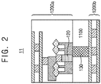
- FIG. 2 illustrates a BSPDN semiconductor architecture according to a related embodiment.
- the semiconductor architecture 11 may include a wafer 1100, a first semiconductor device 1200a provided on a first surface of the wafer 1100, and a second semiconductor device 1200b provided on a second surface of the wafer 1100.
- the first semiconductor device 1200a may be an integrated circuit for signal routing including components such as, for example, active transistors, signal wires, and BPRs 120, etc.
- the active transistors may include a power tapping epitaxial layer and a non-power tapping epitaxial layer.
- the signal wires are connected to the non-power tapping epitaxial layer of the active transistors for signal routing between the active transistors.
- the BPRs 120 are connected to the power tapping epitaxial layer of the active transistors and are not connected to the signal wires.
- the BPRs 120 are respectively configured to deliver power to the active transistors.
- the second semiconductor device 1200b may be a PDN integrated circuit.
- a TSV 130 configured as a power connecting structure may protrude from the semiconductor device 1200b.
- the BPR 120 included in the first semiconductor device 1200a and the TSV 130 protruding from the second semiconductor device 1200b may be misaligned with each other.
- the misalignment between the BPR 120 and the TSV 130 may increase the resistance of the semiconductor architecture 11 and may lead to a device failure of the semiconductor architecture 11.
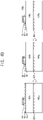
- FIGS. 3A through 3D illustrate a method of manufacturing a BSPDN semiconductor architecture according to a related embodiment.
- the method may include providing a wafer 1100 including a sacrificial layer 1100a, an etch stop layer 1500, and a carrier substrate 1100b.
- the sacrificial layer 1100a may be a silicon (Si) bulk layer
- the carrier substrate 1100b may be a Si layer.
- the etch stop layer 1500 may be provided between the sacrificial layer 1100a and the carrier substrate 1100b.
- a first semiconductor device 1200a may be provided on a first surface of the carrier substrate 1100b.
- the first semiconductor device 1200a may be an integrated circuit including components such as, for example, active transistors, signal wires, and BPRs 120.
- the BPR 120 may be provided on a first surface of the carrier substrate 1100b.
- a wafer-to-wafer bonding process may be carried out.
- a second wafer 1300 may be provided on a first surface of the first semiconductor device 1200a.
- the second wafer 1300 may be bonded by an adhesive layer 1400 provided between the first semiconductor device 1200a and the second wafer 1300.
- the wafer-to-wafer bonded semiconductor architecture is flipped.
- the sacrificial layer 1100a may be removed, and the etch stop layer 1500 may be removed to expose the second surface of the carrier substrate 1100b.
- a second semiconductor device 1200b may be provided on the exposed second surface of the carrier substrate 1 100b.
- the second semiconductor device 1200b may be a PDN integrated circuit with, for example, a TSV 130 protruding from a first surface of the second semiconductor device 1200b.
- the TSV 130 may be formed to penetrate the carrier substrate 1100b.
- the second semiconductor device 1200b may be provided on the second surface of the carrier substrate 1100b based on a location of the BPR 120 included in the first semiconductor device 1200a to land on the BPR 120.
- a misalignment may occur between the TSV 130 and the BPR 120 because it is difficult to accurately detect a location of the BPR 120 during a TSV 130 landing process when integrating the second semiconductor device 1200b on a second side of the carrier substrate 1100b. Due to the misalignment between the TSV 130 and the BPR 120 which results in a misalignment between the first semiconductor device 1200a and the second semiconductor device 1200b, a resistance of the semiconductor architecture 11 may increase. In addition, the misalignment between the first semiconductor device 1200a and the second semiconductor device 1200b may lead to a failure of the semiconductor architecture 11.
- FIG. 4 illustrates a perspective view of a BSPDN semiconductor architecture according to an example embodiment.
- the BSPDN semiconductor architecture 1 may include a wafer 100, a first semiconductor device 200a provided on a first surface of the wafer 100, and a second semiconductor device 200b provided on a second surface of the wafer 100 opposite to the first semiconductor device 200a.
- the first semiconductor device 200a and the second semiconductor device 200b may be integrated to each other and may form a BSPDN semiconductor architecture 1.
- the wafer 100 may include, for example, a Si substrate, a glass substrate, a sapphire substrate, etc. However, embodiments are not limited thereto. As illustrated in FIG. 3 , the wafer 100 may be a circular panel, but the shape of the wafer 100 is not limited thereto. For example, the wafer 100 may be a tetragonal panel. The wafer 100 may include a single layer or multiple layers.
- FIG. 5 illustrates a cross-sectional view taken along line I-I' of FIG. 4 according to an example embodiment.
- the example BSPDN semiconductor architecture 1 includes a first semiconductor device 200a provided on a first surface of the wafer 100 and a second semiconductor device 200b provided on a second surface of the wafer 100.
- the first semiconductor device 200a may be an integrated circuit including components such as, for example, active transistors, signal wires, and BPRs 20, etc.
- the BPR 20 may be provided to face the first surface of the wafer 100.
- the active transistors may include a power tapping epitaxial layer and a non-power tapping epitaxial layer.
- the signal wires are connected to the non-power tapping epitaxial layer of the active transistors for signal routing between the active transistors.
- the BPRs 120 are connected to the power tapping epitaxial layer of the active transistors and are not connected to the signal wires.
- the BPRs 120 are respectively configured to deliver power to the active transistors.
- the second semiconductor device 200b may be a PDN integrated circuit.
- a TSV 30 configured as a power connecting structure may be formed to protrude from a first surface of the second semiconductor device 200b and penetrate the wafer 100.
- the BSPDN semiconductor architecture 1 also includes a landing pad 60.
- the landing pad 60 is provided between the BPR 20 and the TSV 30.
- the landing pad 60 may be covered by a TSV etch stop layer 40 and an encapsulant 50.
- a second surface of the landing pad 60 may be covered by a TSV etch stop layer 40 and the first surface and the side surfaces of the landing pad 60 may be covered or encapsulated by an encapsulant 50.
- embodiments are not limited thereto.
- the landing pad 60 may have a rectangular shape from a cross-sectional view and have flat first and second surfaces, but shapes of the landing pad 60 are not limited thereto.
- the landing pad 60 may be formed of metal having a relatively low resistance.
- the landing pad 60 may be formed of copper (Cu), cobalt (Co), ruthenium (Ru), etc. However, embodiments are not limited thereto.
- a width of the landing pad 60 may be greater than a width of the BPR 20 and a width of the TSV 30, but embodiments are not limited thereto.
- the alignment between the BPR 20 and the TSV 30 may be improved as compared to the related embodiment by providing the landing pad 60 which is included in the wafer 100 prior to providing the BPR 20 and the TSV 30. Accordingly, the first semiconductor device 200a and the second semiconductor device 200b may be more accurately aligned with each other as compared to the related embodiment. Based on the improved alignment of the first semiconductor device 200a and the second semiconductor device 200b, the integration and performance of the BSPDN semiconductor architecture 1 may be improved. Further, by providing semiconductor devices on both of the first surface of the wafer 100 and the second surface of the wafer 100, the area and the resistance of the BSPDN semiconductor architecture 1 may be reduced.
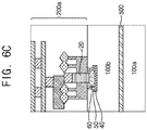
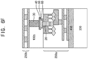
- FIGS. 6A through 6F illustrate a method of manufacturing a BSPDN semiconductor architecture according to an example embodiment.
- the method includes providing a wafer 100 including a sacrificial layer 100a, an etch stop layer 500, and a carrier substrate 100b.
- the sacrificial layer 100a may be a Si bulk layer.
- the etch stop layer 500 may be provided on the sacrificial layer 100a.
- the etch stop layer 500 may be provided by an epitaxial growth of silicon germanium (SiGe) on the sacrificial layer 100a.
- SiGe silicon germanium
- the etch stop layer 500 may be an oxide layer in a silicon-on-insulator (SOI) wafer.
- the carrier substrate 100b may include, for example, a Si substrate, a glass substrate, a sapphire substrate, etc. However, embodiments are not limited thereto.
- a TSV etch stop layer 40 is provided on a first surface of the carrier substrate 100b.
- a landing pad 60 is formed on a first surface of the TSV etch stop layer 40 by depositing and patterning a metal material.
- the metal material of the landing pad 60 may be a material having a relatively low resistance such as, for example, Cu, Co, Ru, etc. However, embodiments are not limited thereto.
- the landing pad 60 may have a rectangular shape from a cross-sectional view and have flat first and second surface. However, embodiments are not limited thereto and the landing pad 60 may have various shapes.
- An encapsulant 50 may be provided on the landing pad 60 and the first surface of the TSV etch stop layer 40 to protect the landing pad 60.
- the encapsulant 50 may encapsulate the landing pad 60 and the first surface of the TSV etch stop layer 40.
- the encapsulant 50 may be formed of epoxy resin, silica, etc. However, materials of the encapsulant 50 are not limited thereto.
- the encapsulant 50 and the TSV etch stop layer 40 may be removed in areas other than in the area covering the first surface and side surfaces of the landing pad 60 to expose the first surface of the carrier substrate 100b.
- the encapsulant 50 and the TSV etch stop layer 40 may be removed by, for example, patterned etching. However, embodiments are not limited thereto.
- a substrate layer 100b' may be provided on the landing pad 60 and the exposed first surface of the carrier substrate 100b.
- the substrate layer 100b' may be, for example, a Si layer.
- the substrate layer 100b' may be provided to carry out, for example, a front-end-of-line (FEOL) and middle-end-of-line (MEOL) integration in a first semiconductor device 200a.
- FEOL front-end-of-line
- MEOL middle-end-of-line
- the carrier substrate 100b and the substrate layer 100b' may be integrally formed, and may be together referred to as the carrier substrate 100b.
- a first semiconductor device 200a may be provided on a first surface of the carrier substrate 100b.
- the first semiconductor device 200a may be an integrated circuit including components such as, for example, active transistors, signal wires, and BPRs 20, etc.
- the BPR 20 may be provided on a first surface of the carrier substrate 100b to be in contact with the landing pad 60 based on a location of the landing pad 60.
- the location of the landing pad 60 may be detected based on a preset alignment key, but embodiments are not limited thereto.
- the landing pad 60 may have a greater width than a width of the BPR 20, but embodiments are not limited thereto.
- a width of the BPR 20 may range from around 5 nm to 30 nm.
- a width of the BPR 20 is not limited thereto. Based on the width of the landing pad 60 being greater than the width of the BPR 20, aligning and connecting the BPR 20 with the landing pad 60 may be facilitated during a manufacturing process.
- the size and shape of the landing pad 60 is not limited by shape and size of the BPR 20 which may facilitate the manufacturing process of the landing pad 60.
- a wafer-to-wafer bonding process may be carried out.
- a second wafer 300 may be provided on a first surface of the first semiconductor device 200a.
- the second wafer 300 may be bonded to the first semiconductor device 200a by providing an adhesive layer 400 between the first semiconductor device 200a and the second wafer 300.
- the second wafer 300 may be directly provided on the first semiconductor device 200a.
- the second wafer 300 may be directly bonded to the first semiconductor device 200a by a Si direct bonding without using an adhesive layer.
- the wafer-to-wafer bonded semiconductor architecture may be flipped.
- the sacrificial layer 100a may be removed, and the etch stop layer 500 may be removed to expose the second surface of the carrier substrate 100b.
- the sacrificial layer 100a and the etch stop layer 500 may be removed by a grinding process including, for example, chemical-mechanical polishing (CMP) or dry etching.
- CMP chemical-mechanical polishing
- embodiments are not limited thereto.
- a second semiconductor device 200b may be provided on the second surface of the carrier substrate 100b.
- the second semiconductor device 200b may be a PDN integrated circuit with, for example, a TSV 30 protruding from a first surface of the second semiconductor device 200b.
- the TSV 30 may be formed to penetrate the carrier substrate 100b to contact the landing pad 60 based on a location of the landing pad 60.
- the location of the landing pad 60 may be detected based on the preset alignment key, but embodiments are not limited thereto.
- the landing pad 60 may have a greater width than a width of the TSV 30, but embodiments are not limited thereto.
- a width of the TSV 30 may range around 50 nm to 100 nm.
- a width of the TSV 30 is not limited thereto. Based on the width of the landing pad 60 being greater than the width of the TSV 30, aligning and connecting the TSV 30 to the landing pad 60 may be easier. As the TSV 30 is better aligned with the landing pad 60 which is connected to the BPR 20, the alignment between the TSV 30 and the BPR 20 may be improved. In addition, even when surfaces of the BPR 20 and the TSV 30 are not fully in contact with the landing pad 60, the connectivity of the BPR 20 and TSV 30 may be improved by being connected through the metal landing pad 60.
- the resistance of the BSPDN semiconductor architecture 1 may be reduced and the IR drop may be improved.
- the first semiconductor device 200a and the second semiconductor device 200b may be more accurately aligned and connected with each other to improve the performance of the BSPDN semiconductor architecture 1.
- the integration and the performance of the BSPDN semiconductor architecture 1 may be improved.
- moving the PDN semiconductor device from the first side to the second side of the wafer 100 may reduce the size and resistance of the BSPDN semiconductor architecture 1.
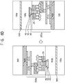
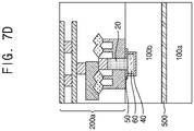
- FIGS. 7A through 7G illustrate a method of manufacturing a BSPDN semiconductor architecture 1 according to another example embodiment.
- the method includes providing a wafer 100 including a sacrificial layer 100a, an etch stop layer 500, and a carrier substrate 100b.
- the sacrificial layer 100a may be a Si bulk layer.
- the etch stop layer 500 may be provided on the sacrificial layer 100a.
- the etch stop layer 500 may be provided by an epitaxial growth of silicon germanium (SiGe) on the sacrificial layer 100a.
- SiGe silicon germanium
- the etch stop layer 500 may be an oxide layer in a silicon-on-insulator (SOI) wafer.
- SOI silicon-on-insulator
- the wafer 100 may include, for example, a Si substrate, a glass substrate, a sapphire substrate, etc. However, embodiments are not limited thereto.
- a trench 70 is provided on the carrier substrate 100b.
- the trench 70 may be provided by etching the carrier substrate 100b and may have a rectangular shape from a cross-sectional view.
- embodiments are not limited thereto.
- a TSV etch stop layer 40 is provided on a top surface of the carrier substrate 100b and the trench 70.
- the TSV etch stop layer 40 may be provided to cover the top surface of the carrier substrate 100b and the trench 70.
- a metal material 60' is provided on the carrier substrate 100b and the trench 70.
- the metal material 60' may fill the trench 70.
- the metal material 60' may be a material having a relatively low resistance such as, for example, Cu, Co, Ru, etc. However, embodiment are not limited thereto.
- the metal material 60' and the TSV etch stop layer 40 may be removed in areas other than the area of a first surface of the trench 70 filled with the metal material 60' to form the landing pad 60 and to expose the first surface of the carrier substrate 100b.
- the first surface of the landing pad 60 is coplanar to the exposed first surface of the carrier substrate 100b.
- the metal material 60' and the TSV etch stop layer 40 may be removed by a grinding process such as, for example, CMP or dry etching.
- the shape of the landing pad 60 corresponds to the shape of the trench 70, the landing pad 60 may have a rectangular shape. However, embodiments are not limited thereto.
- an encapsulant 50 may be provided on an area of the landing pad 60.
- the encapsulant 50 may cover the landing pad 60 and have a greater size than the landing pad 60 from a plan view.
- the encapsulant 50 may include epoxy resin, silica, etc., but materials of the encapsulant 50 are not limited thereto.
- a substrate layer 100b' may be provided on the landing pad 60 and the exposed first surface of the carrier substrate 100b.
- the substrate layer 100b' may be, for example, a Si layer.
- the substrate layer 100b' may be provided to carry out, for example, a FEOL and a MEOL process.
- the carrier substrate 100b and the substrate layer 100b' may be integrally formed, and may be together referred to as the carrier substrate 100b.
- a first semiconductor device 200a may be provided on a first surface of the carrier substrate 100b.
- the first semiconductor device 200a may be an integrated circuit including components such as, for example, active transistors, signal wires, BPRs 20, etc.
- the BPR 20 may be provided on a first surface of the carrier substrate 100b to be in contact with the landing pad 60 based on a location of the landing pad 60.
- the location of the landing pad 60 may be detected based on a preset alignment key, but embodiments are not limited thereto.
- the landing pad 60 may have a greater width than a width of the BPR 20, but embodiments are not limited thereto.
- a width of the BPR 20 may range from around 5 nm to 30 nm.
- a width of the BPR 20 is not limited thereto. Based on the width of the landing pad 60 being greater than the width of the BPR 20, aligning and connecting the BPR 20 to the landing pad 60 may be easier.
- the size and shape of the landing pad 60 is not necessarily limited by the size and shape of the BPR 20, and thus, a manufacturing process of the landing pad 60 may be facilitated.
- a wafer-to-wafer bonding process may be carried out.
- a second wafer 300 may be provided on a first surface of the first semiconductor device 200a.
- the second wafer 300 may be bonded to the first semiconductor device 200a by providing an adhesive layer 400 between the first semiconductor device 200a and the second wafer 300.
- the second wafer 300 may be directly provided on the first semiconductor device 200a.
- the second wafer 300 may be directly bonded to the first semiconductor device 200a by a Si direct bonding without using an adhesive layer.
- the wafer-to-wafer bonded semiconductor architecture may be flipped.
- the sacrificial layer 100a may be removed, and the etch stop layer 500 may be removed to expose the second surface of the carrier substrate 100b.
- the sacrificial layer 100a and the etch stop layer 500 may be removed by a grinding process including, for example, CMP or dry etching, but embodiments are not limited thereto.
- a second semiconductor device 200b may be provided on the second surface of the carrier substrate 100b.
- the second semiconductor device 200b may be a PDN integrated circuit with, for example, a TSV 30 protruding from a first surface of the second semiconductor device 200b.
- the TSV 30 may be formed to penetrate the carrier substrate 100b and land on the landing pad 60 based on the location of the landing pad 60.
- the location of the landing pad 60 may be detected based on the preset alignment key, but embodiments are not limited thereto.
- the landing pad 60 may have a greater width than a width of the TSV 30, but embodiments are not limited thereto.
- a width of the TSV 30 may range around 50 nm to 100 nm.
- a width of the TSV 30 is not limited thereto.
- aligning and connecting the TSV 30 to the landing pad 60 may be easier.
- the alignment between the TSV 30 and the BPR 20 may be improved.
- the connectivity of the BPR 20 and TSV 30 may be improved based on being connected through the metal landing pad 60.
- the resistance of the BSPDN semiconductor architecture 1 may be reduced and the IR drop may be improved.
- the first semiconductor device 200a and the second semiconductor device 200b may be more accurately aligned with and connected to each other.
- the integration and performance of the semiconductor architecture 1 may be improved.
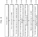
- FIG. 8 illustrates a flowchart of a method of manufacturing a BSPDN semiconductor architecture according to an example embodiment.
- a wafer may be provided (S110).
- the wafer may include a sacrificial layer, an etch stop layer, and a carrier substrate.
- the sacrificial layer may be a Si bulk layer.
- the etch stop layer may be provided on the sacrificial layer by an epitaxial growth of silicon germanium (SiGe) on the sacrificial layer, but embodiments are not limited thereto.
- the etch stop layer may be an oxide layer in a silicon-on-insulator (SOI) wafer.
- the carrier substrate may include, for example, a Si substrate, a glass substrate, a sapphire substrate, etc.
- a landing pad is formed in the wafer (S120).
- the landing pad may be formed by depositing and patterning a metal material on the carrier substrate, as described in more detail with reference to FIGS. 9 and 10 .
- a substrate is provided on the carrier substrate (S130).
- the substrate may be a Si layer and may be integrally formed with the carrier substrate.
- a first semiconductor device may be provided on the carrier substrate (S140).
- the first semiconductor device may be an integrated circuit including components such as, for example, active transistors, signal wires, and BPRs.
- the BPR may be provided on a first surface of the carrier substrate to be in contact with the landing pad based on a location of the landing pad.
- a second wafer may be provided on the first semiconductor device (S 150).
- the second wafer may be bonded to the first semiconductor device by providing an adhesive layer between the first semiconductor device and the second wafer.
- the second wafer may be directly provided on the first semiconductor device by, for example, a Si direct bonding without using an adhesive layer.
- the wafer-to-wafer bonded semiconductor architecture may be flipped.
- the sacrificial layer and the etch stop layer may be removed (S150).
- the etch stop layer may be removed to expose the second surface of the carrier substrate.
- the sacrificial layer and the etch stop layer may be removed by a grinding process such as, for example, CMP or dry etching, but embodiments are not limited thereto.
- a second semiconductor device may be provided on the second surface of the carrier substrate (S170).
- the second semiconductor device may be a PDN integrated circuit with, for example, a TSV protruding from a first surface of the second semiconductor device.
- the TSV may be formed to penetrate the carrier substrate to be in contact with the landing pad based on the location of the landing pad.
- the alignment and connectivity between the BPR and the TSV may be improved, and the resistance of the BSPDN semiconductor architecture 1 may be reduced.
- performance of the semiconductor architecture may be improved.
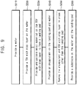
- FIG. 9 illustrates a flowchart of a method of manufacturing a landing pad in a semiconductor wafer according to an example embodiment.
- a wafer including a sacrificial layer, an etch stop layer, and a carrier substrate is provided (S210).
- a TSV etch stop layer may be provided on a first surface of the wafer (S220).
- a metal material is deposited and patterned on the TSV etch stop layer to form a landing pad (S230).
- the landing pad may have a rectangular shape.
- An encapsulant is provided on the landing pad and the first surface of the carrier wafer (S240).
- the encapsulant and the TSV etch stop layer are removed in areas other than in the area covering the first surface and side surfaces of the landing pad (S250).
- the encapsulant and TSV etch stop layer may be etched to expose the first surface of the wafer.
- a substrate is provided on the wafer and the landing pad (S260).
- the substrate may be a Si layer and may be integrally formed with the carrier substrate.
- FIG. 10 illustrates a flowchart of a method of manufacturing a landing pad in a semiconductor wafer according to another example embodiment.
- a wafer including a sacrificial layer, an etch stop layer, and a carrier substrate is provided (S310).
- a trench may be formed in the wafer (S320). The trench may be etched and may have a rectangular shape.
- a TSV etch stop layer may be provided on the first surface of the wafer and the trench (S330).
- a metal material may be provided on the first surface of the wafer and fill the trench (S340). The metal material and the TSV etch stop layer may be removed in areas other than the area of a first surface of the trench filled with the metal material to form the landing pad (S350).
- the metal material and the TSV etch stop layer may be removed by, for example, CMP or dry etching.
- An encapsulant is provided on an area of the landing pad (S360).
- a size of the encapsulant may be greater than a size of the landing pad from a plan view.
- a substrate is provided on the wafer and the landing pad (S370). The substrate may be a Si layer and may be integrally formed with the carrier substrate.
- a size and shape of the landing pad may not be limited by a size and shape of components of the semiconductor devices such as, for example, a BPR, a TSV, etc.
- FIG. 11 illustrates a semiconductor package that may incorporate the BSPDN semiconductor architectures according to example embodiments.
- a semiconductor package 2000 may include a processor 2200 and semiconductor devices 2300 that are mounted on a substrate 2100.
- the processor 2200 and/or the semiconductor devices 2300 may include one or more of BSPDN semiconductor architecture 1 described in the above example embodiments.
- FIG. 12 illustrates a schematic block diagram of an electronic system according to an example embodiment.
- an electronic system 3000 in accordance with an embodiment may include a microprocessor 3100, a memory 3200, and a user interface 3300 that perform data communication using a bus 3400.
- the microprocessor 3100 may include a central processing unit (CPU) or an application processor (AP).
- the electronic system 3000 may further include a random access memory (RAM) 3500 in direct communication with the microprocessor 3100.
- the microprocessor 3100 and/or the RAM 3500 may be implemented in a single module or package.
- the user interface 3300 may be used to input data to the electronic system 3000, or output data from the electronic system 3000.
- the user interface 3300 may include a keyboard, a touch pad, a touch screen, a mouse, a scanner, a voice detector, a liquid crystal display (LCD), a micro light-emitting device (LED), an organic light-emitting diode (OLED) device, an active-matrix light-emitting diode (AMOLED) device, a printer, a lighting, or various other input/output devices without limitation.
- the memory 3200 may store operational codes of the microprocessor 3100, data processed by the microprocessor 3100, or data received from an external device.
- the memory 3200 may include a memory controller, a hard disk, or a solid state drive (SSD).
- At least the microprocessor 3100, the memory 3200 and/or the RAM 3500 in the electronic system 3000 may include BSPDN semiconductor architecture 1 as described in the above example embodiments.
Landscapes
- Internal Circuitry In Semiconductor Integrated Circuit Devices (AREA)
- Physics & Mathematics (AREA)
- Geometry (AREA)
Applications Claiming Priority (2)
| Application Number | Priority Date | Filing Date | Title |
|---|---|---|---|
| US202063113631P | 2020-11-13 | 2020-11-13 | |
| US17/159,972 US11769728B2 (en) | 2020-11-13 | 2021-01-27 | Backside power distribution network semiconductor package and method of manufacturing the same |
Publications (2)
| Publication Number | Publication Date |
|---|---|
| EP4002435A1 true EP4002435A1 (fr) | 2022-05-25 |
| EP4002435B1 EP4002435B1 (fr) | 2025-06-04 |
Family
ID=76197252
Family Applications (1)
| Application Number | Title | Priority Date | Filing Date |
|---|---|---|---|
| EP21176650.6A Active EP4002435B1 (fr) | 2020-11-13 | 2021-05-28 | Dispositif semi-conducteur avec réseau de distribution de puissance arrière et son procédé de fabrication |
Country Status (5)
| Country | Link |
|---|---|
| US (2) | US11769728B2 (fr) |
| EP (1) | EP4002435B1 (fr) |
| KR (1) | KR20220065651A (fr) |
| CN (1) | CN114496954A (fr) |
| TW (1) | TWI881129B (fr) |
Cited By (1)
| Publication number | Priority date | Publication date | Assignee | Title |
|---|---|---|---|---|
| EP4254491A1 (fr) * | 2022-03-31 | 2023-10-04 | Samsung Electronics Co., Ltd. | Dispositif semi-conducteur |
Families Citing this family (12)
| Publication number | Priority date | Publication date | Assignee | Title |
|---|---|---|---|---|
| US11925033B2 (en) * | 2021-03-30 | 2024-03-05 | Taiwan Semiconductor Manufacturing Company, Ltd. | Embedded backside memory on a field effect transistor |
| US20220336355A1 (en) * | 2021-04-19 | 2022-10-20 | Samsung Electronics Co., Ltd. | Thermal budget enhanced buried power rail and method of manufacturing the same |
| US12261116B2 (en) * | 2021-08-05 | 2025-03-25 | Taiwan Semiconductor Manufacturing Company, Ltd. | Backside signal routing |
| US11990412B2 (en) * | 2021-09-29 | 2024-05-21 | International Business Machines Corporation | Buried power rails located in a base layer including first, second, and third etch stop layers |
| US20230170395A1 (en) * | 2021-11-30 | 2023-06-01 | International Business Machines Corporation | CROSS CELL LOCAL INTERCONNECT WITH BPR AND CBoA |
| US20230299000A1 (en) * | 2022-03-17 | 2023-09-21 | International Business Machines Corporation | Method and structure for forming landing for backside power distribution network |
| US12550370B2 (en) * | 2022-04-25 | 2026-02-10 | Taiwan Semiconductor Manufacturing Company, Ltd. | Semiconductor device and manufacturing method thereof |
| US20230378138A1 (en) * | 2022-05-20 | 2023-11-23 | Tokyo Electron Limited | Sequential complimentary fet incorporating backside power distribution network through wafer bonding prior to formation of active devices |
| US20230377983A1 (en) * | 2022-05-20 | 2023-11-23 | Tokyo Electron Limited | Method to reduce parasitic resistance for cfet devices through single damascene processing of vias |
| CN119522486A (zh) * | 2022-05-20 | 2025-02-25 | 东京毅力科创株式会社 | 在形成有源器件之前通过晶片键合来结合背面电力分配网络的顺序互补型fet |
| US12532732B2 (en) | 2022-10-11 | 2026-01-20 | Samsung Electronics Co., Ltd. | Semiconductor device |
| US20250087527A1 (en) * | 2023-09-13 | 2025-03-13 | International Business Machines Corporation | Handler wafer with low overlay residual backside patterning |
Citations (5)
| Publication number | Priority date | Publication date | Assignee | Title |
|---|---|---|---|---|
| US20160284731A1 (en) * | 2015-02-04 | 2016-09-29 | Texas Instruments Incorporated | Efficient buried oxide layer interconnect scheme |
| EP3324436A1 (fr) * | 2016-11-21 | 2018-05-23 | IMEC vzw | Puce de circuit intégré avec réseau de distribution électrique sur la face arrière de la puce |
| US20200135634A1 (en) * | 2018-10-26 | 2020-04-30 | Taiwan Semiconductor Manufacturing Company, Ltd. | Buried Power Rail and Method Forming Same |
| EP3671859A1 (fr) * | 2018-12-20 | 2020-06-24 | IMEC vzw | Procédé de transistor à effet de champ à grille isolée vertical intégré dans une puce semiconductrice |
| US20200279811A1 (en) * | 2019-03-01 | 2020-09-03 | Samsung Electronics Co., Ltd. | Apparatus and method of forming backside buried conductor in integrated circuit |
Family Cites Families (10)
| Publication number | Priority date | Publication date | Assignee | Title |
|---|---|---|---|---|
| EP2378549A1 (fr) | 2010-04-06 | 2011-10-19 | S.O.I.Tec Silicon on Insulator Technologies | Procédé de fabrication d'un substrat semi-conducteur |
| US8921976B2 (en) | 2011-01-25 | 2014-12-30 | Stmicroelectronics, Inc. | Using backside passive elements for multilevel 3D wafers alignment applications |
| KR20150061161A (ko) * | 2013-11-26 | 2015-06-04 | 삼성전자주식회사 | 실리콘-관통 비아들을 갖는 반도체 칩, 이를 포함하는 반도체 패키지, 및 이들의 제조 방법 |
| US10475692B2 (en) | 2017-04-07 | 2019-11-12 | Globalfoundries Inc. | Self aligned buried power rail |
| US10586765B2 (en) * | 2017-06-22 | 2020-03-10 | Tokyo Electron Limited | Buried power rails |
| US11094594B2 (en) | 2017-09-12 | 2021-08-17 | Mediatek Inc. | Semiconductor structure with buried power rail, integrated circuit and method for manufacturing the semiconductor structure |
| US10700207B2 (en) * | 2017-11-30 | 2020-06-30 | Taiwan Semiconductor Manufacturing Company Ltd. | Semiconductor device integrating backside power grid and related integrated circuit and fabrication method |
| US11133254B2 (en) * | 2018-09-28 | 2021-09-28 | Taiwan Semiconductor Manufacturing Company, Ltd. | Hybrid power rail structure |
| US11063041B2 (en) * | 2018-10-31 | 2021-07-13 | Taiwan Semiconductor Manufacturing Co., Ltd. | Integrated circuit device including a power supply line and method of forming the same |
| US10878162B2 (en) * | 2018-10-31 | 2020-12-29 | Taiwan Semiconductor Manufacturing Company Ltd. | Metal with buried power for increased IC device density |
-
2021
- 2021-01-27 US US17/159,972 patent/US11769728B2/en active Active
- 2021-05-20 KR KR1020210064697A patent/KR20220065651A/ko not_active Ceased
- 2021-05-27 TW TW110119200A patent/TWI881129B/zh active
- 2021-05-28 EP EP21176650.6A patent/EP4002435B1/fr active Active
- 2021-06-15 CN CN202110659197.XA patent/CN114496954A/zh active Pending
-
2023
- 2023-08-28 US US18/457,000 patent/US12142564B2/en active Active
Patent Citations (5)
| Publication number | Priority date | Publication date | Assignee | Title |
|---|---|---|---|---|
| US20160284731A1 (en) * | 2015-02-04 | 2016-09-29 | Texas Instruments Incorporated | Efficient buried oxide layer interconnect scheme |
| EP3324436A1 (fr) * | 2016-11-21 | 2018-05-23 | IMEC vzw | Puce de circuit intégré avec réseau de distribution électrique sur la face arrière de la puce |
| US20200135634A1 (en) * | 2018-10-26 | 2020-04-30 | Taiwan Semiconductor Manufacturing Company, Ltd. | Buried Power Rail and Method Forming Same |
| EP3671859A1 (fr) * | 2018-12-20 | 2020-06-24 | IMEC vzw | Procédé de transistor à effet de champ à grille isolée vertical intégré dans une puce semiconductrice |
| US20200279811A1 (en) * | 2019-03-01 | 2020-09-03 | Samsung Electronics Co., Ltd. | Apparatus and method of forming backside buried conductor in integrated circuit |
Cited By (2)
| Publication number | Priority date | Publication date | Assignee | Title |
|---|---|---|---|---|
| EP4254491A1 (fr) * | 2022-03-31 | 2023-10-04 | Samsung Electronics Co., Ltd. | Dispositif semi-conducteur |
| US12598978B2 (en) | 2022-03-31 | 2026-04-07 | Samsung Electronics Co., Ltd. | Semiconductor device having a source/drain contact connected to a back-side power rail by a landing pad and a through electrode |
Also Published As
| Publication number | Publication date |
|---|---|
| TW202220152A (zh) | 2022-05-16 |
| US11769728B2 (en) | 2023-09-26 |
| US20230411294A1 (en) | 2023-12-21 |
| TWI881129B (zh) | 2025-04-21 |
| US20220157723A1 (en) | 2022-05-19 |
| KR20220065651A (ko) | 2022-05-20 |
| US12142564B2 (en) | 2024-11-12 |
| CN114496954A (zh) | 2022-05-13 |
| EP4002435B1 (fr) | 2025-06-04 |
Similar Documents
| Publication | Publication Date | Title |
|---|---|---|
| EP4002435B1 (fr) | Dispositif semi-conducteur avec réseau de distribution de puissance arrière et son procédé de fabrication | |
| US12272730B2 (en) | Transistor level interconnection methodologies utilizing 3D interconnects | |
| US12125788B2 (en) | Through silicon buried power rail implemented backside power distribution network semiconductor architecture and method of manufacturing the same | |
| US12557677B2 (en) | Backside power distribution network semiconductor architecture using direct epitaxial layer connection and method of manufacturing the same | |
| US10014285B2 (en) | Semiconductor devices | |
| EP4227994A1 (fr) | Empilement de puces qui partagent leurs rails d'alimentation | |
| JP2025504616A (ja) | 埋め込み電源配線を有する半導体構造体 | |
| US20240429169A1 (en) | Thermal budget enhanced buried power rail and method of manufacturing the same | |
| US12068256B2 (en) | Method of manufacturing a three dimensional integrated semiconductor architecture having alignment marks provided in a carrier substrate | |
| US20230326858A1 (en) | Reversed high aspect ratio contact (harc) structure and process | |
| CN116895634A (zh) | 半导体芯片架构及其制造方法 | |
| EP4261882A1 (fr) | Structure inversée et procédé de contact à rapport de forme élevé (harc) | |
| US20240379596A1 (en) | Conductive pad on a through-silicon via | |
| CN116581103A (zh) | 三维堆叠半导体芯片架构和制造其的方法 | |
| KR20240111224A (ko) | 후면 배전 네트워크 반도체 패키지 및 그의 제조 방법 | |
| TW202612154A (zh) | 高效率微裝置 |
Legal Events
| Date | Code | Title | Description |
|---|---|---|---|
| PUAI | Public reference made under article 153(3) epc to a published international application that has entered the european phase |
Free format text: ORIGINAL CODE: 0009012 |
|
| STAA | Information on the status of an ep patent application or granted ep patent |
Free format text: STATUS: REQUEST FOR EXAMINATION WAS MADE |
|
| 17P | Request for examination filed |
Effective date: 20211129 |
|
| AK | Designated contracting states |
Kind code of ref document: A1 Designated state(s): AL AT BE BG CH CY CZ DE DK EE ES FI FR GB GR HR HU IE IS IT LI LT LU LV MC MK MT NL NO PL PT RO RS SE SI SK SM TR |
|
| P01 | Opt-out of the competence of the unified patent court (upc) registered |
Effective date: 20230520 |
|
| GRAP | Despatch of communication of intention to grant a patent |
Free format text: ORIGINAL CODE: EPIDOSNIGR1 |
|
| STAA | Information on the status of an ep patent application or granted ep patent |
Free format text: STATUS: GRANT OF PATENT IS INTENDED |
|
| INTG | Intention to grant announced |
Effective date: 20250327 |
|
| GRAS | Grant fee paid |
Free format text: ORIGINAL CODE: EPIDOSNIGR3 |
|
| GRAA | (expected) grant |
Free format text: ORIGINAL CODE: 0009210 |
|
| STAA | Information on the status of an ep patent application or granted ep patent |
Free format text: STATUS: THE PATENT HAS BEEN GRANTED |
|
| AK | Designated contracting states |
Kind code of ref document: B1 Designated state(s): AL AT BE BG CH CY CZ DE DK EE ES FI FR GB GR HR HU IE IS IT LI LT LU LV MC MK MT NL NO PL PT RO RS SE SI SK SM TR |
|
| REG | Reference to a national code |
Ref country code: GB Ref legal event code: FG4D |
|
| REG | Reference to a national code |
Ref country code: CH Ref legal event code: EP |
|
| REG | Reference to a national code |
Ref country code: DE Ref legal event code: R096 Ref document number: 602021031628 Country of ref document: DE |
|
| REG | Reference to a national code |
Ref country code: IE Ref legal event code: FG4D |
|
| REG | Reference to a national code |
Ref country code: NL Ref legal event code: FP |
|
| PG25 | Lapsed in a contracting state [announced via postgrant information from national office to epo] |
Ref country code: ES Free format text: LAPSE BECAUSE OF FAILURE TO SUBMIT A TRANSLATION OF THE DESCRIPTION OR TO PAY THE FEE WITHIN THE PRESCRIBED TIME-LIMIT Effective date: 20250604 Ref country code: FI Free format text: LAPSE BECAUSE OF FAILURE TO SUBMIT A TRANSLATION OF THE DESCRIPTION OR TO PAY THE FEE WITHIN THE PRESCRIBED TIME-LIMIT Effective date: 20250604 |
|
| REG | Reference to a national code |
Ref country code: LT Ref legal event code: MG9D |
|
| PG25 | Lapsed in a contracting state [announced via postgrant information from national office to epo] |
Ref country code: NO Free format text: LAPSE BECAUSE OF FAILURE TO SUBMIT A TRANSLATION OF THE DESCRIPTION OR TO PAY THE FEE WITHIN THE PRESCRIBED TIME-LIMIT Effective date: 20250904 Ref country code: GR Free format text: LAPSE BECAUSE OF FAILURE TO SUBMIT A TRANSLATION OF THE DESCRIPTION OR TO PAY THE FEE WITHIN THE PRESCRIBED TIME-LIMIT Effective date: 20250905 |
|
| PG25 | Lapsed in a contracting state [announced via postgrant information from national office to epo] |
Ref country code: PL Free format text: LAPSE BECAUSE OF FAILURE TO SUBMIT A TRANSLATION OF THE DESCRIPTION OR TO PAY THE FEE WITHIN THE PRESCRIBED TIME-LIMIT Effective date: 20250604 |
|
| PG25 | Lapsed in a contracting state [announced via postgrant information from national office to epo] |
Ref country code: BG Free format text: LAPSE BECAUSE OF FAILURE TO SUBMIT A TRANSLATION OF THE DESCRIPTION OR TO PAY THE FEE WITHIN THE PRESCRIBED TIME-LIMIT Effective date: 20250604 |
|
| PG25 | Lapsed in a contracting state [announced via postgrant information from national office to epo] |
Ref country code: HR Free format text: LAPSE BECAUSE OF FAILURE TO SUBMIT A TRANSLATION OF THE DESCRIPTION OR TO PAY THE FEE WITHIN THE PRESCRIBED TIME-LIMIT Effective date: 20250604 |
|
| PG25 | Lapsed in a contracting state [announced via postgrant information from national office to epo] |
Ref country code: RS Free format text: LAPSE BECAUSE OF FAILURE TO SUBMIT A TRANSLATION OF THE DESCRIPTION OR TO PAY THE FEE WITHIN THE PRESCRIBED TIME-LIMIT Effective date: 20250904 |
|
| PG25 | Lapsed in a contracting state [announced via postgrant information from national office to epo] |
Ref country code: LV Free format text: LAPSE BECAUSE OF FAILURE TO SUBMIT A TRANSLATION OF THE DESCRIPTION OR TO PAY THE FEE WITHIN THE PRESCRIBED TIME-LIMIT Effective date: 20250604 |
|
| REG | Reference to a national code |
Ref country code: DE Ref legal event code: R079 Ref document number: 602021031628 Country of ref document: DE Free format text: PREVIOUS MAIN CLASS: H01L0021740000 Ipc: H10W0015000000 |
|
| PG25 | Lapsed in a contracting state [announced via postgrant information from national office to epo] |
Ref country code: PT Free format text: LAPSE BECAUSE OF FAILURE TO SUBMIT A TRANSLATION OF THE DESCRIPTION OR TO PAY THE FEE WITHIN THE PRESCRIBED TIME-LIMIT Effective date: 20251006 |
|
| REG | Reference to a national code |
Ref country code: AT Ref legal event code: MK05 Ref document number: 1801235 Country of ref document: AT Kind code of ref document: T Effective date: 20250604 |
|
| PG25 | Lapsed in a contracting state [announced via postgrant information from national office to epo] |
Ref country code: IS Free format text: LAPSE BECAUSE OF FAILURE TO SUBMIT A TRANSLATION OF THE DESCRIPTION OR TO PAY THE FEE WITHIN THE PRESCRIBED TIME-LIMIT Effective date: 20251004 |
|
| PG25 | Lapsed in a contracting state [announced via postgrant information from national office to epo] |
Ref country code: SM Free format text: LAPSE BECAUSE OF FAILURE TO SUBMIT A TRANSLATION OF THE DESCRIPTION OR TO PAY THE FEE WITHIN THE PRESCRIBED TIME-LIMIT Effective date: 20250604 Ref country code: AT Free format text: LAPSE BECAUSE OF FAILURE TO SUBMIT A TRANSLATION OF THE DESCRIPTION OR TO PAY THE FEE WITHIN THE PRESCRIBED TIME-LIMIT Effective date: 20250604 |
|
| PG25 | Lapsed in a contracting state [announced via postgrant information from national office to epo] |
Ref country code: CZ Free format text: LAPSE BECAUSE OF FAILURE TO SUBMIT A TRANSLATION OF THE DESCRIPTION OR TO PAY THE FEE WITHIN THE PRESCRIBED TIME-LIMIT Effective date: 20250604 |
|
| PG25 | Lapsed in a contracting state [announced via postgrant information from national office to epo] |
Ref country code: EE Free format text: LAPSE BECAUSE OF FAILURE TO SUBMIT A TRANSLATION OF THE DESCRIPTION OR TO PAY THE FEE WITHIN THE PRESCRIBED TIME-LIMIT Effective date: 20250604 |
|
| PG25 | Lapsed in a contracting state [announced via postgrant information from national office to epo] |
Ref country code: RO Free format text: LAPSE BECAUSE OF FAILURE TO SUBMIT A TRANSLATION OF THE DESCRIPTION OR TO PAY THE FEE WITHIN THE PRESCRIBED TIME-LIMIT Effective date: 20250604 Ref country code: SK Free format text: LAPSE BECAUSE OF FAILURE TO SUBMIT A TRANSLATION OF THE DESCRIPTION OR TO PAY THE FEE WITHIN THE PRESCRIBED TIME-LIMIT Effective date: 20250604 |
|
| PG25 | Lapsed in a contracting state [announced via postgrant information from national office to epo] |
Ref country code: IT Free format text: LAPSE BECAUSE OF FAILURE TO SUBMIT A TRANSLATION OF THE DESCRIPTION OR TO PAY THE FEE WITHIN THE PRESCRIBED TIME-LIMIT Effective date: 20250604 |
|
| REG | Reference to a national code |
Ref country code: DE Ref legal event code: R097 Ref document number: 602021031628 Country of ref document: DE |
|
| PLBE | No opposition filed within time limit |
Free format text: ORIGINAL CODE: 0009261 |
|
| STAA | Information on the status of an ep patent application or granted ep patent |
Free format text: STATUS: NO OPPOSITION FILED WITHIN TIME LIMIT |
|
| PG25 | Lapsed in a contracting state [announced via postgrant information from national office to epo] |
Ref country code: DK Free format text: LAPSE BECAUSE OF FAILURE TO SUBMIT A TRANSLATION OF THE DESCRIPTION OR TO PAY THE FEE WITHIN THE PRESCRIBED TIME-LIMIT Effective date: 20250604 |
|
| REG | Reference to a national code |
Ref country code: CH Ref legal event code: L10 Free format text: ST27 STATUS EVENT CODE: U-0-0-L10-L00 (AS PROVIDED BY THE NATIONAL OFFICE) Effective date: 20260416 |