EP4002441A2 - Elektronischer schaltkreis für eine hybride molekülverbindung - Google Patents
Elektronischer schaltkreis für eine hybride molekülverbindung Download PDFInfo
- Publication number
- EP4002441A2 EP4002441A2 EP21204895.3A EP21204895A EP4002441A2 EP 4002441 A2 EP4002441 A2 EP 4002441A2 EP 21204895 A EP21204895 A EP 21204895A EP 4002441 A2 EP4002441 A2 EP 4002441A2
- Authority
- EP
- European Patent Office
- Prior art keywords
- face
- electronic circuit
- bonding
- exposed
- test pad
- Prior art date
- Legal status (The legal status is an assumption and is not a legal conclusion. Google has not performed a legal analysis and makes no representation as to the accuracy of the status listed.)
- Pending
Links
Images


Classifications
-
- H—ELECTRICITY
- H10—SEMICONDUCTOR DEVICES; ELECTRIC SOLID-STATE DEVICES NOT OTHERWISE PROVIDED FOR
- H10P—GENERIC PROCESSES OR APPARATUS FOR THE MANUFACTURE OR TREATMENT OF DEVICES COVERED BY CLASS H10
- H10P74/00—Testing or measuring during manufacture or treatment of wafers, substrates or devices
- H10P74/27—Structural arrangements therefor
- H10P74/273—Interconnections for measuring or testing, e.g. probe pads
-
- H—ELECTRICITY
- H10—SEMICONDUCTOR DEVICES; ELECTRIC SOLID-STATE DEVICES NOT OTHERWISE PROVIDED FOR
- H10P—GENERIC PROCESSES OR APPARATUS FOR THE MANUFACTURE OR TREATMENT OF DEVICES COVERED BY CLASS H10
- H10P74/00—Testing or measuring during manufacture or treatment of wafers, substrates or devices
- H10P74/20—Testing or measuring during manufacture or treatment of wafers, substrates or devices characterised by the properties tested or measured, e.g. structural or electrical properties
- H10P74/207—Electrical properties, e.g. testing or measuring of resistance, deep levels or capacitance-voltage characteristics
-
- H—ELECTRICITY
- H10—SEMICONDUCTOR DEVICES; ELECTRIC SOLID-STATE DEVICES NOT OTHERWISE PROVIDED FOR
- H10W—GENERIC PACKAGES, INTERCONNECTIONS, CONNECTORS OR OTHER CONSTRUCTIONAL DETAILS OF DEVICES COVERED BY CLASS H10
- H10W72/00—Interconnections or connectors in packages
- H10W72/01—Manufacture or treatment
- H10W72/019—Manufacture or treatment of bond pads
- H10W72/01951—Changing the shapes of bond pads
-
- H—ELECTRICITY
- H10—SEMICONDUCTOR DEVICES; ELECTRIC SOLID-STATE DEVICES NOT OTHERWISE PROVIDED FOR
- H10W—GENERIC PACKAGES, INTERCONNECTIONS, CONNECTORS OR OTHER CONSTRUCTIONAL DETAILS OF DEVICES COVERED BY CLASS H10
- H10W72/00—Interconnections or connectors in packages
- H10W72/071—Connecting or disconnecting
- H10W72/073—Connecting or disconnecting of die-attach connectors
- H10W72/07331—Connecting techniques
-
- H—ELECTRICITY
- H10—SEMICONDUCTOR DEVICES; ELECTRIC SOLID-STATE DEVICES NOT OTHERWISE PROVIDED FOR
- H10W—GENERIC PACKAGES, INTERCONNECTIONS, CONNECTORS OR OTHER CONSTRUCTIONAL DETAILS OF DEVICES COVERED BY CLASS H10
- H10W72/00—Interconnections or connectors in packages
- H10W72/90—Bond pads, in general
- H10W72/921—Structures or relative sizes of bond pads
- H10W72/923—Bond pads having multiple stacked layers
-
- H—ELECTRICITY
- H10—SEMICONDUCTOR DEVICES; ELECTRIC SOLID-STATE DEVICES NOT OTHERWISE PROVIDED FOR
- H10W—GENERIC PACKAGES, INTERCONNECTIONS, CONNECTORS OR OTHER CONSTRUCTIONAL DETAILS OF DEVICES COVERED BY CLASS H10
- H10W72/00—Interconnections or connectors in packages
- H10W72/90—Bond pads, in general
- H10W72/921—Structures or relative sizes of bond pads
- H10W72/926—Multiple bond pads having different sizes
-
- H—ELECTRICITY
- H10—SEMICONDUCTOR DEVICES; ELECTRIC SOLID-STATE DEVICES NOT OTHERWISE PROVIDED FOR
- H10W—GENERIC PACKAGES, INTERCONNECTIONS, CONNECTORS OR OTHER CONSTRUCTIONAL DETAILS OF DEVICES COVERED BY CLASS H10
- H10W72/00—Interconnections or connectors in packages
- H10W72/90—Bond pads, in general
- H10W72/931—Shapes of bond pads
- H10W72/932—Plan-view shape, i.e. in top view
-
- H—ELECTRICITY
- H10—SEMICONDUCTOR DEVICES; ELECTRIC SOLID-STATE DEVICES NOT OTHERWISE PROVIDED FOR
- H10W—GENERIC PACKAGES, INTERCONNECTIONS, CONNECTORS OR OTHER CONSTRUCTIONAL DETAILS OF DEVICES COVERED BY CLASS H10
- H10W72/00—Interconnections or connectors in packages
- H10W72/90—Bond pads, in general
- H10W72/931—Shapes of bond pads
- H10W72/936—Multiple bond pads having different shapes
-
- H—ELECTRICITY
- H10—SEMICONDUCTOR DEVICES; ELECTRIC SOLID-STATE DEVICES NOT OTHERWISE PROVIDED FOR
- H10W—GENERIC PACKAGES, INTERCONNECTIONS, CONNECTORS OR OTHER CONSTRUCTIONAL DETAILS OF DEVICES COVERED BY CLASS H10
- H10W72/00—Interconnections or connectors in packages
- H10W72/90—Bond pads, in general
- H10W72/941—Dispositions of bond pads
- H10W72/944—Dispositions of multiple bond pads
- H10W72/9445—Top-view layouts, e.g. mirror arrays
-
- H—ELECTRICITY
- H10—SEMICONDUCTOR DEVICES; ELECTRIC SOLID-STATE DEVICES NOT OTHERWISE PROVIDED FOR
- H10W—GENERIC PACKAGES, INTERCONNECTIONS, CONNECTORS OR OTHER CONSTRUCTIONAL DETAILS OF DEVICES COVERED BY CLASS H10
- H10W72/00—Interconnections or connectors in packages
- H10W72/90—Bond pads, in general
- H10W72/951—Materials of bond pads
- H10W72/952—Materials of bond pads comprising metals or metalloids, e.g. PbSn, Ag or Cu
-
- H—ELECTRICITY
- H10—SEMICONDUCTOR DEVICES; ELECTRIC SOLID-STATE DEVICES NOT OTHERWISE PROVIDED FOR
- H10W—GENERIC PACKAGES, INTERCONNECTIONS, CONNECTORS OR OTHER CONSTRUCTIONAL DETAILS OF DEVICES COVERED BY CLASS H10
- H10W72/00—Interconnections or connectors in packages
- H10W72/90—Bond pads, in general
- H10W72/951—Materials of bond pads
- H10W72/953—Materials of bond pads not comprising solid metals or solid metalloids, e.g. polymers, ceramics or liquids
-
- H—ELECTRICITY
- H10—SEMICONDUCTOR DEVICES; ELECTRIC SOLID-STATE DEVICES NOT OTHERWISE PROVIDED FOR
- H10W—GENERIC PACKAGES, INTERCONNECTIONS, CONNECTORS OR OTHER CONSTRUCTIONAL DETAILS OF DEVICES COVERED BY CLASS H10
- H10W72/00—Interconnections or connectors in packages
- H10W72/90—Bond pads, in general
- H10W72/961—Functions of bonds pads
- H10W72/967—Multiple bond pads having different functions
-
- H—ELECTRICITY
- H10—SEMICONDUCTOR DEVICES; ELECTRIC SOLID-STATE DEVICES NOT OTHERWISE PROVIDED FOR
- H10W—GENERIC PACKAGES, INTERCONNECTIONS, CONNECTORS OR OTHER CONSTRUCTIONAL DETAILS OF DEVICES COVERED BY CLASS H10
- H10W80/00—Direct bonding of chips, wafers or substrates
- H10W80/011—Manufacture or treatment of pads or other interconnections to be direct bonded
- H10W80/031—Changing or setting shapes of the pads
- H10W80/033—Changing or setting shapes of the pads by chemical means, e.g. etching
-
- H—ELECTRICITY
- H10—SEMICONDUCTOR DEVICES; ELECTRIC SOLID-STATE DEVICES NOT OTHERWISE PROVIDED FOR
- H10W—GENERIC PACKAGES, INTERCONNECTIONS, CONNECTORS OR OTHER CONSTRUCTIONAL DETAILS OF DEVICES COVERED BY CLASS H10
- H10W80/00—Direct bonding of chips, wafers or substrates
- H10W80/301—Bonding techniques, e.g. hybrid bonding
- H10W80/312—Bonding techniques, e.g. hybrid bonding characterised by the direct bonding of electrically conductive pads
-
- H—ELECTRICITY
- H10—SEMICONDUCTOR DEVICES; ELECTRIC SOLID-STATE DEVICES NOT OTHERWISE PROVIDED FOR
- H10W—GENERIC PACKAGES, INTERCONNECTIONS, CONNECTORS OR OTHER CONSTRUCTIONAL DETAILS OF DEVICES COVERED BY CLASS H10
- H10W80/00—Direct bonding of chips, wafers or substrates
- H10W80/301—Bonding techniques, e.g. hybrid bonding
- H10W80/327—Bonding techniques, e.g. hybrid bonding characterised by the direct bonding of insulating parts, e.g. of silicon oxide layers
-
- H—ELECTRICITY
- H10—SEMICONDUCTOR DEVICES; ELECTRIC SOLID-STATE DEVICES NOT OTHERWISE PROVIDED FOR
- H10W—GENERIC PACKAGES, INTERCONNECTIONS, CONNECTORS OR OTHER CONSTRUCTIONAL DETAILS OF DEVICES COVERED BY CLASS H10
- H10W90/00—Package configurations
- H10W90/701—Package configurations characterised by the relative positions of pads or connectors relative to package parts
- H10W90/791—Package configurations characterised by the relative positions of pads or connectors relative to package parts of direct-bonded pads
- H10W90/792—Package configurations characterised by the relative positions of pads or connectors relative to package parts of direct-bonded pads between multiple chips
-
- H—ELECTRICITY
- H10—SEMICONDUCTOR DEVICES; ELECTRIC SOLID-STATE DEVICES NOT OTHERWISE PROVIDED FOR
- H10W—GENERIC PACKAGES, INTERCONNECTIONS, CONNECTORS OR OTHER CONSTRUCTIONAL DETAILS OF DEVICES COVERED BY CLASS H10
- H10W99/00—Subject matter not provided for in other groups of this subclass
Definitions
- the present description relates generally to an electronic circuit for producing hybrid molecular bonding.
- An example of a process for manufacturing electronic devices comprises the formation of two integrated circuit wafers each comprising a face corresponding to the free face of an insulating layer at the level of which are flush conductive bonding pads (HBM, English acronym for Hybrid Bonding Metal pads), and the attachment of these faces to each other by hybrid molecular bonding, bringing the HBM pads of the two plates and the insulating layers of the two plates into contact. The plates can then be cut to separate the electronic devices.
- Other examples include the molecular bonding of separate integrated circuit chips to an integrated circuit board or the molecular bonding of one integrated circuit chip to another integrated circuit chip.
- Achieving molecular bonding implies a suitable surface condition, the surface must in particular meet demanding criteria of flatness, roughness and cleanliness.
- Obtaining this suitable surface state generally involves a step of chemical-mechanical planarization of the integrated circuit wafers, also called CMP (English acronym for Chemical-Mechanical Planarization), which generally combines chemical and mechanical etching.
- CMP Chemical-Mechanical Planarization
- Such a process may require that the different materials present on the surface integrated circuit wafers are distributed substantially evenly. This is why it is generally used HBM pads of the same dimensions, for example square or hexagonal, distributed in a substantially homogeneous manner on the face, some HBM pads not being electrically connected to other elements of the plate of integrated circuits and only used for hybrid molecular bonding.
- the preparation of an electronic circuit for the production of a hybrid molecular bonding comprises the production of an additional interconnection level on the original electrical circuit, called bonding interconnection level, comprising in particular the deposition of a stack of insulating layers and the formation of the HBM pads in the stack of insulating layers, some of the HBM pads being connected to conductive pads of the electronic circuit by conductive vias (HBV, acronym for Hybrid Bonding Vias) formed in the stack insulating layers.
- bonding interconnection level comprising in particular the deposition of a stack of insulating layers and the formation of the HBM pads in the stack of insulating layers, some of the HBM pads being connected to conductive pads of the electronic circuit by conductive vias (HBV, acronym for Hybrid Bonding Vias) formed in the stack insulating layers.
- HBM Hybrid Bonding Vias
- an object of an embodiment is to at least partially overcome the drawbacks of electronic circuits suitable for hybrid molecular bonding described previously.
- Another object of an embodiment is that a test of the proper functioning of the electronic circuit can be carried out before the hybrid molecular bonding.
- One embodiment provides an electronic circuit comprising a face intended to be fixed to another electronic circuit by hybrid molecular bonding.
- the electronic circuit comprises an electrically insulating layer exposed on said face, and, distributed in the electrically insulating layer, first electrically conductive bonding pads exposed on a first part of said face, the density of the first bonding pads on the first part of said face being less than 30%, and at least one electrically conductive test pad, exposed on a second part of said face containing a square with a side greater than 30 ⁇ m, the density of electrically conductive material of the test pad exposed on the second part of said face being between 40% and 80% and, everywhere in the second part of said face, at least one dimension of the electrically conductive material of the test pad exposed on the second part of said face being less than 10 ⁇ m.
- the test pad comprises an electrically conductive layer exposed on said face and traversed by openings containing an electrically insulating material.
- the test pad comprises second electrically conductive bonding pads exposed on said face and laterally separated by the electrically insulating layer.
- the test pad has the same composition as the first bonding pads.
- the density of electrically conductive material of the test pad exposed on the second part of said face is between 50% and 80%.
- At least one dimension of the electrically conductive material of the test pad exposed on the second part of said face is less than 5 ⁇ m.
- An embodiment also provides a method comprising the manufacture of an electronic circuit comprising a face intended to be fixed to another electronic circuit by hybrid molecular bonding, the electronic circuit comprising an electrically insulating layer exposed on said face, and, distributed in the electrically insulating layer, first electrically conductive bonding pads exposed on a first part of said face, the density of the first bonding pads on the first part of said face being less than 30%, and at least one electrically conductive test pad , exposed on a second part of said face containing a square with a side greater than 30 ⁇ m, the density of electrically conductive material of the test pad exposed on the second part of said face being between 40% and 80% and, everywhere in the second part of said face, at least one dimension of the electrically conductive material of the exposed test pad on the the second part of said face being less than 10 ⁇ m.
- the method comprises the hybrid molecular bonding of said face to another electronic circuit
- the method further comprises a step of testing the operation of the electronic circuit using the test pad before the hybrid molecular bonding step.
- the method further comprises a step of planarizing said face after the test step and before the hybrid molecular bonding step.
- the figure 1 is a partial and schematic sectional view of an electronic circuit 10 comprising a base 12, containing the substrate of the electronic circuit, electronic components, in particular transistors, and the lower metallization levels of the electronic circuit 10.
- the electronic circuit 10 further comprises at least one conductive pad 14, called test pad hereafter, used for test operations before the preparation of the electronic circuit 10 for molecular bonding, the test pad 14 resting on the base 12 and comprising an upper face 16.
- the electronic circuit 10 further comprises an insulating layer 18 covering the base 12 and the periphery of the test pad 14.
- the insulating layer 18 is generally formed over the entire base 12 and of the test pad 14 and part of the upper face 16 of the test pad 14 is exposed by locally etching an opening 20 in the insulating layer 18, which results in the formation of an abrupt step 22 at the periphery of the exposed area of test pad 14 having a height of 500 nm to 3 ⁇ m.
- the application of test tips on the test pad 14 causes the upper face 16 of the test pad 14 to deform, which has been illustrated by the formation of an asperity 24 and a hollow 26 shown schematically in figure 1 .
- the picture 2 is an image obtained by interferometry of a copper test pad 14 after a test operation. In particular, an asperity 24 and a hollow 26 are observed.
- the picture 3 represents a curve of evolution of the profile P, expressed in micrometres, of the surface of the test pad 14 of the picture 2 in direction D, expressed in micrometres, indicated in picture 2 .
- the maximum difference H between the top of the asperity 24 and the bottom of the hollow 26 is approximately 3 ⁇ m. In general, the inventors have demonstrated that H deviations varying from 150 nm to 5 ⁇ m can be observed.
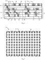
- the figures 4 and 5 are respectively a side sectional view and a top sectional view, partial and schematic, of an example of an electronic circuit suitable for hybrid molecular bonding.
- the electronic circuit 30 comprises an original electronic circuit 32, of which a base 34 has been shown, containing the substrate of the electronic circuit, electronic components, in particular transistors, and optionally the lower metallization levels of the electronic circuit 30, covered with upper interconnection levels 36, the original electronic circuit 32 being covered with a bonding interconnection level 40 for the realization of a hybrid molecular bonding.
- the interconnection levels 36 comprise a stack of insulating layers 42, four insulating layers 42 being represented by way of example in figure 4 , between and through which are provided conductive tracks 44 and conductive vias 46 connected to the electronic components, not shown, of the base 34.
- the bonding interconnection level 40 generally comprises a stack of a lower insulating layer 48 and an upper insulating layer 50.
- the upper insulating layer 50 delimits a planar bonding face 52.
- Conductive vias 54 called HBVs hereafter, extend through the lower insulating layer 48 and come into contact with tracks conductors 44.
- Conductive bonding pads 56 called HBM pads hereafter, are flush with the bonding face 52. Certain HBM pads 56 are electrically connected to HBVs 54, but other HBM pads 56 may not be electrically connected to HBVs 54.
- bonding interconnect level 40 may comprise a stack of more than two insulating layers.
- the figure 5 is a top sectional view in a plane parallel to the bonding face 52 and intersecting the HBM pads 56.
- the HBM pads 56 may have the same dimensions, in this example a square section in view On top.
- the cross section of each HBM 56 stud can be, in top view, inscribed in a square whose side is less than 10 ⁇ m, preferably less than 7 ⁇ m, more preferably less than 5 ⁇ m, even more preferably less than 3 ⁇ m , in particular less than 1 ⁇ m.
- the HBM pads 56 are separated by the insulating layer 50 by a minimum distance which depends in particular on the dimensions of the HBM pads 56, and which may be greater than 500 nm, preferably greater than 1 ⁇ m, more preferably greater than 3 ⁇ m, even more preferably greater than 5 ⁇ m.
- the HBM studs 56 can be distributed in a substantially homogeneous manner on the bonding face 52.
- Each HBM pad 56 can have a monolayer structure or a multilayer structure.
- the layer or each layer of the HBM pad 56 can be made of a metallic material used for the production of interconnection levels.
- the layer or each layer of the HBM pad 56 can be made of aluminum (Al), copper (Cu), copper and aluminum alloy, titanium (Ti), titanium nitride (TiN ), niobium (Nb), tungsten (W), or cobalt (Co) .
- each HBM pad 56 can be formed on a layer or a stack of layers acting as a grip for the formation of the HBM pad 56 and/or as a barrier for the diffusion of the material making up the HBM pad 56.
- the tie layer can be made of titanium (Ti) or of titanium nitride (TiN).
- the tie layer may have a thickness varying from 50 nm to 150 nm, for example equal to around 70 nm.
- the thickness of each HBM pad 56 is between 500 nm and 1.5 ⁇ m, for example equal to approximately 975 nm.
- Each insulating layer 48 and 50 can have a monolayer structure or a multilayer structure.
- the single layer forming the insulating layer 48, 50 or each layer of the insulating layer 48, 50 is made of silicon oxide (SiO 2 ), silicon nitride (SiN), silane, or orthosilicate tetraethyl (TEOS).
- the total thickness of the insulating layer 48 or 50 is between 100 nm and 4 ⁇ m.
- the bonding face 52 can be defined by a CMP step.
- CMP uses an abrasive and corrosive chemical suspension (usually a colloid) in conjunction with a polishing pad held on a polishing head.
- the pad and the electronic circuit board are pressed against each other.
- the pad has a roughness generally of the order of 50 ⁇ m.
- the polishing head and the wafer are rotated along parallel and non-concentric axes, so that the pad rubs against the wafer and causes material to be removed by mechanical action.
- the abrasive and corrosive chemical suspension is projected by a nozzle onto the wafer causing a removal of material by chemical etching and by mechanical action.
- the local density of conductive material exposed on the bonding face 52 is generally chosen to be less than or equal to 30%, preferably between 20% and 30%, for example approximately equal to 25%.
- the test pad 14 described above, can be produced by one of the conductive tracks 44.
- the inventors have put demonstrated that surface defects at the level of the test pads of the electronic circuit can prevent the proper progress of the known processes for preparing the electronic circuit for hybrid molecular bonding.
- the inventors have demonstrated that the lower insulating layer 48 of the level bonding interconnect 40 which is deposited and which covers the test pad may not be thick enough to compensate for the irregularities of the surface relief of the original electronic circuit 32, in particular when a CMP is subsequently carried out, so that the asperity 26, previously described, of the test pad 14 can be exposed.
- test pad in the bonding interconnection level 40 the test pad being made simultaneously with the HBM pads 56.
- the figures 6 and 7 are views respectively analogous to figures 4 and 5 of an example of an electronic circuit 60 suitable for hybrid molecular bonding which comprises all the elements of the electronic circuit 30 represented on the figures 4 and 5 with the difference that it further comprises at least one test pad 62, generally several test pads, formed in the same level as the HBM pads 56.
- the test pad 62 has the same composition as that of the HMB pads 56 previously described.
- test pad 62 is generally dictated by the tools used to perform the test.
- the test pad must have, in top view, a cross section in which is inscribed a square whose side dimension is greater than 30 ⁇ m, of preferably greater than 40 ⁇ m, for example equal to about 70 ⁇ m. This may not be compatible with obtaining by CMP a suitable surface state for the bonding face 52.
- a CMP process always leads to an overetching (in English “dishing”) of the HBM pads 56 with respect to the dielectric layer 50 which surrounds them. This overetching increases with the dimensions of the HBM 56 pad.
- contacting is followed by a thermal annealing step. This leads to an expansion of the HBM pads greater than the expansion of the dielectric regions and a contacting of the HBM pads of the two electronic circuits which remain glued at the end of the annealing.
- the cross section of an HBM pad in top view generally remains less than a square of 10 ⁇ m side so that the overetching is not too deep and remains compatible with the annealing step which follows the hybrid bonding.
- the overetching obtained after the CMP step delimiting the contact face 52 is too great so that, after the thermal annealing step, a local bonding defect between the two electronic circuits may be observed at test pad 62.
- test tips on the test pad 62 can lead to the deformation of the surface of the test pad 62 and in particular the formation of asperities on the surface of the test pad 62 which can be significant as has been previously described in relation to the picture 3 , so that a subsequent CMP does not make it possible to obtain the bonding face 52 with a suitable surface state for carrying out hybrid molecular bonding.
- FIGS. 8 and 9 are views respectively analogous to figures 6 and 7 of an embodiment of an electronic circuit 70 suitable for hybrid molecular bonding which comprises all the elements of the electronic circuit 60 represented on the figures 6 and 7 with the difference that each test pad 62 is replaced by a test pad 72, a single test pad being represented on the figures 8 and 9 .
- Each test pad 72 corresponds to a structure for which the density of conductive material flush with the bonding face 52 is greater than 40%, preferably between 40% and 80%, more preferably between 50% and 70%.
- the density of conductive material exposed on the bonding face 52 outside each test pad 72 is less than 35%, preferably less than 30%, more preferably less than 25%.
- the test stud 72 is inscribed in top view in a square whose side is between 30 ⁇ m and 100 ⁇ m.
- Test pad 72 has the same composition as HMB pads 56 described above.
- the test pad 72 has a structure such that, at any point of the test pad 72 exposed on the bonding face 52, a dimension of the test pad passing through this point is less than 10 ⁇ m, preferably less than 5 ⁇ m.
- the test pad 72 comprises a conductive layer 74 crossed by openings 76 containing the insulating material of the insulating layer 50.
- Each opening 76 can have, in top view, a cross section inscribed in a square whose side is between 2 ⁇ m and 7 ⁇ m, for example equal to approximately 5 ⁇ m.
- the minimum distance between two adjacent openings 76 can be greater than 2 ⁇ m, preferably greater than 5 ⁇ m.
- the figure 10 is a figure analogous to figure 9 representing a variant of the electronic circuit 70 in which the test pad 72 corresponds to a set of conductive pads 78 separated from each other by the insulating layer 50.
- the pads 78 can have the same dimensions as the HBM pads 56, the local density of the pads 78 being greater than the local density of the HBM pads 56.
- the majority of the pads 78 are connected to the conductive tracks 44 by HBVs 54.
- each pad 78 is connected to one of the conductive tracks 44 by an HBV 54 .
- test pad 72 can have the structure described previously in relation to the figure 9 , that is to say comprise a conductive layer 72 traversed by openings 76 containing an insulating material, and at least one other part of the test pad may have the structure described above in relation to the figure 10 , that is to say comprise a dense set of conductive pads 78 laterally separated by the upper insulating layer 50.
- the figure 11 represents, by a block diagram, an embodiment of a method of manufacturing an electronic system comprising a first electronic circuit 70, as described previously, fixed to a second electronic circuit by molecular hybrid bonding.
- the method comprises, for each of the electronic circuits, the formation of the level bonding interconnect 40 of electronic circuit 70 comprising at least one test pad 72.
- the method continues at step 82.
- HBM pads 56, HBVs 54, and test pads 72 can be formed according to a process manufacturing process in which the HBVs 54 and the HBM pads 56 are made by separate steps of depositing a conductive material, for example by a process of the simple damascene type.
- the HBVs 54 and the HBM pads 56 can be formed in a single step of depositing a conductive material, for example by a process of the double damascene type.
- the method comprises carrying out tests of the correct operation of the electronic circuit 70 by using the test pads 72 formed at step 80.
- the test can comprise bringing each test pad into contact 72 with a tip.
- the method continues at step 84.
- a planarization of the bonding face 52 is carried out. This can be achieved by CMP. This step makes it possible to obtain a bonding face 52 with a surface state suitable for carrying out hybrid molecular bonding.
- the method continues at step 86.
- the inventors have demonstrated that, with the structure of the test pads described previously, a bonding face 52 with a surface condition suitable for the production of hybrid molecular bonding can be obtained by CMP even when a test was performed.
- the maximum difference between the hollows and the peaks present on the bonding face 52 is less than 50 nm, preferably less than 20 nm.
- hybrid molecular bonding is achieved by bringing the bonding faces 52 of the two electronic circuits 70.
- the contacting step can be followed by thermal annealing.
- Tests have been carried out.
- two first electronic circuit boards were manufactured with test pads 62 each having the structure according to the figures 6 and 7 .
- a measurement of a profile curve of the bonding face 52 of one of the first plates was carried out.
- a molecular hybrid bonding was made between the first two electronic circuit boards.
- An image of the bonding faces bonded to each other was determined by ultrasound analysis on the electronic system obtained after hybrid molecular bonding, the bonding defects appearing in the form of lighter pixels on the image.
- test pads 72 were fabricated with test pads 72 each having the structure according to the figures 8 and 9 .
- a measurement of the profile curve of the bonding face of one of the second plates was carried out. There was no test step.
- a molecular hybrid bonding was made between the two second electronic circuit boards. An image of the bonding faces bonded to each other was determined by analysis by scanning acoustic microscopy on the electronic system obtained after hybrid molecular bonding.
- the figure 12 represents, in the central part, a profile curve P, expressed as a percentage, of the bonding face of an electronic circuit and, in the lower part, a partial image of the bonding face illustrating possible bonding defects for, in left part, a row R1 of test pads 62 of the first plate, and, in the right part, a row R2 of test pads 72 of the second plate.
- the profile curve is not compatible with hybrid molecular bonding, which results in bonding defects (white pixels D).
- the profile curve obtained is compatible with hybrid molecular bonding, which results in an absence of bonding defects.
- the third test is identical to the first test except that a test step followed by a CMP planarization step were implemented before the hybrid molecular bonding.
- the fourth test is identical to the second test except that a test step followed by a CMP planarization step were implemented before the hybrid molecular bonding.
- the figure 13 represents an image determined by analysis by acoustic microscopy of the bonding face 52 of the electronic circuit boards of the third test in the left part and of the fourth test in the right part.
Landscapes
- Internal Circuitry In Semiconductor Integrated Circuit Devices (AREA)
- Parts Printed On Printed Circuit Boards (AREA)
- Engineering & Computer Science (AREA)
- Manufacturing & Machinery (AREA)
- Non-Metallic Protective Coatings For Printed Circuits (AREA)
- Testing Or Measuring Of Semiconductors Or The Like (AREA)
Applications Claiming Priority (1)
| Application Number | Priority Date | Filing Date | Title |
|---|---|---|---|
| FR2011734A FR3116268B1 (fr) | 2020-11-16 | 2020-11-16 | Circuit électronique pour un collage moléculaire hybride |
Publications (2)
| Publication Number | Publication Date |
|---|---|
| EP4002441A2 true EP4002441A2 (de) | 2022-05-25 |
| EP4002441A3 EP4002441A3 (de) | 2023-01-04 |
Family
ID=74206027
Family Applications (1)
| Application Number | Title | Priority Date | Filing Date |
|---|---|---|---|
| EP21204895.3A Pending EP4002441A3 (de) | 2020-11-16 | 2021-10-27 | Elektronischer schaltkreis für eine hybride molekülverbindung |
Country Status (3)
| Country | Link |
|---|---|
| US (1) | US11990436B2 (de) |
| EP (1) | EP4002441A3 (de) |
| FR (1) | FR3116268B1 (de) |
Families Citing this family (9)
| Publication number | Priority date | Publication date | Assignee | Title |
|---|---|---|---|---|
| TWI822659B (zh) | 2016-10-27 | 2023-11-21 | 美商艾德亞半導體科技有限責任公司 | 用於低溫接合的結構和方法 |
| US10515913B2 (en) | 2017-03-17 | 2019-12-24 | Invensas Bonding Technologies, Inc. | Multi-metal contact structure |
| US10446441B2 (en) | 2017-06-05 | 2019-10-15 | Invensas Corporation | Flat metal features for microelectronics applications |
| US11244916B2 (en) | 2018-04-11 | 2022-02-08 | Invensas Bonding Technologies, Inc. | Low temperature bonded structures |
| US11244920B2 (en) | 2018-12-18 | 2022-02-08 | Invensas Bonding Technologies, Inc. | Method and structures for low temperature device bonding |
| CN116848631A (zh) | 2020-12-30 | 2023-10-03 | 美商艾德亚半导体接合科技有限公司 | 具有导电特征的结构及其形成方法 |
| JP2023034974A (ja) * | 2021-08-31 | 2023-03-13 | キオクシア株式会社 | 半導体装置および基板 |
| US12545010B2 (en) | 2022-12-29 | 2026-02-10 | Adeia Semiconductor Bonding Technologies Inc. | Directly bonded metal structures having oxide layers therein |
| US12506114B2 (en) | 2022-12-29 | 2025-12-23 | Adeia Semiconductor Bonding Technologies Inc. | Directly bonded metal structures having aluminum features and methods of preparing same |
Family Cites Families (6)
| Publication number | Priority date | Publication date | Assignee | Title |
|---|---|---|---|---|
| US10515913B2 (en) * | 2017-03-17 | 2019-12-24 | Invensas Bonding Technologies, Inc. | Multi-metal contact structure |
| US10840205B2 (en) * | 2017-09-24 | 2020-11-17 | Invensas Bonding Technologies, Inc. | Chemical mechanical polishing for hybrid bonding |
| KR102674029B1 (ko) * | 2018-10-26 | 2024-06-13 | 삼성전자주식회사 | 테스트 패드를 포함하는 반도체 패키지 |
| FR3095719A1 (fr) * | 2019-05-03 | 2020-11-06 | Commissariat A L'energie Atomique Et Aux Energies Alternatives | Procédé de collage moléculaire hybride et circuit électronique pour la mise en oeuvre d'un tel procédé |
| US11862602B2 (en) * | 2019-11-07 | 2024-01-02 | Adeia Semiconductor Technologies Llc | Scalable architecture for reduced cycles across SOC |
| US11527500B2 (en) * | 2020-03-20 | 2022-12-13 | Sandisk Technologies Llc | Semiconductor structure containing multilayer bonding pads and methods of forming the same |
-
2020
- 2020-11-16 FR FR2011734A patent/FR3116268B1/fr active Active
-
2021
- 2021-10-27 EP EP21204895.3A patent/EP4002441A3/de active Pending
- 2021-11-05 US US17/519,957 patent/US11990436B2/en active Active
Also Published As
| Publication number | Publication date |
|---|---|
| FR3116268A1 (fr) | 2022-05-20 |
| US11990436B2 (en) | 2024-05-21 |
| EP4002441A3 (de) | 2023-01-04 |
| US20220157752A1 (en) | 2022-05-19 |
| FR3116268B1 (fr) | 2023-10-20 |
Similar Documents
| Publication | Publication Date | Title |
|---|---|---|
| EP4002441A2 (de) | Elektronischer schaltkreis für eine hybride molekülverbindung | |
| EP2192612B1 (de) | Verfahren zum Stapeln und Vernetzen von integrierten Schaltkreisen | |
| EP2054929B1 (de) | Prozess zur kollektiven herstellung von elektronischen 3d-modulen | |
| EP1365444B1 (de) | Grabenkondensator mit zwei vom Substrat unabhängigen Elektroden | |
| FR3021455A1 (fr) | Procede d'aplanissement d'evidements remplis de cuivre | |
| EP3261116B1 (de) | Verfahren zur gemeinsamen herstellung von elektronischen 3d-modulen | |
| EP3913657A2 (de) | Verfahren zur verarbeitung einer elektronischen schaltung für hybride molekulare klebung | |
| FR2990297A1 (fr) | Empilement de structures semi-conductrices et procede de fabrication correspondant | |
| EP1111669A1 (de) | Verfahren zur Herstellung von isolierten metallischen Verbindungsleitungen in integrierten Schaltkreisen | |
| EP3742478B1 (de) | Selbstassemblierungsverfahren mit hybrider molekülverbindung | |
| FR3095719A1 (fr) | Procédé de collage moléculaire hybride et circuit électronique pour la mise en oeuvre d'un tel procédé | |
| EP4222783A1 (de) | Optoelektronische vorrichtung | |
| FR3093592A1 (fr) | Circuit intégré comportant un condensateur tridimensionnel | |
| EP4152373A2 (de) | Verfahren zur herstellung eines elektronischen schaltkreises für die selbstmontage an einem anderen elektronischen schaltkreis | |
| EP1180790B1 (de) | Kondensatorherstellung mit metallischen Elektroden | |
| FR3103315A1 (fr) | Procédé de fabrication de puces électroniques | |
| EP3832707A1 (de) | Verbindungsstruktur eines phasenwechselspeichers | |
| EP4505511B1 (de) | Substrat mit vias und zugehörige herstellungsverfahren | |
| FR2901635A1 (fr) | Dispositif de connexion tridimensionnel dans un substrat | |
| EP4528806B1 (de) | Elektronischer chip mit anschlusssäulen | |
| FR3091410A1 (fr) | Procédé de gravure | |
| FR3076658A1 (fr) | Procede de gravure d'une cavite dans un empilement de couches | |
| WO2022229830A1 (fr) | Procédé de réalisation d'une structure d'interconnexion à plots entre microcircuits | |
| FR3143841A1 (fr) | Procédé de préparation d’un empilement en vue d’un collage | |
| EP4120332A1 (de) | Verfahren zur herstellung von elektronischen chips |
Legal Events
| Date | Code | Title | Description |
|---|---|---|---|
| PUAI | Public reference made under article 153(3) epc to a published international application that has entered the european phase |
Free format text: ORIGINAL CODE: 0009012 |
|
| STAA | Information on the status of an ep patent application or granted ep patent |
Free format text: STATUS: REQUEST FOR EXAMINATION WAS MADE |
|
| 17P | Request for examination filed |
Effective date: 20211027 |
|
| AK | Designated contracting states |
Kind code of ref document: A2 Designated state(s): AL AT BE BG CH CY CZ DE DK EE ES FI FR GB GR HR HU IE IS IT LI LT LU LV MC MK MT NL NO PL PT RO RS SE SI SK SM TR |
|
| REG | Reference to a national code |
Ref country code: DE Ref legal event code: R079 Free format text: PREVIOUS MAIN CLASS: H01L0023000000 Ipc: H01L0023485000 |
|
| PUAL | Search report despatched |
Free format text: ORIGINAL CODE: 0009013 |
|
| AK | Designated contracting states |
Kind code of ref document: A3 Designated state(s): AL AT BE BG CH CY CZ DE DK EE ES FI FR GB GR HR HU IE IS IT LI LT LU LV MC MK MT NL NO PL PT RO RS SE SI SK SM TR |
|
| RIC1 | Information provided on ipc code assigned before grant |
Ipc: H01L 21/66 20060101ALN20221201BHEP Ipc: H01L 23/485 20060101AFI20221201BHEP |
|
| RAP3 | Party data changed (applicant data changed or rights of an application transferred) |
Owner name: COMMISSARIAT A L'ENERGIE ATOMIQUE ET AUX ENERGIESALTERNATIVES |