EP4002453B1 - Structure de sortie de ligne de mots et son procédé de préparation - Google Patents
Structure de sortie de ligne de mots et son procédé de préparation Download PDFInfo
- Publication number
- EP4002453B1 EP4002453B1 EP21812445.1A EP21812445A EP4002453B1 EP 4002453 B1 EP4002453 B1 EP 4002453B1 EP 21812445 A EP21812445 A EP 21812445A EP 4002453 B1 EP4002453 B1 EP 4002453B1
- Authority
- EP
- European Patent Office
- Prior art keywords
- word line
- contact hole
- layer
- metal
- axis direction
- Prior art date
- Legal status (The legal status is an assumption and is not a legal conclusion. Google has not performed a legal analysis and makes no representation as to the accuracy of the status listed.)
- Active
Links
Images


Classifications
-
- H—ELECTRICITY
- H10—SEMICONDUCTOR DEVICES; ELECTRIC SOLID-STATE DEVICES NOT OTHERWISE PROVIDED FOR
- H10B—ELECTRONIC MEMORY DEVICES
- H10B12/00—Dynamic random access memory [DRAM] devices
- H10B12/30—DRAM devices comprising one-transistor - one-capacitor [1T-1C] memory cells
- H10B12/48—Data lines or contacts therefor
- H10B12/488—Word lines
-
- G—PHYSICS
- G11—INFORMATION STORAGE
- G11C—STATIC STORES
- G11C5/00—Details of stores covered by group G11C11/00
- G11C5/06—Arrangements for interconnecting storage elements electrically, e.g. by wiring
- G11C5/063—Voltage and signal distribution in integrated semi-conductor memory access lines, e.g. word-line, bit-line, cross-over resistance, propagation delay
-
- G—PHYSICS
- G11—INFORMATION STORAGE
- G11C—STATIC STORES
- G11C5/00—Details of stores covered by group G11C11/00
- G11C5/02—Disposition of storage elements, e.g. in the form of a matrix array
- G11C5/025—Geometric lay-out considerations of storage- and peripheral-blocks in a semiconductor storage device
-
- H—ELECTRICITY
- H10—SEMICONDUCTOR DEVICES; ELECTRIC SOLID-STATE DEVICES NOT OTHERWISE PROVIDED FOR
- H10D—INORGANIC ELECTRIC SEMICONDUCTOR DEVICES
- H10D84/00—Integrated devices formed in or on semiconductor substrates that comprise only semiconducting layers, e.g. on Si wafers or on GaAs-on-Si wafers
- H10D84/80—Integrated devices formed in or on semiconductor substrates that comprise only semiconducting layers, e.g. on Si wafers or on GaAs-on-Si wafers characterised by the integration of at least one component covered by groups H10D12/00 or H10D30/00, e.g. integration of IGFETs
-
- H—ELECTRICITY
- H10—SEMICONDUCTOR DEVICES; ELECTRIC SOLID-STATE DEVICES NOT OTHERWISE PROVIDED FOR
- H10W—GENERIC PACKAGES, INTERCONNECTIONS, CONNECTORS OR OTHER CONSTRUCTIONAL DETAILS OF DEVICES COVERED BY CLASS H10
- H10W20/00—Interconnections in chips, wafers or substrates
- H10W20/01—Manufacture or treatment
- H10W20/031—Manufacture or treatment of conductive parts of the interconnections
-
- H—ELECTRICITY
- H10—SEMICONDUCTOR DEVICES; ELECTRIC SOLID-STATE DEVICES NOT OTHERWISE PROVIDED FOR
- H10W—GENERIC PACKAGES, INTERCONNECTIONS, CONNECTORS OR OTHER CONSTRUCTIONAL DETAILS OF DEVICES COVERED BY CLASS H10
- H10W20/00—Interconnections in chips, wafers or substrates
- H10W20/40—Interconnections external to wafers or substrates, e.g. back-end-of-line [BEOL] metallisations or vias connecting to gate electrodes
- H10W20/41—Interconnections external to wafers or substrates, e.g. back-end-of-line [BEOL] metallisations or vias connecting to gate electrodes characterised by their conductive parts
- H10W20/43—Layouts of interconnections
-
- H—ELECTRICITY
- H10—SEMICONDUCTOR DEVICES; ELECTRIC SOLID-STATE DEVICES NOT OTHERWISE PROVIDED FOR
- H10B—ELECTRONIC MEMORY DEVICES
- H10B12/00—Dynamic random access memory [DRAM] devices
- H10B12/01—Manufacture or treatment
- H10B12/02—Manufacture or treatment for one transistor one-capacitor [1T-1C] memory cells
- H10B12/05—Making the transistor
- H10B12/053—Making the transistor the transistor being at least partially in a trench in the substrate
-
- H—ELECTRICITY
- H10—SEMICONDUCTOR DEVICES; ELECTRIC SOLID-STATE DEVICES NOT OTHERWISE PROVIDED FOR
- H10D—INORGANIC ELECTRIC SEMICONDUCTOR DEVICES
- H10D89/00—Aspects of integrated devices not covered by groups H10D84/00 - H10D88/00
- H10D89/10—Integrated device layouts
Definitions
- the disclosure relates to the field of a semiconductor, and specifically to a word line lead-out structure and a method for preparing of a bit word lead-out structure.
- a semiconductor memory uses a transistor array to control the charging and discharging of a storage capacitor to realize data access.
- a gate of the transistor is electrically connected with a word line. After the word line is formed in a substrate, a word line lead-out structure needs to be formed above the word line to reach an electric connection between the word line and an external control circuit.
- the size of a word line and the space between word lines are increasingly reduced; correspondingly, the area of the word line lead-out structure is increasingly reduced.
- the contact resistance between the word line lead-out structure and corresponding words line is increased, so that a current flowing through the word line is reduced, thereby reducing and the induction margin of the semiconductor device and the charging and discharging speed of the storage capacitor.
- US 2015/228658 A1 describes the layout of a semiconductor device where embedded word line is connected to a metal wiring line by means of a contact. Background may be found in CN110021599A (SAMSUNG ELECTRONICS CO., LTD.) 16 July 2019 & US 2019/206877 A1 (KIM DONG-WAN [KR] ET AL) 4 July 2019 .
- first, second, third, and the like may be used to describe various elements, components, regions, layers, doping types and/or parts, these elements, components, regions, layers, doping types and/or parts should not be limited by these terms. These terms are only used to distinguish one element, component, region, layer, doping type, or part from another element, component, region, layer, doping type, or part. Therefore, a first element, component, region, layer, doping type, or part discussed below may be represented as a second element, component, region, layer or part without departing from the teaching of the disclosure.
- Spatial relation terms such as “under”, “underneath”, “lower”, “below”, “above”, “upper”, and the like, may be used herein to describe a relation between one element or feature and another element or feature as illustrated in the figures. It is to be understood that in addition to the orientation shown in the figures, the spatial relation terms further include different orientations of a device in use and operation. For example, if the device in the figures is turned over, the element or feature described as “underneath the other element” or “below it” or “under it”, the element or feature will be oriented “over” the other element or feature. Therefore, the exemplary terms “underneath” and “below” may include both above and below. In addition, the device may also include additional orientations (for example, rotated 90 degrees or other orientations), and the spatial descriptors used herein are interpreted accordingly.
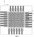
- FIG. 1 is a top view of a word line lead-out structure in one embodiment of the present application.
- FIG. 2 is a side cross-sectional view corresponding to a section line AA' in FIG. 1 .
- the word line lead-out structure includes a word line 120, a contact hole 310, and a metal line 410.
- the word line 120 extends along an X-axis direction.
- the contact hole 310 is located above the word line 120 and covers the word line 120 along a Y-axis direction, and the Y-axis direction is perpendicular to the X-axis direction.
- the contact hole 310 covering the word line 120 along the Y-axis direction means that a width of the contact hole 310 along the Y-axis direction is greater than or equal to that of the word line 120 along the Y-axis direction, and the contact hole 310 covers a segment of the word line 120 along the X-axis direction.
- the metal line 410 is located on the contact hole 310 and covers the contact hole 310, that is, the contact hole 310 is located between the word line 120 and the metal line 410, a bottom surface of the contact hole 310 is in contact with the word line 120, and a top surface of the contact hole 310 is in contact with the metal line 410.
- the contact area between the contact hole 310 and the metal line 410 is larger than that between the contact hole 310 and the word line 120, and the width of the contact surface between the contact hole 310 and the metal line 410 along the Y-axis direction is greater than the width of the contact surface between the contact hole 310 and the word line 120 along the Y-axis direction.
- the word line 120 is formed in a semiconductor device.
- the contact hole 310 and the metal line 410 above the word line 120, an external electric signal is transmitted to the word line 120 through the metal line 410 and the contact hole 310, and the semiconductor device is controlled through the word line 120.
- the contact hole 310 covers the word line 120 along the Y-axis direction
- the metal line 410 covers the contact hole 310.
- the contact area between the contact hole 310 and the metal line 410 is larger than that between the contact hole 310 and the word line 120.
- the contact area between the contact hole 310 and the word line 120 is relatively small, so that the influence of the contact hole 310 on the integration level of the device is reduced.
- the contact area between the contact hole 310 and the metal line 410 is relatively large, so that the contact resistance of the whole word line lead-out structure is reduced, thereby improving the induction margin of the semiconductor memory and the charging and discharging speed of a storage capacitor.
- a cross-section of the contact hole 310 is a T-shaped structure, that is, a section of the contact hole 310 along a Z-axis direction shown in FIG. 2 is the T-shaped structure.
- the X-axis, the Y-axis, and the Z-axis are perpendicular to each other.
- the contact hole 310 is the T-shaped structure, and the width of the top surface of the contact hole 310 along the Y-axis direction is greater than the width of the bottom surface the contact hole 310 along the Y-axis direction, so that the contact area between the contact hole 310 and the metal line 410 is larger than that between the contact hole 310 and the word line 120.
- a substrate 100 is provided with a first groove 101 extending along the X-axis direction, the word line 120 is filled in the first groove 101, and the thickness of the word line 120 is smaller than the depth of the first groove 101, that is, the top surface of the word line 120 is lower than the top surface of the substrate 100.
- a part of the contact hole 310 is filled in the first groove 101, the contact hole 310 located outside the first groove 101 extends to the substrate 100 at both sides of the word line 120 along the Y-axis direction. At this time, the contact hole 310 located in the first groove 101 together with the contact hole 310 located outside the first groove 101 together form the contact hole 310 with the T-shaped structure.
- the width of the metal line 410 above the contact hole 310 along the Y-axis direction is equal to that of the contact hole 310 along the Y-axis direction, and side surfaces of the contact hole 310 and the metal line 410 extending along the X-axis direction are aligned with each other.
- the word line 120 includes a metal structure 121 located at the bottom of the first groove 101, and a polysilicon structure located at the top of the metal structure 121.
- the polysilicon structure of the word line in a region covered by the contact hole 310 is removed, that is, the word line in the region covered by the contact hole 310 does not include the polysilicon structure, and the contact hole 310 is in direct contact with the metal structure 121, thereby reducing parasitic resistance between the word lines.
- the word line lead-out structure includes 2 * N word lines 120, each of the word line 120 is distributed in parallel along the Y-axis direction, 2 * N contact holes 310 are respectively formed on the 2 * N word lines 120, 2 * N metal lines 410 are respectively formed on the 2 * N contact holes 310, and each of the metal line 410 extends along the X-axis direction.
- N is a positive integer
- the 2 * N word lines 120, the 2 * N contact holes 310 and the 2 * N metal lines 410 are in one-to-one correspondence.
- the 2 * N word lines 120 which are distributed in parallel along the Y-axis direction are formed on the substrate 100.
- each word line 120 corresponds to one independent word line lead-out structure, so that each word line 120 is independently controlled.
- the 2 * N word lines 120 are aligned in the Y-axis direction, that is, the 2 * N word lines 120 are the same in length along the X-axis direction, and an endpoint of each of the word lines 120 is aligned along the Y-axis direction.
- N metal lines 410 and N contact holes 310 are located at one side of the word line 120 along the X-axis direction, and the other N metal lines 410 and the other N contact holes 310 are located at the other side of the word line 120 along the X-axis direction.
- the metal lines 410 at the same side are distributed in parallel along the Y-axis direction.
- 2 * N lead-out structures formed by the 2 * N contact holes 310 and the 2 * N metal lines 410 are divided into two groups of the lead-out structures.
- a first group of the lead-out structures include N contact holes 310, and N metal lines 410 in contact with the N contact holes 310.
- the contact hole 310 and the metal line 410 at one side of the word line 120 cover the odd-numbered word lines 120
- the contact hole 310 and the metal line 410 at the other side of the word line 120 cover the even-numbered word lines 120.
- the 2 * N word lines 120 are sequentially arranged along the Y-axis direction
- the first group of the lead-out structures are arranged on the odd-numbered word lines 120
- the second group of the lead-out structures are arranged on the even-numbered word lines 120, so that the space between adjacent contact holes 310 is increased, further, the width of the contact hole 310 and the metal line 410 is increased, the contact area is increased, and the contact resistance is reduced.
- the conductivity of the contact hole 310 is different from the conductivity of the metal line 410, that is, materials of the metal line 410 and the contact hole 310 are different.
- the material of the contact hole 310 may be metal or metal alloy including one or more of copper, aluminum, nickel, tungsten, silver, gold, and the like.
- the metal line 410 may be one of a copper line, an aluminum line, a nickel line, a tungsten line, a silver line, a gold line, and the like.
- FIG. 3 shows a method for preparing a word line lead-out structure in one embodiment of the present application.
- the method for preparing a word line lead-out structure includes the following operations.
- a first groove extending along an X-axis direction is formed in a substrate.
- a word line extending along the X-axis direction is formed in the first groove.
- a top surface of the word line is lower than that of the substrate.
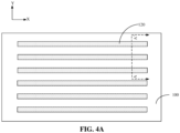
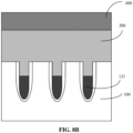
- FIG. 4A is a top view in which the word line 120 is formed
- FIG. 4B is a side cross-sectional view corresponding to a section line AA' in FIG. 4A .
- the first groove 101 extending along the X-axis direction is provided in the substrate 100
- the word line 120 extending along the X-axis direction is formed in the first groove 101.
- the top surface of the word line 120 is lower than the top surface of the substrate 100, that is, the thickness of the word line 120 is smaller than the depth of the first groove 101.
- the word line 120 includes a metal structure 121 at the bottom of the first groove 101 and a polysilicon structure 122 located on the metal structure 121.
- the substrate 100 is provided with 2 * N first grooves 101 respectively extending along the X-axis direction, and each of the grooves is distributed in parallel along the Y-axis direction.
- 2 * N word lines 120 extending along the X-axis direction are formed in the 2 * N first grooves 101, and each of the word lines 120 is distributed in parallel along the Y-axis direction.
- the above word lines 120 are aligned in the Y-axis direction, that is, the 2 * N word lines 120 are the same in length along the X-axis direction, and an endpoint of each of the word lines 120 is aligned along the Y-axis direction.
- a procedure of forming the word line 120 includes the following operations.
- a word line material layer is deposited in the first groove and on the substrate outside the first groove.
- one word line material layer is deposited through a deposition process.
- the word line material layer has certain thickness and covers the first groove 101 and the substrate 100.
- the top surface of the word line material layer is flattened; the word line material layer on the substrate is removed so that the word line material layer in the first groove is reserved.
- the word line material layer After the word line material layer is deposited, the word line material layer has an uneven upper surface. Next, the upper surface of the word line material layer is ground through a chemical mechanical grinding process, so that the upper surface of the word line material layer is flattened. The word line material layer is etched to expose the substrate 100, so that the word line material layer in the first groove 101 is reserved.
- the word line material layer in the first groove is etched back, the word line material layer at the top of the first groove is removed, so that the word line material layer at the bottom of the first groove is reserved, thereby forming the word line.
- the word line material layer in the first groove 101 is etched through an etching process to reduce the thickness of the word line material layer, so that the thickness of the word line material layer is smaller than the depth of the first groove 101. After etching is stopped, the reserved word line material layer forms the word line 120.
- the etch-back depth of the word line material layer can be flexibly selected according to specific requirements.
- a contact hole layer is formed on the word line and on the substrate outside the first groove.
- the contact hole layer 300 is formed directly on the word line 120 and on the substrate 100 outside the first groove 101.
- S300 includes the following sub-operations.
- a dielectric layer is formed on the substrate and the first groove.
- the dielectric layer 200 is deposited on the substrate 100 and the first groove 101 through the deposition process, and the top surface of the dielectric layer 200 is ground to flatten the top surface of the dielectric layer 200.
- the dielectric layer is etched to form a second groove extending along the Y-axis direction.
- the second groove penetrates through the dielectric layer and exposes the word line and the substrate.
- FIG. 5A is a top view in which a second groove 201 is formed in the dielectric layer 200
- FIG. 5B corresponds to a side cross-sectional view of a section line AA' in FIG. 5A
- the dielectric layer 200 is etched.
- the second groove 201 extending along the Y-axis direction is formed on the dielectric layer 200.
- the second groove 201 penetrates through the dielectric layer 200 along a Z-axis direction and exposes the word line 120 (specifically, the polysilicon structure 122 in the word line 120) and the substrate 100 at the bottom of the second groove 201.
- the etching selectivity ratio of the dielectric layer 200 and the substrate 100 is different, so that the substrate 100 is not substantially etched during the etching of the dielectric layer 200 to form the second groove 201.
- two second grooves 201 respectively extending along the Y-axis direction are formed in the dielectric layer 200.
- One of the second grooves 201 is located at one side of the word line 120 extending along the X-axis direction, and the other of the second grooves 201 is located at the other side of the word line 120 extending along the X-axis direction, that is, the two second grooves 201 are distributed in parallel along the X-axis direction.
- the two second grooves 201 are respectively close to end points on two sides of the word line 120 along the X-axis direction.
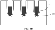
- FIG. 6A is a top view in which an exposed polysilicon structure is removed
- FIG. 6B corresponds to a side cross-sectional view of a section line AA' in FIG. 6A .
- the contact hole layer is formed in the first groove and the second groove.
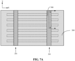
- FIG. 7A is a top view in which the first groove 101 and the second groove 201 are filled with the contact hole layer 300
- FIG. 7B corresponds to a side cross-sectional view of a section line AA' in FIG. 7A
- a thicker layer of contact hole material is deposited through a deposition process, the contact hole material fills the exposed first groove 101 and second groove 201 and is higher than the dielectric layer 200, then the contact hole material is flattened through a grinding process, the contact hole material above the dielectric layer 200 is removed, so that only the contact hole material in the first groove 101 and the second groove 201 is reserved, thereby forming the required contact hole layer 300.
- the contact hole layer 300 is formed through S311 to S313. In other embodiments, the required contact hole layer 300 can also be formed through the following sub-operations S321 to S323.
- the contact hole material is deposited on the substrate 100 and the first groove 101.
- the contact hole material is etched, so that the contact hole material at two sides is removed to form the contact hole layer 300 extending along the Y-axis direction.
- a dielectric material is deposited and flattened. The dielectric material layer above the contact hole layer 300 is removed, the contact hole layer 300 is exposed, and the dielectric material at two sides of the contact hole layer 300 is reserved to form the dielectric layer 200.
- a metal layer is formed on the contact hole layer.
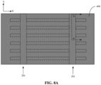
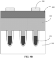
- FIG. 8A is a top view in which a metal layer 400 is formed
- FIG. 8B is a side cross-sectional view corresponding to a section line AA' in FIG. 8A
- the metal layer 400 is formed on the contact hole layer 300 through the deposition process.
- the contact hole layer 300 is formed in the second groove 201
- the metal layer 400 is formed on the contact hole layer 300 and the dielectric layer 200.
- the metal layer and the contact hole layer are etched to form the word line lead-out structure.
- the metal layer 400 and the contact hole layer 300 are etched.
- the metal layer 400 is etched to form the metal line 410
- the contact hole layer 300 is etched to form the contact hole 310, so that the word line lead-out structure is formed.
- a location relation of the word line 120, the contact hole 310 and the metal line 410 in the word line lead-out structure has been described above and will not be described in detail herein.
- the operation that the metal layer 400 and the contact hole layer 300 are etched specifically includes that: a mask is formed on the metal layer 400, the exposed metal layer 400 is etched downward under the protection of the mask to form the metal line 410, and the exposed contact hole layer 300 is continuously etched downward under the protection of the metal line 410 to form the contact hole 310. That is, the above etching of the contact hole layer 300 belongs to self-aligned etching, and boundaries of the contact hole 310 and the metal line 410 formed after the self-aligned etching are aligned, so that an influence on the electric performance of a device resulted from an offset between the contact hole layer 310 and the metal line 410 is prevented.
- S500 includes the following operations.
- each of the masks spans the second groove 201 along the X-axis direction and covers a word line along the Y-axis direction.
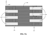
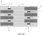
- FIG. 9A is a top view in which 2 * N masks 500 are formed
- FIG. 8B corresponds to a side cross-sectional view of a section line AA' in FIG. 8A
- the 2 * N masks 500 are formed on the metal layer 400, each of the masks 500 spans the second groove 201 along the X-axis direction and one mask 500 covers one word line 120 along the Y-axis direction, that is, the 2 * N masks 500 and the 2 * N word lines 120 are in one-to-one correspondence.
- two second grooves 201 are formed in the dielectric layer 200, when two contact hole layers 300 extending along the Y-axis direction are respectively correspondingly formed in the two second grooves 201, among the 2 * N masks 500, N masks 500 are located at one side of the metal layer 400 along the X-axis direction and span the second grooves 201 located at the same side along the X-axis direction, and respectively cover the odd-numbered word lines 120.
- the other N masks 500 are located at the other side of the metal layer 400 along the X-axis direction and span the other second grooves 201 located at the same side along the X-axis direction, and respectively cover the even-numbered word lines. Further, the masks 500 at the same side are distributed in parallel along the Y-axis direction.
- the metal layer and the contact hole layer are sequentially etched, the metal layer below the mask is reserved to form 2 * N metal lines, and the contact hole layer below the metal line is reserved to form 2 * N contact holes.
- N is a positive integer, and the 2 * N word lines, the 2 * N contact holes and the 2 * N metal lines are in one-to-one correspondence.
- FIG. 10A is a top view in which the 2 * N metal lines 410 are formed
- FIG. 10B corresponds to a side cross-sectional view of a section line AA' in FIG. 10A
- the exposed metal layer 400 is etched under the protection of the 2 * N masks to form the 2 * N independent metal lines 410
- the exposed contact hole layer 300 is continuously etched under the protection of the metal lines 410 to form the 2 * N independent contact holes 310.
- the 2 * N word lines 120, the 2 * N contact holes 310 and the 2 * N metal lines 410 are in one-to-one correspondence.
- Each of the word lines 120 is led out through the contact hole 310 and the metal line 410 above the word line 120.
- the contact hole layer 300 extending along the Y-axis direction is formed first, the contact hole layer 300 is integrally formed and electrically connected with multiple word lines 120, then the metal layer 400 is formed on the contact hole layer 300 and on the dielectric layer 200, the mask 600 is formed on the metal layer 400, the mask 600 spans the second groove 201 along the X-axis direction. Next, the exposed metal layer 400 and contact hole layer 300 are sequentially etched under a shielding effect of the mask 600, the contact hole layer 300 extending along the Y-axis direction is cut into multiple independent parts. The metal layer 400 and contact hole layer 300 that are not etched form a lead-out structure of the word line 120.
- the self-aligned etching is used for the contact hole layer 300 as described above, an alignment step of front and back etching in a conventional technology is omitted.
- the boundaries of the reserved metal layer 400 and the reserved contact hole layer 300 after etching are flush, the metal layer 400 and the contact hole layer 300 do not have location offset, thereby greatly improving the electric performance of a semiconductor device.
- the above-described word line lead-out structure is formed by the above preparation method of a word line lead-out structure.
- the contact hole 310 covers the word line 120 along the Y-axis direction
- the metal line 410 covers the contact hole 310
- the contact area between the contact hole 310 and the metal line 410 is larger than the contact area between the contact hole 310 and the word line 120.
- the contact area between the contact hole 310 and the word line 120 is relatively small, so that the influence of the contact hole 310 on the integration level of the device is reduced.
- the contact area between the contact hole 310 and the metal line 410 is relatively large, so that the contact resistance of the whole word line lead-out structure is reduced, thereby improving the induction margin of the semiconductor memory and the charging and discharging speed of a storage capacitor.
Landscapes
- Engineering & Computer Science (AREA)
- Microelectronics & Electronic Packaging (AREA)
- Internal Circuitry In Semiconductor Integrated Circuit Devices (AREA)
- Semiconductor Memories (AREA)
Claims (3)
- Procédé de préparation d'une structure de sortie de ligne de mots, comprenant :la réalisation d'une première rainure (101) dans un substrat (100) ;la formation de la ligne de mots (120) s'étendant le long de la direction de l'axe X dans la première rainure (101), une surface supérieure de la ligne de mots (120) étant inférieure à une surface supérieure du substrat (100) ;la formation de la couche de trous de contact (300) sur la ligne de mots (120) et le substrat (100) ;la formation de la couche métallique (400) sur la couche de trous de contact (300) ; etla gravure de la couche métallique (400) et de la couche de trous de contact (300) pour former la structure de sortie de ligne de mots, dans lequel ladite formation de la couche de trous de contact (300) sur la ligne de mots (120) et le substrat (100) comprend :la formation d'une couche diélectrique (200) sur le substrat (100) et la ligne de mots (120),la gravure de la couche diélectrique (200) pour former une seconde rainure s'étendant le long de la direction de l'axe Y, la seconde rainure pénétrant à travers la couche diélectrique (200) et exposant la ligne de mots (120) et le substrat (100), etla formation de la couche de trous de contact (300) dans la première rainure (101) et la seconde rainure (201).
- Procédé selon la revendication 1, dans lequel 2 * N lignes de mots (120) sont formées dans le substrat (100), chacune des lignes de mots (120) étant répartie parallèlement le long de la direction de l'axe Y ;
ladite gravure de la couche métallique (400) et de la couche de trous de contact (300) comprend :la formation de 2 * N masques (500) sur la couche métallique (400), chacun des masques (500) recouvrant la seconde rainure (201) le long de la direction de l'axe X et couvrant une ligne de mots (120) le long de la direction de l'axe Y, etla gravure successive de la couche métallique (400) et de la couche de trous de contact (300), en réservant la couche métallique (400) sous le masque (500) pour former 2 * N lignes métalliques (410), en réservant la couche de trous de contact (300) sous la ligne métallique (410) pour former 2 * N trous de contact (310), dans lequel N est un nombre entier positif, et les 2 * N lignes de mots (120), les 2 * N trous de contact (310) et les 2 * N lignes métalliques (410) sont en correspondance biunivoque. - Procédé selon la revendication 2, dans lequel la ligne de mots (120) comprend la structure métallique (121) située en bas, et la structure de polysilicium (122) empilée sur la structure métallique (121), avant ladite formation de la couche de trous de contact (300) dans la seconde rainure (201), comprenant en outre : le retrait de la structure de polysilicium (122), et la mise en réserve de la structure métallique (121).
Applications Claiming Priority (2)
| Application Number | Priority Date | Filing Date | Title |
|---|---|---|---|
| CN202010468064.XA CN113745193B (zh) | 2020-05-28 | 2020-05-28 | 字线引出结构及其制备方法 |
| PCT/CN2021/094069 WO2021238696A1 (fr) | 2020-05-28 | 2021-05-17 | Structure de sortie de ligne de mots et son procédé de préparation |
Publications (3)
| Publication Number | Publication Date |
|---|---|
| EP4002453A1 EP4002453A1 (fr) | 2022-05-25 |
| EP4002453A4 EP4002453A4 (fr) | 2022-11-16 |
| EP4002453B1 true EP4002453B1 (fr) | 2025-03-26 |
Family
ID=78707027
Family Applications (1)
| Application Number | Title | Priority Date | Filing Date |
|---|---|---|---|
| EP21812445.1A Active EP4002453B1 (fr) | 2020-05-28 | 2021-05-17 | Structure de sortie de ligne de mots et son procédé de préparation |
Country Status (2)
| Country | Link |
|---|---|
| US (1) | US11862281B2 (fr) |
| EP (1) | EP4002453B1 (fr) |
Citations (1)
| Publication number | Priority date | Publication date | Assignee | Title |
|---|---|---|---|---|
| US20190206877A1 (en) * | 2018-01-03 | 2019-07-04 | Samsung Electronics Co., Ltd. | Semiconductor memory device |
Family Cites Families (12)
| Publication number | Priority date | Publication date | Assignee | Title |
|---|---|---|---|---|
| JPS6030170A (ja) * | 1983-07-29 | 1985-02-15 | Hitachi Ltd | 高集積読み出し専用メモリ |
| JP4635333B2 (ja) | 2000-12-14 | 2011-02-23 | ソニー株式会社 | 半導体装置の製造方法 |
| JP2002231906A (ja) | 2001-01-31 | 2002-08-16 | Mitsubishi Electric Corp | 半導体装置及びその製造方法 |
| US7067875B2 (en) * | 2001-09-20 | 2006-06-27 | Renesas Technology Corp. | Semiconductor integrated circuit device and its manufacturing method |
| US7413833B2 (en) | 2004-05-14 | 2008-08-19 | Infineon Technologies Ag | Single exposure of mask levels having a lines and spaces array using alternating phase-shift mask |
| WO2006117853A1 (fr) * | 2005-04-27 | 2006-11-09 | Spansion Llc | Dispositif semi-conducteur, procede de lecture de donnees et procede de fabrication d'un dispositif semi-conducteur |
| US20080042171A1 (en) | 2006-08-18 | 2008-02-21 | Sebastian Mosler | Transistor arrangement, sense-amplifier arrangement and methods of manufacturing the same via a phase shift mask |
| KR20120126719A (ko) * | 2011-05-12 | 2012-11-21 | 에스케이하이닉스 주식회사 | 반도체 소자의 제조 방법 |
| WO2014030604A1 (fr) * | 2012-08-20 | 2014-02-27 | ピーエスフォー ルクスコ エスエイアールエル | Dispositif à semi-conducteurs |
| KR20160013765A (ko) | 2014-07-28 | 2016-02-05 | 삼성전자주식회사 | 반도체 장치 |
| CN107994018B (zh) * | 2017-12-27 | 2024-03-29 | 长鑫存储技术有限公司 | 半导体存储器件结构及其制作方法 |
| JP2020047814A (ja) | 2018-09-20 | 2020-03-26 | キオクシア株式会社 | 半導体記憶装置 |
-
2021
- 2021-05-17 EP EP21812445.1A patent/EP4002453B1/fr active Active
- 2021-08-12 US US17/400,456 patent/US11862281B2/en active Active
Patent Citations (1)
| Publication number | Priority date | Publication date | Assignee | Title |
|---|---|---|---|---|
| US20190206877A1 (en) * | 2018-01-03 | 2019-07-04 | Samsung Electronics Co., Ltd. | Semiconductor memory device |
Also Published As
| Publication number | Publication date |
|---|---|
| EP4002453A4 (fr) | 2022-11-16 |
| EP4002453A1 (fr) | 2022-05-25 |
| US11862281B2 (en) | 2024-01-02 |
| US20210375329A1 (en) | 2021-12-02 |
Similar Documents
| Publication | Publication Date | Title |
|---|---|---|
| KR100806339B1 (ko) | 3차원적으로 배열된 메모리 셀들을 구비하는 낸드 플래시메모리 장치 및 그 제조 방법 | |
| US12069871B2 (en) | Three-dimensional memory device and manufacturing method thereof | |
| CN114342065A (zh) | 电容器阵列、存储器单元阵列、形成电容器阵列的方法以及形成存储器单元阵列的方法 | |
| CN113345908A (zh) | 包括存储器单元串的存储器阵列和用于形成包括存储器单元串的存储器阵列的方法 | |
| CN113345906A (zh) | 包括存储器单元串的存储器阵列和用于形成包括存储器单元串的存储器阵列的方法 | |
| JP7408790B2 (ja) | メモリアレイ及びメモリセルのストリングを含むメモリアレイを形成することに使用される方法 | |
| CN116133391B (zh) | 半导体结构及其制备方法 | |
| CN112436012A (zh) | 存储器阵列和用于形成包括存储器单元串的存储器阵列的方法 | |
| CN113745193B (zh) | 字线引出结构及其制备方法 | |
| US12432908B2 (en) | Semiconductor structure and method for fabricating same | |
| KR20080006487A (ko) | 반도체 장치 및 그 제조 방법 | |
| EP4002453B1 (fr) | Structure de sortie de ligne de mots et son procédé de préparation | |
| US20250040152A1 (en) | Memory cell group and manufacturing method therefor | |
| CN115224000A (zh) | 半导体结构及其制作方法、存储器 | |
| CN116058096A (zh) | 集成电路系统和用于形成包括存储器单元串的存储器阵列的方法 | |
| US20040021223A1 (en) | Semiconductor device and fabrication method thereof | |
| CN113745192B (zh) | 位线引出结构及其制备方法 | |
| CN113889482B (zh) | 包括存储器单元串的存储器阵列和形成包括存储器单元串的存储器阵列的方法 | |
| CN117412593A (zh) | 一种三维存储器及其制备方法 | |
| KR20240001015A (ko) | 반도체 구조 및 제조 방법, 메모리 칩, 전자 기기 | |
| JP2007059761A (ja) | 半導体装置及びその製造方法 | |
| CN115700030A (zh) | 包括存储器单元串的存储器阵列和用于形成包括存储器单元串的存储器阵列的方法 | |
| US20250364412A1 (en) | Structure for self-aligned via and method for forming the same | |
| CN119922906B (zh) | 一种半导体器件及其制造方法、电子设备 | |
| CN119095376B (zh) | 半导体器件及其制备方法 |
Legal Events
| Date | Code | Title | Description |
|---|---|---|---|
| STAA | Information on the status of an ep patent application or granted ep patent |
Free format text: STATUS: THE INTERNATIONAL PUBLICATION HAS BEEN MADE |
|
| PUAI | Public reference made under article 153(3) epc to a published international application that has entered the european phase |
Free format text: ORIGINAL CODE: 0009012 |
|
| STAA | Information on the status of an ep patent application or granted ep patent |
Free format text: STATUS: REQUEST FOR EXAMINATION WAS MADE |
|
| 17P | Request for examination filed |
Effective date: 20220217 |
|
| AK | Designated contracting states |
Kind code of ref document: A1 Designated state(s): AL AT BE BG CH CY CZ DE DK EE ES FI FR GB GR HR HU IE IS IT LI LT LU LV MC MK MT NL NO PL PT RO RS SE SI SK SM TR |
|
| REG | Reference to a national code |
Ref country code: DE Ref legal event code: R079 Free format text: PREVIOUS MAIN CLASS: H01L0023528000 Ref country code: DE Ref legal event code: R079 Ref document number: 602021028236 Country of ref document: DE Free format text: PREVIOUS MAIN CLASS: H01L0023528000 Ipc: H01L0027108000 |
|
| A4 | Supplementary search report drawn up and despatched |
Effective date: 20221017 |
|
| RIC1 | Information provided on ipc code assigned before grant |
Ipc: H01L 27/02 20060101ALI20221011BHEP Ipc: H01L 27/108 20060101AFI20221011BHEP |
|
| STAA | Information on the status of an ep patent application or granted ep patent |
Free format text: STATUS: EXAMINATION IS IN PROGRESS |
|
| 17Q | First examination report despatched |
Effective date: 20230316 |
|
| DAV | Request for validation of the european patent (deleted) | ||
| DAX | Request for extension of the european patent (deleted) | ||
| REG | Reference to a national code |
Ref country code: DE Free format text: PREVIOUS MAIN CLASS: H01L0027108000 Ref country code: DE Ref legal event code: R079 Ref document number: 602021028236 Country of ref document: DE Free format text: PREVIOUS MAIN CLASS: H01L0027108000 Ipc: H01L0027020000 |
|
| GRAP | Despatch of communication of intention to grant a patent |
Free format text: ORIGINAL CODE: EPIDOSNIGR1 |
|
| RIC1 | Information provided on ipc code assigned before grant |
Ipc: H01L 23/528 20060101ALI20240919BHEP Ipc: H01L 21/768 20060101ALI20240919BHEP Ipc: H10B 12/00 20230101ALI20240919BHEP Ipc: H01L 27/02 20060101AFI20240919BHEP |
|
| STAA | Information on the status of an ep patent application or granted ep patent |
Free format text: STATUS: GRANT OF PATENT IS INTENDED |
|
| INTG | Intention to grant announced |
Effective date: 20241024 |
|
| P01 | Opt-out of the competence of the unified patent court (upc) registered |
Free format text: CASE NUMBER: APP_60854/2024 Effective date: 20241113 |
|
| GRAS | Grant fee paid |
Free format text: ORIGINAL CODE: EPIDOSNIGR3 |
|
| GRAA | (expected) grant |
Free format text: ORIGINAL CODE: 0009210 |
|
| STAA | Information on the status of an ep patent application or granted ep patent |
Free format text: STATUS: THE PATENT HAS BEEN GRANTED |
|
| AK | Designated contracting states |
Kind code of ref document: B1 Designated state(s): AL AT BE BG CH CY CZ DE DK EE ES FI FR GB GR HR HU IE IS IT LI LT LU LV MC MK MT NL NO PL PT RO RS SE SI SK SM TR |
|
| REG | Reference to a national code |
Ref country code: GB Ref legal event code: FG4D |
|
| REG | Reference to a national code |
Ref country code: DE Ref legal event code: R096 Ref document number: 602021028236 Country of ref document: DE |
|
| REG | Reference to a national code |
Ref country code: IE Ref legal event code: FG4D |
|
| PG25 | Lapsed in a contracting state [announced via postgrant information from national office to epo] |
Ref country code: RS Free format text: LAPSE BECAUSE OF FAILURE TO SUBMIT A TRANSLATION OF THE DESCRIPTION OR TO PAY THE FEE WITHIN THE PRESCRIBED TIME-LIMIT Effective date: 20250626 |
|
| PG25 | Lapsed in a contracting state [announced via postgrant information from national office to epo] |
Ref country code: FI Free format text: LAPSE BECAUSE OF FAILURE TO SUBMIT A TRANSLATION OF THE DESCRIPTION OR TO PAY THE FEE WITHIN THE PRESCRIBED TIME-LIMIT Effective date: 20250326 |
|
| PGFP | Annual fee paid to national office [announced via postgrant information from national office to epo] |
Ref country code: DE Payment date: 20250521 Year of fee payment: 5 |
|
| REG | Reference to a national code |
Ref country code: LT Ref legal event code: MG9D |
|
| PG25 | Lapsed in a contracting state [announced via postgrant information from national office to epo] |
Ref country code: NO Free format text: LAPSE BECAUSE OF FAILURE TO SUBMIT A TRANSLATION OF THE DESCRIPTION OR TO PAY THE FEE WITHIN THE PRESCRIBED TIME-LIMIT Effective date: 20250626 |
|
| PG25 | Lapsed in a contracting state [announced via postgrant information from national office to epo] |
Ref country code: HR Free format text: LAPSE BECAUSE OF FAILURE TO SUBMIT A TRANSLATION OF THE DESCRIPTION OR TO PAY THE FEE WITHIN THE PRESCRIBED TIME-LIMIT Effective date: 20250326 |
|
| PG25 | Lapsed in a contracting state [announced via postgrant information from national office to epo] |
Ref country code: LV Free format text: LAPSE BECAUSE OF FAILURE TO SUBMIT A TRANSLATION OF THE DESCRIPTION OR TO PAY THE FEE WITHIN THE PRESCRIBED TIME-LIMIT Effective date: 20250326 |
|
| PG25 | Lapsed in a contracting state [announced via postgrant information from national office to epo] |
Ref country code: GR Free format text: LAPSE BECAUSE OF FAILURE TO SUBMIT A TRANSLATION OF THE DESCRIPTION OR TO PAY THE FEE WITHIN THE PRESCRIBED TIME-LIMIT Effective date: 20250627 Ref country code: BG Free format text: LAPSE BECAUSE OF FAILURE TO SUBMIT A TRANSLATION OF THE DESCRIPTION OR TO PAY THE FEE WITHIN THE PRESCRIBED TIME-LIMIT Effective date: 20250326 |
|
| PGFP | Annual fee paid to national office [announced via postgrant information from national office to epo] |
Ref country code: AT Payment date: 20250721 Year of fee payment: 5 |
|
| REG | Reference to a national code |
Ref country code: NL Ref legal event code: MP Effective date: 20250326 |
|
| PG25 | Lapsed in a contracting state [announced via postgrant information from national office to epo] |
Ref country code: NL Free format text: LAPSE BECAUSE OF FAILURE TO SUBMIT A TRANSLATION OF THE DESCRIPTION OR TO PAY THE FEE WITHIN THE PRESCRIBED TIME-LIMIT Effective date: 20250326 |
|
| PG25 | Lapsed in a contracting state [announced via postgrant information from national office to epo] |
Ref country code: SE Free format text: LAPSE BECAUSE OF FAILURE TO SUBMIT A TRANSLATION OF THE DESCRIPTION OR TO PAY THE FEE WITHIN THE PRESCRIBED TIME-LIMIT Effective date: 20250326 |
|
| REG | Reference to a national code |
Ref country code: AT Ref legal event code: MK05 Ref document number: 1779846 Country of ref document: AT Kind code of ref document: T Effective date: 20250326 |
|
| PG25 | Lapsed in a contracting state [announced via postgrant information from national office to epo] |
Ref country code: SM Free format text: LAPSE BECAUSE OF FAILURE TO SUBMIT A TRANSLATION OF THE DESCRIPTION OR TO PAY THE FEE WITHIN THE PRESCRIBED TIME-LIMIT Effective date: 20250326 |
|
| PG25 | Lapsed in a contracting state [announced via postgrant information from national office to epo] |
Ref country code: ES Free format text: LAPSE BECAUSE OF FAILURE TO SUBMIT A TRANSLATION OF THE DESCRIPTION OR TO PAY THE FEE WITHIN THE PRESCRIBED TIME-LIMIT Effective date: 20250326 Ref country code: PT Free format text: LAPSE BECAUSE OF FAILURE TO SUBMIT A TRANSLATION OF THE DESCRIPTION OR TO PAY THE FEE WITHIN THE PRESCRIBED TIME-LIMIT Effective date: 20250728 |
|
| PG25 | Lapsed in a contracting state [announced via postgrant information from national office to epo] |
Ref country code: IT Free format text: LAPSE BECAUSE OF FAILURE TO SUBMIT A TRANSLATION OF THE DESCRIPTION OR TO PAY THE FEE WITHIN THE PRESCRIBED TIME-LIMIT Effective date: 20250326 Ref country code: PL Free format text: LAPSE BECAUSE OF FAILURE TO SUBMIT A TRANSLATION OF THE DESCRIPTION OR TO PAY THE FEE WITHIN THE PRESCRIBED TIME-LIMIT Effective date: 20250326 |
|
| PG25 | Lapsed in a contracting state [announced via postgrant information from national office to epo] |
Ref country code: AT Free format text: LAPSE BECAUSE OF FAILURE TO SUBMIT A TRANSLATION OF THE DESCRIPTION OR TO PAY THE FEE WITHIN THE PRESCRIBED TIME-LIMIT Effective date: 20250326 |
|
| PG25 | Lapsed in a contracting state [announced via postgrant information from national office to epo] |
Ref country code: EE Free format text: LAPSE BECAUSE OF FAILURE TO SUBMIT A TRANSLATION OF THE DESCRIPTION OR TO PAY THE FEE WITHIN THE PRESCRIBED TIME-LIMIT Effective date: 20250326 |
|
| PG25 | Lapsed in a contracting state [announced via postgrant information from national office to epo] |
Ref country code: RO Free format text: LAPSE BECAUSE OF FAILURE TO SUBMIT A TRANSLATION OF THE DESCRIPTION OR TO PAY THE FEE WITHIN THE PRESCRIBED TIME-LIMIT Effective date: 20250326 |
|
| PG25 | Lapsed in a contracting state [announced via postgrant information from national office to epo] |
Ref country code: SK Free format text: LAPSE BECAUSE OF FAILURE TO SUBMIT A TRANSLATION OF THE DESCRIPTION OR TO PAY THE FEE WITHIN THE PRESCRIBED TIME-LIMIT Effective date: 20250326 |
|
| PG25 | Lapsed in a contracting state [announced via postgrant information from national office to epo] |
Ref country code: IS Free format text: LAPSE BECAUSE OF FAILURE TO SUBMIT A TRANSLATION OF THE DESCRIPTION OR TO PAY THE FEE WITHIN THE PRESCRIBED TIME-LIMIT Effective date: 20250726 |
|
| REG | Reference to a national code |
Ref country code: CH Ref legal event code: H13 Free format text: ST27 STATUS EVENT CODE: U-0-0-H10-H13 (AS PROVIDED BY THE NATIONAL OFFICE) Effective date: 20251223 |
|
| REG | Reference to a national code |
Ref country code: DE Ref legal event code: R097 Ref document number: 602021028236 Country of ref document: DE |
|
| PG25 | Lapsed in a contracting state [announced via postgrant information from national office to epo] |
Ref country code: DK Free format text: LAPSE BECAUSE OF FAILURE TO SUBMIT A TRANSLATION OF THE DESCRIPTION OR TO PAY THE FEE WITHIN THE PRESCRIBED TIME-LIMIT Effective date: 20250326 |
|
| PG25 | Lapsed in a contracting state [announced via postgrant information from national office to epo] |
Ref country code: LU Free format text: LAPSE BECAUSE OF NON-PAYMENT OF DUE FEES Effective date: 20250517 |
|
| PG25 | Lapsed in a contracting state [announced via postgrant information from national office to epo] |
Ref country code: CH Free format text: LAPSE BECAUSE OF NON-PAYMENT OF DUE FEES Effective date: 20250531 |
|
| PG25 | Lapsed in a contracting state [announced via postgrant information from national office to epo] |
Ref country code: CZ Free format text: LAPSE BECAUSE OF FAILURE TO SUBMIT A TRANSLATION OF THE DESCRIPTION OR TO PAY THE FEE WITHIN THE PRESCRIBED TIME-LIMIT Effective date: 20250326 |
|
| REG | Reference to a national code |
Ref country code: BE Ref legal event code: MM Effective date: 20250531 |
|
| PG25 | Lapsed in a contracting state [announced via postgrant information from national office to epo] |
Ref country code: MC Free format text: LAPSE BECAUSE OF FAILURE TO SUBMIT A TRANSLATION OF THE DESCRIPTION OR TO PAY THE FEE WITHIN THE PRESCRIBED TIME-LIMIT Effective date: 20250326 |
|
| PLBE | No opposition filed within time limit |
Free format text: ORIGINAL CODE: 0009261 |
|
| STAA | Information on the status of an ep patent application or granted ep patent |
Free format text: STATUS: NO OPPOSITION FILED WITHIN TIME LIMIT |
|
| REG | Reference to a national code |
Ref country code: CH Ref legal event code: L10 Free format text: ST27 STATUS EVENT CODE: U-0-0-L10-L00 (AS PROVIDED BY THE NATIONAL OFFICE) Effective date: 20260211 |
|
| GBPC | Gb: european patent ceased through non-payment of renewal fee |
Effective date: 20250626 |
|
| 26N | No opposition filed |
Effective date: 20260105 |
|
| PG25 | Lapsed in a contracting state [announced via postgrant information from national office to epo] |
Ref country code: GB Free format text: LAPSE BECAUSE OF NON-PAYMENT OF DUE FEES Effective date: 20250626 |
|
| PG25 | Lapsed in a contracting state [announced via postgrant information from national office to epo] |
Ref country code: IE Free format text: LAPSE BECAUSE OF NON-PAYMENT OF DUE FEES Effective date: 20250517 |
|
| PG25 | Lapsed in a contracting state [announced via postgrant information from national office to epo] |
Ref country code: BE Free format text: LAPSE BECAUSE OF NON-PAYMENT OF DUE FEES Effective date: 20250531 |
|
| PG25 | Lapsed in a contracting state [announced via postgrant information from national office to epo] |
Ref country code: FR Free format text: LAPSE BECAUSE OF NON-PAYMENT OF DUE FEES Effective date: 20250526 |