EP4002455B1 - Anzeigevorrichtung und elektronische vorrichtung damit - Google Patents
Anzeigevorrichtung und elektronische vorrichtung damit Download PDFInfo
- Publication number
- EP4002455B1 EP4002455B1 EP20207106.4A EP20207106A EP4002455B1 EP 4002455 B1 EP4002455 B1 EP 4002455B1 EP 20207106 A EP20207106 A EP 20207106A EP 4002455 B1 EP4002455 B1 EP 4002455B1
- Authority
- EP
- European Patent Office
- Prior art keywords
- light
- emitting elements
- emitting
- display device
- electronic device
- Prior art date
- Legal status (The legal status is an assumption and is not a legal conclusion. Google has not performed a legal analysis and makes no representation as to the accuracy of the status listed.)
- Active
Links
Images


Classifications
-
- H—ELECTRICITY
- H04—ELECTRIC COMMUNICATION TECHNIQUE
- H04M—TELEPHONIC COMMUNICATION
- H04M1/00—Substation equipment, e.g. for use by subscribers
- H04M1/02—Constructional features of telephone sets
- H04M1/0202—Portable telephone sets, e.g. cordless phones, mobile phones or bar type handsets
- H04M1/026—Details of the structure or mounting of specific components
-
- H—ELECTRICITY
- H10—SEMICONDUCTOR DEVICES; ELECTRIC SOLID-STATE DEVICES NOT OTHERWISE PROVIDED FOR
- H10W—GENERIC PACKAGES, INTERCONNECTIONS, CONNECTORS OR OTHER CONSTRUCTIONAL DETAILS OF DEVICES COVERED BY CLASS H10
- H10W90/00—Package configurations
-
- G—PHYSICS
- G01—MEASURING; TESTING
- G01S—RADIO DIRECTION-FINDING; RADIO NAVIGATION; DETERMINING DISTANCE OR VELOCITY BY USE OF RADIO WAVES; LOCATING OR PRESENCE-DETECTING BY USE OF THE REFLECTION OR RERADIATION OF RADIO WAVES; ANALOGOUS ARRANGEMENTS USING OTHER WAVES
- G01S17/00—Systems using the reflection or reradiation of electromagnetic waves other than radio waves, e.g. lidar systems
- G01S17/02—Systems using the reflection of electromagnetic waves other than radio waves
- G01S17/06—Systems determining position data of a target
- G01S17/08—Systems determining position data of a target for measuring distance only
-
- G—PHYSICS
- G01—MEASURING; TESTING
- G01S—RADIO DIRECTION-FINDING; RADIO NAVIGATION; DETERMINING DISTANCE OR VELOCITY BY USE OF RADIO WAVES; LOCATING OR PRESENCE-DETECTING BY USE OF THE REFLECTION OR RERADIATION OF RADIO WAVES; ANALOGOUS ARRANGEMENTS USING OTHER WAVES
- G01S17/00—Systems using the reflection or reradiation of electromagnetic waves other than radio waves, e.g. lidar systems
- G01S17/88—Lidar systems specially adapted for specific applications
- G01S17/89—Lidar systems specially adapted for specific applications for mapping or imaging
- G01S17/894—Three-dimensional [3D] imaging with simultaneous measurement of time-of-flight at a two-dimensional [2D] array of receiver pixels, e.g. time-of-flight cameras or flash lidar
-
- G—PHYSICS
- G01—MEASURING; TESTING
- G01S—RADIO DIRECTION-FINDING; RADIO NAVIGATION; DETERMINING DISTANCE OR VELOCITY BY USE OF RADIO WAVES; LOCATING OR PRESENCE-DETECTING BY USE OF THE REFLECTION OR RERADIATION OF RADIO WAVES; ANALOGOUS ARRANGEMENTS USING OTHER WAVES
- G01S7/00—Details of systems according to groups G01S13/00, G01S15/00, G01S17/00
- G01S7/48—Details of systems according to groups G01S13/00, G01S15/00, G01S17/00 of systems according to group G01S17/00
- G01S7/481—Constructional features, e.g. arrangements of optical elements
- G01S7/4814—Constructional features, e.g. arrangements of optical elements of transmitters alone
- G01S7/4815—Constructional features, e.g. arrangements of optical elements of transmitters alone using multiple transmitters
-
- H—ELECTRICITY
- H01—ELECTRIC ELEMENTS
- H01S—DEVICES USING THE PROCESS OF LIGHT AMPLIFICATION BY STIMULATED EMISSION OF RADIATION [LASER] TO AMPLIFY OR GENERATE LIGHT; DEVICES USING STIMULATED EMISSION OF ELECTROMAGNETIC RADIATION IN WAVE RANGES OTHER THAN OPTICAL
- H01S5/00—Semiconductor lasers
- H01S5/40—Arrangement of two or more semiconductor lasers, not provided for in groups H01S5/02 - H01S5/30
- H01S5/42—Arrays of surface emitting lasers
- H01S5/423—Arrays of surface emitting lasers having a vertical cavity
-
- H—ELECTRICITY
- H04—ELECTRIC COMMUNICATION TECHNIQUE
- H04M—TELEPHONIC COMMUNICATION
- H04M1/00—Substation equipment, e.g. for use by subscribers
- H04M1/02—Constructional features of telephone sets
- H04M1/0202—Portable telephone sets, e.g. cordless phones, mobile phones or bar type handsets
- H04M1/026—Details of the structure or mounting of specific components
- H04M1/0266—Details of the structure or mounting of specific components for a display module assembly
-
- H—ELECTRICITY
- H04—ELECTRIC COMMUNICATION TECHNIQUE
- H04M—TELEPHONIC COMMUNICATION
- H04M1/00—Substation equipment, e.g. for use by subscribers
- H04M1/72—Mobile telephones; Cordless telephones, i.e. devices for establishing wireless links to base stations without route selection
- H04M1/724—User interfaces specially adapted for cordless or mobile telephones
- H04M1/72448—User interfaces specially adapted for cordless or mobile telephones with means for adapting the functionality of the device according to specific conditions
- H04M1/72454—User interfaces specially adapted for cordless or mobile telephones with means for adapting the functionality of the device according to specific conditions according to context-related or environment-related conditions
-
- H—ELECTRICITY
- H04—ELECTRIC COMMUNICATION TECHNIQUE
- H04M—TELEPHONIC COMMUNICATION
- H04M2250/00—Details of telephonic subscriber devices
- H04M2250/12—Details of telephonic subscriber devices including a sensor for measuring a physical value, e.g. temperature or motion
-
- H—ELECTRICITY
- H10—SEMICONDUCTOR DEVICES; ELECTRIC SOLID-STATE DEVICES NOT OTHERWISE PROVIDED FOR
- H10H—INORGANIC LIGHT-EMITTING SEMICONDUCTOR DEVICES HAVING POTENTIAL BARRIERS
- H10H20/00—Individual inorganic light-emitting semiconductor devices having potential barriers, e.g. light-emitting diodes [LED]
- H10H20/80—Constructional details
- H10H20/85—Packages
- H10H20/851—Wavelength conversion means
Definitions
- the present disclosure relates to an electronic device.
- Displays of devices like smartphones tend to occupy the complete front side of the device such that optical sensors are located under the display.
- Many optical sensors use an active illumination unit (e.g. Time-of-Flight, ToF, sensors).
- active illumination unit e.g. Time-of-Flight, ToF, sensors.
- Documents DE 10 2018 119 548 A1 , US 2020/126745 A1 , US 2019/363792 A1 and US 2017/337413 A1 each propose a display comprising emitters for visible light and additionally one or more emitter for infrared light.
- An example according to the invention relates to an electronic device comprising a display device.
- the display device comprises a plurality of first light-emitting elements configured to emit light for displaying an optical image on a front side of the display device. Additionally, the display device comprises at least one second light-emitting element configured to emit infrared light for illuminating a scene in front of the front side of the display device.
- the electronic device additionally comprises at least one ToF sensor configured to measure a fraction of the emitted infrared light that is reflected back from the scene.
- the display device is arranged between the at least one optical sensor and the scene such that the infrared light reflected back from the scene transmits through the display device before it reaches the at least one ToF sensor.
- Fig. 1 illustrates an electronic device 100 such as, e.g., a smartphone, a tablet-computer or a laptop-computer. However, it is to be noted that the electronic device 100 may be any other electronic device as well.
- the electronic device 100 comprises a display device 110.
- the display device 110 may cover (substantially) the entire front surface of the electronic device 100 as illustrated in Fig. 1 . In other examples, the display device 110 may cover only a fraction of the electronic device 100's front surface.
- the display device 110 comprises a plurality of first light-emitting elements (circuitries, devices) 111-i for displaying an optical image on a front side 113 of the display device 110.
- the display device 110 comprises at least two of the plurality of first light-emitting elements.
- the front side 113 of the display device 110 is the side of the display device 110 that can be seen by a user of the electronic device 100.
- the plurality of first light-emitting elements 111-i may be arranged in an array as pixels for displaying the optical image.
- the display device 110 may be formed according to a display technology.
- the display device 110 may be a Light Emitting Diode (LED) display, an Organic LED (OLED) display, a Liquid Crystal Display (LCD) or a micro LED display.
- LED Light Emitting Diode
- OLED Organic LED
- LCD Liquid Crystal Display
- micro LED any other display technology may be used as well for the display device 110.
- Each of the plurality of first light-emitting elements 111-i- may be configured to selectively emit red, green and/or blue light - either directly (e.g. by comprising corresponding LEDs for the different light colors) or indirectly (e.g. using one or more wavelength conversion elements for converting the light emitted by one or more LEDs to red, green or blue light).
- the display device 110 comprises at least one second light-emitting element (circuitry, device) 112-i configured to selectively emit infrared light 114 for illuminating a scene 190 in front of the front side 113 of the display device 110 (i.e. the wavelength of the light 114 is between approx. 700 nm and approx. 1.4 ⁇ m).
- the wavelength of the light 114 is between approx. 700 nm and approx. 1.4 ⁇ m.
- Fig. 1 two second light-emitting elements are illustrated. However, it is to be noted that any other number n ⁇ 1 of second light-emitting elements may be used as well.
- the elements for illuminating the scene 190 are integrated into the display device 110. Accordingly, the emitted infrared light 114 need not pass through the whole display device 110. Therefore, a power of the infrared light 114 may be reduced compared to conventional under-display illumination structures. As a consequence, a power consumption of the at least one second light-emitting element 112-i may be reduced compared to conventional under-display illumination structures. Further, heating of the display device 110 via the infrared light 114 and, hence, an expansion of the display device 110 may be reduced and also light induced leakage current in under display control circuitry. Therefore, the likelihood of a display damage (e.g. glass fracture) may be reduced.
- a display damage e.g. glass fracture
- the at least one second light-emitting element 112-i may be used as illumination unit for an optical sensor 120 of the electronic device 100.
- the optical sensor 120 is configured to measure (sense) reflected infrared light 114' from the scene 190 (reflections 114' of the emitted light 114 from the scene 190), i.e. the optical sensor 120 is configured to measure the fraction of the infrared light 114 that is reflected back from the scene 190 (e.g. by the head 191).
- the optical sensor 120 may be sensitive to light of any target (desired) wavelength range(s) including infrared light.
- the optical sensor 120 may, e.g., comprise a Photonic Mixer Device (PMD) or a Charge-Coupled Device (CCD) for measuring the reflected light 114' from the scene.
- the optical sensor 120 is arranged within the electronic device 100 at the back side of the display device 110.
- the display device 110 is arranged between the optical sensor 120 and the scene 190. Accordingly, the reflected light 114' from the scene 190 transmits through the display device 110 before it reaches the optical sensor 120.
- the optical sensor 120 is a ToF sensor (e.g. for direct and/or indirect ToF measurements).
- the optical sensor 120 may be a sensor of an active stereo camera or any other optical (e.g. infrared) camera (e.g. an Red Green Blue, RGB, sensor without infrared block filter, however, not all pixels need to be sensitive for infrared light).
- the optical sensor 120 may comprise processing circuitry configured to determine, based on the measured reflected infrared light 114' from the scene 190, at least one of an image of at least part of the scene 190 or a distance of the electronic device 110 to at least one object (such as the object 191) in the scene 190.
- an electronic device as proposed herein may optionally comprise plural (i.e. two or more) optical sensors.
- the at least one second light-emitting element 112-i allows to illuminate the scene 190 for the plurality of optical sensors.
- two active stereo sensors may be provided and a plurality of second light-emitting elements 112-i may be used for flood illumination.
- the at least one second light-emitting element 112-i may be implemented in various ways. In the following some exemplary implementations will be described in detail. However, it is to be noted that the proposed technique is not limited thereto. Other suitable technologies may be used as well for the at least one second light-emitting element 112-i.
- the at least one second light-emitting element 112-i may comprise/be a micro LED or a mini LED configured to emit the infrared light.
- Micro LEDs are of small size and exhibit a high illumination strength such that micro LEDs for illuminating the scene 190 can be placed between the first light-emitting elements 111-i for displaying the optical image on the front side 113 of the display device 110 without requiring larger distances between the first light-emitting elements 111-i compared to conventional displays. The same holds for mini LEDs.
- the at least one second light-emitting element 112-i may comprise a micro LED or a mini LED configured to emit non-infrared light.
- the micro LED may be configured to emit red, green or blue light.
- the at least one second light-emitting element 112-i may further comprise a wavelength conversion element (device, structure) configured to convert the non-infrared light emitted by the micro LED or the mini LED to the infrared light 114.
- a quantum dot or any other suitable element may be used as the wavelength conversion element.
- the at least one second light-emitting element 112-i may exhibit a small size and a high illumination strength such that it can be placed between the first light-emitting elements 111-i for displaying the optical image on the front side 113 of the display device 110 without requiring larger distances between the first light-emitting elements 111-i compared to conventional displays.
- the at least one second light-emitting element 112-i may comprise a Vertical-Cavity Surface-Emitting Laser (VCSEL) or any other type of laser diode that is configured to emit the infrared light 114.
- the at least one second light-emitting element 112-i may further comprise an optical element (device, structure) configured to diffuse the infrared light 114 emitted by the VCSEL.
- the optical element may comprise/be one or more optical lenses.
- a VCSEL delivers a good signal shape for, e.g., ToF applications. In order to widen the narrow light beam of the VCSEL, the optical element is used. Accordingly, an angle of the VCSEL's light beam can be increased to create a flood illuminator.
- an optical element may be used for diffusing the light emitted by a micro LED or a mini LED.
- the at least one second light-emitting element 112-i may be a light-guiding element such as an optical wave guide or an optical fiber.
- a first end of the light-guiding element is configured to receive the infrared light 114 from a light-source (not illustrated) external to the display device 110.
- the light-source may be arranged within the electronic device 100 at the back side of the display device 110.
- the display device 110 is arranged between the light-source and the scene 190.
- a second end of the light-guiding element is configured to emit the infrared light 114 for illuminating the scene 190.
- an optical element may be formed on the second end of the light-guiding element to diffuse the infrared light 114 emitted by the second end of the light-guiding element.
- one or multiple light-guided illumination units which has its opening(s) between the first light-emitting elements 111-i may be used as the at least one second light-emitting element 112-i.
- a laser (array) from which glass fibers or light guides transfer the light may be used.
- the end of the light guide may feature an optional light diffusion element which creates a flood illumination source between the display pixels.
- the second light-emitting elements 112-i may emit the infrared light 114 with different wavelengths.
- at least one of the plurality of second light-emitting elements 112-i may be configured to emit the infrared light 114 with a first wavelength
- at least one other of the plurality of second light-emitting elements 112-i may be configured to emit the infrared light 114 with a different second wavelength.
- 850 nm, 1.1 ⁇ m and 1.4 ⁇ m may be used for the different wavelengths emitted by the plurality of second light-emitting elements 112-i.
- Emitting the infrared light 114 simultaneously with different wavelengths may be advantageous for applications that use ToF sensing (e.g. face recognition applications) as it reduces the vulnerability to spoofing.
- the display device 110 may further comprise control circuitry (not illustrated) for controlling light-emission by the at least one second light-emitting element 112-i.
- the control circuitry may, e.g., be configured to control the at least one second light-emitting element 112-i to emit the infrared light 114 synchronous to the light emission by the plurality of first light-emitting elements 111-i for displaying the optical image on the front side 113 of the display device 110.
- the control circuitry may control the at least one second light-emitting element 112-i to emit the infrared light 114 at every third frame such that the infrared light 114 is emitted at a rate of 30 Hz.
- the pixel addressing logic used for controlling the first light-emitting elements 111-i may be used as the control circuitry for the at least one second light-emitting element 112-i.
- the control circuitry for the at least one second light-emitting element 112-i may be different from control circuitry of the display device 110 for the plurality of first light-emitting element 111-i.
- the optical sensor 120 may be configured to measure the reflected infrared light 114' synchronous to the (display) refresh rate of the display device 110.
- the (electronic) shutter of the optical sensor 120 may be operated synchronous to the refresh rate of the display device 110 (e.g. be 90 Hz, a fractional or a multiple thereof).
- the control circuitry may, e.g., be configured to control the at least one second light-emitting element 112-i to emit the infrared light 114 synchronous to a shutter operation of the optical sensor 120.
- the at least one second light-emitting element 112-i does not need to emit the infrared light 114 during all exposures of the optical sensor 120.
- the infrared light 114 (optical signal) emitted by the at least one second light-emitting element 112-i may be adapted to the ToF sensing requirements.
- the infrared light 114 (optical signal) emitted by the at least one second light-emitting element 112-i may be adapted to the sensing method used by the optical sensor 120.
- the display device 110 is a display device which has an infrared illumination unit embedded.
- micro LEDs may be used as they bear the desired illumination strength, while it is possible to seamlessly embed them into the pixel array of the display device. Any display technology may be used.
- Micro LED displays may be one option as these displays have comparatively large spaces between the RGB pixels due to the illumination strength of the individual micro LEDs.
- the electronic device 100 may optionally comprise further circuitry/elements such as, e.g., one or more microphones, one or more loudspeakers, one or more antennas, one or more application processors, one or more radio frequency transmitters and/or receivers for mobile communication, one or more data storages, one or more batteries, etc.
- further circuitry/elements such as, e.g., one or more microphones, one or more loudspeakers, one or more antennas, one or more application processors, one or more radio frequency transmitters and/or receivers for mobile communication, one or more data storages, one or more batteries, etc.
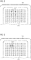
- Fig. 2 illustrates a first exemplary arrangement of a plurality of second light-emitting elements 112-i in the display device 110.
- four second light-emitting elements are illustrated for facilitating the description of the underlaying arrangement scheme.
- more or less second light-emitting elements may be used as well.
- the plurality of first light-emitting elements 111-i and the plurality of second light-emitting elements 112-i are arranged adjacent to each other in rows and columns of an array.
- One first light-emitting element of the plurality of first light-emitting elements 111-i is arranged between each two successive second light-emitting elements of the plurality of second light-emitting elements 112-i in order to avoid larger dark spots on the display device 110.
- two or more first light-emitting element of the plurality of first light-emitting elements 111-i may be arranged between each two successive second light-emitting elements.
- first light-emitting elements 111-i are replaced in the array by second light-emitting elements 112-i.
- the first light-emitting elements 111-i form RGB pixels for displaying the optical image, some of them may be replaced in the display array by, e.g., micro LEDs forming the second light-emitting elements 112-i.
- each first light-emitting element of a first subset of the plurality of first light-emitting elements comprises two light-emitting sub-elements (circuitries, devices) each configured to emit a different one of red, blue and green light, and additionally a respective one of the plurality of second light-emitting elements.
- each first light-emitting element of the first subset is only able to emit light in two different colors among the group of red, blue and green light.
- Each first light-emitting element of a second subset of the plurality of the first light-emitting elements comprises at least three light-emitting sub-elements each configured to emit a different one of red, blue and green light.
- the first light-emitting elements of the second subset do not comprise one of the plurality of second light-emitting elements.
- At least one first light-emitting element of the second subset may be arranged between each two successive first light-emitting elements of the first subset in order to avoid larger dark spots on the display device 110.
- Fig. 3 illustrates a second exemplary arrangement of a plurality of second light-emitting elements 112-i in the display device 110.
- four second light-emitting elements are again illustrated for facilitating the description of the underlaying arrangement scheme.
- more or less second light-emitting elements may be used as well.
- the plurality of first light-emitting elements 111-i are arranged in rows and columns of an array.
- the plurality of second light-emitting elements 112-i are arranged in different lines of the array between columns of the array.
- the first and second light-emitting elements 111-i, 112-i are arranged according to respective arrays.
- a column of the array of the second light-emitting elements 112-i is arranged between two consecutive columns of the array of the first light-emitting elements 111-i.
- a line of the array of the second light-emitting elements 112-i coincides with a line of the array of the first light-emitting elements 111-i.
- the plurality of second light-emitting elements 112-i may analogously be arranged in different columns of the array between lines of the array.
- the first and second light-emitting elements 111-i, 112-i are arranged according to respective arrays.
- a line of the array of the second light-emitting elements 112-i is arranged between two consecutive lines of the array of the first light-emitting elements 111-i.
- a column of the array of the second light-emitting elements 112-i coincides with a column of the array of the first light-emitting elements 111-i.
- the first light-emitting elements 111-i form RGB pixels for displaying the optical image
- micro LEDs forming the second light-emitting elements 112-i may be arranged between the RGB pixels.
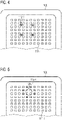
- Fig. 4 illustrates a third exemplary arrangement of a plurality of second light-emitting elements 112-i in the display device 110.
- four second light-emitting elements are again illustrated for facilitating the description of the underlaying arrangement scheme.
- more or less second light-emitting elements may be used as well.
- the plurality of first light-emitting elements 111-i are again arranged in rows and columns of an array.
- the plurality of second light-emitting elements 112-i are arranged between different lines of the array and between different columns of the array.
- the first and second light-emitting elements 111-i, 112-i are arranged according to respective arrays.
- a column, respectively a line of the array of the second light-emitting elements 112-i is arranged between two consecutive columns, respectively two consecutive lines of the array of the first light-emitting elements 111-i.
- first light-emitting elements 111-i form RGB pixels for displaying the optical image
- micro LEDs forming the second light-emitting elements 112-i may be located between the RGB pixels.
- positions of the RGB pixels may be slightly shifted to accommodate for the required space for the micro LEDs.
- Fig. 5 illustrates a fourth exemplary arrangement of a plurality of second light-emitting elements 112-i in the display device 110.
- eight second light-emitting elements are illustrated for facilitating the description of the underlaying arrangement scheme. However, it is to be noted that more or less second light-emitting elements may be used as well.
- the plurality of second light-emitting elements 112-i are arranged in a generally circular pattern.
- the circular pattern of second light-emitting elements 112-i surrounds a region of the display device 110 behind which the optical sensor 120 (in particular its imager) is arranged. Accordingly, shadows of the second light-emitting elements 112-i on the sensed object(s) may be minimized.
- other patterns may be used for the plurality of second light-emitting elements 112-i to surround the region of the display device 110 behind which the optical sensor 120 is arranged (e.g. a rectangle pattern or an irregular pattern).
- the plurality of first light-emitting elements 111-i and the plurality of second light-emitting elements 112-i are arranged adjacent to each other in rows and columns of an array.
- the proposed technique is not limited thereto.
- the plurality of first light-emitting elements 111-i may be again arranged in rows and columns of the array, whereas the plurality of second light-emitting elements 112-i may be arranged in different lines of the array between columns of the array, or in different columns of the array between lines of the array, or between different lines of the array and between different columns of the array to form the circular pattern.
- a circular pattern of RGB pixels may be provided where one of the RGB sub-pixel is respectively replaced by one of the plurality of second light-emitting elements. That is, each first light-emitting element of a first subset of the plurality of first light-emitting elements may comprise two light-emitting sub-elements (circuitries, devices) each configured to emit a respective one of red, blue and green light, and additionally comprise a respective one of the plurality of second light-emitting elements. The first light-emitting elements of the first subset are arranged in a circular pattern.
- Each first light-emitting element of a second subset of the plurality of the first light-emitting elements comprises at least three light-emitting sub-elements each configured to emit a respective one of red, blue and green light.
- the first light-emitting elements of the second subset do not comprise one of the plurality of second light-emitting elements.
- Fig. 6 illustrates a fifth exemplary arrangement of a plurality of second light-emitting elements 112-i in the display device 110.
- four second light-emitting elements are illustrated for facilitating the description of the underlaying arrangement scheme.
- more or less second light-emitting elements may be used as well.
- the plurality of second light-emitting elements 112-i are clustered, i.e. they are arranged as group in the display device 110.
- the clustered second light-emitting elements 112-i may be placed next to a region of the display device 110 at which the optical sensor 120 (in particular its imager) is arranged at the backside of the display device 110.
- This may allow to facilitate control of the second light-emitting elements 112-i as the enable signal for all second light-emitting elements 112-i of the cluster may be provided via a single signal line from a control circuitry. Accordingly, a highly synchronized light emission of the second light-emitting elements 112-i in the cluster may be achieved. This may, in particular, be beneficial if a ToF sensor is used as the optical sensor 120.
- the plurality of first light-emitting elements 111-i and the plurality of second light-emitting elements 112-i are arranged adjacent to each other in rows and columns of an array.
- the proposed technique is not limited thereto.
- the plurality of first light-emitting elements 111-i may be again arranged in rows and columns of the array, whereas the plurality of second light-emitting elements 112-i may be arranged in different lines of the array between columns of the array, or in different columns of the array between lines of the array, or between different lines of the array and between different columns of the array to form the circular pattern.
- Fig. 7 illustrates a sixth exemplary arrangement of a plurality of second light-emitting elements 112-i in the display device 110.
- the plurality of first light-emitting elements 111-i are arranged in rows and columns of an array.
- Each first light-emitting element of a first subset of the plurality of first light-emitting elements 111-i comprises at least three light-emitting sub-elements each configured to (selectively) emit a different one of red, blue and green light, and additionally comprises a respective one of the plurality of second light-emitting elements 112-i.
- each first light-emitting element of a second subset of the plurality of first light-emitting elements 111-i comprises at least three light-emitting sub-elements each configured to (selectively) emit a different one of red, blue and green light.
- the first light-emitting elements of the second subset do not comprise one of the plurality of second light-emitting elements.
- the first light-emitting elements of the second subset may be arranged at a region of the display device 110 at which the optical sensor 120 (in particular its imager) is arranged at the backside of the display device 110.
- the first light-emitting elements of the first subset may be arranged in the remaining region of the display device 110 so as to surround the region of the display device 110 at which the optical sensor 120 is arranged at the backside of the display device 110. Accordingly, shadows of the second light-emitting elements 112-i on the sensed object(s) and stray light (i.e. light reflected by the optical sensor 120) may be minimized.
- the first light-emitting elements of the first subset are not implemented as simple RGB pixels but as RGB-Infrared pixels.
- the display region covering the optical sensor does not feature infrared pixels to increase transparency and limit stray light.
- each RGB pixel may feature and additional infrared sub-pixel. That is, the plurality of first light-emitting elements are again arranged in rows and columns of an array similar to what is illustrated in Fig. 7 . However, in contrast to what is illustrated in Fig. 7 , each of the plurality of first light-emitting elements comprises at least three light-emitting sub-elements each configured to emit a different one of red, blue and green light, and additionally a respective one of the plurality of second light-emitting elements.
- the examples as described herein may be summarized as follows: Some examples relate to a display device.
- the display device comprises a plurality of first light-emitting elements configured to emit light for displaying an optical image on a front side of the display device. Additionally, the display device comprises at least one second light-emitting element configured to emit infrared light for illuminating a scene in front of the front side of the display device.
- the at least one second light-emitting element comprises a micro light emitting diode or a mini light emitting diode configured to emit the infrared light.
- the at least one second light-emitting element comprises: a micro light emitting diode or a mini light emitting diode configured to emit non-infrared light; and a wavelength conversion element configured to convert the non-infrared light emitted by the micro light emitting diode or the mini light emitting diode to the infrared light.
- the wavelength conversion element is a quantum dot.
- the at least one second light-emitting element comprises: a vertical-cavity surface-emitting laser, a micro light emitting diode or a mini light emitting diode configured to emit the infrared light; and an optical element configured to diffuse the infrared light emitted by the vertical-cavity surface-emitting laser, the micro light emitting diode or the mini light emitting diode.
- the at least one second light-emitting element is a light-guiding element, wherein a first end of the light-guiding element is configured to receive the infrared light from a light-source external to the display device, and wherein a second end of the light-guiding element is configured to emit the infrared light for illuminating the scene.
- an optical element is formed on the second end of the light-guiding element and configured to diffuse the infrared light emitted by the second end of the light-guiding element.
- the display device comprises a plurality of second light-emitting elements, wherein the plurality of first light-emitting elements are arranged in rows and columns of an array, and wherein the plurality of second light-emitting elements are arranged: in different lines of the array between columns of the array; or in different columns of the array between lines of the array; or between different lines of the array and between different columns of the array.
- the display device comprises a plurality of second light-emitting elements, wherein the plurality of first light-emitting elements and the plurality of second light-emitting elements are arranged adjacent to each other in rows and columns of an array.
- At least one first light-emitting element of the plurality of first light-emitting elements is arranged between each two successive second light-emitting elements of the plurality of second light-emitting elements.
- the display device comprises a plurality of second light-emitting elements, wherein the plurality of first light-emitting elements are arranged in rows and columns of an array, wherein each first light-emitting element of a first subset of the plurality of first light-emitting elements comprises: either two light-emitting sub-elements each configured to emit a different one of red, blue and green light or at least three light-emitting sub-elements each configured to emit a different one of red, blue and green light; and a respective one of the plurality of second light-emitting elements, wherein each first light-emitting element of a second subset of the plurality of first light-emitting elements comprises at least three light-emitting sub-elements each configured to emit a different one of red, blue and green light, wherein the first light-emitting elements of the second subset do not comprise one of the plurality of second light-emitting elements.
- At least one first light-emitting element of the second subset is arranged between each two successive first light-emitting elements of the first subset.
- the plurality of second light-emitting elements are arranged in a circular pattern.
- the plurality of second light-emitting elements are clustered.
- the display device comprises a plurality of second light-emitting elements, wherein the plurality of first light-emitting elements are arranged in rows and columns of an array, wherein each of the plurality of first light-emitting elements comprises: at least three light-emitting sub-elements each configured to emit a different one of red, blue and green light; and a respective one of the plurality of second light-emitting elements.
- the display device comprises a plurality of second light-emitting elements, wherein at least one of the plurality of second light-emitting elements is configured to emit the infrared light with a first wavelength, and wherein at least one other of the plurality of second light-emitting elements is configured to emit the infrared light with a different second wavelength.
- the display device further comprises control circuitry configured to control the at least one second light-emitting element to emit the infrared light synchronous to the light emission by the plurality of first light-emitting elements.
- the electronic device comprises a display device as proposed herein and at least one optical sensor configured to measure reflected infrared light from the scene.
- the display device is arranged between the at least one optical sensor and the scene.
- the at least one optical sensor is a time-of-flight sensor.
- the at least one optical sensor comprises processing circuitry configured to determine, based on the reflected infrared light from the scene, at least one of an image of at least part of the scene or a distance of the electronic device to at least one object in the scene.
- the optical sensor is configured to measure the reflected infrared light synchronous to a refresh rate of the display device.
- the electronic device comprises a plurality of optical sensors.
- the electronic device is one of a smartphone, a tablet-computer and a laptop-computer.
- Examples of the present disclosure may provide an infrared camera illumination unit embedded in display.
- small infrared LEDs may be integrated into a display device in order to use them as illumination source for image sensors behind the display.
- aspects described in relation to a device or system should also be understood as a description of the corresponding method.
- a block, device or functional aspect of the device or system may correspond to a feature, such as a method step, of the corresponding method.
- aspects described in relation to a method shall also be understood as a description of a corresponding block, a corresponding element, a property or a functional feature of a corresponding device or a corresponding system.
Landscapes
- Engineering & Computer Science (AREA)
- Physics & Mathematics (AREA)
- Electromagnetism (AREA)
- General Physics & Mathematics (AREA)
- Computer Networks & Wireless Communication (AREA)
- Radar, Positioning & Navigation (AREA)
- Remote Sensing (AREA)
- Signal Processing (AREA)
- Optics & Photonics (AREA)
- Condensed Matter Physics & Semiconductors (AREA)
- Devices For Indicating Variable Information By Combining Individual Elements (AREA)
- Environmental & Geological Engineering (AREA)
- Human Computer Interaction (AREA)
- Led Device Packages (AREA)
- Control Of Indicators Other Than Cathode Ray Tubes (AREA)
Claims (16)
- Eine elektronische Vorrichtung (100), umfassend:eine Anzeigevorrichtung (110), die Anzeigevorrichtung (110) umfassend: eine Mehrzahl von ersten lichtemittierenden Elementen (111-i), die ausgebildet ist, um Licht zu emittieren, um ein optisches Bild auf einer Vorderseite (113) der Anzeigevorrichtung (110) anzuzeigen; undzumindest ein zweites lichtemittierendes Element (112-i), das ausgebildet ist, um Infrarotlicht (114) zu emittieren, um eine Szene (190) vor der Vorderseite (113) der Anzeigevorrichtung (110) zu beleuchten;dadurch gekennzeichnet, dass die elektronische Vorrichtung ferner umfasst:zumindest einen Laufzeit-, ToF, Sensor (120), der ausgebildet ist, um einen Bruchteil des emittierten Infrarotlichts (114') zu messen, der von der Szene (190) zurückreflektiert wird,wobei die Anzeigevorrichtung (110) zwischen dem zumindest einen ToF-Sensor (120) und der Szene (190) angeordnet ist, sodass das von der Szene (190) zurückreflektierte Infrarotlicht (114') durch die Anzeigevorrichtung (110) übertragen wird, bevor es den zumindest einen ToF-Sensor (120) erreicht.
- Die elektronische Vorrichtung gemäß Anspruch 1, wobei das zumindest eine zweite lichtemittierende Element (112-i) eine Mikro-Leuchtdiode oder eine Mini-Leuchtdiode umfasst, die ausgebildet ist, um das Infrarotlicht (114) zu emittieren.
- Die elektronische Vorrichtung gemäß Anspruch 1, das zumindest eine zweite lichtemittierende Element (112-i) umfassend:eine Mikro-Leuchtdiode oder eine Mini-Leuchtdiode, die ausgebildet ist, um Nicht-Infrarotlicht zu emittieren; undein Wellenlängenumwandlungselement, das ausgebildet ist, um das von der Mikro-Leuchtdiode oder der Mini-Leuchtdiode emittierte Nicht-Infrarotlicht in das Infrarotlicht (114) umzuwandeln.
- Die elektronische Vorrichtung gemäß Anspruch 1, das zumindest eine zweite lichtemittierende Element (112-i) umfassend:einen oberflächenemittierenden Diodenlaser, eine Mikro-Leuchtdiode oder eine Mini-Leuchtdiode, die ausgebildet sind, um das Infrarotlicht (114) zu emittieren; undein optisches Element, das ausgebildet ist, um das von dem oberflächenemittierenden Diodenlaser, der Mikro-Leuchtdiode oder der Mini-Leuchtdiode emittierte Infrarotlicht (114) zu streuen.
- Die elektronische Vorrichtung gemäß Anspruch 1, wobei das zumindest eine zweite lichtemittierende Element (112-i) ein lichtleitendes Element ist, wobei ein erstes Ende des lichtleitenden Elements ausgebildet ist, um das Infrarotlicht (114) von einer Lichtquelle außerhalb der Anzeigevorrichtung (110) zu empfangen und wobei ein zweites Ende des lichtleitenden Elements ausgebildet ist, um das Infrarotlicht (114) zum Beleuchten der Szene (190) zu emittieren.
- Die elektronische Vorrichtung gemäß einem der Ansprüche 1 bis 5, wobei die Anzeigevorrichtung (110) eine Mehrzahl von zweiten lichtemittierenden Elementen (112-i) umfasst, wobei die Mehrzahl von ersten lichtemittierenden Elementen (111-i) in Reihen und Spalten eines Arrays angeordnet ist und wobei die Mehrzahl von zweiten lichtemittierenden Elementen (112-i) wie folgt angeordnet ist:in unterschiedlichen Zeilen des Arrays zwischen Spalten des Arrays; oderin unterschiedlichen Spalten des Arrays zwischen Zeilen des Arrays; oderzwischen unterschiedlichen Zeilen des Arrays und zwischen unterschiedlichen Spalten des Arrays.
- Die elektronische Vorrichtung gemäß einem der Ansprüche 1 bis 5, wobei die Anzeigevorrichtung (110) eine Mehrzahl von zweiten lichtemittierenden Elementen (112-i) umfasst, wobei die Mehrzahl von ersten lichtemittierenden Elementen (111-i) und die Mehrzahl von zweiten lichtemittierenden Elementen (112-i) benachbart zueinander in Reihen und Spalten eines Arrays angeordnet sind.
- Die elektronische Vorrichtung gemäß Anspruch 7, wobei zumindest ein erstes lichtemittierendes Element aus der Mehrzahl von ersten lichtemittierenden Elementen (111-i) zwischen jeweils zwei aufeinanderfolgenden zweiten lichtemittierenden Elementen aus der Mehrzahl von zweiten lichtemittierenden Elementen (112-i) angeordnet ist.
- Die elektronische Vorrichtung gemäß einem der Ansprüche 1 bis 5, wobei die Anzeigevorrichtung (110) eine Mehrzahl von zweiten lichtemittierenden Elementen (112-i) umfasst, wobei die Mehrzahl von ersten lichtemittierenden Elementen (111-i) in Reihen und Spalten eines Arrays angeordnet ist, wobei jedes erste lichtemittierende Element einer ersten Teilmenge aus der Mehrzahl von ersten lichtemittierenden Elementen (111-i) umfasst:entweder zwei lichtemittierende Teilelemente, die jeweils ausgebildet sind, um ein unterschiedliches von rotem, blauem und grünem Licht zu emittieren, oder zumindest drei lichtemittierende Teilelemente, die jeweils ausgebildet sind, um ein unterschiedliches von rotem, blauem und grünem Licht zu emittieren; undein jeweiliges aus der Mehrzahl von zweiten lichtemittierenden Elementen (112-i),wobei jedes erste lichtemittierende Element einer zweiten Teilmenge aus der Mehrzahl von ersten lichtemittierenden Elementen (111-i) zumindest drei lichtemittierende Teilelemente umfasst, die jeweils ausgebildet sind, um ein unterschiedliches von rotem, blauem und grünem Licht zu emittieren, wobei die ersten lichtemittierenden Elemente der zweiten Teilmenge nicht eines aus der Mehrzahl von zweiten lichtemittierenden Elementen (112-i) umfassen.
- Die elektronische Vorrichtung gemäß Anspruch 9, wobei zumindest ein erstes lichtemittierendes Element aus der zweiten Teilmenge zwischen jeweils zwei aufeinanderfolgenden ersten lichtemittierenden Elementen aus der ersten Teilmenge angeordnet ist.
- Die elektronische Vorrichtung gemäß einem der Ansprüche 6 bis 10, wobei die Mehrzahl von zweiten lichtemittierenden Elementen (112-i) eine Region der Anzeigevorrichtung (110) umgibt, hinter der ein optischer Sensor angeordnet ist.
- Die elektronische Vorrichtung gemäß einem der Ansprüche 6 bis 10, wobei die Mehrzahl von zweiten lichtemittierenden Elementen (112-i) geclustert ist.
- Die elektronische Vorrichtung gemäß einem der Ansprüche 1 bis 5, wobei die Anzeigevorrichtung (110) eine Mehrzahl von zweiten lichtemittierenden Elementen (112-i) umfasst, wobei die Mehrzahl von ersten lichtemittierenden Elementen (111-i) in Reihen und Spalten eines Arrays angeordnet ist, wobei jedes aus der Mehrzahl von ersten lichtemittierenden Elementen (111-i) umfasst:zumindest drei lichtemittierende Teilelemente, die jeweils ausgebildet sind, um ein unterschiedliches von rotem, blauem und grünem Licht zu emittieren; undein jeweiliges aus der Mehrzahl von zweiten lichtemittierenden Elementen (112-i).
- Die elektronische Vorrichtung gemäß einem der Ansprüche 1 bis 13, wobei die Anzeigevorrichtung (110) eine Mehrzahl von zweiten lichtemittierenden Elementen (112-i) umfasst, wobei zumindest eines aus der Mehrzahl von zweiten lichtemittierenden Elementen (112-i) ausgebildet ist, um das Infrarotlicht (114) mit einer ersten Wellenlänge zu emittieren und wobei zumindest ein anderes aus der Mehrzahl von zweiten lichtemittierenden Elementen (112-i) ausgebildet ist, um das Infrarotlicht (114) mit einer unterschiedlichen zweiten Wellenlänge zu emittieren.
- Die elektronische Vorrichtung gemäß einem der Ansprüche 1 bis 14, wobei die Anzeigevorrichtung (110) ferner eine Steuerschaltungsanordnung umfasst, die ausgebildet ist, um das zumindest eine zweite lichtemittierende Element (112-i) zu steuern, um das Infrarotlicht (114) synchron zu der Lichtemission durch die Mehrzahl von ersten lichtemittierenden Elementen (111-i) zu emittieren.
- Die elektronische Vorrichtung gemäß einem der Ansprüche 1 bis 15, wobei der zumindest eine ToF-Sensor (120) ausgebildet ist, um das von der Szene (190) zurückreflektierte Infrarotlicht (114') synchron zu einer Aktualisierungsrate der Anzeigevorrichtung (110) zu messen.
Priority Applications (3)
| Application Number | Priority Date | Filing Date | Title |
|---|---|---|---|
| EP20207106.4A EP4002455B1 (de) | 2020-11-12 | 2020-11-12 | Anzeigevorrichtung und elektronische vorrichtung damit |
| CN202111331329.2A CN114500700B (zh) | 2020-11-12 | 2021-11-11 | 显示设备和包括该显示设备的电子设备 |
| US17/524,023 US12431470B2 (en) | 2020-11-12 | 2021-11-11 | Display device and electronic device including the display device |
Applications Claiming Priority (1)
| Application Number | Priority Date | Filing Date | Title |
|---|---|---|---|
| EP20207106.4A EP4002455B1 (de) | 2020-11-12 | 2020-11-12 | Anzeigevorrichtung und elektronische vorrichtung damit |
Publications (2)
| Publication Number | Publication Date |
|---|---|
| EP4002455A1 EP4002455A1 (de) | 2022-05-25 |
| EP4002455B1 true EP4002455B1 (de) | 2022-10-12 |
Family
ID=73401337
Family Applications (1)
| Application Number | Title | Priority Date | Filing Date |
|---|---|---|---|
| EP20207106.4A Active EP4002455B1 (de) | 2020-11-12 | 2020-11-12 | Anzeigevorrichtung und elektronische vorrichtung damit |
Country Status (3)
| Country | Link |
|---|---|
| US (1) | US12431470B2 (de) |
| EP (1) | EP4002455B1 (de) |
| CN (1) | CN114500700B (de) |
Families Citing this family (6)
| Publication number | Priority date | Publication date | Assignee | Title |
|---|---|---|---|---|
| CN109451106B (zh) * | 2018-11-16 | 2020-06-12 | Oppo广东移动通信有限公司 | 电子装置 |
| IT202000019543A1 (it) * | 2020-08-06 | 2022-02-06 | Goffi Alberto Mario | Sistema di controllo di accessi e/o presenze |
| KR20230085421A (ko) * | 2021-12-07 | 2023-06-14 | 엘지디스플레이 주식회사 | 표시장치 |
| CN119068757A (zh) | 2023-06-01 | 2024-12-03 | 群创光电股份有限公司 | 电子装置与车用显示装置 |
| TWI854679B (zh) * | 2023-06-01 | 2024-09-01 | 群創光電股份有限公司 | 電子裝置與車用顯示裝置 |
| US20240423545A1 (en) * | 2023-06-22 | 2024-12-26 | Stmicroelectronics International N.V. | Non-invasive vital signs monitoring on a mobile device using an under-display optical sensor |
Family Cites Families (23)
| Publication number | Priority date | Publication date | Assignee | Title |
|---|---|---|---|---|
| WO2014197109A2 (en) * | 2013-03-22 | 2014-12-11 | Seiko Epson Corporation | Infrared video display eyewear |
| US10713458B2 (en) * | 2016-05-23 | 2020-07-14 | InSyte Systems | Integrated light emitting display and sensors for detecting biologic characteristics |
| KR102335714B1 (ko) * | 2016-10-24 | 2021-12-06 | 글로 에이비 | 발광 다이오드, 디스플레이 소자 및 직시형 디스플레이 소자 |
| WO2018100082A1 (en) * | 2016-11-30 | 2018-06-07 | Sony Semiconductor Solutions Corporation | Apparatus and method |
| GB201700530D0 (en) * | 2017-01-12 | 2017-03-01 | Purelifi Ltd | Display apparatus |
| US10664676B2 (en) * | 2017-06-12 | 2020-05-26 | Will Semiconductor (Shanghai) Co. Ltd. | Systems and methods for reducing unwanted reflections in display systems incorporating an under display biometric sensor |
| US11417806B2 (en) * | 2018-07-30 | 2022-08-16 | Lumileds Llc | Dielectric mirror for broadband IR LEDs |
| DE102018119548A1 (de) * | 2018-08-10 | 2020-02-13 | Osram Opto Semiconductors Gmbh | Anzeigevorrichtung |
| CN111081694B (zh) * | 2018-10-18 | 2022-03-22 | 群创光电股份有限公司 | 电子装置、拼接电子设备与其操作方法 |
| CN113508260B (zh) * | 2019-01-09 | 2023-11-10 | 亮锐控股有限公司 | 用于显示屏的背光照明的照明设备 |
| US10838556B2 (en) * | 2019-04-05 | 2020-11-17 | Apple Inc. | Sensing system for detection of light incident to a light emitting layer of an electronic device display |
| CN112242415B (zh) * | 2019-07-18 | 2025-03-11 | 群创光电股份有限公司 | 电子装置 |
| KR102812110B1 (ko) * | 2019-08-30 | 2025-05-27 | 엘지이노텍 주식회사 | Tof 카메라 |
| CN111902822B (zh) * | 2019-08-30 | 2024-06-21 | 深圳市汇顶科技股份有限公司 | 利用外部光源的屏下照明 |
| CN112468615A (zh) * | 2019-09-09 | 2021-03-09 | 北京小米移动软件有限公司 | 电子设备 |
| US11417796B2 (en) * | 2019-12-03 | 2022-08-16 | Lumileds Llc | Light-emitting apparatus including a reflective cavity |
| US11508700B2 (en) * | 2019-12-10 | 2022-11-22 | Meta Platforms Technologies, Llc | Left and right projectors for display device |
| KR102870007B1 (ko) * | 2020-02-11 | 2025-10-13 | 삼성디스플레이 주식회사 | 표시 장치 |
| CN111627346A (zh) * | 2020-06-16 | 2020-09-04 | 武汉华星光电技术有限公司 | 一种显示面板及显示装置 |
| US11749964B2 (en) * | 2020-06-24 | 2023-09-05 | Meta Platforms Technologies, Llc | Monolithic light source with integrated optics based on nonlinear frequency conversion |
| KR102843470B1 (ko) * | 2020-07-30 | 2025-08-08 | 삼성디스플레이 주식회사 | 표시장치 |
| JP7547914B2 (ja) * | 2020-10-12 | 2024-09-10 | Toppanホールディングス株式会社 | 空中表示装置 |
| EP4002813B1 (de) * | 2020-11-12 | 2024-10-09 | Infineon Technologies AG | Sensor positioniert hinter einem mikro-led-bereich innerhalb eines oled-displays |
-
2020
- 2020-11-12 EP EP20207106.4A patent/EP4002455B1/de active Active
-
2021
- 2021-11-11 US US17/524,023 patent/US12431470B2/en active Active
- 2021-11-11 CN CN202111331329.2A patent/CN114500700B/zh active Active
Also Published As
| Publication number | Publication date |
|---|---|
| CN114500700B (zh) | 2026-01-09 |
| US12431470B2 (en) | 2025-09-30 |
| US20220149016A1 (en) | 2022-05-12 |
| CN114500700A (zh) | 2022-05-13 |
| EP4002455A1 (de) | 2022-05-25 |
Similar Documents
| Publication | Publication Date | Title |
|---|---|---|
| EP4002455B1 (de) | Anzeigevorrichtung und elektronische vorrichtung damit | |
| CN117173998B (zh) | 显示装置 | |
| US12193291B2 (en) | Display substrate and display device | |
| JP6564019B2 (ja) | ピクセル数の多い表示装置用の有色無機ledディスプレイ | |
| US8502756B2 (en) | Image display device with imaging unit | |
| US8274034B2 (en) | Optical arrangement comprising emitters and detectors on a common substrate | |
| JP6141347B2 (ja) | 光源装置及び表示装置 | |
| US10190746B1 (en) | Optical lens for beam shaping and steering and devices using the optical lens | |
| EP3467811A1 (de) | Anzeigebildschirm | |
| US12176331B2 (en) | Electronic device | |
| WO2020233684A1 (zh) | 一种显示屏及电子设备 | |
| CN108121932A (zh) | 有机发光二极管显示屏指纹识别装置及电子设备 | |
| WO2018040774A1 (zh) | 基板、显示面板及显示装置 | |
| US20230288194A1 (en) | Miniature Pattern Projector Using Microleds And Micro-Optics | |
| JP2012008169A (ja) | 画像表示装置、電子機器、測定治具、画像表示システム、画像表示方法、表示補正装置、表示補正方法、プログラム | |
| US11796858B2 (en) | Backlight substrate, manufacturing method thereof and display device | |
| WO2020140532A1 (zh) | 光源模组和显示模组 | |
| CN108899356B (zh) | Oled显示基板及其制作方法、显示装置 | |
| CN108960196B (zh) | 指纹识别结构和显示面板 | |
| JP4464412B2 (ja) | 面状光源装置及びそれを用いた液晶表示装置 | |
| EP4001957B1 (de) | Elektronische vorrichtung mit im display integrierter beleuchtungseinheit und entsprechendes steuerungsverfahren | |
| US20240292717A1 (en) | Display device | |
| EP4001989B1 (de) | Elektronische vorrichtung und verfahren für eine elektronische vorrichtung | |
| CN101520581B (zh) | 显示装置及其显示基板 |
Legal Events
| Date | Code | Title | Description |
|---|---|---|---|
| PUAI | Public reference made under article 153(3) epc to a published international application that has entered the european phase |
Free format text: ORIGINAL CODE: 0009012 |
|
| STAA | Information on the status of an ep patent application or granted ep patent |
Free format text: STATUS: REQUEST FOR EXAMINATION WAS MADE |
|
| 17P | Request for examination filed |
Effective date: 20210723 |
|
| AK | Designated contracting states |
Kind code of ref document: A1 Designated state(s): AL AT BE BG CH CY CZ DE DK EE ES FI FR GB GR HR HU IE IS IT LI LT LU LV MC MK MT NL NO PL PT RO RS SE SI SK SM TR |
|
| GRAP | Despatch of communication of intention to grant a patent |
Free format text: ORIGINAL CODE: EPIDOSNIGR1 |
|
| STAA | Information on the status of an ep patent application or granted ep patent |
Free format text: STATUS: GRANT OF PATENT IS INTENDED |
|
| RIC1 | Information provided on ipc code assigned before grant |
Ipc: H01S 5/183 20060101ALN20220516BHEP Ipc: H01L 31/12 20060101ALN20220516BHEP Ipc: H01L 33/50 20100101ALN20220516BHEP Ipc: H01L 25/16 20060101ALN20220516BHEP Ipc: H01L 25/075 20060101AFI20220516BHEP |
|
| INTG | Intention to grant announced |
Effective date: 20220601 |
|
| GRAS | Grant fee paid |
Free format text: ORIGINAL CODE: EPIDOSNIGR3 |
|
| GRAA | (expected) grant |
Free format text: ORIGINAL CODE: 0009210 |
|
| STAA | Information on the status of an ep patent application or granted ep patent |
Free format text: STATUS: THE PATENT HAS BEEN GRANTED |
|
| AK | Designated contracting states |
Kind code of ref document: B1 Designated state(s): AL AT BE BG CH CY CZ DE DK EE ES FI FR GB GR HR HU IE IS IT LI LT LU LV MC MK MT NL NO PL PT RO RS SE SI SK SM TR |
|
| REG | Reference to a national code |
Ref country code: GB Ref legal event code: FG4D |
|
| REG | Reference to a national code |
Ref country code: CH Ref legal event code: EP |
|
| REG | Reference to a national code |
Ref country code: DE Ref legal event code: R096 Ref document number: 602020005582 Country of ref document: DE |
|
| REG | Reference to a national code |
Ref country code: IE Ref legal event code: FG4D |
|
| REG | Reference to a national code |
Ref country code: AT Ref legal event code: REF Ref document number: 1524687 Country of ref document: AT Kind code of ref document: T Effective date: 20221115 |
|
| REG | Reference to a national code |
Ref country code: LT Ref legal event code: MG9D |
|
| REG | Reference to a national code |
Ref country code: NL Ref legal event code: MP Effective date: 20221012 |
|
| REG | Reference to a national code |
Ref country code: AT Ref legal event code: MK05 Ref document number: 1524687 Country of ref document: AT Kind code of ref document: T Effective date: 20221012 |
|
| PG25 | Lapsed in a contracting state [announced via postgrant information from national office to epo] |
Ref country code: NL Free format text: LAPSE BECAUSE OF FAILURE TO SUBMIT A TRANSLATION OF THE DESCRIPTION OR TO PAY THE FEE WITHIN THE PRESCRIBED TIME-LIMIT Effective date: 20221012 |
|
| PG25 | Lapsed in a contracting state [announced via postgrant information from national office to epo] |
Ref country code: SE Free format text: LAPSE BECAUSE OF FAILURE TO SUBMIT A TRANSLATION OF THE DESCRIPTION OR TO PAY THE FEE WITHIN THE PRESCRIBED TIME-LIMIT Effective date: 20221012 Ref country code: PT Free format text: LAPSE BECAUSE OF FAILURE TO SUBMIT A TRANSLATION OF THE DESCRIPTION OR TO PAY THE FEE WITHIN THE PRESCRIBED TIME-LIMIT Effective date: 20230213 Ref country code: NO Free format text: LAPSE BECAUSE OF FAILURE TO SUBMIT A TRANSLATION OF THE DESCRIPTION OR TO PAY THE FEE WITHIN THE PRESCRIBED TIME-LIMIT Effective date: 20230112 Ref country code: LT Free format text: LAPSE BECAUSE OF FAILURE TO SUBMIT A TRANSLATION OF THE DESCRIPTION OR TO PAY THE FEE WITHIN THE PRESCRIBED TIME-LIMIT Effective date: 20221012 Ref country code: FI Free format text: LAPSE BECAUSE OF FAILURE TO SUBMIT A TRANSLATION OF THE DESCRIPTION OR TO PAY THE FEE WITHIN THE PRESCRIBED TIME-LIMIT Effective date: 20221012 Ref country code: ES Free format text: LAPSE BECAUSE OF FAILURE TO SUBMIT A TRANSLATION OF THE DESCRIPTION OR TO PAY THE FEE WITHIN THE PRESCRIBED TIME-LIMIT Effective date: 20221012 Ref country code: AT Free format text: LAPSE BECAUSE OF FAILURE TO SUBMIT A TRANSLATION OF THE DESCRIPTION OR TO PAY THE FEE WITHIN THE PRESCRIBED TIME-LIMIT Effective date: 20221012 |
|
| PG25 | Lapsed in a contracting state [announced via postgrant information from national office to epo] |
Ref country code: RS Free format text: LAPSE BECAUSE OF FAILURE TO SUBMIT A TRANSLATION OF THE DESCRIPTION OR TO PAY THE FEE WITHIN THE PRESCRIBED TIME-LIMIT Effective date: 20221012 Ref country code: PL Free format text: LAPSE BECAUSE OF FAILURE TO SUBMIT A TRANSLATION OF THE DESCRIPTION OR TO PAY THE FEE WITHIN THE PRESCRIBED TIME-LIMIT Effective date: 20221012 Ref country code: LV Free format text: LAPSE BECAUSE OF FAILURE TO SUBMIT A TRANSLATION OF THE DESCRIPTION OR TO PAY THE FEE WITHIN THE PRESCRIBED TIME-LIMIT Effective date: 20221012 Ref country code: IS Free format text: LAPSE BECAUSE OF FAILURE TO SUBMIT A TRANSLATION OF THE DESCRIPTION OR TO PAY THE FEE WITHIN THE PRESCRIBED TIME-LIMIT Effective date: 20230212 Ref country code: HR Free format text: LAPSE BECAUSE OF FAILURE TO SUBMIT A TRANSLATION OF THE DESCRIPTION OR TO PAY THE FEE WITHIN THE PRESCRIBED TIME-LIMIT Effective date: 20221012 Ref country code: GR Free format text: LAPSE BECAUSE OF FAILURE TO SUBMIT A TRANSLATION OF THE DESCRIPTION OR TO PAY THE FEE WITHIN THE PRESCRIBED TIME-LIMIT Effective date: 20230113 |
|
| P01 | Opt-out of the competence of the unified patent court (upc) registered |
Effective date: 20230528 |
|
| REG | Reference to a national code |
Ref country code: DE Ref legal event code: R097 Ref document number: 602020005582 Country of ref document: DE |
|
| REG | Reference to a national code |
Ref country code: BE Ref legal event code: MM Effective date: 20221130 |
|
| PG25 | Lapsed in a contracting state [announced via postgrant information from national office to epo] |
Ref country code: SM Free format text: LAPSE BECAUSE OF FAILURE TO SUBMIT A TRANSLATION OF THE DESCRIPTION OR TO PAY THE FEE WITHIN THE PRESCRIBED TIME-LIMIT Effective date: 20221012 Ref country code: RO Free format text: LAPSE BECAUSE OF FAILURE TO SUBMIT A TRANSLATION OF THE DESCRIPTION OR TO PAY THE FEE WITHIN THE PRESCRIBED TIME-LIMIT Effective date: 20221012 Ref country code: MC Free format text: LAPSE BECAUSE OF FAILURE TO SUBMIT A TRANSLATION OF THE DESCRIPTION OR TO PAY THE FEE WITHIN THE PRESCRIBED TIME-LIMIT Effective date: 20221012 Ref country code: EE Free format text: LAPSE BECAUSE OF FAILURE TO SUBMIT A TRANSLATION OF THE DESCRIPTION OR TO PAY THE FEE WITHIN THE PRESCRIBED TIME-LIMIT Effective date: 20221012 Ref country code: DK Free format text: LAPSE BECAUSE OF FAILURE TO SUBMIT A TRANSLATION OF THE DESCRIPTION OR TO PAY THE FEE WITHIN THE PRESCRIBED TIME-LIMIT Effective date: 20221012 Ref country code: CZ Free format text: LAPSE BECAUSE OF FAILURE TO SUBMIT A TRANSLATION OF THE DESCRIPTION OR TO PAY THE FEE WITHIN THE PRESCRIBED TIME-LIMIT Effective date: 20221012 |
|
| PLBE | No opposition filed within time limit |
Free format text: ORIGINAL CODE: 0009261 |
|
| STAA | Information on the status of an ep patent application or granted ep patent |
Free format text: STATUS: NO OPPOSITION FILED WITHIN TIME LIMIT |
|
| PG25 | Lapsed in a contracting state [announced via postgrant information from national office to epo] |
Ref country code: SK Free format text: LAPSE BECAUSE OF FAILURE TO SUBMIT A TRANSLATION OF THE DESCRIPTION OR TO PAY THE FEE WITHIN THE PRESCRIBED TIME-LIMIT Effective date: 20221012 Ref country code: LU Free format text: LAPSE BECAUSE OF NON-PAYMENT OF DUE FEES Effective date: 20221112 Ref country code: AL Free format text: LAPSE BECAUSE OF FAILURE TO SUBMIT A TRANSLATION OF THE DESCRIPTION OR TO PAY THE FEE WITHIN THE PRESCRIBED TIME-LIMIT Effective date: 20221012 |
|
| 26N | No opposition filed |
Effective date: 20230713 |
|
| PG25 | Lapsed in a contracting state [announced via postgrant information from national office to epo] |
Ref country code: IE Free format text: LAPSE BECAUSE OF NON-PAYMENT OF DUE FEES Effective date: 20221112 |
|
| PG25 | Lapsed in a contracting state [announced via postgrant information from national office to epo] |
Ref country code: SI Free format text: LAPSE BECAUSE OF FAILURE TO SUBMIT A TRANSLATION OF THE DESCRIPTION OR TO PAY THE FEE WITHIN THE PRESCRIBED TIME-LIMIT Effective date: 20221012 Ref country code: BE Free format text: LAPSE BECAUSE OF NON-PAYMENT OF DUE FEES Effective date: 20221130 |
|
| PG25 | Lapsed in a contracting state [announced via postgrant information from national office to epo] |
Ref country code: CY Free format text: LAPSE BECAUSE OF FAILURE TO SUBMIT A TRANSLATION OF THE DESCRIPTION OR TO PAY THE FEE WITHIN THE PRESCRIBED TIME-LIMIT Effective date: 20221012 |
|
| PG25 | Lapsed in a contracting state [announced via postgrant information from national office to epo] |
Ref country code: MK Free format text: LAPSE BECAUSE OF FAILURE TO SUBMIT A TRANSLATION OF THE DESCRIPTION OR TO PAY THE FEE WITHIN THE PRESCRIBED TIME-LIMIT Effective date: 20221012 Ref country code: IT Free format text: LAPSE BECAUSE OF FAILURE TO SUBMIT A TRANSLATION OF THE DESCRIPTION OR TO PAY THE FEE WITHIN THE PRESCRIBED TIME-LIMIT Effective date: 20221012 |
|
| PG25 | Lapsed in a contracting state [announced via postgrant information from national office to epo] |
Ref country code: TR Free format text: LAPSE BECAUSE OF FAILURE TO SUBMIT A TRANSLATION OF THE DESCRIPTION OR TO PAY THE FEE WITHIN THE PRESCRIBED TIME-LIMIT Effective date: 20221012 |
|
| REG | Reference to a national code |
Ref country code: CH Ref legal event code: PL |
|
| PG25 | Lapsed in a contracting state [announced via postgrant information from national office to epo] |
Ref country code: CH Free format text: LAPSE BECAUSE OF NON-PAYMENT OF DUE FEES Effective date: 20231130 |
|
| PG25 | Lapsed in a contracting state [announced via postgrant information from national office to epo] |
Ref country code: HU Free format text: LAPSE BECAUSE OF FAILURE TO SUBMIT A TRANSLATION OF THE DESCRIPTION OR TO PAY THE FEE WITHIN THE PRESCRIBED TIME-LIMIT; INVALID AB INITIO Effective date: 20201112 Ref country code: CH Free format text: LAPSE BECAUSE OF NON-PAYMENT OF DUE FEES Effective date: 20231130 Ref country code: BG Free format text: LAPSE BECAUSE OF FAILURE TO SUBMIT A TRANSLATION OF THE DESCRIPTION OR TO PAY THE FEE WITHIN THE PRESCRIBED TIME-LIMIT Effective date: 20221012 |
|
| PG25 | Lapsed in a contracting state [announced via postgrant information from national office to epo] |
Ref country code: MT Free format text: LAPSE BECAUSE OF FAILURE TO SUBMIT A TRANSLATION OF THE DESCRIPTION OR TO PAY THE FEE WITHIN THE PRESCRIBED TIME-LIMIT Effective date: 20221012 |
|
| REG | Reference to a national code |
Ref country code: DE Ref legal event code: R079 Ref document number: 602020005582 Country of ref document: DE Free format text: PREVIOUS MAIN CLASS: H01L0025075000 Ipc: H10H0029240000 |
|
| PGFP | Annual fee paid to national office [announced via postgrant information from national office to epo] |
Ref country code: GB Payment date: 20251121 Year of fee payment: 6 |
|
| PGFP | Annual fee paid to national office [announced via postgrant information from national office to epo] |
Ref country code: FR Payment date: 20251126 Year of fee payment: 6 |
|
| PGFP | Annual fee paid to national office [announced via postgrant information from national office to epo] |
Ref country code: DE Payment date: 20260121 Year of fee payment: 6 |