EP4002472A1 - Panneau d'affichage transmettant la lumière, panneau d'affichage et appareil d'affichage - Google Patents
Panneau d'affichage transmettant la lumière, panneau d'affichage et appareil d'affichage Download PDFInfo
- Publication number
- EP4002472A1 EP4002472A1 EP20906853.5A EP20906853A EP4002472A1 EP 4002472 A1 EP4002472 A1 EP 4002472A1 EP 20906853 A EP20906853 A EP 20906853A EP 4002472 A1 EP4002472 A1 EP 4002472A1
- Authority
- EP
- European Patent Office
- Prior art keywords
- light
- transmitting
- sub
- display panel
- pixel
- Prior art date
- Legal status (The legal status is an assumption and is not a legal conclusion. Google has not performed a legal analysis and makes no representation as to the accuracy of the status listed.)
- Pending
Links
Images




Classifications
-
- H—ELECTRICITY
- H10—SEMICONDUCTOR DEVICES; ELECTRIC SOLID-STATE DEVICES NOT OTHERWISE PROVIDED FOR
- H10K—ORGANIC ELECTRIC SOLID-STATE DEVICES
- H10K59/00—Integrated devices, or assemblies of multiple devices, comprising at least one organic light-emitting element covered by group H10K50/00
- H10K59/10—OLED displays
- H10K59/12—Active-matrix OLED [AMOLED] displays
- H10K59/121—Active-matrix OLED [AMOLED] displays characterised by the geometry or disposition of pixel elements
-
- H—ELECTRICITY
- H10—SEMICONDUCTOR DEVICES; ELECTRIC SOLID-STATE DEVICES NOT OTHERWISE PROVIDED FOR
- H10K—ORGANIC ELECTRIC SOLID-STATE DEVICES
- H10K50/00—Organic light-emitting devices
- H10K50/80—Constructional details
- H10K50/805—Electrodes
- H10K50/81—Anodes
- H10K50/818—Reflective anodes, e.g. ITO combined with thick metallic layers
-
- H—ELECTRICITY
- H10—SEMICONDUCTOR DEVICES; ELECTRIC SOLID-STATE DEVICES NOT OTHERWISE PROVIDED FOR
- H10K—ORGANIC ELECTRIC SOLID-STATE DEVICES
- H10K59/00—Integrated devices, or assemblies of multiple devices, comprising at least one organic light-emitting element covered by group H10K50/00
- H10K59/30—Devices specially adapted for multicolour light emission
- H10K59/35—Devices specially adapted for multicolour light emission comprising red-green-blue [RGB] subpixels
- H10K59/353—Devices specially adapted for multicolour light emission comprising red-green-blue [RGB] subpixels characterised by the geometrical arrangement of the RGB subpixels
-
- H—ELECTRICITY
- H10—SEMICONDUCTOR DEVICES; ELECTRIC SOLID-STATE DEVICES NOT OTHERWISE PROVIDED FOR
- H10K—ORGANIC ELECTRIC SOLID-STATE DEVICES
- H10K59/00—Integrated devices, or assemblies of multiple devices, comprising at least one organic light-emitting element covered by group H10K50/00
- H10K59/60—OLEDs integrated with inorganic light-sensitive elements, e.g. with inorganic solar cells or inorganic photodiodes
-
- H—ELECTRICITY
- H10—SEMICONDUCTOR DEVICES; ELECTRIC SOLID-STATE DEVICES NOT OTHERWISE PROVIDED FOR
- H10K—ORGANIC ELECTRIC SOLID-STATE DEVICES
- H10K59/00—Integrated devices, or assemblies of multiple devices, comprising at least one organic light-emitting element covered by group H10K50/00
- H10K59/80—Constructional details
- H10K59/805—Electrodes
- H10K59/8051—Anodes
- H10K59/80518—Reflective anodes, e.g. ITO combined with thick metallic layers
-
- H—ELECTRICITY
- H10—SEMICONDUCTOR DEVICES; ELECTRIC SOLID-STATE DEVICES NOT OTHERWISE PROVIDED FOR
- H10K—ORGANIC ELECTRIC SOLID-STATE DEVICES
- H10K2102/00—Constructional details relating to the organic devices covered by this subclass
- H10K2102/10—Transparent electrodes, e.g. using graphene
- H10K2102/101—Transparent electrodes, e.g. using graphene comprising transparent conductive oxides [TCO]
- H10K2102/103—Transparent electrodes, e.g. using graphene comprising transparent conductive oxides [TCO] comprising indium oxides, e.g. ITO
-
- H—ELECTRICITY
- H10—SEMICONDUCTOR DEVICES; ELECTRIC SOLID-STATE DEVICES NOT OTHERWISE PROVIDED FOR
- H10K—ORGANIC ELECTRIC SOLID-STATE DEVICES
- H10K59/00—Integrated devices, or assemblies of multiple devices, comprising at least one organic light-emitting element covered by group H10K50/00
- H10K59/60—OLEDs integrated with inorganic light-sensitive elements, e.g. with inorganic solar cells or inorganic photodiodes
- H10K59/65—OLEDs integrated with inorganic image sensors
Definitions
- the application relates to the field of display, and particularly to a light-transmitting display panel, display panel and display apparatus.
- the present application provides a light-transmitting display panel, display panel and display apparatus, enabling at least some regions of the display panel to transmit light as well as display, so as to facilitate under-screen integration of photosensitive components.
- an embodiment of the present application provides a light-transmitting display panel.
- the light-transmitting display panel includes a first pixel array including a first minimum repeating unit.
- the first minimum repeating unit includes at least one light-transmitting column unit.
- the at least one light-transmitting column unit has a central axis parallel to an extending direction of the at least one light-transmitting column unit.
- the at least one light-transmitting column unit includes a plurality of first sub-pixels spaced apart from one another in the extending direction of the light-transmitting column unit, wherein at least one of the first sub-pixels in the at least one light-transmitting column unit is set to deviate from the central axis.
- photosensitive components may be integrated on the back of the light-transmitting display panel to achieve under-screen integration of the photosensitive components such as cameras, while the light-transmitting display panel can display pictures, so as to achieve a full-screen design in which the light-transmitting display panel is applied to a display apparatus.
- each light-transmitting column unit includes a plurality of first sub-pixels spaced apart from one another in the extending direction of the light-transmitting column unit. At least one of the first sub-pixels in the at least one light-transmitting column unit is set to deviate from the central axis, so as to avoid a strictly and neatly collinear arrangement of each column of first sub-pixels in the first pixel array and reduce arrangement consistency of the first sub-pixels, and thus to reduce a diffraction effect on light of the light-transmitting display panel.
- the quality of images obtained by the photosensitive components integrated on the back of the light-transmitting display panel can be improved, and the resolution and contrast of the images obtained by the photosensitive components can be improved, by reducing the diffraction effect on light of the light-transmitting display panel.
- the plurality of first sub-pixels in the at least one light-transmitting column unit are arranged into a curved arrangement structure.
- a length of a first electrode in a direction parallel to the central axis is 10 to 35 microns, and a length of the first electrode in a direction perpendicular to the central axis is 10 to 35 microns.
- an embodiment of the present application provides a display panel.
- the display panel includes a first display area and a second display area adjacent to each other.
- a light transmittance of the first display area is greater than a light transmittance of the second display area.
- the first display area of the display panel is configured to be the light-transmitting display panel of any of the forgoing implementations.
- the display panel further includes a second pixel array disposed in the second display area.
- the second pixel array includes a second minimum repeating unit.
- the second minimum repeating unit includes a plurality of opaque column units.
- Each of the opaque column units includes a plurality of second sub-pixels spaced apart from one another in an extending direction of the opaque column unit.
- the extending direction of the opaque column unit is same as the extending direction of the light-transmitting column unit.
- the at least one light-transmitting column unit of the first minimum repeating unit includes a plurality of light-transmitting column units.
- the plurality of second sub-pixels included in each of the opaque column units are set collinearly in the extending direction of the opaque column unit.
- a number of opaque column units in the second minimum repeating unit is the same as a number of light-transmitting column units in the first minimum repeating unit and each light-transmitting column unit and corresponding one of the opaque column units have a same shape, and in the light-transmitting column unit and the corresponding opaque column unit, the plurality of first sub-pixels and the plurality of second sub-pixels have a same color sequence.
- an embodiment of the present application provides a display apparatus, including the light-transmitting display panel of any of the forgoing implementations.
- photosensitive components may be integrated on the back of the light-transmitting display panel to achieve under-screen integration of the photosensitive components such as cameras, while the light-transmitting display panel can display pictures, so as to achieve a full-screen design in which the light-transmitting display panel is applied to a display apparatus.
- each light-transmitting column unit includes a plurality of first sub-pixels spaced apart from one another in the extending direction of the light-transmitting column unit. At least one of the first sub-pixels in the at least one light-transmitting column unit is set to deviate from the central axis, so as to avoid a strictly and neatly collinear arrangement of each column of first sub-pixels in the first pixel array and reduce arrangement consistency of the first sub-pixels, and thus to reduce a diffraction effect on light of the light-transmitting display panel.
- the quality of images obtained by the photosensitive components integrated on the back of the light-transmitting display panel can be improved, and the resolution and contrast of the images obtained by the photosensitive components can be improved, by reducing the diffraction effect on light of the light-transmitting display panel.
- the plurality of first sub-pixels in the at least one light-transmitting column unit are arranged in a curved arrangement structure. Therefore, the diffraction effect on light of the light-transmitting display panel can be reduced and the quality of images obtained by the photosensitive components integrated on the back of the light-transmitting display panel can be further improved, by optimizing relative positions of the first sub-pixels.
- relationship terms such as first, second, and the like are used herein simply to distinguish one entity or operation from another entity or operation, but do not necessarily require or imply any actual such relationship or order between these entities or operations.
- an electronic device such as a mobile phone and a tablet etc.
- photosensitive components e.g., front-facing cameras, infrared light sensors, and proximity light sensors
- a light-transmitting display area may be provided on the above-described electronic device, and the photosensitive components may be arranged on the back of the light-transmitting display area, such that all-screen display for the electronic device can be achieved, while proper operations of the photosensitive components can be guaranteed
- patterned structures such as anodes and wires etc. will cause a diffraction phenomenon of light.
- the diffraction phenomenon causes directly a degradation in quality of images captured by the photosensitive components.
- the multi-order diffraction spots may enter the photosensitive components and may be captured by the photosensitive components, resulting in a decline in image resolution and contrast.
- embodiments of the present application provide a light-transmitting display panel, display panel and display apparatus.
- Various embodiments of the light-transmitting display panel, display panel and display apparatus will be described below in connection with the accompanying drawings.
- Embodiments of the present application provide a light-transmitting display panel, which may be an Organic Light Emitting Diode (Organic Light Emitting Diode, OLED) display panel.
- a light-transmitting display panel which may be an Organic Light Emitting Diode (Organic Light Emitting Diode, OLED) display panel.
- OLED Organic Light Emitting Diode
- the "light-transmitting display panel” used herein refers to a display panel with light transmittance greater than or equal to 15%. In order to ensure that the light transmittance of the light-transmitting display panel is greater than or equal to 15%, or even greater than 40% or more, light transmittance of at least some of functional film layers of the light-transmitting display panel in the embodiments of the present application is greater than 80%, or even greater than 90%.
- Fig. 1 is a schematic top view of a light-transmitting display panel provided by an embodiment of the present application.
- the light-transmitting display panel 100 may include a first pixel array PX1, which includes a first minimum repeating unit RU1.
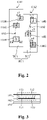
- Fig. 2 is a schematic enlarged view of a first minimum repeating unit of a light-transmitting display panel provided by an embodiment of the present application.
- the first minimum repeating unit RU1 includes at least one light-transmitting column units TC1, TC2.
- the first minimum repeating unit RU1 includes a first light-transmitting column unit TC1 and a second light-transmitting column unit TC2.
- the first pixel array PX1 includes a plurality of first sub-pixels 110 arranged in an array.
- the plurality of first sub-pixels 110 arranged in the array may be arranged in multiple rows and multiple columns.
- An extending direction of the rows crosses an extending direction of the columns.
- the extension direction of the rows may be parallel approximately to an extension direction of gate lines (scanning lines) in the light-transmitting display panel 100, and the extension direction of the columns may be substantially parallel to an extension direction of data lines in the light-transmitting display panel 100.
- a light-transmitting column unit refers to a regional unit obtained by further dividing a region occupied by the first minimum repeating unit in the light-transmitting display panel in columns, i.e., the first minimum repeating unit includes at least one column unit that is obtained by dividing the first minimum repeating unit in columns of the first sub-pixels 110 and is light-transmitting. Transmittance of the column unit may indicate particularly that at least a part region of the column unit can transmit light.
- the column unit may include an emitting area corresponding to the first sub-pixel 110 and a non-emitting area surrounding the emitting area. The non-emitting area may transmit light, and the emitting area may or may not transmit light.
- a number of light-transmitting column units included in each first minimum repeating unit RU1 is not limited to two as described above, and may be more.
- photosensitive components may be integrated on the back of the light-transmitting display panel 100, to achieve under-screen integration of the photosensitive components such as cameras, while the light-transmitting display panel 100 can display pictures, so as to achieve a full-screen design in which the light-transmitting display panel 100 is applied to a display apparatus.
- the light-transmitting column units TC1, TC2 respectively have the central axes CA1, CA2 parallel to an extending direction of the light-transmitting column unit TC1, TC2.
- the at least one light-transmitting column unit TC1, TC2 includes a plurality of first sub-pixels 110 spaced apart from one another in the extending direction of the light-transmitting column units TC1, TC2.
- the first light-transmitting column unit TC1 has the central axis CA1 parallel to the extending direction of the first light-transmitting column unit TC1
- the second light-transmitting column unit TC2 has the central axis CA2 parallel to the extending direction of the first light-transmitting column unit TC2.
- At least one of the first sub-pixels 110 in the at least one light-transmitting column unit is set to deviate from the central axis, so as to avoid a strictly and neatly collinear arrangement of each column of first sub-pixels 110 in the first pixel array PX1 and reduce arrangement consistency of the first sub-pixels 110, and thus to reduce a diffraction effect on light of the light-transmitting display panel 100.
- the quality of images obtained by the photosensitive components integrated on the back of the light-transmitting display panel 100 can be improved, and the resolution and contrast of the images obtained by the photosensitive components can be improved, by reducing the diffraction effect on light of the light-transmitting display panel 100.
- each of center points of the first sub-pixels 110 is shown as a solid dot.
- arrangement of positions of the sub-pixels refers particularly arrangement of positions of the center points of the sub-pixels.
- a first sub-pixels 110 being set to deviate from the central axis means that the center point of the first sub-pixel 110 is set to deviate from the central axis.
- the plurality of first sub-pixels 110 in at least one light-transmitting column unit TC are arranged in a curved arrangement structure. In some embodiments, the plurality of first sub-pixels 110 in the at least one light-transmitting column unit TC are arranged in an arcuate arrangement structure AS.
- the first light-transmitting column unit TC1 includes a first sub-pixel 110R, a first sub-pixel 110G, and a first sub-pixel 110B that are spaced apart from one another in the extending direction of the first light-transmitting column unit TC1.
- the first sub-pixel 110R is a red sub-pixel
- the first sub-pixel 110G is a green sub-pixel
- the first sub-pixel 110B is a blue sub-pixel.
- the first sub-pixel 110R is set to deviate from the central axis CA1. Particularly, as shown in Fig.
- the first sub-pixel 110R is set to deviate rightward from the central axis CA1, and a distance from the first sub-pixel 110R of the first light-transmitting column unit TC1 to the central axis CA1 is 18.87 microns.
- the second light-transmitting column unit TC2 includes a first sub-pixel 110B, a first sub-pixel 110R, and first sub-pixel 110G that are spaced from one another in the extending direction of the second light-transmitting column unit TC2.
- the first sub-pixel 110R is a red sub-pixel
- the first sub-pixel 110G is a green sub-pixel
- the first sub-pixel 110B is a blue sub-pixel.
- the first sub-pixel 110B, the first sub-pixel 110R, and the first sub-pixel 110G are all set to deviate from the central axis CA2. Particularly, as shown in Fig.
- the first sub-pixel 110B is set to deviate rightward from the central axis CA2, and a distance y2 from the first sub-pixel 110B of the second light-transmitting column unit TC2 to the central axis CA2 is 10.38 microns.
- the first sub-pixel 110R is set to deviate leftward from the central axis CA2, and a distance y3 from the first sub-pixel 110R of the second light-transmitting column unit TC2 to the central axis CA2 is 9.87 microns.
- the first sub-pixel 110G is set to deviate rightward from the central axis CA2, and a distance y4 from the first sub-pixel 110G of the second light-transmitting column unit TC2 to the central axis CA2 is 9.87 microns.
- first sub-pixels 110 By arranging the plurality of first sub-pixels 110 in the at least one light-transmitting column unit into a curved arrangement structure, relative positions of the first sub-pixels 110 can be optimized, such that the diffraction effect on light of the light-transmitting display panel 100 can be reduced, and the quality of images obtained by the photosensitive components integrated on the back of the light-transmitting display panel 100 can be further improved.
- a distance from a first sub-pixel 110 that is set to deviate from a central axis to the central axis ranges from 3 to 35 microns.
- the first sub-pixels 110 may include red sub-pixels, green sub-pixels, and blue sub-pixels.
- red sub-pixel When a red sub-pixel is set to deviate from a central axis, a distance from its center point to the corresponding central axis ranges from 3 to 35 microns.
- a green sub-pixel is set to deviate from a central axis, a distance from its center point to the corresponding central axis ranges from 3 to 30 microns.
- a blue sub-pixel is set to deviate from a central axis, a distance from its center point to the corresponding central axis ranges from 3 to 30 microns.
- the plurality of first sub-pixels 110 of at least two light-transmitting column units TC1, TC2 are arranged in an arcuate arrangement structure.
- Arcuate arrangement structures respectively corresponding to the light-transmitting column units TC1, TC2 have a same arcuate convex direction.
- the plurality of first sub-pixels 110 of the first light-transmitting column unit TC1 are arranged in a first arcuate arrangement structure AS1
- the plurality of first sub-pixels 110 of the second light-transmitting column unit TC2 are arranged in a second arcuate arrangement structure AS2
- an arcuate convex direction of the first arcuate arrangement structure AS 1 and an arcuate convex direction of the second arcuate arrangement structure AS2 are both leftward.
- the plurality of first sub-pixels 110 of the at least two light-transmitting column units TC1, TC2 are arranged in an arcuate arrangement structure.
- Arcuate arrangement structures respectively corresponding to the light-transmitting column units of the light-transmitting column units TC1, TC2 are different from each other.
- the first arcuate arrangement structure AS 1 and the second arcuate arrangement structure AS2 are not completely the same as each other in shape.
- Fig. 3 is a schematic cross-sectional view along a Z-Z direction shown in Fig. 2 .
- the light-transmitting display panel 100 includes a substrate 101, a device layer 102 and a pixel definition layer 103.
- the device layer 102 is disposed on the substrate 101, and the pixel definition layer 103 is disposed on the device layer 102.
- the substrate 101 maybe made of light-transmitting materials such as glass, polyimide (Polyimide, PI, or the like.
- the device layer 102 may include pixel circuits for driving respective sub-pixels to display.
- the pixel defining layer 103 may include pixel openings.
- Each first sub-pixel 110 includes a first electrode 111 disposed on the substrate 101, a first light-emitting structure 112 disposed on the first electrode 111, and a second electrode 113 disposed on the first light-emitting structure 112.
- the first electrode 111 is disposed on the device layer 102 and may be electrically connected to the pixel circuits in the device layer 102.
- the first light-emitting structure 112 may be disposed in a corresponding pixel opening.
- the first electrode 111 may be a reflective electrode, so as to improve a display effect of the formed first sub-pixel 110.
- the reflective electrode includes a first light-transmitting conductive layer, a reflective layer disposed on the first light-transmitting conductive layer, and a second light-transmitting conductive layer disposed on the reflective layer.
- the first light-transmitting conductive layer and the second light-transmitting conductive layer may be indium tin oxide (Indium Tin Oxide, ITO) layers or indium zinc oxide (Indium Zinc Oxide, IZO) layers, etc.
- the reflective layer may be a metal layer, such as being made of silver.
- the second electrode 113 may be a magnesium-silver alloy layer.
- the first light-emitting structure 112 may include an emitting layer (Emitting Layer, EML). According to design requirements of the first light-emitting structure 112, the first light-emitting structure 112 may further include at least one of a hole inject layer (Hole Inject Layer, HIL), a hole transport layer (Hole Transport Layer, HTL), and an electron inject layer (Electron Inject Layer, EIL), or an electron transport layer (Electron Transport Layer, ETL).
- HIL hole inject Layer
- HTL hole transport layer
- EIL electron inject layer
- ETL electron transport layer
- an orthographic projection of each first electrode 111 on the substrate 101 may comprise one first graphic unit or two or more first graphic units connected together.
- the first graphic unit may include at least one selected from a group of a circle, an oval, a dumbbell shape, a gourd shape, and a rectangle.
- the orthographic projection of the first electrode 111 on the substrate 101 is a rectangle.
- an orthographic projection of each first light-emitting structure 112 on the substrate 101 may comprise one second graphic unit or two or more second graphic units connected together.
- the second graphic unit include at least one selected from a group of a circle, an oval, a dumbbell shape, a gourd shape, and a rectangle.
- the orthographic projection of the first light light-emitting structure 112 on the substrate 101 is a rectangle.
- a length of the first electrode 111 in a direction parallel to the central axis CA is 10 to 35 microns, and a length of the first electrode 111 in a direction perpendicular to the central axis CA is 10 to 35 microns.
- the size of the first electrode 111 can be reduced while the display effect can be guaranteed. As a result, the diffraction phenomenon on light of the light-transmitting display panel 100 can be reduced.
- Fig. 4 is a diagram showing energy distribution of diffraction spots generated by performing diffraction detection on the light-transmitting display panel 100 provided by the embodiment of the present application.
- Fig. 4 shows the energy distribution of diffraction spots on a part of the light-transmitting display panel 100.
- Fig. 5 is a schematic structural diagram of a comparative minimum repeating unit in a pixel array included in a light-transmitting display panel provided by the comparative embodiment.
- Column units included in the comparative minimum repeating unit RU0 are the same as the light-transmitting column units included in first minimum repeating unit RU1 of the foregoing embodiment, in number, shape and size.
- Sub-pixels in each column unit are the same as the first sub-pixels 110 in the corresponding light-transmitting column unit, in number and color.
- the comparative minimum repeating unit RU0 includes a first column unit TC1' and a second column unit TC2'.
- the first column unit TC1' has a central axis CA1' parallel to an extending direction of the first column unit TC1'
- the second column unit TC2' has a central axis CA2' parallel to an extending direction of the second column cell TC2'.
- Comparative pixels 110R', 110G', 110B' in the first column unit TC1' are all located along the central axis CA1'
- comparative pixels 110B', 110R', 110G' in the second column unit TC2' are all located along the central axis CA2'.
- the other structures of the comparative minimum repeating unit RU0 are substantially the same as those of the first minimum repeating unit RU1 of the foregoing embodiment.
- Fig. 6 is a diagram showing energy distribution of diffraction spots generated by performing diffraction detection on the light-transmitting display panel provided by the comparative embodiment.
- Fig. 6 shows the energy distribution of diffraction spots on a part of the light-transmitting display panel provided by the comparative embodiment.
- a ratio of energy of level 1 of a diffraction spot to energy of level 0 of a diffraction spot is 1.298%
- ratios of energy of level 2 of two diffraction spots to energy of level 0 of diffraction spot are 1.01%, 1.075%, respectively.
- ratios of energy of level 1 of two diffraction spots to energy of level 0 of a diffraction spot are 0.536%, 0.552%, respectively, and ratios of energy of level 2 of two diffraction spots to energy of level 0 of a diffraction spot are 0.212%, 0.242%, respectively.
- the quality of images obtained by the photosensitive components integrated on the back of the light-transmitting display panel 100 can be further improved, by optimizing relative positions of the first sub-pixels 110 to reduce the diffraction effect on light of the light-transmitting display panel 100.
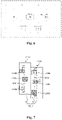
- Fig. 7 a schematic enlarged view of a first minimum repeating unit of a light-transmitting display panel provided by an alternative embodiment of the present application.
- the first minimum repeating unit RU1 includes a first light-transmitting column unit TC1 and a second light-transmitting column unit TC2.
- the first light-transmitting column unit TC1 has a central axis CA1 parallel to an extending direction of the first light-transmitting column unit TC1
- the second light-transmitting column unit TC2 has a central axis CA2 parallel to an extending direction of the second light-transmitting column unit TC2.
- the first light-transmitting column unit TC1 includes a first sub-pixel 110R, a first sub-pixel 110G, and a first sub-pixel 110B that are spaced from one another in the extending direction of the first light-transmitting column unit TC1.
- the first sub-pixel 110R is a red sub-pixel
- the first sub-pixel 110G is a green sub-pixel
- the first sub-pixel 110B is a blue sub-pixel.
- the first sub-pixel 110R and the first sub-pixel 110B are set to deviate from the central axis CA1. Particularly, as shown in Fig.
- the first sub-pixel 110R is set to deviate leftward from the central axis CA1, and a distance y5 from the first sub-pixel 110R of the first light-transmitting column unit TC1 to the central axis CA1 is 12.13 microns.
- the first sub-pixel 110B is set to deviate leftward from the central axis CA1, and a distance y6 from the first sub-pixel 110B of the first light-transmitting column unit TC1 to the central axis CA1 is 11.37 microns.
- the second light-transmitting column unit TC2 includes a first sub-pixel 110B, a first sub-pixel 110R, and first sub-pixel 110G that are spaced from one another in the extending direction of the second light-transmitting column unit TC2.
- the first sub-pixel 110R is a red sub-pixel
- the first sub-pixel 110G is a green sub-pixel
- the first sub-pixel 110B is a blue sub-pixel.
- the first sub-pixel 110B, the first sub-pixel 110R, and the first sub-pixel 110G are all are all set to deviate from the central axis CA2. Particularly, as shown in Fig.
- the first sub-pixel 110B is set to deviate leftward from the central axis CA2, and a distance y7 from the first sub-pixel 110B of the second light-transmitting column unit TC2 to the central axis CA2 is 12.62 microns.
- the first sub-pixel 110R is set to deviate leftward from the central axis CA2, and a distance y8 from the first sub-pixel 110R of the second light-transmitting column unit TC2 to the central axis CA2 is 9.87 microns.
- the first sub-pixel 110G is set to deviate leftward from the central axis CA2, and a distance y9 from the first sub-pixel 110G of the second light-transmitting column unit TC2 to the central axis CA2 is 11.63 microns.
- the plurality of first sub-pixels 110 of the first light-transmitting column unit TC1 are arranged in a first arcuate arrangement structure AS1, and the plurality of first sub-pixels 110 of the second light-transmitting column unit TC2 are arranged in a second arcuate arrangement structure AS2.
- Arcuate arrangement structures respectively corresponding to the light-transmitting column units TC1, TC2 have a same arcuate convex direction.
- an arcuate convex direction of the first arcuate arrangement structure AS 1 and an arcuate convex direction of the second arcuate arrangement structure AS2 are both rightward.
- Fig. 8 is a diagram showing energy distribution of diffraction spots generated by performing diffraction detection on the light-transmitting display panel provided by the alternative embodiment of the present application.
- Fig. 8 shows the energy distribution of diffraction spots on a part of the light-transmitting display panel provided by the alternative embodiment.
- ratios of energy of level 1 of two diffraction spots to energy of level 0 of a diffraction spot are 0.383%, 0.397%, respectively, and a ratio of energy of level 2 of a diffraction spot to energy of level 0 of diffraction spot is 0.320%.
- the quality of images obtained by the photosensitive components integrated on the back of the light-transmitting display panel 100 can be further improved, by arranging the plurality of first sub-pixels 110 in the at least one light-transmitting column unit in an arcuate arrangement structure, so as to optimize relative positions of the first sub-pixels 110 and thus reduce the diffraction effect on light of the light-transmitting display panel 100.
- Embodiment of the present application also provides a display panel.
- the display panel of the embodiments of the present application will be described below.
- Fig. 9 is a schematic top view of a display panel provided by an embodiment of the present application.
- the display panel 1000 has a first display area AA1 and a second display area AA2 adjacent to each other.
- the display panel 1000 may further include a non-display area NA surrounding the first display area AA1 and the second display area AA2.
- a light transmittance of the first display area AA1 is greater than a light transmittance of the second display area AA2.
- the first display area AA1 of the display panel 1000 may be configured as the light-transmitting display panel 100 provided according to any one of the foregoing embodiments of the present application. In this embodiment, it is used as an example for illustration that the first display area AA1 of the display panel 1000 is configured as the light-transmitting display panel 100 provided in the foregoing embodiment of the present application.
- Fig. 10 is a schematic enlarged partial view of a Q region shown in Fig. 9 .
- the display panel 1000 includes a first pixel array PX1 in the first display area AA1, and the first pixel array PX1 includes a first minimum repeating unit RU1.
- a structure of the first minimum repeat unit RU1 in this embodiment may refer to Fig. 2 .
- the first minimum repeating unit RU1 includes at least one light-transmitting column unit TC1, TC2. In this embodiment, it is used as an example for illustration that the first minimum repeating unit RU1 includes a first light-transmitting column unit TC1 and a second light-transmitting column unit TC2.
- the at least one light-transmitting column unit TC1, TC2 has a central axis CA1, CA2 parallel to an extending direction of the light-transmitting column unit TC1, TC2, and the at least one light-transmitting column unit TC1, TC2 includes a plurality of sub-pixels 110 spaced from one another in the extending direction of the first light-transmitting column unit TC1, TC2.
- the first light-transmitting column unit TC1 has a central axis CA1 parallel to the extending direction of the first light-transmitting column unit TC1
- the second light-transmitting column unit TC2 has a central axis CA2 parallel to the extending direction parallel to the second light-transmitting column unit TC2.
- the light transmittance of the first display area AA1 is greater than the light transmittance of the second display area AA2, so that the display panel 1000 may achieve under-screen integration of photosensitive components such as cameras by integrating the photosensitive components on the back of the first display area AA1, while the first display area AA1 can display pictures. Therefore, an area of display of the display panel 1000 can be increased and a full-screen design of a display apparatus can be achieved.
- At least one of the first sub-pixels 110 in the at least one light-transmitting column unit is set to deviate from the central axis, so as to avoid a strictly and neatly collinear arrangement of each column of first sub-pixels 110 in the first pixel array PX1 and reduce arrangement consistency of the first sub-pixels 110, and thus to reduce a diffraction effect on light of the first display area AA1 of the light-transmitting display panel 1000.
- the quality of images obtained by the photosensitive components integrated on the back of the first display area AA1 can be improved, and the resolution and contrast of the images obtained by the photosensitive components can be improved, by reducing the diffraction effect on light of the first display area AA1.
- the display panel 1000 may further include a second pixel array PX2 disposed in the second display area AA2.
- the second pixel array PX2 includes a second minimum repeating unit RU2.
- Fig. 11 is a schematic enlarged view of a first minimum repeating unit of the light-transmitting display panel provided by the embodiment of the present application.
- the second minimum repeating unit RU2 may include at least one opaque column unit NCl, NC2.
- Each opaque column unit NCl, NC2 may include a plurality of second sub-pixels spaced from one another in an extending direction of the opaque column unit NCl, NC2 210.
- the extending direction of the opaque column units NCl, NC2 is the same as the extending direction of the light-transmitting column units TC1, TC2.
- the plurality of second sub-pixels 210 included in each opaque column unit are set collinearly in the extending direction of the opaque column unit.
- each of center points of the second sub-pixels 210 is shown as a hollow dot.
- a number of the opaque column units NCl, NC2 in the second minimum repeating unit RU2 is the same as a number of the light-transmitting column units TC1, TC2 in the first minimum repeating unit RU1, and each opaque column unit NC1, NC2 and corresponding one of the light-transmitting column units TC1, TC2 have a same shape.
- the second minimum repeating unit RU2 includes the first opaque column unit NC1 and the second opaque column unit NC2.
- the first opaque column unit NC1 corresponds to and has the same shape as the first light-transmitting column unit TC1.
- the second opaque column unit NC2 corresponds to and has the same shape as the second light-transmitting column unit TC2.
- the plurality of first sub-pixels 110 and the plurality of second sub-pixels 210 have the same color sequence.
- the first light-transmitting column unit TC1 includes a first sub-pixel 110R, a first sub-pixel 110G, and a first sub-pixel 110B that are spaced from one another in the extending direction of the first light-transmitting column unit TC1.
- the first sub-pixel 110R is a red sub-pixel
- the first sub-pixel 110G is a green sub-pixel
- the first sub-pixel 110B is a blue sub-pixel.
- the first opaque column unit NCl includes a second sub-pixel 210R, a second sub-pixel 210G, and a second sub-pixel 210B that are spaced apart from one another in the extending direction of the first opaque column unit NC1.
- the second sub-pixel 210R is a red sub-pixel
- the second sub-pixel 210G is a green sub-pixel
- the second sub-pixel 210B is a blue sub-pixel. That is, in the first light-transmitting column unit TC1 and the first opaque column unit NCl, the color sequence is red, green, and blue.
- the second light-transmitting column unit TC2 includes a first sub-pixel 110B, a first sub-pixel 110R, and a first sub-pixel 110G that are spaced apart from one another in the extending direction of the second light-transmitting column unit TC2.
- the first sub-pixel 110R is a red sub-pixel
- the first sub-pixel 110G is a green sub-pixel
- the first sub-pixel 110B is a blue sub-pixel.
- the second opaque column unit NC2 includes a second sub-pixel 210B, a second sub-pixel 210R, and a second sub-pixel 210G that are spaced apart from one another in the extending direction of the second opaque column unit NC2.
- the second sub-pixel 210R is a red sub-pixel
- the second sub-pixel 210G is a green sub-pixel
- the second sub-pixel 210B is a blue sub-pixel. That is, in the second light-transmitting column unit TC2 and the second opaque column unit NC2, the color sequence is blue, red, and green.
- Fig. 12 is a schematic projection diagram when the second minimum repeating unit is projected to the first minimum repeating unit in the display panel provided by the embodiment of the present application.
- each of center points of first sub-pixels 110 is shown as a solid dot
- a projection of each of center points of second sub-pixels 210 on a first minimum repeating unit RU1 is shown as a hollow dot.
- 210R", 210G" and 210B" represent projection of a center of a second sub-pixel 210R, a center of a second sub-pixel 210G, and a center of a second sub-pixel 210B on the first minimum repeating unit RU1, respectively.
- projection profiles of the opaque column units NCl, NC2 coincide with profiles of corresponding light-transmitting column units TC1, TC2, when the second minimum repeating unit RU2 is projected to the first minimum repeating unit RU1.
- At least one of the first sub-pixels 110 and a projection of a second sub-pixel at a position corresponding to the second sub-pixel 210 in the color sequence deviate from each other in a direction parallel to the central axis.
- the first sub-pixel 110 and the second sub-pixel 210 at the positions corresponding to each other in the color sequence may be understood as follows.
- the first light-transmitting column unit TC1 and the corresponding first opaque column unit NC1 are taken as examples, in which the color sequence is red, green and blue.
- a first sub-pixel at the red position in the color sequence is the first sub-pixel 110R
- a second sub-pixel at the red position in the color sequence is the second sub-pixel 210R.
- the first sub-pixel 110R and the second sub-pixel 210R are the first sub-pixel 110 and the second sub-pixel 210 at the positions corresponding to each other in the color sequence.
- Other first sub-pixels 110 and second sub-pixels 210 at the positions corresponding to each other in the color sequence may be obtained similarly based on this rule.
- the first sub-pixel 110R of the first light-transmitting column unit TC1 in the first minimum repeating unit RU1 deviates downward from the projection 210R" of the second sub-pixel 210R of the corresponding first opaque column unit NC1 in the direction parallel to the central axis CA1, and a deviation distance x1 is 10.71 microns.
- Other first sub-pixels 110 of the first minimum repeating unit RU1 do not deviate from projections of corresponding second sub-pixels 210.
- a deviation distance between a projection of a first sub-pixel 110 and a projection of the corresponding second sub-pixel 210 deviating from each other in the direction parallel to the central axis CA ranges from 3 to 35 microns.
- the plurality of first sub-pixels 110 of the first light-transmitting column unit TC1 are arranged in a first arcuate arrangement structure AS1
- the plurality of first sub-pixels 110 of the second light-transmitting column unit TC2 are arranged in a second arcuate arrangement structure AS2.
- Convex directions of the first arcuate arrangement structure AS 1 and the second arcuate arrangement structure AS2 are both leftward.
- Fig. 13 is a schematic projection diagram when a second minimum repeating unit is projected to a first minimum repeating unit in a light-transmitting display panel provided by an alternative embodiment of the present application.
- Fig. 13 involves a first minimum repeating unit that may be the first minimum repeating unit in the light-transmitting display panel provided by the alternative embodiment of the present application in Fig. 7 .
- each of center points of first sub-pixels 110 is shown as a solid dot
- a projection of each of center points of second sub-pixels 210 on a first minimum repeating unit RU1 is shown as a hollow dot.
- 210R", 210G" and 210B" represent projection of a center of a second sub-pixel 210R, a center of a second sub-pixel 210G, and a center of a second sub-pixel 210B on the first minimum repeating unit RU1, respectively.
- the color sequence in a first light-transmitting column unit TC1 and a first opaque column unit NC1, the color sequence is red, green and blue. In a second light-transmitting column unit TC2 and a second opaque column unit NC2, the color sequence is blue, red and green.
- a first sub-pixel 110R of the first light-transmitting column unit TC1 deviates downward from the projection 210R" of the second sub-pixel 210R of the corresponding first opaque column unit NC1 in a direction parallel to a central axis CA1, and a deviation distance x2 is 10.71 microns.
- a first sub-pixel 110G of the first light-transmitting column unit TC1 deviates downward from the projection 210G" of the second sub-pixel 210G of the corresponding first opaque column unit NC1 in the direction parallel to the central axis CA1, and a deviation distance x3 is 10 microns.
- a first sub-pixel 110B of the first light-transmitting column unit TC1 does not deviate from the projection 210B" of the second sub-pixel 210B of the corresponding first opaque column unit NC1 in the direction parallel to the central axis CA1.
- a first sub-pixel 110B of the second light-transmitting column unit TC2 does not deviate from the projection 210B" of the second sub-pixel 210B of the corresponding second opaque column unit NC2 in a direction parallel to a central axis CA2.
- a first sub-pixel 110R of the second light-transmitting column unit TC2 deviates upward from the projection 210R" of the second sub-pixel 210R of the corresponding second opaque column unit NC2 in the direction parallel to the central axis CA2, and a deviation distance x4 is 9.43 microns.
- a first sub-pixel 110G of the second light-transmitting column unit TC2 does not deviate from the projection 210G" of the second sub-pixel 210G of the corresponding second opaque column unit NC2 in the direction parallel to the central axis CA2.
- the plurality of first sub-pixels 110 of the first light-transmitting column unit TC1 are arranged in a first arcuate arrangement structure AS1
- the plurality of first sub-pixels 110 of the second light-transmitting column unit TC2 are arranged in a second arcuate arrangement structure AS2.
- Convex directions of the first arcuate arrangement structure AS 1 and the second arcuate arrangement structure AS2 are both rightward.
- the quality of images obtained by photosensitive components integrated on the back of the first display area AA1 of the light-transmitting display panel 100 can be further improved, by arranging the plurality of first sub-pixels 110 in the at least one light-transmitting column unit in an arcuate arrangement structure, so as to optimize relative positions of the first sub-pixels 110 and thus reduce the diffraction effect on light of the first display area AA1.
- An embodiment of the present application further provides a display apparatus, which may include the light-transmitting display panel 100 of any of the foregoing embodiments.
- the light-transmitting display panel 100 includes a display surface and a non-display surface opposite to the display surface.
- the display apparatus may further include photosensitive components disposed on the side of the non-display surface of the light-transmitting display panel 100.
- the photosensitive components may be apparatuses for image acquisition that may be used to acquire external image information.
- the photosensitive components are complementary metal oxide semiconductor (Complementary Metal Oxide Semiconductor, CMOS) apparatuses for image acquisition, and in some other embodiments, the photosensitive components may be other types of apparatuses for image acquisition, such as charge-coupled device (Charge-coupled Device, CCD) apparatuses for image acquisition.
- CMOS complementary metal oxide semiconductor
- CCD Charge-coupled Device
- the photosensitive components may not be limited to the apparatuses for image acquisition, and in some embodiments, the photosensitive components may be light sensors such as infrared sensors or proximity sensors etc., for example.
- photosensitive components may be integrated on the non-display surface of the light-transmitting display panel 100, to achieve under-screen integration of the photosensitive components such as apparatuses for image acquisition, while the light-transmitting display panel 100 can display pictures, so as to achieve a full-screen design of the display apparatus
- the light-transmitting display panel 100 may include a first pixel array PX1, which may include a first minimum repeating unit RU1.
- the first minimum repeating unit RU1 may include at least one light-transmitting column unit TC1, TC2.
- Each light-transmitting column unit TC1, TC2 may have a central axis CA1, CA2 parallel to an extending direction of the light-transmitting column unit TC1, TC2.
- Each light-transmitting column unit TC1, TC2 may include a plurality of first sub-pixels 110 spaced from one another in the extending direction of the first light-transmitting column unit TC1, TC2. At least one of the first sub-pixels 110 in the at least one light-transmitting column unit is set to deviate from the central axis.
- a strictly and neatly collinear arrangement of each column of first sub-pixels 110 in the first pixel array PX1 can be avoided and arrangement consistency of the first sub-pixels 110 can be reduced, and thereby a diffraction effect on light of the light-transmitting display panel 100 can be reduced.
- the quality of images obtained by the photosensitive components integrated on the back of the light-transmitting display panel 100 can be improved, and the resolution and contrast of the images obtained by the photosensitive components can be improved, by reducing the diffraction effect on light of the light-transmitting display panel 100.
- the plurality of first sub-pixels 110 in the at least one light-transmitting column unit are arranged into a curved arrangement structure, and thereby the diffraction effect on light of the light-transmitting display panel 100 can be reduced by optimizing relative positions of the first sub-pixels 110, so as to further improve the quality of images obtained by the photosensitive components in the display apparatus.
Landscapes
- Chemical & Material Sciences (AREA)
- Inorganic Chemistry (AREA)
- Physics & Mathematics (AREA)
- Sustainable Development (AREA)
- Life Sciences & Earth Sciences (AREA)
- Microelectronics & Electronic Packaging (AREA)
- Engineering & Computer Science (AREA)
- Geometry (AREA)
- Optics & Photonics (AREA)
- Devices For Indicating Variable Information By Combining Individual Elements (AREA)
- Electroluminescent Light Sources (AREA)
- Illuminated Signs And Luminous Advertising (AREA)
- Display Devices Of Pinball Game Machines (AREA)
Applications Claiming Priority (2)
| Application Number | Priority Date | Filing Date | Title |
|---|---|---|---|
| CN201911348304.6A CN111029391B (zh) | 2019-12-24 | 2019-12-24 | 透光显示面板、显示面板及显示装置 |
| PCT/CN2020/120402 WO2021129049A1 (fr) | 2019-12-24 | 2020-10-12 | Panneau d'affichage transmettant la lumière, panneau d'affichage et appareil d'affichage |
Publications (2)
| Publication Number | Publication Date |
|---|---|
| EP4002472A1 true EP4002472A1 (fr) | 2022-05-25 |
| EP4002472A4 EP4002472A4 (fr) | 2022-10-26 |
Family
ID=70212002
Family Applications (1)
| Application Number | Title | Priority Date | Filing Date |
|---|---|---|---|
| EP20906853.5A Pending EP4002472A4 (fr) | 2019-12-24 | 2020-10-12 | Panneau d'affichage transmettant la lumière, panneau d'affichage et appareil d'affichage |
Country Status (7)
| Country | Link |
|---|---|
| US (1) | US20220149120A1 (fr) |
| EP (1) | EP4002472A4 (fr) |
| JP (1) | JP7280432B2 (fr) |
| KR (1) | KR102772125B1 (fr) |
| CN (1) | CN111029391B (fr) |
| TW (1) | TWI795683B (fr) |
| WO (1) | WO2021129049A1 (fr) |
Families Citing this family (12)
| Publication number | Priority date | Publication date | Assignee | Title |
|---|---|---|---|---|
| CN114097102B (zh) | 2019-06-26 | 2023-11-03 | Oti照明公司 | 包括具有光衍射特征的光透射区域的光电设备 |
| US11832473B2 (en) | 2019-06-26 | 2023-11-28 | Oti Lumionics Inc. | Optoelectronic device including light transmissive regions, with light diffraction characteristics |
| CN114342068A (zh) | 2019-08-09 | 2022-04-12 | Oti照明公司 | 包含辅助电极和分区的光电子装置 |
| CN111029391B (zh) * | 2019-12-24 | 2022-09-13 | 昆山国显光电有限公司 | 透光显示面板、显示面板及显示装置 |
| CN111540293A (zh) * | 2020-05-08 | 2020-08-14 | 云谷(固安)科技有限公司 | 显示面板测试装置及测试方法 |
| CN111710257B (zh) * | 2020-06-02 | 2021-07-09 | 嘉兴驭光光电科技有限公司 | 衍射抑制显示屏以及移动终端设备 |
| CN113823756B (zh) | 2020-06-19 | 2024-05-07 | 北京小米移动软件有限公司 | 显示模组、显示面板及电子设备 |
| US12113279B2 (en) | 2020-09-22 | 2024-10-08 | Oti Lumionics Inc. | Device incorporating an IR signal transmissive region |
| WO2022123431A1 (fr) | 2020-12-07 | 2022-06-16 | Oti Lumionics Inc. | Formation de motifs sur une couche conductrice déposée à l'aide de revêtement inhibiteur de nucléation et revêtement métallique sous-jacent |
| WO2022182123A1 (fr) | 2021-02-23 | 2022-09-01 | 삼성전자 주식회사 | Dispositif électronique comprenant un capteur optique intégré dans un afficheur |
| CN114400242B (zh) * | 2021-12-31 | 2025-09-05 | 湖北长江新型显示产业创新中心有限公司 | 一种显示面板及显示装置 |
| US12204723B2 (en) | 2023-11-30 | 2025-01-21 | Google Llc | Mitigating display diffraction flares for under-display sensing |
Family Cites Families (28)
| Publication number | Priority date | Publication date | Assignee | Title |
|---|---|---|---|---|
| KR101084240B1 (ko) * | 2009-12-21 | 2011-11-16 | 삼성모바일디스플레이주식회사 | 유기 발광 표시 장치 |
| KR101084245B1 (ko) * | 2010-01-04 | 2011-11-16 | 삼성모바일디스플레이주식회사 | 표시 장치 |
| KR101328979B1 (ko) * | 2011-06-30 | 2013-11-13 | 삼성디스플레이 주식회사 | 유기 발광 표시장치 |
| KR101943995B1 (ko) * | 2012-06-27 | 2019-01-31 | 삼성디스플레이 주식회사 | 유기전계발광 표시장치 |
| KR102159150B1 (ko) * | 2014-01-07 | 2020-09-24 | 삼성디스플레이 주식회사 | 유기 발광 표시 장치 |
| KR102184784B1 (ko) * | 2014-06-30 | 2020-11-30 | 엘지디스플레이 주식회사 | 투명 유기 발광 표시 장치 |
| CN104319283B (zh) * | 2014-10-27 | 2016-03-02 | 京东方科技集团股份有限公司 | 一种有机电致发光显示器件、其驱动方法及显示装置 |
| US9547202B2 (en) * | 2014-12-19 | 2017-01-17 | Industrial Technology Research Institute | Transparent display panel |
| CN105826348B (zh) * | 2015-01-05 | 2018-11-30 | 上海和辉光电有限公司 | Oled显示面板的像素排列结构 |
| US10700052B2 (en) * | 2015-01-12 | 2020-06-30 | Dolby Laboratories Licensing Corporation | Pixel tile structures and layouts |
| RU2705440C1 (ru) * | 2015-10-02 | 2019-11-07 | Эптив Текнолоджиз Лимитед | Способ и система для выполнения смещений цветного фильтра для уменьшения муаровой интерференции в дисплейной системе, включающей в себя несколько дисплеев |
| KR102515963B1 (ko) * | 2016-03-04 | 2023-03-30 | 삼성디스플레이 주식회사 | 유기 발광 표시 장치 |
| CN108269840B (zh) * | 2017-09-30 | 2021-08-13 | 昆山国显光电有限公司 | 显示屏及显示装置 |
| WO2019062221A1 (fr) * | 2017-09-30 | 2019-04-04 | 云谷(固安)科技有限公司 | Écran d'affichage et dispositif d'affichage |
| WO2019062236A1 (fr) * | 2017-09-30 | 2019-04-04 | 昆山国显光电有限公司 | Écran d'affichage, procédé d'attaque d'écran d'affichage et dispositif d'affichage correspondant |
| CN108364967B (zh) * | 2017-09-30 | 2021-07-27 | 昆山国显光电有限公司 | 显示屏及显示装置 |
| KR102510569B1 (ko) * | 2017-10-27 | 2023-03-15 | 엘지디스플레이 주식회사 | 유기 발광 표시 장치 |
| CN208622778U (zh) * | 2018-08-06 | 2019-03-19 | 云谷(固安)科技有限公司 | 显示面板、显示屏及显示终端 |
| CN110767703B (zh) * | 2018-12-28 | 2020-09-08 | 云谷(固安)科技有限公司 | 阵列基板、显示面板和显示装置 |
| CN109448575B (zh) * | 2018-12-29 | 2020-12-29 | 上海天马微电子有限公司 | 一种透明显示面板和透明显示装置 |
| CN109599053B (zh) * | 2019-01-09 | 2023-07-14 | 昆山国显光电有限公司 | 显示屏及显示装置 |
| CN110071160A (zh) * | 2019-04-30 | 2019-07-30 | 武汉天马微电子有限公司 | 一种显示面板及显示装置 |
| CN110061014B (zh) * | 2019-04-30 | 2021-06-08 | 武汉天马微电子有限公司 | 一种显示面板及显示装置 |
| CN110767662B (zh) * | 2019-05-31 | 2020-10-27 | 昆山国显光电有限公司 | 显示基板、显示面板及显示装置 |
| CN110444125B (zh) * | 2019-06-25 | 2022-03-08 | 荣耀终端有限公司 | 显示屏、终端 |
| CN110323259B (zh) * | 2019-06-28 | 2022-04-15 | 云谷(固安)科技有限公司 | 像素结构、掩膜板及显示面板 |
| CN110570774A (zh) * | 2019-08-09 | 2019-12-13 | 武汉华星光电半导体显示技术有限公司 | 显示面板及显示装置 |
| CN111029391B (zh) * | 2019-12-24 | 2022-09-13 | 昆山国显光电有限公司 | 透光显示面板、显示面板及显示装置 |
-
2019
- 2019-12-24 CN CN201911348304.6A patent/CN111029391B/zh active Active
-
2020
- 2020-10-12 JP JP2022510113A patent/JP7280432B2/ja active Active
- 2020-10-12 WO PCT/CN2020/120402 patent/WO2021129049A1/fr not_active Ceased
- 2020-10-12 KR KR1020227005121A patent/KR102772125B1/ko active Active
- 2020-10-12 EP EP20906853.5A patent/EP4002472A4/fr active Pending
- 2020-10-20 TW TW109136327A patent/TWI795683B/zh active
-
2022
- 2022-01-26 US US17/584,833 patent/US20220149120A1/en active Pending
Also Published As
| Publication number | Publication date |
|---|---|
| EP4002472A4 (fr) | 2022-10-26 |
| CN111029391A (zh) | 2020-04-17 |
| CN111029391B (zh) | 2022-09-13 |
| US20220149120A1 (en) | 2022-05-12 |
| KR102772125B1 (ko) | 2025-02-26 |
| TW202109875A (zh) | 2021-03-01 |
| JP7280432B2 (ja) | 2023-05-23 |
| KR20220026608A (ko) | 2022-03-04 |
| WO2021129049A1 (fr) | 2021-07-01 |
| TWI795683B (zh) | 2023-03-11 |
| JP2022545404A (ja) | 2022-10-27 |
Similar Documents
| Publication | Publication Date | Title |
|---|---|---|
| EP4002472A1 (fr) | Panneau d'affichage transmettant la lumière, panneau d'affichage et appareil d'affichage | |
| US11864407B2 (en) | Display device with structure for preventing organic material overflow | |
| CN111048005B (zh) | 显示面板及显示装置 | |
| US20220254839A1 (en) | Display panel, manufacture method thereof and display apparatus | |
| JP7329685B2 (ja) | 表示パネル | |
| TWI749662B (zh) | 顯示面板及顯示裝置 | |
| US10249698B2 (en) | Transparent OLED display panel | |
| US9098136B2 (en) | Organic light emitting display device | |
| US20220102670A1 (en) | Light-transmitting display panel and method for manufacturing the same, and display panel | |
| KR20210148547A (ko) | 디스플레이 장치 | |
| CN110518051B (zh) | 一种有机电致发光显示面板及显示装置 | |
| CN113178473B (zh) | 显示面板及显示装置 | |
| CN105789253A (zh) | 像素阵列、电气光学装置、电气设备及驱动像素阵列的方法 | |
| US11967274B2 (en) | Display substrate, display panel, and display device | |
| US10109684B2 (en) | Pixel element structure, array structure and display device | |
| CN110767826B (zh) | 显示面板和显示终端 | |
| WO2022237141A1 (fr) | Écran d'affichage et dispositif d'affichage | |
| WO2023109137A1 (fr) | Panneau d'affichage et dispositif d'affichage | |
| US20230337494A1 (en) | Display panel and display apparatus | |
| WO2026086493A1 (fr) | Substrat d'affichage et son procédé de fabrication, et appareil d'affichage | |
| WO2022160774A1 (fr) | Panneau d'affichage |
Legal Events
| Date | Code | Title | Description |
|---|---|---|---|
| STAA | Information on the status of an ep patent application or granted ep patent |
Free format text: STATUS: THE INTERNATIONAL PUBLICATION HAS BEEN MADE |
|
| PUAI | Public reference made under article 153(3) epc to a published international application that has entered the european phase |
Free format text: ORIGINAL CODE: 0009012 |
|
| STAA | Information on the status of an ep patent application or granted ep patent |
Free format text: STATUS: REQUEST FOR EXAMINATION WAS MADE |
|
| 17P | Request for examination filed |
Effective date: 20220217 |
|
| AK | Designated contracting states |
Kind code of ref document: A1 Designated state(s): AL AT BE BG CH CY CZ DE DK EE ES FI FR GB GR HR HU IE IS IT LI LT LU LV MC MK MT NL NO PL PT RO RS SE SI SK SM TR |
|
| A4 | Supplementary search report drawn up and despatched |
Effective date: 20220922 |
|
| RIC1 | Information provided on ipc code assigned before grant |
Ipc: H01L 27/32 20060101AFI20220916BHEP |
|
| DAV | Request for validation of the european patent (deleted) | ||
| DAX | Request for extension of the european patent (deleted) |