EP4002487A1 - Solarzelle und verfahren zur herstellung davon - Google Patents
Solarzelle und verfahren zur herstellung davon Download PDFInfo
- Publication number
- EP4002487A1 EP4002487A1 EP20216350.7A EP20216350A EP4002487A1 EP 4002487 A1 EP4002487 A1 EP 4002487A1 EP 20216350 A EP20216350 A EP 20216350A EP 4002487 A1 EP4002487 A1 EP 4002487A1
- Authority
- EP
- European Patent Office
- Prior art keywords
- layer
- field passivation
- electrode
- sub
- substrate
- Prior art date
- Legal status (The legal status is an assumption and is not a legal conclusion. Google has not performed a legal analysis and makes no representation as to the accuracy of the status listed.)
- Granted
Links
Images


Classifications
-
- H—ELECTRICITY
- H10—SEMICONDUCTOR DEVICES; ELECTRIC SOLID-STATE DEVICES NOT OTHERWISE PROVIDED FOR
- H10F—INORGANIC SEMICONDUCTOR DEVICES SENSITIVE TO INFRARED RADIATION, LIGHT, ELECTROMAGNETIC RADIATION OF SHORTER WAVELENGTH OR CORPUSCULAR RADIATION
- H10F77/00—Constructional details of devices covered by this subclass
- H10F77/30—Coatings
- H10F77/306—Coatings for devices having potential barriers
- H10F77/311—Coatings for devices having potential barriers for photovoltaic cells
-
- H—ELECTRICITY
- H10—SEMICONDUCTOR DEVICES; ELECTRIC SOLID-STATE DEVICES NOT OTHERWISE PROVIDED FOR
- H10F—INORGANIC SEMICONDUCTOR DEVICES SENSITIVE TO INFRARED RADIATION, LIGHT, ELECTROMAGNETIC RADIATION OF SHORTER WAVELENGTH OR CORPUSCULAR RADIATION
- H10F10/00—Individual photovoltaic cells, e.g. solar cells
- H10F10/10—Individual photovoltaic cells, e.g. solar cells having potential barriers
- H10F10/14—Photovoltaic cells having only PN homojunction potential barriers
- H10F10/146—Back-junction photovoltaic cells, e.g. having interdigitated base-emitter regions on the back side
-
- H—ELECTRICITY
- H10—SEMICONDUCTOR DEVICES; ELECTRIC SOLID-STATE DEVICES NOT OTHERWISE PROVIDED FOR
- H10F—INORGANIC SEMICONDUCTOR DEVICES SENSITIVE TO INFRARED RADIATION, LIGHT, ELECTROMAGNETIC RADIATION OF SHORTER WAVELENGTH OR CORPUSCULAR RADIATION
- H10F71/00—Manufacture or treatment of devices covered by this subclass
- H10F71/129—Passivating
-
- H—ELECTRICITY
- H10—SEMICONDUCTOR DEVICES; ELECTRIC SOLID-STATE DEVICES NOT OTHERWISE PROVIDED FOR
- H10F—INORGANIC SEMICONDUCTOR DEVICES SENSITIVE TO INFRARED RADIATION, LIGHT, ELECTROMAGNETIC RADIATION OF SHORTER WAVELENGTH OR CORPUSCULAR RADIATION
- H10F77/00—Constructional details of devices covered by this subclass
- H10F77/10—Semiconductor bodies
- H10F77/14—Shape of semiconductor bodies; Shapes, relative sizes or dispositions of semiconductor regions within semiconductor bodies
- H10F77/148—Shapes of potential barriers
-
- H—ELECTRICITY
- H10—SEMICONDUCTOR DEVICES; ELECTRIC SOLID-STATE DEVICES NOT OTHERWISE PROVIDED FOR
- H10F—INORGANIC SEMICONDUCTOR DEVICES SENSITIVE TO INFRARED RADIATION, LIGHT, ELECTROMAGNETIC RADIATION OF SHORTER WAVELENGTH OR CORPUSCULAR RADIATION
- H10F77/00—Constructional details of devices covered by this subclass
- H10F77/20—Electrodes
- H10F77/206—Electrodes for devices having potential barriers
- H10F77/211—Electrodes for devices having potential barriers for photovoltaic cells
- H10F77/219—Arrangements for electrodes of back-contact photovoltaic cells
-
- H—ELECTRICITY
- H10—SEMICONDUCTOR DEVICES; ELECTRIC SOLID-STATE DEVICES NOT OTHERWISE PROVIDED FOR
- H10F—INORGANIC SEMICONDUCTOR DEVICES SENSITIVE TO INFRARED RADIATION, LIGHT, ELECTROMAGNETIC RADIATION OF SHORTER WAVELENGTH OR CORPUSCULAR RADIATION
- H10F77/00—Constructional details of devices covered by this subclass
- H10F77/30—Coatings
- H10F77/306—Coatings for devices having potential barriers
- H10F77/311—Coatings for devices having potential barriers for photovoltaic cells
- H10F77/315—Coatings for devices having potential barriers for photovoltaic cells the coatings being antireflective or having enhancing optical properties
-
- H—ELECTRICITY
- H10—SEMICONDUCTOR DEVICES; ELECTRIC SOLID-STATE DEVICES NOT OTHERWISE PROVIDED FOR
- H10F—INORGANIC SEMICONDUCTOR DEVICES SENSITIVE TO INFRARED RADIATION, LIGHT, ELECTROMAGNETIC RADIATION OF SHORTER WAVELENGTH OR CORPUSCULAR RADIATION
- H10F77/00—Constructional details of devices covered by this subclass
- H10F77/70—Surface textures, e.g. pyramid structures
- H10F77/703—Surface textures, e.g. pyramid structures of the semiconductor bodies, e.g. textured active layers
-
- H—ELECTRICITY
- H10—SEMICONDUCTOR DEVICES; ELECTRIC SOLID-STATE DEVICES NOT OTHERWISE PROVIDED FOR
- H10F—INORGANIC SEMICONDUCTOR DEVICES SENSITIVE TO INFRARED RADIATION, LIGHT, ELECTROMAGNETIC RADIATION OF SHORTER WAVELENGTH OR CORPUSCULAR RADIATION
- H10F77/00—Constructional details of devices covered by this subclass
- H10F77/93—Interconnections
- H10F77/933—Interconnections for devices having potential barriers
- H10F77/935—Interconnections for devices having potential barriers for photovoltaic devices or modules
-
- Y—GENERAL TAGGING OF NEW TECHNOLOGICAL DEVELOPMENTS; GENERAL TAGGING OF CROSS-SECTIONAL TECHNOLOGIES SPANNING OVER SEVERAL SECTIONS OF THE IPC; TECHNICAL SUBJECTS COVERED BY FORMER USPC CROSS-REFERENCE ART COLLECTIONS [XRACs] AND DIGESTS
- Y02—TECHNOLOGIES OR APPLICATIONS FOR MITIGATION OR ADAPTATION AGAINST CLIMATE CHANGE
- Y02E—REDUCTION OF GREENHOUSE GAS [GHG] EMISSIONS, RELATED TO ENERGY GENERATION, TRANSMISSION OR DISTRIBUTION
- Y02E10/00—Energy generation through renewable energy sources
- Y02E10/50—Photovoltaic [PV] energy
- Y02E10/547—Monocrystalline silicon PV cells
-
- Y—GENERAL TAGGING OF NEW TECHNOLOGICAL DEVELOPMENTS; GENERAL TAGGING OF CROSS-SECTIONAL TECHNOLOGIES SPANNING OVER SEVERAL SECTIONS OF THE IPC; TECHNICAL SUBJECTS COVERED BY FORMER USPC CROSS-REFERENCE ART COLLECTIONS [XRACs] AND DIGESTS
- Y02—TECHNOLOGIES OR APPLICATIONS FOR MITIGATION OR ADAPTATION AGAINST CLIMATE CHANGE
- Y02P—CLIMATE CHANGE MITIGATION TECHNOLOGIES IN THE PRODUCTION OR PROCESSING OF GOODS
- Y02P70/00—Climate change mitigation technologies in the production process for final industrial or consumer products
- Y02P70/50—Manufacturing or production processes characterised by the final manufactured product
Definitions
- Embodiments of the present disclosure relate to the photovoltaic field, in particular to a solar cell and a method for producing the solar cell.
- the solar cell is usually designed by a passivated contact structure in order to reduce bulk recombination and surface recombination of the solar cell.
- silver is usually used as an electrode material in the existing technology. The silver may cause expensive manufacturing costs.
- Some embodiments of the present disclosure are intended to provide a solar cell with improved conversion efficiency and reduced cost and a method for producing the solar cell.
- Some embodiments provide a solar cell, including: a substrate; a first passivation film, an anti-reflection layer and at least one first electrode sequentially formed on a front surface of the substrate; and a tunneling layer, a field passivation layer and at least one second electrode sequentially formed on a rear surface of the substrate.
- the field passivation layer includes a first field passivation sub-layer corresponding to a portion of the field passivation layer in a first region formed between the at least one second electrode and the substrate and a second field passivation sub-layer corresponding to a portion of the field passivation layer in a second region formed between adjacent second electrodes; a conductivity of the first field passivation sub-layer is greater than a conductivity of the second field passivation sub-layer, and a thickness of the second field passivation sub-layer is smaller than a thickness of the first field passivation sub-layer; the at least one first electrode or the at least one second electrode serves as a hybrid electrode including a silver electrode, a conductive adhesive and an electrode film that are sequentially formed in a direction away from the substrate.
- a bottom surface of the second field passivation sub-layer is flush with a bottom surface of the first field passivation sub-layer in the direction away from the substrate toward the field passivation layer.
- a surface doping concentration of a top surface of the second field passivation layer is lower than a surface doping concentration of a top surface of the first field passivation layer in the direction of the substrate toward the field passivation layer.
- a top surface doping concentration of the first field passivation sub-layer is different from a top surface doping concentration of the second field passivation sub-layer by 0.5E+20/cm 3 ⁇ 1.5E+20/cm 3 .
- the first field passivation sub-layer includes an ion diffusion layer and an ion enrichment layer that are sequentially formed in a direction away from the substrate, and a doping concentration of the ion enrichment layer is greater than a doping concentration of the ion diffusion layer; the top surface of the second field passivation sub-layer is lower than the top surface of the first field passivation sub-layer, and a thickness difference between the second field passivation sub-layer and the first field passivation sub-layer is greater than a thickness of the ion enrichment layer in the direction away from the substrate toward the field passivation layer.
- the material of the first field passivation sub-layer is different from the material of the second field passivation sub-layer, and an absorption coefficient of the second field passivation sub-layer is smaller than an absorption coefficient of the first field passivation sub-layer.
- the material of the first field passivation sub-layer includes a polycrystalline silicon
- the material of the second field passivation sub-layer includes an amorphous silicon
- a thickness of the second field passivation sub-layer is different from a thickness of the first field passivation sub-layer by 50 nm ⁇ 80 nm.
- the silver electrode includes one of a plurality of sub-gate lines or a main gate line connecting the plurality of sub-gate lines, and the conductive adhesive is configured to cover one or more of the main gate line and the plurality of sub-gate lines.
- the electrode film is made of at least one of a conductive organic compound, a conductive inorganic compound, a non-silver metal or a non-silver metal composite.
- the conductive adhesive includes a base and a conductive particle, where the base is made of at least one of an acrylic acid, an epoxy, a silica gel, a maleic anhydride and a hybrid resin, and the conductive particle is made of at least one of a silver, a silver-coated copper, a gold, a nickel and a carbon.
- an embodiment of the present disclosure further provides a method for producing a solar cell, including: providing a substrate; sequentially forming a first passivation film, an anti-reflection layer and a first electrode that on a front surface of the substrate; and sequentially forming a tunneling layer, a field passivation layer and a second electrode on a rear surface of the substrate.
- the field passivation layer includes a first field passivation sub-layer corresponding to a portion of the field passivation layer in a first region formed between the at least one second electrode and the substrate and a second field passivation sub-layer corresponding to a portion of the field passivation layer in a second region formed between adjacent second electrodes; a conductivity of the first field passivation sub-layer is greater than a conductivity of the second field passivation sub-layer, and a thickness of the second field passivation sub-layer is smaller than a thickness of the first field passivation sub-layer; either the at least one first electrode or the at least one second electrode serves as a hybrid electrode including a silver electrode, a conductive adhesive and an electrode film that are sequentially disposed in a direction away from the substrate.
- the step of sequentially forming the tunneling layer, the field passivation layer and the at least one second electrode on the rear surface of the substrate sequentially includes: forming the tunneling layer and a first field passivation film on the rear surface of the substrate; sequentially forming an ion enrichment layer and an ion diffusion layer in the first field passivation film in a direction away from the substrate via an ion implantation process; the ion enrichment layer includes a first enrichment layer in the first region and a second enrichment layer in the second region; an average doping concentration of the first enrichment layer is identical to an average doping concentration of the second enrichment layer, and a surface doping concentration of a top surface of the first enrichment layer is identical to a surface doping concentration of a top surface of the second enrichment layer in a direction away from the substrate; forming a mask layer on the first field passivation film in the first region, and etching the enrichment layer in the second region, wherein the enrichment layer in the second region is not covered
- the step of sequentially forming the tunneling layer, the field passivation layer and the at least one second electrode on the rear surface of the substrate sequentially includes: forming the tunneling layer and a first field passivation film on the rear surface of the substrate; sequentially forming an ion enrichment layer and an ion diffusion layer in the first field passivation film in a direction away from the substrate via an ion implantation process; the ion enrichment layer includes a first enrichment layer in the first region and a second enrichment layer in the second region; an average doping concentration of the first enrichment layer is greater than an average doping concentration of the second enrichment layer, and a surface doping concentration of the top surface of the first enrichment layer is greater than a surface doping concentration of the top surface of the second enrichment layer in the direction away from the substrate; forming a mask layer on the first field passivation film in the first region, and etching the enrichment layer in the second region, wherein the enrichment layer in the second region is not covered by the mask
- the forming the at least one second electrode includes: printing a thin layer of a silver paste on a surface of the second passivation film away from the substrate by a screen printing process; drying and sintering the silver paste to form the silver electrode penetrating through the second passivation film and contacting the first field passivation sub-layer; forming the conductive adhesive on the silver electrode; forming the electrode film on the conductive adhesive; an adhesive connection between the silver electrode and the electrode film is realized by the conductive adhesive under a preset temperature and pressure condition.
- the first field passivation sub-layer in contact with the second electrode has a relatively high conductivity, which is conducive to ensuring an effective transmission of majority carriers and improving a short-circuit current of the solar cell.
- the thickness of the second field passivation sub-layer is smaller than the thickness of the first field passivation sub-layer, which is conductive to weakening a light absorption capability of the second field passivation sub-layer, thus improving the conversion efficiency of the solar cell.
- the electrode film bonded by the conductive adhesive may be any conductive material, that is, may be a material with a lower cost than the silver, which is conductive to reducing the cost of the solar cell.
- the light absorption capacity of the second field passivation sub-layer is weak; and by controlling a surface doping concentration of a surface of the first field passivation sub-layer away from the substrate to be relatively large, a good ohmic contact is ensured to be formed between the field passivation layer and the second electrode, thereby ensuring the effective transmission of the majority carriers.
- a TOPCon (Tunnel Oxide Passivating Contact) solar cell is taken as an example.
- the solar cell may be divided into a first region 10a and a second region 10b.
- a field passivation layer 122 is uniformly deposited on a surface of a tunneling layer 121 as a film with the same material property and uniform thickness, and a field passivation layer in the first region 10a is in contact with a second electrode.
- the field passivation layer 122 may be a doped poly crystalline silicon layer or a doped amorphous silicon layer.
- the field passivation layer 122 in the first region 10a needs to be heavily doped so as to form a relatively obvious band bending on a surface of a substrate 10, realize a field passivation for minority carriers, realize a selective transmission for majority carriers, form a good ohmic contact with the second electrode, and ensure an effective transmission of the majority carriers.
- the heavily doped field passivation layer 122 has a relatively strong light absorption capacity, which may correspondingly reduce a total amount of photons entering a body region of the solar cell, thus reducing a short-circuit current and conversion efficiency of the solar cell.
- a common passivated contact technology is generally applied to a rear surface, i.e., a back surface, of the solar cell to reduce an influence on the light absorption.
- the field passivation layer 122 is generally the film with the same material property and the uniform thickness, its own light absorption is still serious, which is not conducive to the improvement of the conversion efficiency.
- a component of a silver paste is improved to reduce a silver content, but a proportion of a silver in the silver paste still exceeds 60%.
- a screen pattern of a screen printing is optimized to reduce a silver paste consumption of a single cell without reducing the conversion efficiency, but a bottleneck of the existing screen printing technology limits an optimization of a height and a width of a metal electrode, especially in terms of the height. Too low the height may reduce the conversion efficiency, and too high the height may waste the silver paste.
- a material of a first field passivation sub-layer in contact with the second electrode has a relatively high conductivity, which is conducive to ensuring the effective transmission of the majority carriers and improving the short-circuit current of the solar cell.
- a thickness of a second field passivation sub-layer is smaller than a thickness of the first field passivation sub-layer, which is conductive to weakening a light absorption capability of the second field passivation sub-layer, thus improving the conversion efficiency of the solar cell.
- an electrode film bonded by a conductive adhesive may be any conductive material, that is, may be a material with a lower cost than the silver, which is conductive to reducing the cost of the solar cell.
- FIG. 2 is a schematic flow chart of a method for producing a solar cell according to an embodiment of the present disclosure.
- FIGs. 3 , 6 to 8 are schematic structural diagrams corresponding to each step of the method for producing the solar cell according to the embodiment of the present disclosure.
- FIGs. 4 and 5 are schematic diagrams of a depth-doping concentration of a field passivation film in the structure shown in FIG. 3 .
- the method for producing the solar cell includes the following steps.
- step 101 referring to FIG. 3 , a semi-finished cell including a field passivation film 222 is provided.
- the semi-finished cell at least includes a substrate 20, an emitter 211 formed at a front surface of the substrate 20, a tunneling layer 221 and the field passivation film 222 sequentially formed on a rear surface of the substrate 20.
- the semi-finished cell further includes a first passivation film 212 (also referred to as a front passivation film 212) and an anti-reflection layer 213 sequentially formed on a surface of the emitter 211.
- the emitter 211 is a doped layer diffused to a certain depth from a surface of the substrate 20, thus a PN junction structure is formed in the substrate 20.
- a material of the substrate 20 includes a silicon material, and the solar cell is divided to a first region 20a and a second region 20b.
- a material of the tunnel layer 221 includes a silicon oxide with a thickness of 1 ⁇ 2 nm, which may be formed by a thermal oxidation process.
- a material of the field passivation film 222 includes a doped polycrystalline silicon, and the field passivation film 222 of the first region 20a is used for contact connection with a second electrode formed subsequently.
- the field passivation film 222 includes an ion diffusion layer 223 and an ion enrichment layer 224 that are sequentially formed in a direction away from the substrate 20.
- a doped ion concentration of the ion enrichment layer 224 is greater than a doped ion concentration of the ion diffusion layer 223.
- the ion enrichment layer 224 may be obtained by an ion implantation of an intrinsic semiconductor via an ion implantation process, and a doped ion in the ion diffusion layer 223 may be obtained by a free diffusion and migration of the doped ion in ion enrichment layer 224 due to a concentration difference.
- the ion enrichment layer 224 is used to ensure that a good ohmic contact may be formed between the field passivation film 222 and the second electrode, thereby ensuring an effective transmission of carriers. Besides, it is also used to form an obvious band bending and realize a selective transmission of the carriers.
- the ion diffusion layer 223 is used to ensure an effective transmission of majority carriers.
- a material of the ion enrichment layer 224 is the same as a material of the ion diffusion layer 223, which is conductive to reducing an interfacial energy between the ion enrichment layer 224 and the ion diffusion layer 223, increasing the number of the doped ions diffused into the ion diffusion layer 223, and ensuring that the field passivation film 222 has a relatively high conductivity on a transmission path of the majority carriers, thereby ensuring the effective transmission of the majority carriers and improving the conversion efficiency of the solar cell.
- the material of the ion enrichment layer is different from the material of the ion diffusion layer, which is conductive to reducing the diffusion of the doped ions because of a limitation of the interfacial energy, thus ensuring that the ion enrichment layer has a relatively high doping concentration, and further ensuring that the good ohmic contact may be formed between the field passivation film and the second electrode.
- the material type of the field passivation film 222 includes at least one of the intrinsic semiconductor, a metal oxide, a silicide, a salt, an organic compound or a metal.
- the intrinsic semiconductor includes a polysilicon, an amorphous silicon or a microcrystalline silicon.
- the metal oxide includes TiOx, MoOx, Vox, Wox or MgOx
- the silicide includes SiC, SiNx, SiOxNy or SiOxNyCz.
- the salt includes MgFx, CsFx or LiFx.
- the organic compound includes Poly(3,4-ethylenedioxythiophene)-poly styrenesulfonate (PEDOT/PSS), and the metal includes Mg, Ca or Al. It should be noted that the selection of the metal is related to the doping type and the doping concentration of the substrate 20, that is, the field passivation film 222 may match a corresponding work function according to the doping type and the doping concentration of the substrate 20.
- the field passivation film 222 may include a first field passivation film 222a disposed at the first region 20a and a second field passivation film 222b disposed at the second region 20b
- the ion enrichment layer 224 may include a first enrichment layer 224a disposed at the first region 20a and a second enrichment layer 224b disposed at the second region 20b.
- the first enrichment layer 224a and the second enrichment layer 224b are simultaneously formed by the same ion implantation process. That is, an average doping concentration of the first enrichment layer 224a is identical to an average doping concentration of the second enrichment layer 224b, and a surface doping concentration of a top surface of the first enrichment layer 224a is identical to a surface doping concentration of a top surface of the second enrichment layer 224b in a direction away from the substrate 20 toward the field passivation film 222.
- FIG. 4 illustrates that the doping concentrations of the field passivation film 222 at different depths in a direction toward the substrate 20.
- a thickness of the ion enrichment layer 224 is about 70nm
- a surface doping concentration of a surface of the ion enrichment layer 224 away from the substrate 20 is greater than 1.5E+20/cm 3
- a doping concentration of the ion diffusion layer 223 is less than or equal to 1.5E+20/cm 3 .
- the first enrichment layer 224a and the second enrichment layer 224b are formed by different ion implantation processes respectively.
- the average doping concentration of the first enrichment layer 224a is greater than the average doping concentration of the second enrichment layer 224b
- the surface doping concentration of the top surface of the first enrichment layer 224a is greater than the surface doping concentration of the top surface of the second enrichment layer 224b in the direction away from the substrate 20 toward the field passivation film 222. In this way, it is conductive to weakening a light absorption capability of the second field passivation film 222b and improving the conversion efficiency of the solar cell.
- FIG.5 illustrates that the doping concentrations of the field passivation film 222 at different depths in the direction toward the substrate 20 in another embodiment.
- the surface doping concentration of the top surface of the first enrichment layer 224a is greater than 1.5E+20/cm 3
- the surface doping concentration of the top surface of the second enrichment layer 224b is less than 1.5E+20/cm 3 .
- the light absorption capacity is related to the thickness and the doping concentration of the field passivation film 222.
- the doping concentration includes the surface doping concentration of the surface of the field passivation film 222 away from the substrate 20 and the average doping concentration of the field passivation film 222.
- a value of a is related to the surface doping concentration or the average doping concentration of the field passivation film 222. The higher the surface doping concentration or average doping concentration, the greater the value of a.
- reducing the surface doping concentration of the surface of the field passivation film 222 away from the substrate 20, reducing the average doping concentration of the field passivation film 222 or thinning the thickness of the field passivation film 222 may facilitate to reduce the light absorption capacity of the field passivation film 222, and improve the residual intensity of the incident light after passing through the light absorption medium, that is, an intensity of a light reaching the surface of the substrate 20, thus increasing the light available for the solar cell.
- a second passivation film formed subsequently may reflect a light transmitted from the substrate 20 back to the surface of the substrate 20, thereby further increasing the light available for the solar cell.
- step 102 referring to FIG. 6 , a mask layer 225 is formed, and the ion enrichment layer 224 of the second region 20b is etched due to not being covered by the mask layer 225.
- the mask layer 225 covers the first field passivation film 222a (refer to FIG. 3 ), and the mask layer 225 is made of an organic wax.
- a thickness of the organic wax is 50 ⁇ m ⁇ 300 ⁇ m in the direction perpendicular to the surface of the substrate 20.
- a view of the mask layer 225 is a finger grid line in a direction of the mask layer 225 toward the substrate 20.
- the mask layer 225 may be formed by a screen printing process or an ink jet printing process.
- the semi-finished cell may be placed in a mixed solution of a nitric acid, a hydrofluoric acid and water for reaction. Since the organic wax does not react with the mixed solution, the first field passivation film 222a protected by the mask layer 225 may not be etched by the mixed solution, while the second field passivation film 222b (refer to FIG. 3 ) exposed out of the mask layer 225 may be etched, thus the thickness of the second field passivation film 222b is reduced while the thickness of the first field passivation film 222a is not reduced. As a result, the second field passivation film 222b is different in thickness from the first field passivation film 222a.
- the first field passivation film 222a serves as a first field passivation sub-layer 226a
- the remaining second field passivation film 222b serves as a second field passivation sub-layer 226b.
- the first field passivation sub-layer 226a and the second field passivation sub-layer 226b together constitute a field passivation layer 226.
- the thickness difference may be controlled by controlling a reaction time, a reaction temperature and a solution ratio etc.
- a thickness of the second field passivation sub-layer 226b is smaller than a thickness of the first field passivation sub-layer 226a in the direction perpendicular to the surface of the substrate 20. Since a surface of the first field passivation sub-layer 226a toward the substrate 20 is flush with a surface of the second field passivation sub-layer 226b toward the substrate 20, a top surface of the second field passivation sub-layer 226b is lower than a top surface of the first field passivation sub-layer 226a in a direction away from the substrate 20 toward the field passivation layer 226.
- an etching depth is greater than the thickness of the ion enrichment layer 224, that is, a surface of the second field passivation sub-layer 226b away from the substrate 20 is located within the ion diffusion layer 223, and a surface doping concentration of the surface of the second field passivation sub-layer 226b away from the substrate 20 is smaller than a surface doping concentration of a surface of the first field passivation sub-layer 226a away from the substrate 20. In this way, it is conductive to weakening a light absorption capability of the second field passivation sub-layer 226b, and improving the conversion efficiency of the solar cell.
- the thickness difference between the second field passivation sub-layer 226b and the first field passivation sub-layer 226a is 50 nm ⁇ 80 nm.
- a concentration difference between the surface doping concentration of the surface of the second field passivation sub-layer 226b away from the substrate 20 and the surface doping concentration of the surface of the first field passivation sub-layer 226a away from the substrate 20 is 0.5E+20/cm 3 ⁇ 1.5E+20/cm 3 .
- the thickness of the first field passivation sub-layer 226a is 120nm, and the surface doping concentration of the surface of the first field passivation sub-layer 226a away from the surface of the substrate 20 is 2E+20/cm 3 ; the thickness of the second field passivation sub-layer 226b is 50nm, and the surface doping concentration of the surface of the second field passivation sub-layer 226b away from the surface of the substrate 20 is E+20/cm3.
- the first field passivation sub-layer 226a Since the thickness of the first field passivation sub-layer 226a and the surface doping concentration of the surface of the first field passivation sub-layer 226a away from the substrate 20 are not changed, the first field passivation sub-layer 226a still has a good passivation effect.
- an average doping concentration of the first field passivation sub-layer 226a is greater than an average doping concentration of the second field passivation sub-layer 226b
- a conductivity of a material of the first field passivation sub-layer 226a is greater than a conductivity of a material of the second field passivation sub-layer 226b, and there may still be a relatively large short-circuit current between the first field passivation sub-layer 226a and the second electrode formed subsequently.
- the conversion efficiency of the solar cell may be improved while maintaining an open circuit voltage of the solar cell.
- the material of the first field passivation sub-layer 226a is controlled to have a relatively high conductivity, which is conductive to reducing a flow loss of the carriers and improving the conversion efficiency of the solar cell.
- the etching depth is less than or equal to the thickness of the ion enrichment layer, which is conductive to weakening the light absorption capacity of the second field passivation film while ensuring that the surface doping concentration of the surface of the second field passivation film away from the substrate is similar to or the same as the surface doping concentration of the surface of the first field passivation film away from the substrate, that is, ensuring that there is a relatively high potential barrier between the substrate and the surface of the second field passivation film away from the substrate, thus maintaining the field passivation effect of the second field passivation film and making any position on the surface of the substrate have a relatively strong selective transmission capability for the carriers.
- step 103 referring to FIG. 7 , the mask layer 225 (shown in FIG. 6 ) is removed and the second passivation film 227 is formed.
- the semi-finished cell is cleaned with an alkaline solution with a concentration of 0.1 ⁇ 10% to remove the mask layer 225, thereby exposing the ion enrichment layer 224 with a finger grid line pattern on the top surface.
- the second passivation film 227 is deposited to cover the surface of the field passivation layer 226 away from the substrate 20.
- the second passivation film 227 contains a hydrogen ion, and the diffused hydrogen ion may passivate a surface defect, a bulk defect of the substrate 20 and an interface defect between the substrate 20 and the tunneling layer 221 during a high temperature treatment.
- the alkaline solution includes a diluted potassium hydroxide solution.
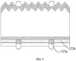
- step 104 referring to FIG. 8 , at least one first electrode 214 (also referred to as a front electrode 214) and at least one second electrode 228 (also referred to as a back electrode 228) are formed.
- either the at least one first electrode 214 or the at least one second electrode 218 serves as a hybrid electrode including a silver electrode, a conductive adhesive and an electrode film sequentially disposed in a direction away from the substrate.
- the second electrode 228 includes a silver electrode 228a, a conductive adhesive 228b, and an electrode film 228c that are sequentially disposed.
- the first electrode 214 has the same stacked structure as the second electrode 228.
- a structure of the first electrode is different from a structure of the second electrode.
- the process steps for forming the second electrode 228 are specifically as below.
- a thin layer of a silver paste is printed on a surface of the second passivation film 227 away from the substrate 20 by a screen printing process, and the silver paste is dried and sintered to form the silver electrode 228a that penetrates through the second passivation film 227 and contacts the first field passivation sub-layer 226a.
- the conductive adhesive 228b is laid on the silver electrode 228a.
- the electrode film 228c is laid on a surface of the conductive adhesive 228b. At last, an adhesive connection between the silver electrode 228a and the electrode film 228c is realized by the conductive adhesive 228b under a preset temperature and pressure condition.
- the silver electrode 228a is prepared by printing and sintering the silver paste, which is mainly to ensure that a good tensile force may be formed between the second electrode 228 and the field passivation layer 226.
- the silver electrode 228a includes one of a plurality of sub-gate lines or a main gate line connecting the plurality of sub-gate lines.
- An extending direction of the main gate line is generally perpendicular to an extending direction of the sub-gate lines, and the main gate line is used for a connection between the solar cells in the subsequent preparing process of a module.
- the conductive adhesive 228b may cover the main gate line or a plurality of sub-gate lines. Taking the main gate line as an example, when the conductive adhesive 228b covers the main gate line, in a direction perpendicular to the extending direction of the main gate line, a width of the conductive adhesive 228b is 1% ⁇ 100% of a width of the silver electrode 228a.
- the conductive adhesive 228b may be a continuous coverage or a discontinuous coverage, preferably with a width ratio of 100% and the continuous coverage. In the extending direction of the main gate line, a length of the conductive adhesive 228b is 50% ⁇ 100% of a length of the main gate line.
- the conductive adhesive 228b may be the continuous coverage or the discontinuous coverage, preferably with a length ratio of 100% and the continuous coverage.
- the conductive adhesive 228b is an adhesive with a certain conductive property after curing or drying, which includes a base and conductive particles.
- the base has a bonding effect to bond the conductive particles together to form a conductive path and realize a conductive connection of bonded materials.
- the base is made of an acrylic acid, an epoxy, a silica gel, a maleic anhydride or a hybrid resin, and the conductive particles are made of a silver, a silver-coated copper, a gold, a nickel or a carbon.
- the electrode film 228c may be fully or partially disposed on the conductive adhesive 228b.
- the electrode film 228c can be made of a conductive organic compound, a conductive inorganic compound, a non-silver metal, a non-silver metal composite, or the like, or any combination thereof.
- the conductive inorganic compound includes a carbon.
- the non-silver metal includes a gold, a nickel, a copper, a tin, an aluminum, etc.
- a height of the electrode film 228c may be adjusted according to actual needs in order to increase a cross-sectional area of a current transmission, reduce a transmission resistance of the second electrode 228, and improve the conversion efficiency of the solar cell.
- the material of the bonded electrode film 228c is not limited, a material with a relatively low cost may be selected to reduce a producing cost of the solar cell.
- the first field passivation sub-layer in contact with the second electrode has a relatively high conductivity, which is conducive to ensuring the effective transmission of the majority carriers and improving the short-circuit current of the solar cell.
- the thickness of the second field passivation sub-layer is smaller than the thickness of the first field passivation sub-layer, which is conductive to weakening the light absorption capability of the second field passivation sub-layer, thus improving the conversion efficiency of the solar cell.
- the electrode film bonded by the conductive adhesive may be any conductive material, that is, may be a material with the lower cost than the silver, which is conductive to reducing the cost of the solar cell.
- an embodiment of the present disclosure further provides a solar cell which may be produced by the above-described method for producing the solar cell.
- the solar cell includes: a substrate 20; a first passivation film 212, an anti-reflection layer 213 and a first electrode 214 sequentially disposed on a front surface of the substrate 20; and a tunneling layer 221, a field passivation layer 226 and a second electrode 228 sequentially disposed on a rear surface of the substrate 20.
- the field passivation layer 226 includes a first field passivation sub-layer 226a corresponding to a portion of the field passivation layer 226 between the second electrode 228 and the substrate 20 and a second field passivation sub-layer 226b corresponding to a portion of the field passivation layer 226 between adjacent second electrodes 228.
- a conductivity of the first field passivation sub-layer 226a is greater than a conductivity of the second field passivation sub-layer 226b, and a thickness of the second field passivation sub-layer 226b is smaller than a thickness of the first field passivation sub-layer 226a in a direction perpendicular to a surface of the substrate 20.
- the first electrode 214 includes a silver electrode, a conductive adhesive, and an electrode film that are sequentially formed; and/or, in a direction away from the substrate 20 toward the field passivation layer 226, the second electrode 228 includes a silver electrode 228a, a conductive adhesive 228b, and an electrode film 228c that are sequentially disposed.
- a bottom surface of the second field passivation sub-layer 226b is flush with a bottom surface of the first field passivation sub-layer 226a in the direction away from the substrate 20 toward the field passivation layer 226.
- a thickness difference between the second field passivation sub-layer 226b and the first field passivation sub-layer 226a is 50 nm ⁇ 80 nm, for example, 60 nm, 65 nm or 70 nm.
- a material of the first field passivation sub-layer 322a is different from a material of the second field passivation sub-layer 322b. Specifically, an absorption coefficient of the material of the second field passivation sub-layer 322b is smaller than an absorption coefficient of the material of the first field passivation sub-layer 322a.
- the material of the first field passivation sub-layer 322a is a polycrystalline silicon
- the material of the second field passivation sub-layer 322b is an amorphous silicon. Since a passivated contact structure is adopted for a back surface of the solar cell, and a sunlight is mainly in a long-wave spectrum after reaching the back surface, using the amorphous silicon with a relatively low absorption coefficient in the long-wave spectrum as the material of the second field passivation sub-layer 322b may reduce an absorption in the long-wave spectrum and improve a conversion efficiency of the solar cell.
- a surface doping concentration of a top surface of the second field passivation sub-layer 226b is lower than a surface doping concentration of a top surface of the first field passivation sub-layer 226a.
- a surface doping concentration difference between the top surface of the first field passivation sub-layer 226a and the top surface of the second field passivation sub-layer 226b is 0.5E+20/cm 3 ⁇ 1.5E+20/cm 3 , for example, 0.75 E+20/cm 3 , 1 E+20/cm 3 or 1.25 E+20/cm 3 .
- the first field passivation sub-layer 226a in the direction away from the substrate 20, includes an ion diffusion layer 223 and an ion enrichment layer 224 that are sequentially formed, and a doping concentration of the ion enrichment layer 224 is greater than a doping concentration of the ion diffusion layer 223.
- the top surface of the second field passivation sub-layer 226b is lower than the top surface of the first field passivation sub-layer 226a, and a thickness difference between the second field passivation sub-layer 226b and the first field passivation sub-layer 226a is greater than a thickness of the ion enrichment layer 224.
- the silver electrode 228a includes a plurality of sub-gate lines or a main gate line connecting the plurality of sub-gate lines.
- the conductive adhesive 228b covers one or more of the main gate line and the plurality of sub-gate lines.
- the electrode film 228c is made of a conductive organic compound, a conductive inorganic compound, a non-silver metal or a non-silver metal composite, and the non-silver metal includes a gold, a nickel, a copper, a tin or an aluminum, etc.
- the conductive adhesive 228b includes a base and conductive particles.
- the base is made of an acrylic acid, an epoxy, a silica gel, a maleic anhydride or a hybrid resin, and the conductive particles are made of a silver, a silver-coated copper, a gold, a nickel or a carbon.
- a thickness of the silver electrode 228a may be 1 ⁇ 5 ⁇ m
- a thickness of the first passivation film 212 and a second passivation film 227 may be 0 ⁇ 100 nm
- a thickness of the conductive adhesive 228b may be 1 ⁇ 5 ⁇ m
- a thickness of the electrode film 228c may be 5 ⁇ 20 ⁇ m.
- the first field passivation sub-layer in contact with the second electrode has a relatively high conductivity, which is conducive to ensuring an effective transmission of majority carriers and improving a short-circuit current of the solar cell.
- the thickness of the second field passivation sub-layer is smaller than the thickness of the first field passivation sub-layer, which is conductive to weakening a light absorption capability of the second field passivation sub-layer, thus improving the conversion efficiency of the solar cell.
- the electrode film bonded by the conductive adhesive may be any conductive material, that is, may be a material with a lower cost than the silver, which is conductive to reducing the cost of the solar cell.
Landscapes
- Photovoltaic Devices (AREA)
- Life Sciences & Earth Sciences (AREA)
- Sustainable Development (AREA)
- Engineering & Computer Science (AREA)
- Sustainable Energy (AREA)
Priority Applications (2)
| Application Number | Priority Date | Filing Date | Title |
|---|---|---|---|
| EP23178062.8A EP4235816B1 (de) | 2020-11-19 | 2020-12-22 | Solarzelle und verfahren zur herstellung davon |
| EP22188010.7A EP4099400B1 (de) | 2020-11-19 | 2020-12-22 | Solarzelle und verfahren zur herstellung davon |
Applications Claiming Priority (1)
| Application Number | Priority Date | Filing Date | Title |
|---|---|---|---|
| CN202011307502.0A CN112466961B (zh) | 2020-11-19 | 2020-11-19 | 太阳能电池及其制造方法 |
Related Child Applications (3)
| Application Number | Title | Priority Date | Filing Date |
|---|---|---|---|
| EP22188010.7A Division EP4099400B1 (de) | 2020-11-19 | 2020-12-22 | Solarzelle und verfahren zur herstellung davon |
| EP22188010.7A Division-Into EP4099400B1 (de) | 2020-11-19 | 2020-12-22 | Solarzelle und verfahren zur herstellung davon |
| EP23178062.8A Division EP4235816B1 (de) | 2020-11-19 | 2020-12-22 | Solarzelle und verfahren zur herstellung davon |
Publications (2)
| Publication Number | Publication Date |
|---|---|
| EP4002487A1 true EP4002487A1 (de) | 2022-05-25 |
| EP4002487B1 EP4002487B1 (de) | 2022-09-28 |
Family
ID=73856731
Family Applications (3)
| Application Number | Title | Priority Date | Filing Date |
|---|---|---|---|
| EP22188010.7A Active EP4099400B1 (de) | 2020-11-19 | 2020-12-22 | Solarzelle und verfahren zur herstellung davon |
| EP20216350.7A Active EP4002487B1 (de) | 2020-11-19 | 2020-12-22 | Solarzelle und verfahren zur herstellung davon |
| EP23178062.8A Active EP4235816B1 (de) | 2020-11-19 | 2020-12-22 | Solarzelle und verfahren zur herstellung davon |
Family Applications Before (1)
| Application Number | Title | Priority Date | Filing Date |
|---|---|---|---|
| EP22188010.7A Active EP4099400B1 (de) | 2020-11-19 | 2020-12-22 | Solarzelle und verfahren zur herstellung davon |
Family Applications After (1)
| Application Number | Title | Priority Date | Filing Date |
|---|---|---|---|
| EP23178062.8A Active EP4235816B1 (de) | 2020-11-19 | 2020-12-22 | Solarzelle und verfahren zur herstellung davon |
Country Status (5)
| Country | Link |
|---|---|
| US (2) | US11450775B2 (de) |
| EP (3) | EP4099400B1 (de) |
| JP (1) | JP6970271B1 (de) |
| CN (1) | CN112466961B (de) |
| AU (3) | AU2020294222B1 (de) |
Cited By (2)
| Publication number | Priority date | Publication date | Assignee | Title |
|---|---|---|---|---|
| EP4300600A1 (de) * | 2022-06-30 | 2024-01-03 | Zhejiang Jinko Solar Co., Ltd. | Fotovoltaische zelle, verfahren zur herstellung davon und fotovoltaisches modul |
| US12100771B1 (en) | 2023-04-21 | 2024-09-24 | Jinko Solar (Haining) Co., Ltd. | Solar cell, method for preparing solar cell, and photovoltaic module |
Families Citing this family (15)
| Publication number | Priority date | Publication date | Assignee | Title |
|---|---|---|---|---|
| CN109390206A (zh) * | 2017-08-04 | 2019-02-26 | 中国科学技术大学 | 小型化便携式质谱仪及用于产生水团簇离子的离子源装置 |
| CN115274868B (zh) * | 2021-04-29 | 2023-07-21 | 浙江晶科能源有限公司 | 太阳能电池及光伏组件 |
| CN114420773B (zh) * | 2022-02-24 | 2024-07-02 | 天合光能股份有限公司 | 太阳能电池片、电池串及二者的制备方法 |
| EP4287267B1 (de) * | 2022-06-01 | 2024-12-25 | Jinko Solar (Haining) Co., Ltd. | Fotovoltaikzelle und fotovoltaikmodul |
| CN116722055A (zh) * | 2022-06-27 | 2023-09-08 | 浙江晶科能源有限公司 | 一种太阳能电池及光伏组件 |
| AU2022241631B1 (en) | 2022-08-05 | 2024-01-04 | Jinko Solar Co., Ltd. | Solar cell and photovoltaic module |
| CN116895703A (zh) * | 2022-08-05 | 2023-10-17 | 浙江晶科能源有限公司 | 太阳能电池及光伏组件 |
| CN116722060A (zh) | 2022-09-28 | 2023-09-08 | 浙江晶科能源有限公司 | 太阳能电池及光伏组件 |
| CN118156325A (zh) * | 2022-12-07 | 2024-06-07 | 浙江晶科能源有限公司 | 太阳能电池及光伏组件 |
| CN115881835B (zh) | 2023-02-08 | 2024-05-14 | 浙江晶科能源有限公司 | 太阳能电池及其制备方法、光伏组件 |
| CN115985981B (zh) | 2023-02-22 | 2023-06-20 | 浙江晶科能源有限公司 | 太阳能电池及其制备方法、光伏组件 |
| CN118099229A (zh) * | 2023-10-08 | 2024-05-28 | 晶科能源(海宁)有限公司 | 太阳能电池、光伏组件 |
| CN119008720A (zh) * | 2023-12-26 | 2024-11-22 | 浙江晶科能源有限公司 | 太阳能电池及其制备方法、光伏组件 |
| CN118448490B (zh) * | 2024-04-28 | 2025-10-21 | 隆基绿能科技股份有限公司 | 一种太阳能电池及其制备方法和光伏组件 |
| CN118180357B (zh) * | 2024-05-16 | 2024-07-26 | 广州众山紧固件有限公司 | 一种铜铝复合金属板及铸造成型方法和其在散热器中的应用 |
Citations (3)
| Publication number | Priority date | Publication date | Assignee | Title |
|---|---|---|---|---|
| EP3026713A1 (de) * | 2014-11-28 | 2016-06-01 | LG Electronics Inc. | Solarzelle und verfahren zur herstellung davon |
| KR20160063861A (ko) * | 2014-11-27 | 2016-06-07 | 엘지전자 주식회사 | 태양 전지 |
| CN106449800B (zh) * | 2016-12-07 | 2019-04-05 | 天合光能股份有限公司 | 选择性多晶硅薄膜的钝化接触结构及其制备方法 |
Family Cites Families (30)
| Publication number | Priority date | Publication date | Assignee | Title |
|---|---|---|---|---|
| US20070169808A1 (en) * | 2006-01-26 | 2007-07-26 | Kherani Nazir P | Solar cell |
| US20100032012A1 (en) | 2006-12-01 | 2010-02-11 | Takayuki Isaka | Solar cell and method of manufacturing the same |
| JP2009231813A (ja) | 2008-02-27 | 2009-10-08 | Sanyo Electric Co Ltd | 太陽電池モジュール及びその製造方法 |
| JP5171653B2 (ja) * | 2009-01-07 | 2013-03-27 | 三菱電機株式会社 | 太陽電池とその製造方法 |
| WO2011035090A1 (en) | 2009-09-17 | 2011-03-24 | Tetrasun, Inc. | Selective transformation in functional films, and solar cell applications thereof |
| KR20120082664A (ko) * | 2011-01-14 | 2012-07-24 | 엘지전자 주식회사 | 태양 전지의 제조 방법 |
| JP5840418B2 (ja) | 2011-08-23 | 2016-01-06 | デクセリアルズ株式会社 | 導電性接着剤及び太陽電池モジュール |
| WO2013148047A1 (en) * | 2012-03-30 | 2013-10-03 | Applied Materials, Inc. | Doped ai paste for local alloyed junction formation with low contact resistance |
| CN203038932U (zh) * | 2012-11-20 | 2013-07-03 | 上饶光电高科技有限公司 | 一种背发射极太阳能电池 |
| KR101613843B1 (ko) * | 2013-04-23 | 2016-04-20 | 엘지전자 주식회사 | 태양 전지 및 이의 제조 방법 |
| NL2010941C2 (en) * | 2013-06-07 | 2014-12-09 | Stichting Energie | Photovoltaic cell and method for manufacturing such a photovoltaic cell. |
| KR102132740B1 (ko) | 2013-10-21 | 2020-07-10 | 엘지전자 주식회사 | 태양 전지 및 이의 제조 방법 |
| JP5735093B1 (ja) | 2013-12-24 | 2015-06-17 | 株式会社マテリアル・コンセプト | 太陽電池及びその製造方法 |
| WO2016011426A1 (en) * | 2014-07-17 | 2016-01-21 | Solarcity Corporation | Solar cell with interdigitated back contact |
| KR101661807B1 (ko) * | 2014-07-28 | 2016-09-30 | 엘지전자 주식회사 | 태양 전지 및 그 제조 방법 |
| CN204011456U (zh) * | 2014-09-05 | 2014-12-10 | 浙江晶科能源有限公司 | 一种具有全背面铝导电反射器的晶体硅太阳电池 |
| CN105762202B (zh) | 2016-04-28 | 2017-08-15 | 泰州乐叶光伏科技有限公司 | 一种点线结合的太阳能电池正面电极及其制备方法 |
| CN105789345B (zh) | 2016-04-28 | 2018-03-09 | 泰州隆基乐叶光伏科技有限公司 | 一种太阳能电池的正面电极结构及其制备方法 |
| CN105702759B (zh) * | 2016-04-28 | 2018-03-09 | 泰州隆基乐叶光伏科技有限公司 | 一种太阳能电池主栅电极结构及其制备方法 |
| US10686087B2 (en) | 2016-09-19 | 2020-06-16 | Lg Electronics Inc. | Solar cell and method for manufacturing the same |
| US20180138337A1 (en) * | 2016-11-15 | 2018-05-17 | Alliance For Sustainable Energy, Llc | Transparent Conductive Adhesive Materials |
| CN206225372U (zh) | 2016-12-07 | 2017-06-06 | 常州天合光能有限公司 | 选择性多晶硅薄膜的钝化接触结构 |
| JPWO2019021545A1 (ja) * | 2017-07-28 | 2019-11-07 | 三菱電機株式会社 | 太陽電池、及び、その製造方法 |
| TWI662715B (zh) * | 2017-10-27 | 2019-06-11 | 財團法人工業技術研究院 | 太陽能電池 |
| CN109494261B (zh) * | 2018-10-19 | 2024-06-21 | 晶澳(扬州)太阳能科技有限公司 | 硅基太阳能电池及制备方法、光伏组件 |
| CN110265494A (zh) | 2019-07-12 | 2019-09-20 | 苏州中来光伏新材股份有限公司 | 一种局部背场TOPCon太阳能电池及其制备方法 |
| CN110571299B (zh) * | 2019-08-29 | 2021-10-01 | 东方日升(常州)新能源有限公司 | 一种自对准式埋栅钝化接触晶硅太阳电池及其制备方法 |
| CN110838528B (zh) * | 2019-10-29 | 2021-07-06 | 协鑫集成科技股份有限公司 | 一种后掺杂式n型接触钝化电池 |
| CN210897294U (zh) * | 2019-10-29 | 2020-06-30 | 苏州阿特斯阳光电力科技有限公司 | 太阳能电池 |
| CN111628050B (zh) * | 2020-06-11 | 2021-08-03 | 常州时创能源股份有限公司 | 实现电子局部钝化接触的方法、晶体硅太阳能电池及其制备方法 |
-
2020
- 2020-11-19 CN CN202011307502.0A patent/CN112466961B/zh active Active
- 2020-12-22 JP JP2020212129A patent/JP6970271B1/ja active Active
- 2020-12-22 EP EP22188010.7A patent/EP4099400B1/de active Active
- 2020-12-22 EP EP20216350.7A patent/EP4002487B1/de active Active
- 2020-12-22 EP EP23178062.8A patent/EP4235816B1/de active Active
- 2020-12-23 US US17/133,560 patent/US11450775B2/en active Active
- 2020-12-23 AU AU2020294222A patent/AU2020294222B1/en active Active
-
2022
- 2022-04-04 AU AU2022202235A patent/AU2022202235B2/en active Active
- 2022-08-02 US US17/878,914 patent/US11990554B2/en active Active
-
2023
- 2023-06-09 AU AU2023203634A patent/AU2023203634B2/en active Active
Patent Citations (3)
| Publication number | Priority date | Publication date | Assignee | Title |
|---|---|---|---|---|
| KR20160063861A (ko) * | 2014-11-27 | 2016-06-07 | 엘지전자 주식회사 | 태양 전지 |
| EP3026713A1 (de) * | 2014-11-28 | 2016-06-01 | LG Electronics Inc. | Solarzelle und verfahren zur herstellung davon |
| CN106449800B (zh) * | 2016-12-07 | 2019-04-05 | 天合光能股份有限公司 | 选择性多晶硅薄膜的钝化接触结构及其制备方法 |
Cited By (4)
| Publication number | Priority date | Publication date | Assignee | Title |
|---|---|---|---|---|
| EP4300600A1 (de) * | 2022-06-30 | 2024-01-03 | Zhejiang Jinko Solar Co., Ltd. | Fotovoltaische zelle, verfahren zur herstellung davon und fotovoltaisches modul |
| US11967656B2 (en) | 2022-06-30 | 2024-04-23 | Zhejiang Jinko Solar Co., Ltd. | Photovoltaic cell, method for preparing same, and photovoltaic module |
| US12100771B1 (en) | 2023-04-21 | 2024-09-24 | Jinko Solar (Haining) Co., Ltd. | Solar cell, method for preparing solar cell, and photovoltaic module |
| EP4451350A1 (de) * | 2023-04-21 | 2024-10-23 | Jinko Solar (Haining) Co., Ltd. | Solarzelle, verfahren zur herstellung einer solarzelle und fotovoltaisches modul |
Also Published As
| Publication number | Publication date |
|---|---|
| EP4235816A3 (de) | 2023-10-25 |
| JP2022081367A (ja) | 2022-05-31 |
| CN112466961A (zh) | 2021-03-09 |
| US20220376122A1 (en) | 2022-11-24 |
| AU2023203634A1 (en) | 2023-07-06 |
| EP4099400A1 (de) | 2022-12-07 |
| EP4099400C0 (de) | 2023-09-06 |
| US20220158003A1 (en) | 2022-05-19 |
| US11990554B2 (en) | 2024-05-21 |
| AU2023203634B2 (en) | 2025-02-27 |
| AU2022202235A1 (en) | 2022-04-21 |
| US11450775B2 (en) | 2022-09-20 |
| EP4235816C0 (de) | 2024-11-06 |
| AU2020294222B1 (en) | 2022-03-10 |
| JP6970271B1 (ja) | 2021-11-24 |
| EP4099400B1 (de) | 2023-09-06 |
| EP4235816B1 (de) | 2024-11-06 |
| EP4235816A2 (de) | 2023-08-30 |
| EP4002487B1 (de) | 2022-09-28 |
| CN112466961B (zh) | 2024-05-10 |
| AU2022202235B2 (en) | 2023-05-18 |
Similar Documents
| Publication | Publication Date | Title |
|---|---|---|
| EP4002487B1 (de) | Solarzelle und verfahren zur herstellung davon | |
| CN115241298B (zh) | 太阳能电池及其制备方法、光伏组件 | |
| CN112349798B (zh) | 太阳能电池及其制造方法 | |
| NL2033695B1 (en) | Solar cell and production method thereof, photovoltaic module | |
| EP2650926B1 (de) | Solarzelle und verfahren zur herstellung einer solarzelle | |
| CN113707761A (zh) | 一种n型选择性发射极太阳能电池及其制备方法 | |
| CN115732576A (zh) | 太阳能电池及其形成方法、光伏组件 | |
| EP4300600B1 (de) | Fotovoltaische zelle, verfahren zur herstellung davon und fotovoltaisches modul | |
| JP2025096191A (ja) | 太陽電池及びその製造方法、光起電力モジュール | |
| JP7796804B2 (ja) | 太陽電池及びその製造方法、光起電力モジュール | |
| EP4626181A1 (de) | Solarzelle und herstellungsverfahren für die solarzelle | |
| CN217933805U (zh) | 太阳能电池及光伏组件 | |
| CN117727807B (zh) | 异质结太阳能电池及其制备方法和光伏组件 | |
| CN115132858B (zh) | 太阳能电池生产方法及太阳能电池 | |
| CN218730968U (zh) | 太阳能电池及光伏组件 | |
| CN114744064B (zh) | 太阳能电池及生产方法、光伏组件 | |
| CN117423757A (zh) | 一种太阳能电池以及光伏组件 |
Legal Events
| Date | Code | Title | Description |
|---|---|---|---|
| PUAI | Public reference made under article 153(3) epc to a published international application that has entered the european phase |
Free format text: ORIGINAL CODE: 0009012 |
|
| STAA | Information on the status of an ep patent application or granted ep patent |
Free format text: STATUS: REQUEST FOR EXAMINATION WAS MADE |
|
| 17P | Request for examination filed |
Effective date: 20201223 |
|
| AK | Designated contracting states |
Kind code of ref document: A1 Designated state(s): AL AT BE BG CH CY CZ DE DK EE ES FI FR GB GR HR HU IE IS IT LI LT LU LV MC MK MT NL NO PL PT RO RS SE SI SK SM TR |
|
| GRAP | Despatch of communication of intention to grant a patent |
Free format text: ORIGINAL CODE: EPIDOSNIGR1 |
|
| STAA | Information on the status of an ep patent application or granted ep patent |
Free format text: STATUS: GRANT OF PATENT IS INTENDED |
|
| INTG | Intention to grant announced |
Effective date: 20220715 |
|
| GRAS | Grant fee paid |
Free format text: ORIGINAL CODE: EPIDOSNIGR3 |
|
| GRAA | (expected) grant |
Free format text: ORIGINAL CODE: 0009210 |
|
| STAA | Information on the status of an ep patent application or granted ep patent |
Free format text: STATUS: THE PATENT HAS BEEN GRANTED |
|
| AK | Designated contracting states |
Kind code of ref document: B1 Designated state(s): AL AT BE BG CH CY CZ DE DK EE ES FI FR GB GR HR HU IE IS IT LI LT LU LV MC MK MT NL NO PL PT RO RS SE SI SK SM TR |
|
| REG | Reference to a national code |
Ref country code: GB Ref legal event code: FG4D |
|
| REG | Reference to a national code |
Ref country code: CH Ref legal event code: EP |
|
| REG | Reference to a national code |
Ref country code: AT Ref legal event code: REF Ref document number: 1521817 Country of ref document: AT Kind code of ref document: T Effective date: 20221015 |
|
| REG | Reference to a national code |
Ref country code: DE Ref legal event code: R096 Ref document number: 602020005368 Country of ref document: DE |
|
| REG | Reference to a national code |
Ref country code: IE Ref legal event code: FG4D |
|
| REG | Reference to a national code |
Ref country code: NL Ref legal event code: FP |
|
| REG | Reference to a national code |
Ref country code: LT Ref legal event code: MG9D |
|
| PG25 | Lapsed in a contracting state [announced via postgrant information from national office to epo] |
Ref country code: SE Free format text: LAPSE BECAUSE OF FAILURE TO SUBMIT A TRANSLATION OF THE DESCRIPTION OR TO PAY THE FEE WITHIN THE PRESCRIBED TIME-LIMIT Effective date: 20220928 Ref country code: RS Free format text: LAPSE BECAUSE OF FAILURE TO SUBMIT A TRANSLATION OF THE DESCRIPTION OR TO PAY THE FEE WITHIN THE PRESCRIBED TIME-LIMIT Effective date: 20220928 Ref country code: NO Free format text: LAPSE BECAUSE OF FAILURE TO SUBMIT A TRANSLATION OF THE DESCRIPTION OR TO PAY THE FEE WITHIN THE PRESCRIBED TIME-LIMIT Effective date: 20221228 Ref country code: LV Free format text: LAPSE BECAUSE OF FAILURE TO SUBMIT A TRANSLATION OF THE DESCRIPTION OR TO PAY THE FEE WITHIN THE PRESCRIBED TIME-LIMIT Effective date: 20220928 Ref country code: LT Free format text: LAPSE BECAUSE OF FAILURE TO SUBMIT A TRANSLATION OF THE DESCRIPTION OR TO PAY THE FEE WITHIN THE PRESCRIBED TIME-LIMIT Effective date: 20220928 Ref country code: FI Free format text: LAPSE BECAUSE OF FAILURE TO SUBMIT A TRANSLATION OF THE DESCRIPTION OR TO PAY THE FEE WITHIN THE PRESCRIBED TIME-LIMIT Effective date: 20220928 |
|
| REG | Reference to a national code |
Ref country code: AT Ref legal event code: MK05 Ref document number: 1521817 Country of ref document: AT Kind code of ref document: T Effective date: 20220928 |
|
| PG25 | Lapsed in a contracting state [announced via postgrant information from national office to epo] |
Ref country code: HR Free format text: LAPSE BECAUSE OF FAILURE TO SUBMIT A TRANSLATION OF THE DESCRIPTION OR TO PAY THE FEE WITHIN THE PRESCRIBED TIME-LIMIT Effective date: 20220928 Ref country code: GR Free format text: LAPSE BECAUSE OF FAILURE TO SUBMIT A TRANSLATION OF THE DESCRIPTION OR TO PAY THE FEE WITHIN THE PRESCRIBED TIME-LIMIT Effective date: 20221229 |
|
| PG25 | Lapsed in a contracting state [announced via postgrant information from national office to epo] |
Ref country code: SM Free format text: LAPSE BECAUSE OF FAILURE TO SUBMIT A TRANSLATION OF THE DESCRIPTION OR TO PAY THE FEE WITHIN THE PRESCRIBED TIME-LIMIT Effective date: 20220928 Ref country code: RO Free format text: LAPSE BECAUSE OF FAILURE TO SUBMIT A TRANSLATION OF THE DESCRIPTION OR TO PAY THE FEE WITHIN THE PRESCRIBED TIME-LIMIT Effective date: 20220928 Ref country code: PT Free format text: LAPSE BECAUSE OF FAILURE TO SUBMIT A TRANSLATION OF THE DESCRIPTION OR TO PAY THE FEE WITHIN THE PRESCRIBED TIME-LIMIT Effective date: 20230130 Ref country code: ES Free format text: LAPSE BECAUSE OF FAILURE TO SUBMIT A TRANSLATION OF THE DESCRIPTION OR TO PAY THE FEE WITHIN THE PRESCRIBED TIME-LIMIT Effective date: 20220928 Ref country code: CZ Free format text: LAPSE BECAUSE OF FAILURE TO SUBMIT A TRANSLATION OF THE DESCRIPTION OR TO PAY THE FEE WITHIN THE PRESCRIBED TIME-LIMIT Effective date: 20220928 Ref country code: AT Free format text: LAPSE BECAUSE OF FAILURE TO SUBMIT A TRANSLATION OF THE DESCRIPTION OR TO PAY THE FEE WITHIN THE PRESCRIBED TIME-LIMIT Effective date: 20220928 |
|
| PG25 | Lapsed in a contracting state [announced via postgrant information from national office to epo] |
Ref country code: SK Free format text: LAPSE BECAUSE OF FAILURE TO SUBMIT A TRANSLATION OF THE DESCRIPTION OR TO PAY THE FEE WITHIN THE PRESCRIBED TIME-LIMIT Effective date: 20220928 Ref country code: PL Free format text: LAPSE BECAUSE OF FAILURE TO SUBMIT A TRANSLATION OF THE DESCRIPTION OR TO PAY THE FEE WITHIN THE PRESCRIBED TIME-LIMIT Effective date: 20220928 Ref country code: IS Free format text: LAPSE BECAUSE OF FAILURE TO SUBMIT A TRANSLATION OF THE DESCRIPTION OR TO PAY THE FEE WITHIN THE PRESCRIBED TIME-LIMIT Effective date: 20230128 Ref country code: EE Free format text: LAPSE BECAUSE OF FAILURE TO SUBMIT A TRANSLATION OF THE DESCRIPTION OR TO PAY THE FEE WITHIN THE PRESCRIBED TIME-LIMIT Effective date: 20220928 |
|
| P01 | Opt-out of the competence of the unified patent court (upc) registered |
Effective date: 20230507 |
|
| REG | Reference to a national code |
Ref country code: DE Ref legal event code: R097 Ref document number: 602020005368 Country of ref document: DE |
|
| PG25 | Lapsed in a contracting state [announced via postgrant information from national office to epo] |
Ref country code: AL Free format text: LAPSE BECAUSE OF FAILURE TO SUBMIT A TRANSLATION OF THE DESCRIPTION OR TO PAY THE FEE WITHIN THE PRESCRIBED TIME-LIMIT Effective date: 20220928 |
|
| PG25 | Lapsed in a contracting state [announced via postgrant information from national office to epo] |
Ref country code: DK Free format text: LAPSE BECAUSE OF FAILURE TO SUBMIT A TRANSLATION OF THE DESCRIPTION OR TO PAY THE FEE WITHIN THE PRESCRIBED TIME-LIMIT Effective date: 20220928 |
|
| PLBE | No opposition filed within time limit |
Free format text: ORIGINAL CODE: 0009261 |
|
| STAA | Information on the status of an ep patent application or granted ep patent |
Free format text: STATUS: NO OPPOSITION FILED WITHIN TIME LIMIT |
|
| REG | Reference to a national code |
Ref country code: BE Ref legal event code: MM Effective date: 20221231 |
|
| PG25 | Lapsed in a contracting state [announced via postgrant information from national office to epo] |
Ref country code: LU Free format text: LAPSE BECAUSE OF NON-PAYMENT OF DUE FEES Effective date: 20221222 |
|
| 26N | No opposition filed |
Effective date: 20230629 |
|
| PG25 | Lapsed in a contracting state [announced via postgrant information from national office to epo] |
Ref country code: IE Free format text: LAPSE BECAUSE OF NON-PAYMENT OF DUE FEES Effective date: 20221222 |
|
| PG25 | Lapsed in a contracting state [announced via postgrant information from national office to epo] |
Ref country code: SI Free format text: LAPSE BECAUSE OF FAILURE TO SUBMIT A TRANSLATION OF THE DESCRIPTION OR TO PAY THE FEE WITHIN THE PRESCRIBED TIME-LIMIT Effective date: 20220928 Ref country code: BE Free format text: LAPSE BECAUSE OF NON-PAYMENT OF DUE FEES Effective date: 20221231 |
|
| PG25 | Lapsed in a contracting state [announced via postgrant information from national office to epo] |
Ref country code: CY Free format text: LAPSE BECAUSE OF FAILURE TO SUBMIT A TRANSLATION OF THE DESCRIPTION OR TO PAY THE FEE WITHIN THE PRESCRIBED TIME-LIMIT Effective date: 20220928 |
|
| PG25 | Lapsed in a contracting state [announced via postgrant information from national office to epo] |
Ref country code: MK Free format text: LAPSE BECAUSE OF FAILURE TO SUBMIT A TRANSLATION OF THE DESCRIPTION OR TO PAY THE FEE WITHIN THE PRESCRIBED TIME-LIMIT Effective date: 20220928 |
|
| PG25 | Lapsed in a contracting state [announced via postgrant information from national office to epo] |
Ref country code: MC Free format text: LAPSE BECAUSE OF FAILURE TO SUBMIT A TRANSLATION OF THE DESCRIPTION OR TO PAY THE FEE WITHIN THE PRESCRIBED TIME-LIMIT Effective date: 20220928 |
|
| PG25 | Lapsed in a contracting state [announced via postgrant information from national office to epo] |
Ref country code: MC Free format text: LAPSE BECAUSE OF FAILURE TO SUBMIT A TRANSLATION OF THE DESCRIPTION OR TO PAY THE FEE WITHIN THE PRESCRIBED TIME-LIMIT Effective date: 20220928 |
|
| PG25 | Lapsed in a contracting state [announced via postgrant information from national office to epo] |
Ref country code: BG Free format text: LAPSE BECAUSE OF FAILURE TO SUBMIT A TRANSLATION OF THE DESCRIPTION OR TO PAY THE FEE WITHIN THE PRESCRIBED TIME-LIMIT Effective date: 20220928 |
|
| REG | Reference to a national code |
Ref country code: CH Ref legal event code: PL |
|
| PG25 | Lapsed in a contracting state [announced via postgrant information from national office to epo] |
Ref country code: MT Free format text: LAPSE BECAUSE OF FAILURE TO SUBMIT A TRANSLATION OF THE DESCRIPTION OR TO PAY THE FEE WITHIN THE PRESCRIBED TIME-LIMIT Effective date: 20220928 |
|
| PG25 | Lapsed in a contracting state [announced via postgrant information from national office to epo] |
Ref country code: CH Free format text: LAPSE BECAUSE OF NON-PAYMENT OF DUE FEES Effective date: 20231231 |
|
| PG25 | Lapsed in a contracting state [announced via postgrant information from national office to epo] |
Ref country code: CH Free format text: LAPSE BECAUSE OF NON-PAYMENT OF DUE FEES Effective date: 20231231 |
|
| REG | Reference to a national code |
Ref country code: DE Ref legal event code: R079 Ref document number: 602020005368 Country of ref document: DE Free format text: PREVIOUS MAIN CLASS: H01L0031021600 Ipc: H10F0077300000 |
|
| REG | Reference to a national code |
Ref country code: DE Ref legal event code: R081 Ref document number: 602020005368 Country of ref document: DE Owner name: JINKO SOLAR CO., LTD., CN Free format text: FORMER OWNERS: JINKO GREEN ENERGY (SHANGHAI) MANAGEMENT CO., LTD, SHANGHAI, CN; ZHEJIANG JINKO SOLAR CO., LTD., HAINING, ZHEJIANG, CN |
|
| REG | Reference to a national code |
Ref country code: NL Ref legal event code: PD Owner name: JINKO SOLAR CO., LTD.; CN Free format text: DETAILS ASSIGNMENT: CHANGE OF OWNER(S), ASSIGNMENT; FORMER OWNER NAME: ZHEJIANG JINKO SOLAR CO., LTD. Effective date: 20250627 |
|
| PG25 | Lapsed in a contracting state [announced via postgrant information from national office to epo] |
Ref country code: HU Free format text: LAPSE BECAUSE OF FAILURE TO SUBMIT A TRANSLATION OF THE DESCRIPTION OR TO PAY THE FEE WITHIN THE PRESCRIBED TIME-LIMIT; INVALID AB INITIO Effective date: 20201222 |
|
| PG25 | Lapsed in a contracting state [announced via postgrant information from national office to epo] |
Ref country code: TR Free format text: LAPSE BECAUSE OF FAILURE TO SUBMIT A TRANSLATION OF THE DESCRIPTION OR TO PAY THE FEE WITHIN THE PRESCRIBED TIME-LIMIT Effective date: 20220928 |
|
| PGFP | Annual fee paid to national office [announced via postgrant information from national office to epo] |
Ref country code: DE Payment date: 20251211 Year of fee payment: 6 |
|
| PGFP | Annual fee paid to national office [announced via postgrant information from national office to epo] |
Ref country code: GB Payment date: 20251219 Year of fee payment: 6 |
|
| PGFP | Annual fee paid to national office [announced via postgrant information from national office to epo] |
Ref country code: IT Payment date: 20251223 Year of fee payment: 6 |
|
| PGFP | Annual fee paid to national office [announced via postgrant information from national office to epo] |
Ref country code: NL Payment date: 20251219 Year of fee payment: 6 Ref country code: FR Payment date: 20251229 Year of fee payment: 6 |