EP4002495A2 - Solarzelle und herstellungsverfahren dafür - Google Patents
Solarzelle und herstellungsverfahren dafür Download PDFInfo
- Publication number
- EP4002495A2 EP4002495A2 EP20844936.3A EP20844936A EP4002495A2 EP 4002495 A2 EP4002495 A2 EP 4002495A2 EP 20844936 A EP20844936 A EP 20844936A EP 4002495 A2 EP4002495 A2 EP 4002495A2
- Authority
- EP
- European Patent Office
- Prior art keywords
- conductivity
- layer
- aluminum oxide
- type region
- forming
- Prior art date
- Legal status (The legal status is an assumption and is not a legal conclusion. Google has not performed a legal analysis and makes no representation as to the accuracy of the status listed.)
- Pending
Links
Images




Classifications
-
- H—ELECTRICITY
- H10—SEMICONDUCTOR DEVICES; ELECTRIC SOLID-STATE DEVICES NOT OTHERWISE PROVIDED FOR
- H10F—INORGANIC SEMICONDUCTOR DEVICES SENSITIVE TO INFRARED RADIATION, LIGHT, ELECTROMAGNETIC RADIATION OF SHORTER WAVELENGTH OR CORPUSCULAR RADIATION
- H10F77/00—Constructional details of devices covered by this subclass
- H10F77/30—Coatings
- H10F77/306—Coatings for devices having potential barriers
- H10F77/311—Coatings for devices having potential barriers for photovoltaic cells
-
- H—ELECTRICITY
- H10—SEMICONDUCTOR DEVICES; ELECTRIC SOLID-STATE DEVICES NOT OTHERWISE PROVIDED FOR
- H10F—INORGANIC SEMICONDUCTOR DEVICES SENSITIVE TO INFRARED RADIATION, LIGHT, ELECTROMAGNETIC RADIATION OF SHORTER WAVELENGTH OR CORPUSCULAR RADIATION
- H10F71/00—Manufacture or treatment of devices covered by this subclass
- H10F71/129—Passivating
-
- H—ELECTRICITY
- H10—SEMICONDUCTOR DEVICES; ELECTRIC SOLID-STATE DEVICES NOT OTHERWISE PROVIDED FOR
- H10F—INORGANIC SEMICONDUCTOR DEVICES SENSITIVE TO INFRARED RADIATION, LIGHT, ELECTROMAGNETIC RADIATION OF SHORTER WAVELENGTH OR CORPUSCULAR RADIATION
- H10F10/00—Individual photovoltaic cells, e.g. solar cells
- H10F10/10—Individual photovoltaic cells, e.g. solar cells having potential barriers
- H10F10/14—Photovoltaic cells having only PN homojunction potential barriers
-
- H—ELECTRICITY
- H10—SEMICONDUCTOR DEVICES; ELECTRIC SOLID-STATE DEVICES NOT OTHERWISE PROVIDED FOR
- H10F—INORGANIC SEMICONDUCTOR DEVICES SENSITIVE TO INFRARED RADIATION, LIGHT, ELECTROMAGNETIC RADIATION OF SHORTER WAVELENGTH OR CORPUSCULAR RADIATION
- H10F71/00—Manufacture or treatment of devices covered by this subclass
-
- H—ELECTRICITY
- H10—SEMICONDUCTOR DEVICES; ELECTRIC SOLID-STATE DEVICES NOT OTHERWISE PROVIDED FOR
- H10F—INORGANIC SEMICONDUCTOR DEVICES SENSITIVE TO INFRARED RADIATION, LIGHT, ELECTROMAGNETIC RADIATION OF SHORTER WAVELENGTH OR CORPUSCULAR RADIATION
- H10F71/00—Manufacture or treatment of devices covered by this subclass
- H10F71/121—The active layers comprising only Group IV materials
- H10F71/1221—The active layers comprising only Group IV materials comprising polycrystalline silicon
-
- H—ELECTRICITY
- H10—SEMICONDUCTOR DEVICES; ELECTRIC SOLID-STATE DEVICES NOT OTHERWISE PROVIDED FOR
- H10F—INORGANIC SEMICONDUCTOR DEVICES SENSITIVE TO INFRARED RADIATION, LIGHT, ELECTROMAGNETIC RADIATION OF SHORTER WAVELENGTH OR CORPUSCULAR RADIATION
- H10F71/00—Manufacture or treatment of devices covered by this subclass
- H10F71/128—Annealing
-
- H—ELECTRICITY
- H10—SEMICONDUCTOR DEVICES; ELECTRIC SOLID-STATE DEVICES NOT OTHERWISE PROVIDED FOR
- H10F—INORGANIC SEMICONDUCTOR DEVICES SENSITIVE TO INFRARED RADIATION, LIGHT, ELECTROMAGNETIC RADIATION OF SHORTER WAVELENGTH OR CORPUSCULAR RADIATION
- H10F77/00—Constructional details of devices covered by this subclass
- H10F77/10—Semiconductor bodies
- H10F77/12—Active materials
-
- H—ELECTRICITY
- H10—SEMICONDUCTOR DEVICES; ELECTRIC SOLID-STATE DEVICES NOT OTHERWISE PROVIDED FOR
- H10F—INORGANIC SEMICONDUCTOR DEVICES SENSITIVE TO INFRARED RADIATION, LIGHT, ELECTROMAGNETIC RADIATION OF SHORTER WAVELENGTH OR CORPUSCULAR RADIATION
- H10F77/00—Constructional details of devices covered by this subclass
- H10F77/10—Semiconductor bodies
- H10F77/16—Material structures, e.g. crystalline structures, film structures or crystal plane orientations
- H10F77/162—Non-monocrystalline materials, e.g. semiconductor particles embedded in insulating materials
- H10F77/164—Polycrystalline semiconductors
-
- H—ELECTRICITY
- H10—SEMICONDUCTOR DEVICES; ELECTRIC SOLID-STATE DEVICES NOT OTHERWISE PROVIDED FOR
- H10F—INORGANIC SEMICONDUCTOR DEVICES SENSITIVE TO INFRARED RADIATION, LIGHT, ELECTROMAGNETIC RADIATION OF SHORTER WAVELENGTH OR CORPUSCULAR RADIATION
- H10F77/00—Constructional details of devices covered by this subclass
- H10F77/20—Electrodes
- H10F77/206—Electrodes for devices having potential barriers
- H10F77/211—Electrodes for devices having potential barriers for photovoltaic cells
-
- H—ELECTRICITY
- H10—SEMICONDUCTOR DEVICES; ELECTRIC SOLID-STATE DEVICES NOT OTHERWISE PROVIDED FOR
- H10F—INORGANIC SEMICONDUCTOR DEVICES SENSITIVE TO INFRARED RADIATION, LIGHT, ELECTROMAGNETIC RADIATION OF SHORTER WAVELENGTH OR CORPUSCULAR RADIATION
- H10F77/00—Constructional details of devices covered by this subclass
- H10F77/20—Electrodes
- H10F77/206—Electrodes for devices having potential barriers
- H10F77/211—Electrodes for devices having potential barriers for photovoltaic cells
- H10F77/215—Geometries of grid contacts
-
- H—ELECTRICITY
- H10—SEMICONDUCTOR DEVICES; ELECTRIC SOLID-STATE DEVICES NOT OTHERWISE PROVIDED FOR
- H10F—INORGANIC SEMICONDUCTOR DEVICES SENSITIVE TO INFRARED RADIATION, LIGHT, ELECTROMAGNETIC RADIATION OF SHORTER WAVELENGTH OR CORPUSCULAR RADIATION
- H10F77/00—Constructional details of devices covered by this subclass
- H10F77/70—Surface textures, e.g. pyramid structures
- H10F77/707—Surface textures, e.g. pyramid structures of the substrates or of layers on substrates, e.g. textured ITO layer on a glass substrate
Definitions
- the present disclosure relates to a solar cell and a method for manufacturing the same, and more specifically, to a solar cell with improved structure and process, and a method for manufacturing the same.
- U.S. Patent No. 9,716,204 discloses a method of manufacturing a solar cell in which first and second conductivity-type regions that collect different carriers are formed as semiconductor layers each having a dopant and hydrogen is implanted and passivated by a hydrogen gas atmosphere.
- first and second conductivity-type regions are formed of semiconductor layers each having a dopant, interfacial characteristics with the semiconductor substrate are deteriorated, which may have limitations in improving the efficiency of the solar cells.
- the hydrogen implantation effect may not be large when hydrogen is implanted by the hydrogen gas atmosphere.
- material cost may increase, and a layer, structure, etc. for improving passivation characteristics on the rear surface is not provided.
- An object of the present disclosure is to provide a solar cell capable of improving efficiency and a method for manufacturing the same.
- an object of the present disclosure is to provide a solar cell capable of improving passivation characteristics, reducing material cost, and simplifying a manufacturing process by improving a passivation structure, and a method for manufacturing the same.
- an object of the present disclosure is to provide a solar cell capable of improving passivation characteristics, reducing material cost, and simplifying a manufacturing process by improving a passivation structure, and a method for manufacturing the same according to characteristics of a doped region and a semiconductor layer in a structure having the doped region composed of a part of a semiconductor substrate and the semiconductor layer formed on the semiconductor substrate.
- a solar cell includes a first passivation layer including a first aluminum oxide layer positioned on a first conductivity-type region composed of a polycrystalline silicon layer having an n-type conductivity and having hydrogen, and a first dielectric layer positioned on the first aluminum oxide layer and including a material different from the first aluminum oxide layer.
- the first conductivity-type region may be formed on a first surface of the semiconductor substrate.
- a first electrode electrically connected to the first conductivity-type region passing through the first passivation layer may be further included.
- the first dielectric layer may include silicon nitride, silicon oxide, or silicon oxynitride.
- a thickness of the first aluminum oxide layer may be less than a thickness of the first dielectric layer.
- a hydrogen content per unit volume in the first aluminum oxide layer may be greater than a hydrogen content per unit volume in the first dielectric layer.
- the solar cell may further include a silicon oxide layer positioned between the first conductivity-type region and the first passivation layer.
- the first surface of the semiconductor substrate may be a rear surface of the semiconductor substrate, the first electrode may include a plurality of finger electrodes extending in one direction, and the first dielectric layer may function as an anti-reflection film.
- the solar cell may further include a second conductivity-type region formed at or on a second surface of the semiconductor substrate and having a p-type conductivity; a second passivation layer including a second aluminum oxide layer positioned on the second conductivity-type region, and a second dielectric layer positioned on the second aluminum oxide layer and including a material different from the second aluminum oxide layer; and a second electrode electrically connected to the second conductivity-type region passing through the second passivation layer.
- the second conductivity-type region may be composed of a doped region constituting a part of the semiconductor substrate, and the first aluminum oxide layer and the second aluminum oxide layer may have the same material, composition, and thickness.
- a solar cell includes a first conductivity-type region formed on a first surface of the semiconductor substrate and composed of a polycrystalline silicon layer having a first conductivity type and a second conductivity-type region formed on a second surface of the semiconductor substrate and composed of a doped region having a second conductivity type.
- a first passivation layer positioned on the first conductivity-type region and a second passivation layer positioned on the second conductivity-type region may have the same stacked structure.
- the first and second passivation layers each may include an aluminum oxide layer positioned on the first or second conductivity-type region and a dielectric layer positioned on the aluminum oxide layer and including a material different from the aluminum oxide layer.
- the solar cell may include a first electrode electrically connected to the first conductivity-type region passing through the first passivation layer; and a second electrode electrically connected to the second conductivity-type region passing through the second passivation layer.
- the dielectric layer may include silicon nitride, silicon oxide, or silicon oxynitride.
- a thickness of the aluminum oxide layer may be less than a thickness of the dielectric layer.
- a method for manufacturing a solar cell includes forming a first conductivity-type region composed of a polycrystalline silicon layer having an n-type conductivity on a first surface of a semiconductor substrate; forming a passivation layer including forming a first passivation layer on the first conductivity-type region; and forming an electrode, which is forming a first electrode electrically connected to the first conductivity-type region passing through the first passivation layer.
- the forming the first passivation layer may include a process of forming a first aluminum oxide layer having hydrogen on the first conductivity-type region, and a process of forming a first dielectric layer positioned on the first aluminum oxide layer and including a material different from the first aluminum oxide layer.
- Hydrogen included in the first aluminum oxide layer may be implanted into at least one of the first conductivity-type region and the semiconductor substrate by an annealing process performed in at least one of the forming the passivation layer and the forming the electrode.
- the method may further include, before the forming the passivation layer, forming a second conductivity-type region at or on a second surface of the semiconductor substrate.
- the forming the passivation layer may further include forming a second passivation layer on the second conductivity-type region.
- the forming the second passivation layer may include a process of forming a second aluminum oxide layer on the second conductivity-type region, and a process of forming a second dielectric layer positioned on the second aluminum oxide layer and including a material different from the second aluminum oxide layer.
- the process of forming the first aluminum oxide layer and the process of forming the second aluminum oxide layer may be performed together by the same process.
- the process of the forming the first dielectric layer may be performed after the process of forming the second dielectric layer is performed.
- the process of the forming the second dielectric layer may include a first annealing process in which hydrogen included in the first aluminum oxide layer is implanted into at least one of the first conductivity-type region and the semiconductor substrate.
- the process of the forming the first dielectric layer, after performing the first annealing process, a deposition process of the first dielectric layer may be performed.
- the process of forming the first aluminum oxide layer may be performed by an atomic layer deposition method or a plasma-induced chemical vapor deposition method.
- the process of the forming the electrode may include a second annealing process in which hydrogen included in the first aluminum oxide layer is implanted into at least one of the first conductivity-type region and the semiconductor substrate.
- the first dielectric layer may function as a capping layer that prevents external diffusion of hydrogen in the second annealing process.
- the first dielectric layer may include silicon nitride, silicon oxide, or silicon oxynitride.
- the method may further include forming an uneven portion on the second surface of the semiconductor substrate by reactive ion etching.
- a second conductivity-type region composed of a doped region and a first conductivity-type region composed of a semiconductor layer are provided, it is possible to minimize incident interference of light from the front surface of the semiconductor substrate and to minimize degradation of recombination characteristics due to the first conductivity-type region. Thereby, the characteristic of a solar cell can be improved.
- the first passivation layer positioned on the first conductivity-type region is provided with a first aluminum oxide layer and a first dielectric layer, so that it is possible to improve the hydrogen implantation effect and reliability by the first dielectric layer while implementing the hydrogen passivation effect by the first aluminum oxide layer.
- the second passivation layer positioned on the second conductivity-type region is provided with a second aluminum oxide layer and a second dielectric layer, so that it is possible to implement field effect passivation by the second aluminum oxide layer and improve reliability by the second dielectric layer.
- the passivation characteristics and efficiency of the solar cell can be improved by configuring the first and second passivation layers with materials and stacked structures that consider all of the crystal structures, junction structures, and conductivity types of the first and second conductivity-type regions.
- the first aluminum oxide layer and the second aluminum oxide layer implement different passivation in consideration of the crystal structure, junction structure, conductivity type, etc. of the first and second conductivity type regions, they may have the same material.
- the first and second dielectric layers may be formed of the same material thereon. The manufacturing process may be simplified by providing the first and second passivation layers having the same stacked structure as described above.
- FIG. 1 is a cross-sectional view schematically illustrating a solar cell according to an embodiment of the present disclosure
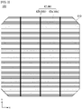
- FIG. 2 is a schematic plan view of a solar cell shown in FIG. 1 .
- a solar cell 100 includes a semiconductor substrate 110, a first conductivity-type region 20 formed on a first surface (e.g. a rear surface) of the semiconductor substrate 110 and composed of a polycrystalline silicon layer having a first conductivity type (e.g. n-type conductivity type), a first passivation layer 22 positioned on the first conductivity-type region 20, and a first electrode 42 electrically connected to the first conductivity-type region 20 passing through the first passivation layer 22.
- the solar cell 100 according to the present embodiment may include a second conductivity type region 30 formed at or on a second surface (e.g. a front surface) of the semiconductor substrate 110 and having a second conductivity type (e.g. p-type conductivity), a second passivation layer 32 positioned on the second conductivity-type region 30, and a second electrode 44 electrically connected to the second conductivity-type region 30 passing through the second passivation layer 32. This will be described in more detail.
- the semiconductor substrate 110 may be formed of a crystalline semiconductor.
- the semiconductor substrate 110 may be formed of a single crystal semiconductor or polycrystalline semiconductor (e.g. single crystal silicon or polycrystalline silicon).
- the semiconductor substrate 110 may be formed of a single crystal semiconductor (e.g. a single crystal semiconductor wafer, more specifically, a single crystal silicon wafer).
- the solar cell 100 constitutes a single crystal semiconductor solar cell (e.g. single crystal silicon solar cell).
- the solar cell 100 based on the semiconductor substrate 110 formed of a crystalline semiconductor having high crystallinity and fewer defects may have excellent electrical characteristics.
- the semiconductor substrate 110 may include the base region 10 having the first or second conductivity type by including a first or second conductivity-type dopant at a relatively low doping concentration.
- the first and second conductivity-type regions 20 and 30 have a higher doping concentration than the base region 10 having a conductivity type different from that of the base region 10, or having the same conductivity type as the base region 10.
- the base region 10 may have a first conductivity type (e.g. an n-type conductivity type).
- the front surface and/or the rear surface of the semiconductor substrate 110 may be textured to have unevenness.
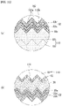
- the front surface and/or the rear surface of the semiconductor substrate 110 may have unevenness 112 and 114 formed by texturing.
- the unevenness 112 and 114 are formed on the front and/or rear surfaces of the semiconductor substrate 110 by such texturing, reflectivity of light incident through the front and/or rear surfaces of the semiconductor substrate 110 may be reduced. Accordingly, the amount of light reaching the pn junction formed by the base region 10 and the second conductivity-type region 30 can be increased, thereby minimizing light loss.
- the unevenness 112 and 114 may include a first unevenness 112 formed on the front surface (front side surface) of the semiconductor substrate 110 and a second unevenness 114 formed on the rear surface (rear side surface) of the semiconductor substrate 110. Accordingly, both reflection of light incident to the front and rear surfaces of the semiconductor substrate 110 may be prevented, so that light loss in the solar cell 100 having a bifacial structure as in the present embodiment can be effectively reduced.
- the present disclosure is not limited thereto.
- the first unevenness 112 may be provided on the front surface of the semiconductor substrate 110, but the second unevenness 114 may not be provided on the rear surface of the semiconductor substrate 110.
- first unevenness 112 may not be provided on the front surface of the semiconductor substrate 110, but the second unevenness 114 may be provided on the rear surface of the semiconductor substrate 110.
- first unevenness 112 and the second unevenness 114 may not be provided on the semiconductor substrate 110.
- the second unevenness 114 of the semiconductor substrate 110 has only the first uneven portion 114a and has a different shape from the first unevenness 112 having the first and second uneven portions 112a and 112b, reflection from the front surface of the semiconductor substrate 110 having a large incident amount of light can be effectively prevented by the first unevenness 112, and the second unevenness 114 may have a simple structure, thereby simplifying the manufacturing process of the solar cell 100.
- a thickness of the tunneling layer 52 may be smaller than a thickness of the first or second passivation layers 22 and 32 to sufficiently implement the tunneling effect.
- the thickness of the tunneling layer 52 may be 10 nm or less, and may be 0.5 nm to 10 nm (more specifically, 0.5 nm to 5 nm, for example, 1 nm to 4 nm).
- the thickness of the tunneling layer 52 exceeds 10 nm, tunneling does not occur smoothly and the solar cell 100 may not operate, and when the thickness of the tunneling layer 52 is less than 0.5 nm, it may be difficult to form the tunneling layer 52 of a desired quality.
- the first conductivity-type region 20 forms a rear electric field to prevent loss of carriers by recombination on the surface of the semiconductor substrate 110 (more precisely, the rear surface of the semiconductor substrate 110).
- the first passivation layer 22 may be positioned on the first conductivity-type region 20, and may include a first aluminum oxide layer 22a having hydrogen, and a first dielectric layer 22b positioned on the first aluminum oxide layer 22a and including a different material from that of the first aluminum oxide layer 22a.
- the second passivation layer 32 may include a second aluminum oxide layer 32a positioned on the second conductivity-type region 30, and a second dielectric layer 32b positioned on the second aluminum oxide layer 32a and including a different material from that of the second aluminum oxide layer 32a.
- the first aluminum oxide layer 22a positioned adjacent to the first conductivity-type region 20 composed of the polycrystalline semiconductor layer may serve as a hydrogen implantation layer for implementing hydrogen passivation by implanting hydrogen into the semiconductor substrate 110 and/or the first conductivity type region 20.
- the second aluminum oxide layer 32a positioned adjacent to the semiconductor substrate 110 may serve as a fixed charge passivation layer that prevents recombination using fixed charges. This will be described in more detail after the first dielectric layer 22b and the second dielectric layer 32b are described.
- the first dielectric layer 22b positioned on the first aluminum oxide layer 22a may serve as a capping layer that prevents hydrogen from being emitted to the outside in the annealing process of implanting hydrogen into the first aluminum oxide layer 22a functioning as a hydrogen implantation layer.
- the first electrode 42 when it has a predetermined pattern and has a double-sided light-receiving structure in which light is incident on both sides, it may serve as an anti-reflection layer to prevent reflection of light incident on the rear surface of the semiconductor substrate 110.
- it may serve as a protective layer covering the first aluminum oxide layer 22a to protect the first aluminum oxide layer 22a from an external acidic substance or the like. Accordingly, reliability is more excellent when used as a stacked structure of the first aluminum oxide layer 22a and the first dielectric layer 22b compared to the case of using the first aluminum oxide layer 22a alone.
- the first aluminum oxide layer 22a positioned adjacent to the first conductivity-type region 20 composed of the polycrystalline semiconductor layer (especially n-type polycrystalline semiconductor layer) and the second aluminum oxide layer 32a positioned adjacent to the semiconductor substrate 110 (especially the p-type second conductivity-type region 30) may play different roles. More specifically, the first aluminum oxide layer 22a may serve as a hydrogen implantation layer, and the second aluminum oxide layer 32a may serve as a fixed charge passivation layer. This will be described in more detail with reference to FIGS. 5 and 6 .
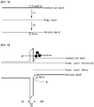
- FIG. 5 is a schematic diagram for explaining a recombination model due to a defect (trap site) and fixed charge passivation for preventing it.
- FIG. 6 is a diagram illustrating a band diagram of a semiconductor substrate, a tunneling layer, and a first conductivity-type region in a solar cell according to an embodiment of the present disclosure.
- Fixed charge passivation is to prevent the occurrence of recombination of electrons and holes by unbinding electrons bound to the trap level by the process shown by the arrow (1) of FIG. 5 by the fixed charge included in the passivation layer. In this case, since the unoccupied trap level continues to exist, the process as shown by the arrows (1) and (2) of FIG. 5 is repeated again, and the recombination may occur.
- the first and second electrodes 42 and 44 may have metal electrode layers made of various conductive materials (e.g. metal) and may have various shapes.
- the second electrode 44 may include a finger electrode 44a and a bus bar electrode 44b corresponding to the finger electrode 42a and the bus bar electrode 42b of the first electrode 42, respectively.
- the finger electrode 44a and the bus bar electrode 44b of the second electrode 44 the contents of the finger electrode 42a and the bus bar electrode 42b of the first electrode 42 may be applied as they are.
- the width and pitch of the finger electrodes 42a of the first electrode 42 may be the same as or different from the width and pitch of the finger electrodes 44a of the second electrode 44.
- the width of the bus bar electrode 42b of the first electrode 42 may be the same as or different from the width of the bus bar electrode 44b of the second electrode 44, but the bus bar electrode 42b of the first electrode 42 and the bus bar electrode 44b of the second electrode 44 may be disposed to have the same pitch at the same position.
- the solar cell 100 has a double-sided light-receiving structure in which light can be incident to the front and rear surfaces of the semiconductor substrate 110. Accordingly, it is possible to contribute to the improvement of the efficiency of the solar cell 100 by increasing the amount of light used in the solar cell 100.
- the present disclosure is not limited thereto. Accordingly, it is possible that the first electrode 42 and the second electrode 44 have different planar shapes. Various other variations are possible.
- the solar cell 100 having the bus bar electrode 42b having such a shape may be connected to a neighboring solar cell 100 or an external circuit using a wire-shaped wiring material (interconnector).
- the wire-shaped wiring material may have a smaller width than a ribbon having a relatively wide width (e.g. greater than 1 mm).
- the maximum width of the wiring member may be 1 mm or less (e.g. 500 ⁇ m or less, more specifically, 250 to 500 ⁇ m).
- the second conductivity-type region 30 composed of a doped region and the first conductivity-type region 20 composed of a semiconductor layer, it is possible to minimize incident interference of light from the front surface of the semiconductor substrate 110 and to minimize the degradation of recombination characteristics due to the first conductivity-type region 20. Accordingly, the characteristics of the solar cell 100 may be improved.
- the method of manufacturing the solar cell 100 includes a tunneling layer forming step S12, a semiconductor layer forming step S14, a first etching step S16, a second etching step S18, a doping step S20, an aluminum oxide layer forming step S22, a dielectric layer forming step (a first annealing step) S24, a second annealing step S26, and an electrode forming step S28.
- the semiconductor substrate 110 having the first uneven portions 112a and 114a is prepared.
- the first uneven portion 112a of the first unevenness 112 may be provided on the front surface of the semiconductor substrate 110
- the first uneven portion 114a of the second unevenness 114 may be provided on the rear surface of the semiconductor substrate 110.
- the first uneven portions 112a and 114a are etched according to the crystal plane of the semiconductor substrate 110, the outer surfaces of the first uneven portions 112a and 114a are formed to have a constant crystal plane (e.g. (111) plane). Accordingly, the first uneven portions 112a and 114a may have a pyramid shape having four (111) planes, may have an average size of a micrometer level, and may have a relatively large first deviation in size deviation.
- the present disclosure is not limited thereto, and the first uneven portions 112a and 114a may be formed by various methods and may have various shapes, average sizes, size deviations, and the like.
- the present disclosure is not limited thereto, and it is also possible that the first uneven portions 112a and 114a are formed on one of the front surface, the rear surface, and the side surface of the semiconductor substrate 110. Alternatively, it is also possible that the first uneven portions 112a and 114a are not formed on the front surface, the rear surface, and the side surface of the semiconductor substrate 110.
- the tunneling layer 52 may be formed by, for example, a thermal growth method, a vapor deposition method (e.g. plasma-enhanced chemical vapor deposition (PECVD), atomic layer deposition (ALD)), or the like.
- a thermal growth method e.g. plasma-enhanced chemical vapor deposition (PECVD), atomic layer deposition (ALD)
- PECVD plasma-enhanced chemical vapor deposition
- ALD atomic layer deposition
- the present disclosure is not limited thereto, and the tunneling layer 52 may be formed by various methods.
- the semiconductor layer 202 When the semiconductor layer 202 is formed of the polycrystalline semiconductor layer including the first conductivity-type dopant, the semiconductor layer 202 may be viewed as the first conductivity-type region (reference numeral 20 in FIG. 10F , hereinafter the same). Therefore, in this case, it can be considered that the first conductivity-type region 20 is formed by the process of forming the semiconductor layer 202 .
- the first etching step S16 will be described in more detail when the second etching step S18 performed in the process shown in FIG. 10E is described.
- the second etching step S18 of forming the second uneven portion 112b on the front surface of the semiconductor substrate 110 is performed.
- the first etching step S16 and the second etching step S18 are performed by reactive ion etching (RIE), but the process conditions may be different from each other.
- the reactive ion etching is a dry etching method of etching by generating plasma after supplying an etching gas (e.g. Cl 2 , SF 6 , NF 3 , HBr, etc.).
- the reactive ion etching may be applied to cross-sectional etching.
- the material may be etched basically isotropically without considering the crystal direction, etc. of the crystal grains.
- the semiconductor layer 202 and/or the tunneling layer 52 positioned on the front surface of the semiconductor substrate 110 may be entirely removed, and the second uneven portion 112b may be formed by etching one surface of the semiconductor substrate 110.
- the second uneven portion 112b of the first unevenness 112 formed by the second etching step S18 is formed on the outer surface of the first uneven portion 112a, and has an average size smaller than that of the uneven portion 112a of the first unevenness 112.
- the reactive ion etching may form the fine and uniform second uneven portion 112b on the surface of the semiconductor substrate 110 regardless of the crystal direction of the crystal grains.
- the second uneven portion 112b may be formed to have a sharp upper end, may have an average size of a nanometer level, and may have a second deviation in which the size deviation is smaller than the first deviation.
- the second uneven portion 112b having an average size smaller than this is formed, thus it is possible to minimize the reflectivity that may occur on the surface of the semiconductor substrate 110.
- the first unevenness 112 includes the first uneven portion 112a and the second uneven portion 112b
- the second unevenness 114 includes the first uneven portion 114a and does not include the second uneven portion 112b. Since the second etching step S18 of forming the second uneven portion 112b is performed after the first etching step S16 of etching the semiconductor layer 202, the rear surface of the semiconductor substrate 110 is covered by the semiconductor layer 202, and the second etching step S18 is performed by the cross-sectional etching. Accordingly, the second uneven portion 112b is formed on the front surface of the semiconductor substrate 110 and the second uneven portion 112b is not formed on the rear surface of the semiconductor substrate 110. Accordingly, the passivation characteristics may be improved by minimizing the surface area of the rear surface of the semiconductor substrate 110, which is relatively small in incidence of light, and minimizing damage caused by the reactive ion etching.
- first etching step S16 and the second etching step S18 may be performed by separate devices or processes, and the second etching step S18 may not be performed.
- first etching step S16 and the second etching step S18 may be performed by separate devices or processes, and the second etching step S18 may not be performed.
- Various other variations are possible.
- the second conductivity-type region 30 is formed by doping or diffusing the second conductivity-type dopant.
- the first conductivity-type dopant of the semiconductor layer 202 or the first conductivity-type region 20 may be doped, diffused, or activated together.
- the method of forming the first conductivity-type region 20 and the second conductivity-type region 30 may use various known methods.
- the first conductivity-type region 20 may be formed based on the semiconductor layer 202.
- the first conductivity type region 20 is formed by doping or diffusing the first conductivity-type dopant.
- Various methods may be used as a method of doping or diffusing the first conductivity-type dopant into the semiconductor layer 202.
- the first conductivity-type region 20 may be formed by doping or diffusing the first conductivity-type dopant by a method such as an ion implantation method, a thermal diffusion method, or a laser doping method.
- a heat treatment process for activation of the first conductivity-type dopant may be additionally performed. The heat treatment process for activation is not essential and may be omitted depending on a doping method or the like.
- the first conductivity-type region 20 is formed by diffusing the first conductivity-type dopant by performing the heat treatment process while forming a first dopant film (e.g. phosphorus silicate glass (PSG) film) including the first conductivity-type dopant on the semiconductor layer 202
- a first dopant film e.g. phosphorus silicate glass (PSG) film
- the first dopant film may be formed by various methods, such as atmospheric pressure chemical vapor deposition (APCVD), plasma enhanced chemical vapor deposition (PECVD), or the like.
- APCVD atmospheric pressure chemical vapor deposition
- PECVD plasma enhanced chemical vapor deposition
- an ion implantation method or a method of forming the first dopant film may be advantageous for a cross-sectional doping.
- the intrinsic semiconductor layer 202 may be more easily etched in the first etching step S16, etc.
- the first conductivity-type region 20 may be formed or activated by doping, diffusing, or activating the first conductivity-type dopant included in the semiconductor layer 202 through the heat treatment process.
- the semiconductor layer 202 may include a doped layer including the first conductivity-type dopant and an undoped layer not including the first conductivity-type dopant, and may form the first conductivity-type region 20 by doping and diffusing the first conductivity-type dopant of the doped layer into the undoped layer in the heat treatment process.
- the semiconductor layer 202 when the semiconductor layer 202 is formed, the semiconductor layer 202 may be formed to have the first conductivity-type using a gas (e.g. PH 3 gas) including the first conductivity-type dopant. Then, since the semiconductor layer 202 forms the first conductivity-type region 20 as it is without a separate doping process, a manufacturing process may be simplified by omitting a process for doping the semiconductor layer 202. Even in this case, a heat treatment process for activating the first conductivity-type dopant may be additionally performed. The heat treatment process for activation may be not essential and may be omitted depending on a doping method or the like. In addition, various modifications are possible.
- a gas e.g. PH 3 gas
- the second conductivity-type region 30 may be formed by doping or diffusing the second conductivity-type dopant into inside of the semiconductor substrate 110 from the front surface of the semiconductor substrate 110.
- Various methods may be used as a method of doping or diffusing the second conductivity-type dopant on the front surface side of the semiconductor substrate 110.
- the second conductivity-type region 30 may be formed by doping or diffusing the second conductivity-type dopant by a partial thickness on the front surface of the semiconductor substrate 110 by a method such as an ion implantation method, a thermal diffusion method, or a laser doping method.
- a heat treatment process for activating the second conductivity-type dopant may be additionally performed.
- the heat treatment process for activation may be not essential and may be omitted depending on a doping method or the like.
- the second conductivity type region 30 is formed by diffusing the second conductivity-type dopant by performing the heat treatment process while forming a second dopant film (e.g. boron silicate glass (BSG) film) including the second conductivity-type dopant on the semiconductor substrate 110
- the second dopant film may be removed.
- the second dopant film may be formed by various methods, such as atmospheric pressure chemical vapor deposition (APCVD), plasma enhanced chemical vapor deposition (PECVD), or the like.
- APCVD atmospheric pressure chemical vapor deposition
- PECVD plasma enhanced chemical vapor deposition
- an ion implantation method or a method of forming the second dopant film may be advantageous for a cross-sectional doping.
- the heat treatment process for doping, diffusion, or activation to form the first conductivity-type region 20 and the heat treatment process for doping, diffusion, or activation to form the second conductivity-type region 30 may be performed simultaneously or separately from each other.
- the first conductivity-type dopant of the first conductivity-type region 20 and the second conductivity-type dopant of the second conductivity-type region 30 may be activated together by co-activation heat treatment.
- the co-activation heat treatment may be performed at various temperatures capable of activating the first conductivity-type dopant and the second conductivity-type dopant together.
- the present disclosure is not limited thereto.
- an activation heat treatment is performed after forming the second conductivity-type region 30, and then an activation heat treatment is performed after forming the first conductivity-type region 20, and it is also possible to separately perform the activation heat treatment of the first and second conductivity-type regions 20 and 30.
- Various other variations are possible.
- the second conductivity-type dopant may be doped first and the first conductivity-type dopant may be doped later, or the first conductivity-type dopant may be doped first and the second conductivity-type dopant may be doped later.
- the first and second conductivity-type regions 20 and 30 may be formed together by heat treatment in a state in which the first dopant film for forming the first conductivity-type region 20 and the second dopant film for forming the second conductivity-type region 30 are formed together, and then the first and second dopant films may be removed.
- the first and second dopant films may be removed.
- a cleaning process may be performed to remove by-products, etc. remaining during the doping, diffusion, or activation heat treatment process.
- a passivation layer forming step including forming the first passivation layer 22 on the rear surface of the semiconductor substrate 110 and forming the second passivation layer 32 on the front surface of the semiconductor substrate 110 is performed.
- the forming of the first passivation layer 22 may include a process of forming the first aluminum oxide layer 22a having hydrogen on the first conductivity-type region 20, and a process of forming the first dielectric layer 22b positioned on the first aluminum oxide layer 22a and including a material different from the first aluminum oxide layer 22a.
- the forming of the second passivation layer 32 may include a process of forming the second aluminum oxide layer 32a on the second conductivity-type region 30, and a process of forming the second dielectric layer 32b positioned on the second aluminum oxide layer 32a and including a material different from the aluminum oxide layer 32a.
- hydrogen included in the first aluminum oxide layer 22a may be implanted into the first conductivity-type region 20 and/or the semiconductor substrate 110 by an annealing process performed in the passivation layer forming step and/or the electrode formation step, which will be described in more detail.
- the process of forming the first aluminum oxide layer 22a and the process of forming the second aluminum oxide layer 32a may be performed to form the first and second aluminum oxide layers 22a and 32a in the aluminum oxide layer forming step S22.
- the process of forming the first aluminum oxide layer 22a and the process of forming the second aluminum oxide layer 32a may be performed together by the same process, so that the first aluminum oxide layer 22a and the second aluminum oxide layer 32a may be formed together in the same process.
- the first aluminum oxide layer 22a and the second aluminum oxide layer 32a may be composed of the same layer having the same material, composition, and thickness. As described above, when the first aluminum oxide layer 22a and the second aluminum oxide layer 32a are formed together in the same process, the process may be simplified.
- the drawing illustrates that the first aluminum oxide layer 22a and the second aluminum oxide layer 32a are formed separately from each other
- the first aluminum oxide layer 22a and/or the second aluminum oxide layer 32a may be formed entirely on the surface of the semiconductor substrate 110 by forming not only the front and rear surfaces but also the side surface of the semiconductor substrate 110.
- the first aluminum oxide layer 22a formed on the rear surface of the semiconductor substrate 110 and the second aluminum oxide layer 32a formed on the front surface of the semiconductor substrate 110 may be connected to each other from the side surface, so that the aluminum oxide layer formed on the front surface, the side surface, and the rear surface may have a shape continuously connected to each other.
- the process of forming the first aluminum oxide layer 22a and the process of forming the second aluminum oxide layer 32a may be separately performed to form the first and second aluminum oxide layers 22a and 32a in separate processes.
- the first aluminum oxide layer 22a and the second aluminum oxide layer 32a may be the same layer having the same material, composition, and thickness, or may be different layers having different materials, compositions, or thicknesses.
- the first aluminum oxide layer 22a and/or the second aluminum oxide layer 32a may be formed by various methods, for example, it may be formed by an atomic layer deposition method (ALD), a plasma-induced chemical vapor deposition method, or the like.
- ALD atomic layer deposition method
- the first aluminum oxide layer 22a and/or the second aluminum oxide layer 32a may be formed by an atomic layer deposition method using H 2 O, trimethylamine (TMA), or the like as a raw material.
- TMA trimethylamine
- a second dielectric layer 32b is formed in the second dielectric layer forming step S24.
- the second dielectric layer 32b may be made of silicon nitride, silicon oxide, or silicon oxynitride, and may be, for example, a silicon nitride layer made of silicon nitride.
- the second dielectric layer forming step S24 may include a first annealing process and a deposition process performed after the first annealing process. That is, the first annealing process may be performed before the deposition process in the second dielectric layer forming step S24.
- the first annealing process and the deposition process may be performed by an in-situ process that is continuously performed in the same equipment.
- the first annealing process may be a process in which hydrogen included in the first aluminum oxide layer 22a is implanted into the first conductivity type region 20 and/or the semiconductor substrate 110, and may be performed at a temperature, in a gas atmosphere, etc. suitable for hydrogen implantation.
- the first annealing process may be performed at a temperature of 300 to 600° C, in a nitrogen (N 2 ) atmosphere.
- the deposition process may be performed at a temperature, a gas atmosphere, or the like at which the second dielectric layer 32b may be formed.
- the deposition process may be performed by atmospheric pressure chemical vapor deposition or plasma-induced chemical vapor deposition performed in a gas atmosphere of silane (SiH 4 ) or ammonia (NH 3 ).
- a first dielectric layer 22b is formed in the first dielectric layer forming step S26.
- the first dielectric layer 22b may be made of silicon nitride, silicon oxide, or silicon oxynitride, and may be, for example, a silicon nitride layer made of silicon nitride.
- the first dielectric layer forming step S26 may include a deposition process.
- the deposition process may be performed at a temperature, a gas atmosphere, or the like at which the first dielectric layer 22b can be formed.
- the deposition process may be performed by atmospheric pressure chemical vapor deposition or plasma-induced chemical vapor deposition performed in a gas atmosphere of silane (SiH 4 ) or ammonia (NH 3 ).
- the first and second electrodes 42 and 44 respectively connected to the first conductivity-type region 20 and the second conductivity-type region 30 are formed in the electrode formation step S28.
- the first and second electrodes 42 and 44 may be formed while forming the openings 102 and 104 by fire-through or laser firing contact, etc. In this case, since the openings 102 and 104 are formed when the first and second electrodes 42 and 44 are fired, there is no need to add a separate process for forming the openings 102 and 104.
- a second annealing process of implanting hydrogen included in the first aluminum oxide layer 22a into the first conductivity-type region 20 and/or the semiconductor substrate 110 may be performed by a process of firing the first and second electrodes 42 and 44. That is, when a firing process performed at a relatively high temperature (e.g. a higher temperature than the first annealing process) is performed in the step of forming the first and second electrodes 42 and 44, hydrogen included in the first aluminum oxide layer 22a may be effectively implanted into the first conductivity-type region 20 and/or the semiconductor substrate 110 due to the high temperature of the firing process.
- the first dielectric layer 22b serves as a capping layer that prevents out-diffusion of hydrogen included in the first aluminum oxide layer 22a. Hydrogen may be effectively implanted into the first conductivity-type region 20 and/or the semiconductor substrate 110 due to the high temperature of the firing process and the first aluminum oxide layer 22a serving as a capping layer.
- the openings 102 and 104 may be respectively formed in the first passivation layer 22 and the second passivation layer 32, and the first and second electrodes 42 and 44 may be formed in the openings 102 and 104 using various methods such as plating method and vapor deposition method.
- the semiconductor layer 202 and/or the tunneling layer 52 positioned on the front surface of the semiconductor substrate 110 are removed by the first etching step S16.
- the second conductivity-type region 30 is configured as a doped region formed by doping (or diffusing) the second conductivity-type dopant into the semiconductor substrate 110.
- the first conductivity-type region 20 is formed based on the semiconductor layer 202 formed on the tunneling layer 52 and is formed of a semiconductor layer having a crystal structure different from that of the semiconductor substrate 110.
- the characteristics of the solar cell 100 may be greatly improved.
- hydrogen passivation may occur by implanting hydrogen included in the first aluminum oxide layer 22a into the first conductivity-type region 20 and/or the semiconductor substrate 110 through the first annealing process and/or the second annealing process, thereby improving passivation characteristics in the solar cell 100 having the first conductivity-type region 20 formed of a semiconductor layer (especially, n-type semiconductor layer). Accordingly, the efficiency of the solar cell 100 can be improved through a simple process.
- the silicon oxide layers 20a and 30a may be formed and positioned between the first conductivity-type region 20 and the first aluminum oxide layer 22a and/or between the second conductivity-type region 30 and the second aluminum oxide layer 32b.
- the silicon oxide layers 20a and 30a may be provided together with the first and/or second passivation layers 20 and 30 to further improve the passivation characteristics.
- the present disclosure is not limited thereto.
- a plurality of solar cells having a structure as shown in FIG. 1 are manufactured. More specifically, by preparing a single crystal silicon substrate having phosphorus as a base dopant, a first conductivity type region composed of a tunneling layer composed of a silicon oxide layer and a polycrystalline silicon layer including phosphorus (P) as a first conductivity-type dopant is formed, and a second conductivity-type region composed of a doped region including boron as a second conductivity-type dopant is formed. First and second aluminum oxide layers are simultaneously formed on the first and second conductivity-type regions by using an atomic layer deposition method. A second dielectric layer composed of a silicon nitride layer is formed on the second aluminum oxide layer.
- a deposition process of forming a silicon nitride layer after performing the first annealing process may be performed at a temperature of 550° C and a nitrogen atmosphere in the process of forming the second dielectric layer. Then, a deposition process is performed on the first aluminum oxide layer to form a first dielectric layer composed of a silicon nitride layer. Then, after the paste for forming the first electrode and the paste for forming the second electrode are applied on the first passivation layer and the second passivation layer by screen printing, they are fired, while performing the second annealing process, the first and second electrodes connected to the first and second conductivity-type regions are formed by fire-through.
- a plurality of solar cells are manufactured in the same manner as in Embodiment 1, except that the process of forming the first and second aluminum oxide layers and the first annealing process are not performed, so that the first and second passivation layers each are made of only a silicon nitride layer.
- a plurality of solar cells are manufactured in the same manner as in Embodiment 1, except that the process of forming the first and second dielectric layers is not performed, so that the first and second passivation layers each are made of only an aluminum oxide layer.
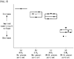
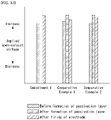
- the implied open-circuit voltages of the solar cells according to Embodiment 1 and Comparative Examples 1 and 2 are measured, and the results are shown in FIG. 12 .
- the implied open-circuit voltages are measured before the passivation layer formation, after the passivation layer formation, and after the electrode firing in the plurality of solar cells, and the average values thereof are shown together in FIG. 12 .
- the implicit open-circuit voltage of the solar cell according to Embodiment 1 is greatly increased after the formation of the passivation layer and after the electrode firing compared to the solar cells according to Comparative Examples 1 and 2. This is expected because the passivation characteristics are improved by the first passivation layer including the first aluminum oxide layer and the first dielectric layer, and the second passivation layer including the second aluminum oxide layer and the second dielectric layer.
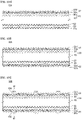
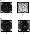
- FIGS. 13 and 14 A photoluminescence (PL) photograph is taken by selecting a solar cell using a semiconductor substrate manufactured in the same or similar portion of an ingot from among the plurality of solar cells manufactured according to Embodiment 1 and Comparative Example 1, and the results are shown in FIGS. 13 and 14 .
- FIG. 13(a) shows a photoluminescence photograph after forming the first and second conductivity-type regions in Embodiment 1
- FIG. 13(b) shows a photoluminescence photograph after forming the first and second passivation layers in Embodiment 1.
- FIG. 14(a) shows a photoluminescence photograph after forming the first and second conductivity-type regions in Comparative Example 1
- FIG.14(b) shows a photoluminescence photograph after forming the first and second passivation layers in Comparative Example 1.
Landscapes
- Photovoltaic Devices (AREA)
- Chemical & Material Sciences (AREA)
- Crystallography & Structural Chemistry (AREA)
- Life Sciences & Earth Sciences (AREA)
- Engineering & Computer Science (AREA)
- Sustainable Development (AREA)
- Sustainable Energy (AREA)
Applications Claiming Priority (2)
| Application Number | Priority Date | Filing Date | Title |
|---|---|---|---|
| KR1020190087537A KR20210010095A (ko) | 2019-07-19 | 2019-07-19 | 태양 전지 및 이의 제조 방법 |
| PCT/KR2020/004845 WO2021015395A2 (ko) | 2019-07-19 | 2020-04-09 | 태양 전지 및 이의 제조 방법 |
Publications (2)
| Publication Number | Publication Date |
|---|---|
| EP4002495A2 true EP4002495A2 (de) | 2022-05-25 |
| EP4002495A4 EP4002495A4 (de) | 2023-07-19 |
Family
ID=74193517
Family Applications (1)
| Application Number | Title | Priority Date | Filing Date |
|---|---|---|---|
| EP20844936.3A Pending EP4002495A4 (de) | 2019-07-19 | 2020-04-09 | Solarzelle und herstellungsverfahren dafür |
Country Status (5)
| Country | Link |
|---|---|
| US (3) | US12543400B2 (de) |
| EP (1) | EP4002495A4 (de) |
| KR (2) | KR20210010095A (de) |
| CN (4) | CN119069575A (de) |
| WO (1) | WO2021015395A2 (de) |
Cited By (2)
| Publication number | Priority date | Publication date | Assignee | Title |
|---|---|---|---|---|
| AU2022209315A1 (en) * | 2022-05-31 | 2023-12-14 | Zhejiang Jinko Solar Co., Ltd. | Solar Cell and Manufacture Method thereof, and Photovoltaic Module |
| US12113139B1 (en) | 2023-09-28 | 2024-10-08 | Zhejiang Jinko Solar Co., Ltd. | Solar cell and photovoltaic module |
Families Citing this family (11)
| Publication number | Priority date | Publication date | Assignee | Title |
|---|---|---|---|---|
| CN113611774A (zh) * | 2021-07-26 | 2021-11-05 | 泰州中来光电科技有限公司 | 一种钝化接触电池的电极金属化方法及电池、组件和系统 |
| KR20230100022A (ko) * | 2021-12-28 | 2023-07-05 | 엘지전자 주식회사 | 태양 전지 및 이의 제조 방법 |
| CN115692548B (zh) * | 2022-11-24 | 2024-10-11 | 通威太阳能(成都)有限公司 | 太阳电池及其制备方法 |
| CN115881835B (zh) | 2023-02-08 | 2024-05-14 | 浙江晶科能源有限公司 | 太阳能电池及其制备方法、光伏组件 |
| CN117650196A (zh) * | 2023-11-01 | 2024-03-05 | 天合光能股份有限公司 | 钝化接触结构及其制备方法、太阳能电池及其制备方法 |
| CN118053928A (zh) * | 2023-12-15 | 2024-05-17 | 浙江晶科能源有限公司 | 太阳能电池及光伏组件 |
| CN118053927A (zh) | 2023-12-15 | 2024-05-17 | 浙江晶科能源有限公司 | 太阳能电池及其制备方法、光伏组件 |
| CN119008726A (zh) | 2023-12-15 | 2024-11-22 | 浙江晶科能源有限公司 | 太阳能电池及其制备方法、光伏组件 |
| CN118053922A (zh) | 2023-12-15 | 2024-05-17 | 浙江晶科能源有限公司 | 太阳能电池及其制备方法、光伏组件 |
| KR102813486B1 (ko) * | 2024-07-29 | 2025-05-28 | (주)피앤테크 | 태양전지 및 그의 제조방법 |
| CN120129342B (zh) * | 2025-05-09 | 2025-08-19 | 晶科能源(海宁)有限公司 | 太阳能电池片的制作方法、太阳能电池片及光伏组件 |
Family Cites Families (13)
| Publication number | Priority date | Publication date | Assignee | Title |
|---|---|---|---|---|
| JP2004193350A (ja) * | 2002-12-11 | 2004-07-08 | Sharp Corp | 太陽電池セルおよびその製造方法 |
| US20080173347A1 (en) * | 2007-01-23 | 2008-07-24 | General Electric Company | Method And Apparatus For A Semiconductor Structure |
| TW200929575A (en) * | 2007-12-28 | 2009-07-01 | Ind Tech Res Inst | A passivation layer structure of the solar cell and the method of the fabricating |
| JP5649580B2 (ja) | 2009-09-18 | 2015-01-07 | 信越化学工業株式会社 | 太陽電池の製造方法 |
| US8110431B2 (en) | 2010-06-03 | 2012-02-07 | Suniva, Inc. | Ion implanted selective emitter solar cells with in situ surface passivation |
| FI20116217L (fi) * | 2011-12-02 | 2013-06-03 | Beneq Oy | Piitä sisältävä n-tyypin aurinkokennopari |
| WO2013100085A1 (ja) * | 2011-12-27 | 2013-07-04 | 京セラ株式会社 | 太陽電池素子、太陽電池素子の製造方法および太陽電池モジュール |
| KR101976420B1 (ko) | 2013-03-06 | 2019-05-09 | 엘지전자 주식회사 | 태양 전지 및 이의 제조 방법 |
| DE102013219561A1 (de) | 2013-09-27 | 2015-04-02 | Fraunhofer-Gesellschaft zur Förderung der angewandten Forschung e.V. | Verfahren zum Herstellen einer photovoltaischen Solarzelle mit zumindest einem Heteroübergang |
| KR101625876B1 (ko) * | 2014-07-18 | 2016-05-31 | 엘지전자 주식회사 | 태양 전지 및 이의 제조 방법 |
| KR102295984B1 (ko) * | 2014-11-04 | 2021-09-01 | 엘지전자 주식회사 | 태양 전지 |
| US9722104B2 (en) * | 2014-11-28 | 2017-08-01 | Lg Electronics Inc. | Solar cell and method for manufacturing the same |
| CN108987490B (zh) | 2018-07-18 | 2020-04-14 | 国家电投集团西安太阳能电力有限公司 | 太阳能电池湿法刻蚀氧化后表层清洁的处理方法 |
-
2019
- 2019-07-19 KR KR1020190087537A patent/KR20210010095A/ko not_active Ceased
-
2020
- 2020-04-09 US US17/627,541 patent/US12543400B2/en active Active
- 2020-04-09 CN CN202411202139.4A patent/CN119069575A/zh active Pending
- 2020-04-09 WO PCT/KR2020/004845 patent/WO2021015395A2/ko not_active Ceased
- 2020-04-09 CN CN202080052377.5A patent/CN114127961A/zh active Pending
- 2020-04-09 EP EP20844936.3A patent/EP4002495A4/de active Pending
- 2020-04-09 CN CN202411202133.7A patent/CN119069573A/zh active Pending
- 2020-04-09 CN CN202411202137.5A patent/CN119069574A/zh active Pending
-
2021
- 2021-10-20 KR KR1020210140207A patent/KR102549298B1/ko active Active
-
2024
- 2024-09-25 US US18/895,798 patent/US20250098362A1/en active Pending
- 2024-10-17 US US18/918,682 patent/US20250120216A1/en active Pending
Cited By (5)
| Publication number | Priority date | Publication date | Assignee | Title |
|---|---|---|---|---|
| AU2022209315A1 (en) * | 2022-05-31 | 2023-12-14 | Zhejiang Jinko Solar Co., Ltd. | Solar Cell and Manufacture Method thereof, and Photovoltaic Module |
| AU2022209315B2 (en) * | 2022-05-31 | 2024-01-11 | Zhejiang Jinko Solar Co., Ltd. | Solar Cell and Manufacture Method thereof, and Photovoltaic Module |
| US12166140B2 (en) | 2022-05-31 | 2024-12-10 | Zhejiang Jinko Solar Co., Ltd. | Solar cell and manufacture method thereof, and photovoltaic module |
| US12113139B1 (en) | 2023-09-28 | 2024-10-08 | Zhejiang Jinko Solar Co., Ltd. | Solar cell and photovoltaic module |
| EP4531113A1 (de) * | 2023-09-28 | 2025-04-02 | Zhejiang Jinko Solar Co., Ltd. | Solarzelle und fotovoltaisches modul |
Also Published As
| Publication number | Publication date |
|---|---|
| WO2021015395A3 (ko) | 2021-04-01 |
| US12543400B2 (en) | 2026-02-03 |
| KR20210131276A (ko) | 2021-11-02 |
| CN119069575A (zh) | 2024-12-03 |
| US20250120216A1 (en) | 2025-04-10 |
| KR102549298B1 (ko) | 2023-06-30 |
| CN119069573A (zh) | 2024-12-03 |
| CN114127961A (zh) | 2022-03-01 |
| WO2021015395A2 (ko) | 2021-01-28 |
| KR20210010095A (ko) | 2021-01-27 |
| US20250098362A1 (en) | 2025-03-20 |
| US20220262967A1 (en) | 2022-08-18 |
| EP4002495A4 (de) | 2023-07-19 |
| CN119069574A (zh) | 2024-12-03 |
Similar Documents
| Publication | Publication Date | Title |
|---|---|---|
| US20250098362A1 (en) | Solar cell and manufacturing method therefor | |
| EP3193376B1 (de) | Solarzelle und verfahren zur herstellung davon | |
| EP2804219B1 (de) | Solarzelle und verfahren zu ihrer herstellung | |
| EP2879189B1 (de) | Solarzelle und Verfahren zur Herstellung davon | |
| EP3098860B1 (de) | Verfahren zur herstellung einer solarzelle | |
| EP2797124B1 (de) | Verfahren zur Herstellung einer Solarzelle | |
| KR102272433B1 (ko) | 태양 전지 및 이의 제조 방법 | |
| KR102244838B1 (ko) | 태양 전지 및 이의 제조 방법 | |
| EP3200237B1 (de) | Solarzelle | |
| US20130344647A1 (en) | Method for manufacturing solar cell and dopant layer thereof | |
| US9608135B2 (en) | Solar cell and method for manufacturing the same | |
| US20130160840A1 (en) | Solar cell | |
| EP2662904B1 (de) | Verfahren zur herstellung von solarzellen | |
| US12593528B2 (en) | Solar cell and photovoltaic module | |
| KR102498523B1 (ko) | 태양 전지 및 이의 제조 방법 | |
| KR102336219B1 (ko) | 태양 전지 및 이의 제조 방법 | |
| KR102298671B1 (ko) | 태양 전지 및 이의 제조 방법 | |
| KR20150061169A (ko) | 태양 전지 및 이의 제조 방법 | |
| KR20170090781A (ko) | 태양 전지 및 이의 제조 방법 | |
| KR102219795B1 (ko) | 태양 전지 | |
| KR20150049213A (ko) | 태양 전지 | |
| KR20160005569A (ko) | 태양 전지의 제조 방법 |
Legal Events
| Date | Code | Title | Description |
|---|---|---|---|
| STAA | Information on the status of an ep patent application or granted ep patent |
Free format text: STATUS: THE INTERNATIONAL PUBLICATION HAS BEEN MADE |
|
| PUAI | Public reference made under article 153(3) epc to a published international application that has entered the european phase |
Free format text: ORIGINAL CODE: 0009012 |
|
| STAA | Information on the status of an ep patent application or granted ep patent |
Free format text: STATUS: REQUEST FOR EXAMINATION WAS MADE |
|
| 17P | Request for examination filed |
Effective date: 20220114 |
|
| AK | Designated contracting states |
Kind code of ref document: A2 Designated state(s): AL AT BE BG CH CY CZ DE DK EE ES FI FR GB GR HR HU IE IS IT LI LT LU LV MC MK MT NL NO PL PT RO RS SE SI SK SM TR |
|
| DAV | Request for validation of the european patent (deleted) | ||
| DAX | Request for extension of the european patent (deleted) | ||
| RAP1 | Party data changed (applicant data changed or rights of an application transferred) |
Owner name: SHANGRAO JINKO SOLAR TECHNOLOGY DEVELOPMENT CO., LTD |
|
| RAP1 | Party data changed (applicant data changed or rights of an application transferred) |
Owner name: SHANGRAO JINKO SOLAR TECHNOLOGY DEVELOPMENT CO., LTD |
|
| A4 | Supplementary search report drawn up and despatched |
Effective date: 20230616 |
|
| RIC1 | Information provided on ipc code assigned before grant |
Ipc: H01L 31/0236 20060101ALI20230612BHEP Ipc: H01L 31/0224 20060101ALI20230612BHEP Ipc: H01L 31/032 20060101ALI20230612BHEP Ipc: H01L 31/0368 20060101ALI20230612BHEP Ipc: H01L 31/18 20060101AFI20230612BHEP |
|
| RAP3 | Party data changed (applicant data changed or rights of an application transferred) |
Owner name: SHANGRAO XINYUAN YUEDONG TECHNOLOGY DEVELOPMENT CO. LTD |
|
| RAP1 | Party data changed (applicant data changed or rights of an application transferred) |
Owner name: TRINA SOLAR CO., LTD |