EP4002962B1 - Machine de moulage tridimensionnel et machine de montage de composant - Google Patents
Machine de moulage tridimensionnel et machine de montage de composant Download PDFInfo
- Publication number
- EP4002962B1 EP4002962B1 EP19937697.1A EP19937697A EP4002962B1 EP 4002962 B1 EP4002962 B1 EP 4002962B1 EP 19937697 A EP19937697 A EP 19937697A EP 4002962 B1 EP4002962 B1 EP 4002962B1
- Authority
- EP
- European Patent Office
- Prior art keywords
- component
- pallet
- molding
- mounting
- machine
- Prior art date
- Legal status (The legal status is an assumption and is not a legal conclusion. Google has not performed a legal analysis and makes no representation as to the accuracy of the status listed.)
- Active
Links
Images


Classifications
-
- H—ELECTRICITY
- H05—ELECTRIC TECHNIQUES NOT OTHERWISE PROVIDED FOR
- H05K—PRINTED CIRCUITS; CASINGS OR CONSTRUCTIONAL DETAILS OF ELECTRIC APPARATUS; MANUFACTURE OF ASSEMBLAGES OF ELECTRICAL COMPONENTS
- H05K13/00—Apparatus or processes specially adapted for manufacturing or adjusting assemblages of electric components
- H05K13/0061—Tools for holding the circuit boards during processing; handling transport of printed circuit boards
-
- B—PERFORMING OPERATIONS; TRANSPORTING
- B29—WORKING OF PLASTICS; WORKING OF SUBSTANCES IN A PLASTIC STATE IN GENERAL
- B29C—SHAPING OR JOINING OF PLASTICS; SHAPING OF MATERIAL IN A PLASTIC STATE, NOT OTHERWISE PROVIDED FOR; AFTER-TREATMENT OF THE SHAPED PRODUCTS, e.g. REPAIRING
- B29C64/00—Additive manufacturing, i.e. manufacturing of three-dimensional [3D] objects by additive deposition, additive agglomeration or additive layering, e.g. by 3D printing, stereolithography or selective laser sintering
- B29C64/10—Processes of additive manufacturing
- B29C64/106—Processes of additive manufacturing using only liquids or viscous materials, e.g. depositing a continuous bead of viscous material
- B29C64/112—Processes of additive manufacturing using only liquids or viscous materials, e.g. depositing a continuous bead of viscous material using individual droplets, e.g. from jetting heads
-
- B—PERFORMING OPERATIONS; TRANSPORTING
- B29—WORKING OF PLASTICS; WORKING OF SUBSTANCES IN A PLASTIC STATE IN GENERAL
- B29C—SHAPING OR JOINING OF PLASTICS; SHAPING OF MATERIAL IN A PLASTIC STATE, NOT OTHERWISE PROVIDED FOR; AFTER-TREATMENT OF THE SHAPED PRODUCTS, e.g. REPAIRING
- B29C64/00—Additive manufacturing, i.e. manufacturing of three-dimensional [3D] objects by additive deposition, additive agglomeration or additive layering, e.g. by 3D printing, stereolithography or selective laser sintering
- B29C64/20—Apparatus for additive manufacturing; Details thereof or accessories therefor
- B29C64/227—Driving means
- B29C64/236—Driving means for motion in a direction within the plane of a layer
-
- B—PERFORMING OPERATIONS; TRANSPORTING
- B29—WORKING OF PLASTICS; WORKING OF SUBSTANCES IN A PLASTIC STATE IN GENERAL
- B29C—SHAPING OR JOINING OF PLASTICS; SHAPING OF MATERIAL IN A PLASTIC STATE, NOT OTHERWISE PROVIDED FOR; AFTER-TREATMENT OF THE SHAPED PRODUCTS, e.g. REPAIRING
- B29C64/00—Additive manufacturing, i.e. manufacturing of three-dimensional [3D] objects by additive deposition, additive agglomeration or additive layering, e.g. by 3D printing, stereolithography or selective laser sintering
- B29C64/20—Apparatus for additive manufacturing; Details thereof or accessories therefor
- B29C64/245—Platforms or substrates
-
- B—PERFORMING OPERATIONS; TRANSPORTING
- B29—WORKING OF PLASTICS; WORKING OF SUBSTANCES IN A PLASTIC STATE IN GENERAL
- B29C—SHAPING OR JOINING OF PLASTICS; SHAPING OF MATERIAL IN A PLASTIC STATE, NOT OTHERWISE PROVIDED FOR; AFTER-TREATMENT OF THE SHAPED PRODUCTS, e.g. REPAIRING
- B29C64/00—Additive manufacturing, i.e. manufacturing of three-dimensional [3D] objects by additive deposition, additive agglomeration or additive layering, e.g. by 3D printing, stereolithography or selective laser sintering
- B29C64/30—Auxiliary operations or equipment
-
- H—ELECTRICITY
- H05—ELECTRIC TECHNIQUES NOT OTHERWISE PROVIDED FOR
- H05K—PRINTED CIRCUITS; CASINGS OR CONSTRUCTIONAL DETAILS OF ELECTRIC APPARATUS; MANUFACTURE OF ASSEMBLAGES OF ELECTRICAL COMPONENTS
- H05K1/00—Printed circuits
- H05K1/02—Details
- H05K1/0284—Details of three-dimensional rigid printed circuit boards
-
- H—ELECTRICITY
- H05—ELECTRIC TECHNIQUES NOT OTHERWISE PROVIDED FOR
- H05K—PRINTED CIRCUITS; CASINGS OR CONSTRUCTIONAL DETAILS OF ELECTRIC APPARATUS; MANUFACTURE OF ASSEMBLAGES OF ELECTRICAL COMPONENTS
- H05K1/00—Printed circuits
- H05K1/18—Printed circuits structurally associated with non-printed electric components
- H05K1/182—Printed circuits structurally associated with non-printed electric components associated with components mounted in printed circuit boards [PCB], e.g. insert-mounted components [IMC]
- H05K1/183—Printed circuits structurally associated with non-printed electric components associated with components mounted in printed circuit boards [PCB], e.g. insert-mounted components [IMC] associated with components mounted in and supported by recessed areas of the PCBs
-
- H—ELECTRICITY
- H05—ELECTRIC TECHNIQUES NOT OTHERWISE PROVIDED FOR
- H05K—PRINTED CIRCUITS; CASINGS OR CONSTRUCTIONAL DETAILS OF ELECTRIC APPARATUS; MANUFACTURE OF ASSEMBLAGES OF ELECTRICAL COMPONENTS
- H05K13/00—Apparatus or processes specially adapted for manufacturing or adjusting assemblages of electric components
- H05K13/04—Mounting of components, e.g. of leadless components
- H05K13/0417—Feeding with belts or tapes
-
- H—ELECTRICITY
- H05—ELECTRIC TECHNIQUES NOT OTHERWISE PROVIDED FOR
- H05K—PRINTED CIRCUITS; CASINGS OR CONSTRUCTIONAL DETAILS OF ELECTRIC APPARATUS; MANUFACTURE OF ASSEMBLAGES OF ELECTRICAL COMPONENTS
- H05K13/00—Apparatus or processes specially adapted for manufacturing or adjusting assemblages of electric components
- H05K13/04—Mounting of components, e.g. of leadless components
- H05K13/0452—Mounting machines or lines comprising a plurality of tools for guiding different components to the same mounting place
-
- H—ELECTRICITY
- H05—ELECTRIC TECHNIQUES NOT OTHERWISE PROVIDED FOR
- H05K—PRINTED CIRCUITS; CASINGS OR CONSTRUCTIONAL DETAILS OF ELECTRIC APPARATUS; MANUFACTURE OF ASSEMBLAGES OF ELECTRICAL COMPONENTS
- H05K13/00—Apparatus or processes specially adapted for manufacturing or adjusting assemblages of electric components
- H05K13/04—Mounting of components, e.g. of leadless components
- H05K13/046—Surface mounting
- H05K13/0469—Surface mounting by applying a glue or viscous material
-
- H—ELECTRICITY
- H05—ELECTRIC TECHNIQUES NOT OTHERWISE PROVIDED FOR
- H05K—PRINTED CIRCUITS; CASINGS OR CONSTRUCTIONAL DETAILS OF ELECTRIC APPARATUS; MANUFACTURE OF ASSEMBLAGES OF ELECTRICAL COMPONENTS
- H05K3/00—Apparatus or processes for manufacturing printed circuits
- H05K3/0011—Working of insulating substrates or insulating layers
- H05K3/0014—Shaping of the substrate, e.g. by moulding
-
- H—ELECTRICITY
- H05—ELECTRIC TECHNIQUES NOT OTHERWISE PROVIDED FOR
- H05K—PRINTED CIRCUITS; CASINGS OR CONSTRUCTIONAL DETAILS OF ELECTRIC APPARATUS; MANUFACTURE OF ASSEMBLAGES OF ELECTRICAL COMPONENTS
- H05K3/00—Apparatus or processes for manufacturing printed circuits
- H05K3/10—Apparatus or processes for manufacturing printed circuits in which conductive material is applied to the insulating support in such a manner as to form the desired conductive pattern
-
- H—ELECTRICITY
- H05—ELECTRIC TECHNIQUES NOT OTHERWISE PROVIDED FOR
- H05K—PRINTED CIRCUITS; CASINGS OR CONSTRUCTIONAL DETAILS OF ELECTRIC APPARATUS; MANUFACTURE OF ASSEMBLAGES OF ELECTRICAL COMPONENTS
- H05K3/00—Apparatus or processes for manufacturing printed circuits
- H05K3/10—Apparatus or processes for manufacturing printed circuits in which conductive material is applied to the insulating support in such a manner as to form the desired conductive pattern
- H05K3/12—Apparatus or processes for manufacturing printed circuits in which conductive material is applied to the insulating support in such a manner as to form the desired conductive pattern using thick film techniques, e.g. printing techniques to apply the conductive material or similar techniques for applying conductive paste or ink patterns
- H05K3/1241—Apparatus or processes for manufacturing printed circuits in which conductive material is applied to the insulating support in such a manner as to form the desired conductive pattern using thick film techniques, e.g. printing techniques to apply the conductive material or similar techniques for applying conductive paste or ink patterns by ink-jet printing or drawing by dispensing
- H05K3/125—Apparatus or processes for manufacturing printed circuits in which conductive material is applied to the insulating support in such a manner as to form the desired conductive pattern using thick film techniques, e.g. printing techniques to apply the conductive material or similar techniques for applying conductive paste or ink patterns by ink-jet printing or drawing by dispensing by ink-jet printing
-
- B—PERFORMING OPERATIONS; TRANSPORTING
- B29—WORKING OF PLASTICS; WORKING OF SUBSTANCES IN A PLASTIC STATE IN GENERAL
- B29L—INDEXING SCHEME ASSOCIATED WITH SUBCLASS B29C, RELATING TO PARTICULAR ARTICLES
- B29L2031/00—Other particular articles
- B29L2031/34—Electrical apparatus, e.g. sparking plugs or parts thereof
- B29L2031/3425—Printed circuits
-
- B—PERFORMING OPERATIONS; TRANSPORTING
- B33—ADDITIVE MANUFACTURING TECHNOLOGY
- B33Y—ADDITIVE MANUFACTURING, i.e. MANUFACTURING OF THREE-DIMENSIONAL [3D] OBJECTS BY ADDITIVE DEPOSITION, ADDITIVE AGGLOMERATION OR ADDITIVE LAYERING, e.g. BY 3D PRINTING, STEREOLITHOGRAPHY OR SELECTIVE LASER SINTERING
- B33Y10/00—Processes of additive manufacturing
-
- B—PERFORMING OPERATIONS; TRANSPORTING
- B33—ADDITIVE MANUFACTURING TECHNOLOGY
- B33Y—ADDITIVE MANUFACTURING, i.e. MANUFACTURING OF THREE-DIMENSIONAL [3D] OBJECTS BY ADDITIVE DEPOSITION, ADDITIVE AGGLOMERATION OR ADDITIVE LAYERING, e.g. BY 3D PRINTING, STEREOLITHOGRAPHY OR SELECTIVE LASER SINTERING
- B33Y30/00—Apparatus for additive manufacturing; Details thereof or accessories therefor
-
- B—PERFORMING OPERATIONS; TRANSPORTING
- B33—ADDITIVE MANUFACTURING TECHNOLOGY
- B33Y—ADDITIVE MANUFACTURING, i.e. MANUFACTURING OF THREE-DIMENSIONAL [3D] OBJECTS BY ADDITIVE DEPOSITION, ADDITIVE AGGLOMERATION OR ADDITIVE LAYERING, e.g. BY 3D PRINTING, STEREOLITHOGRAPHY OR SELECTIVE LASER SINTERING
- B33Y40/00—Auxiliary operations or equipment, e.g. for material handling
-
- H—ELECTRICITY
- H05—ELECTRIC TECHNIQUES NOT OTHERWISE PROVIDED FOR
- H05K—PRINTED CIRCUITS; CASINGS OR CONSTRUCTIONAL DETAILS OF ELECTRIC APPARATUS; MANUFACTURE OF ASSEMBLAGES OF ELECTRICAL COMPONENTS
- H05K1/00—Printed circuits
- H05K1/02—Details
- H05K1/09—Use of materials for the conductive, e.g. metallic pattern
- H05K1/092—Dispersed materials, e.g. conductive pastes or inks
-
- H—ELECTRICITY
- H05—ELECTRIC TECHNIQUES NOT OTHERWISE PROVIDED FOR
- H05K—PRINTED CIRCUITS; CASINGS OR CONSTRUCTIONAL DETAILS OF ELECTRIC APPARATUS; MANUFACTURE OF ASSEMBLAGES OF ELECTRICAL COMPONENTS
- H05K2201/00—Indexing scheme relating to printed circuits covered by H05K1/00
- H05K2201/10—Details of components or other objects attached to or integrated in a printed circuit board
- H05K2201/10007—Types of components
- H05K2201/10037—Printed or non-printed battery
-
- H—ELECTRICITY
- H05—ELECTRIC TECHNIQUES NOT OTHERWISE PROVIDED FOR
- H05K—PRINTED CIRCUITS; CASINGS OR CONSTRUCTIONAL DETAILS OF ELECTRIC APPARATUS; MANUFACTURE OF ASSEMBLAGES OF ELECTRICAL COMPONENTS
- H05K2201/00—Indexing scheme relating to printed circuits covered by H05K1/00
- H05K2201/10—Details of components or other objects attached to or integrated in a printed circuit board
- H05K2201/10007—Types of components
- H05K2201/10151—Sensor
-
- H—ELECTRICITY
- H05—ELECTRIC TECHNIQUES NOT OTHERWISE PROVIDED FOR
- H05K—PRINTED CIRCUITS; CASINGS OR CONSTRUCTIONAL DETAILS OF ELECTRIC APPARATUS; MANUFACTURE OF ASSEMBLAGES OF ELECTRICAL COMPONENTS
- H05K3/00—Apparatus or processes for manufacturing printed circuits
Definitions
- the present specification relates to a three-dimensional molding machine for manufacturing a molded object including an electronic circuit, and a component mounting machine that can be incorporated in the three-dimensional molding machine.
- Patent Literature 1 The component mounting machine uses a tray in which electronic components are arranged or a carrier tape in which electronic components are accommodated in multiple cavities.
- Patent Literature 2 One technical example of a component mounting machine using a tray is disclosed in Patent Literature 2.
- Patent Literature 1 discloses a method of manufacturing a circuit board including a layer forming step of forming a layer in the thickness direction of a circuit board using multiple three-dimensional molding materials including a material of an insulator and a material of a conductor based on molding data of a layer included in three-dimensional molding data, a curing step of curing the three-dimensional molding material of the formed layer, and repeating the layer forming step and the curing step.
- a circuit board including a substrate portion, a pattern for a power supply circuit, a pattern for a functional circuit, a transformer, a connecting section for a transformer, and an inter-circuit connecting section is manufactured.
- Patent Literature 2 discloses a method of mounting electronic components in a component mounting machine including multiple rows of substrate conveyance lanes and a mounting head for picking up and mounting components on a substrate, the method including a step of conveying a tray accommodating tray supply components to one substrate conveyance lane, and a step of mounting the tray supply components on a substrate conveyed by another substrate conveyance lane. According to this, it is said that a component supplying device dedicated to the tray supply component having a high facility cost is not necessary, and thus, the facility cost can be reduced. Another example is known from WO 2018/138978 A1 .
- Patent Literature 1 is a technique of a method of manufacturing a substrate using three-dimensional molding, and mounting of electronic components is performed by another device. Therefore, according to the technique of Patent Literature 1, it is impossible to manufacture a molded object including an electronic circuit on which an electronic component is mounted. In addition, in a general three-dimensional molding machine, although electronic components can be manually mounted on a molded object during molding, production efficiency is remarkably low.
- Patent Literature 2 when there are multiple types of tray supply components to be mounted on a substrate, since an operation of replacing trays in one substrate conveyance lane is required for each substrate, the production efficiency is also low. This problem is also common to the conventional art in which a tray is selectively pulled out from a multi-stage tray unit accommodating multiple trays and used. Further, even when the techniques of Patent Literature 1 and Patent Literature 2 are combined in order to manufacture a molded object including an electronic circuit, the problem of low production efficiency is not eliminated.
- the present specification provides a three-dimensional molding machine capable of manufacturing a molded object including an electronic circuit with high production efficiency, and a component mounting machine capable of efficiently supplying multiple types of electronic components from one component pallet and being incorporated into the three-dimensional molding machine.
- molding of a molded object, formation of a circuit pattern, and mounting of electronic components are performed by each device in the machine, and conveyance of the molded object between the devices and -in of electronic components from the outside of the machine are performed using two sets of conveyance devices. Accordingly, it is possible to manufacture the molded object including an electronic circuit with high production efficiency without requiring a great deal of effort.
- a component pallet on which multiple component trays configured to hold multiple types of electronic components for each type are placed is used. Therefore, the replacement of the component tray or the component pallet may be performed only when the component runs out, and thus, multiple types of electronic components can be efficiently supplied from one component pallet.
- This component mounting machine can be incorporated in the three-dimensional molding machine described above.
- the component mounting machine may be configured separately from the three-dimensional molding machine by using a thin plate-shaped substrate or the like on which a circuit pattern is formed as a mounting target object.
- Three-dimensional molding machine 1 manufactures a molded object having a three-dimensional shape including an electronic circuit.
- FIG. 1 front, rear, left, and right of three-dimensional molding machine 1 are determined for convenience.
- Three-dimensional molding machine 1 is configured by integrating molding block 1R on a right side and mounting block 1L on a left side.
- Three-dimensional molding machine 1 includes three-dimensional molding device 2, circuit forming device 3, component mounting device 4, pallet conveyance device 5, component conveyance device 6, and control device (not shown).
- a shape of the molded object to be manufactured is defined by the three-dimensional shape data.
- the three-dimensional shape data includes multiple two-dimensional layer data defining a shape at a pitch of a predetermined minute height dimension.
- Three-dimensional molding device 2 is disposed at a rear portion of molding block 1R.
- Circuit forming device 3 is disposed in a front portion of molding block 1R.
- Component mounting device 4 occupies a large portion of mounting block 1L.
- Pallet conveyance device 5 includes left-right conveyance unit 51 and front-rear conveyance unit 55. Pallet conveyance device 5 conveys the molded object together with molding pallet Pm between three-dimensional molding device 2, circuit forming device 3, and component mounting device 4.
- Left-right conveyance unit 51 is disposed behind three-dimensional molding device 2 in molding block 1R and through a rear portion of component mounting device 4 in mounting block 1L.
- Left-right conveyance unit 51 includes branching portion 52 in molding block 1R.
- left-right conveyance unit 51 has -in end 53 opened toward the right of molding block 1R, and -out end 54 opened toward the left of mounting block 1L.
- Left-right conveyance unit 51 conveys in molding pallet Pm into the machine from -in end 53, and conveys molding pallet Pm to branching portion 52.
- left-right conveyance unit 51 can convey molding pallet Pm from branching portion 52 to the work position of component mounting device 4, as well as convey molding pallet Pm in the opposite direction.
- left-right conveyance unit 51 conveys molding pallet Pm from the work position of component mounting device 4 to convey-out end 54, and carries out molding pallet Pm to the outside of the machine.
- Front-rear conveyance unit 55 is disposed to be branched from branching portion 52 into a T-shape. Front-rear conveyance unit 55 extends in a front-rear direction substantially through the center in a left-right direction of three-dimensional molding device 2 and circuit forming device 3. Front-rear conveyance unit 55 receives molding pallet Pm located in branching portion 52, and conveys molding pallet Pm to the work position of three-dimensional molding device 2 and the work position of circuit forming device 3. Front-rear conveyance unit 55 returns molding pallet Pm to branching portion 52 from the work position of three-dimensional molding device 2 and the work position of circuit forming device 3.
- Each of left-right conveyance unit 51 and front-rear conveyance unit 55 is configured by using a conveyor device having a conveyor belt that rotates.
- molding pallet Pm is shown at each of -in end 53, branching portion 52, the work position of circuit forming device 3, work position of component mounting device 4, and -out end 54.
- pallet conveyance device 5 may have a configuration other than the conveyor device, for example, a configuration which holds and moves molding pallet Pm using a robot hand.
- Component conveyance device 6 is disposed at a position ahead of left-right conveyance unit 51 in mounting block 1L so as to be parallel to left-right conveyance unit 51.
- Component conveyance device 6 has -in/out port 61 opened in a left surface of mounting block 1L.
- Component conveyance device 6 conveys the electronic component into component mounting device 4 from the outside of the machine. Specifically, component conveyance device 6 conveys component pallet Pp on which multiple component trays Ty are placed into component mounting device 4 from -in/out port 61.
- component trays Ty are disposed in 5 rows and 8 columns on the upper side of component pallet Pp.
- Each component tray Ty holds multiple electronic components for each type.
- multiple electronic components are arranged in a two-dimensional lattice pattern. Accordingly, component pallet Pp can supply multiple electronic components of up to 40 types.
- electronic components of a type in which the number of electronic components used is large are held in multiple component trays Ty.
- component conveyance device 6 conveys out a portion of component pallet Pp so that the portion protrudes from -in/out port 61 to the outside of the machine, and communicates the same to an operator.
- the operator can pull out component pallet Pp to the outside position (indicated by dashed lines) of the machine. In the outside position of the machine, the operator exchanges component tray Ty of which the components run out with a new tray to provide the electronic components. Alternatively, the operator exchanges component pallet Pp at the outside position of the machine with another component pallet Pp to collectively exchange all component trays Ty. Thereafter, the operator inserts a portion of component pallet Pp into component conveyance device 6 from -in/out port 61. Then, component conveyance device 6 re-conveys in component pallet Pp.
- Component conveyance device 6 is configured by a conveyor device having a conveyor belt that rotates.
- component pallet Pp is formed to be larger in size than molding pallet Pm so as to be adapted to the use for ing in multiple types of electronic components. Therefore, a width dimension of the conveyor belt of component conveyance device 6, a driving source of the conveyor belt, and other structural materials are larger than those of pallet conveyance device 5.
- a pallet operating device can be disposed in the vicinity of -in/out port 61 of component conveyance device 6 to automate the -in/out of component pallet Pp.
- the pallet operating device includes, for example, a receiving section for receiving component pallet Pp from component conveyance device 6, and a selection section for selecting one of multiple component pallets Pp and transferring selected component pallet to component conveyance device 6.
- Three-dimensional molding device 2 molds a three-dimensional molded object on molding pallet Pm.
- Three-dimensional molding device 2 includes gantry 21, molding head 22, molding nozzle 23, ink tank 24, maintenance section 25, smoothing unit 26, ultraviolet ray irradiating unit 27, and the like.
- Three-dimensional molding device 2 uses, as a raw material, a molding ink containing a polymerizable compound that is polymerized and solidified by irradiation with ultraviolet ray.
- Gantry 21 is a gate-type structure that straddles front-rear conveyance unit 55.
- a horizontal portion of gantry 21 extending in the left-right direction is disposed at a height exceeding the height dimension of the molded object with respect to front-rear conveyance unit 55.
- Molding head 22 is mounted on the horizontal portion of gantry 21 and moves in the left-right direction.
- Multiple molding nozzles 23 are provided below molding head 22 so as to be aligned in a row in the front-rear direction.
- Multiple molding nozzles 23 have a function of individually switching the ejection and stoppage of the molding ink.
- the molding ink is stored in ink tank 24 disposed on the left of a front portion of molding block 1R, and is supplied to molding nozzle 23 using a tube (not shown).
- molding pallet Pm Prior to the molding operation using molding head 22 and molding nozzle 23, molding pallet Pm is conveyed into the work position below gantry 21. In conjunction with the movement of molding head 22 in the left-right direction, molding nozzle 23 performs a molding operation for individually switching the ejection and stop of the molding ink. As a result, a layer shape of the molding ink is formed on molding pallet Pm. The layer shape coincides with the shape of the molded object defined in the layer data.
- front-rear conveyance unit 55 operates after a first molding operation to change the position of molding pallet Pm in the front-rear direction. Subsequently, a second molding operation is performed, so that a range of the molded object that was not molded in the first molding operation is molded. In this manner, the molding operation and the positional change of molding pallet Pm are repeated to mold the entire layer shape of the molded object.
- Molding pallet Pm in which the layer shape is molded is conveyed to a work position below smoothing unit 26 by front-rear conveyance unit 55. It should be noted that molding head 22 and molding nozzle 23 may be fixed above front-rear conveyance unit 55, and thus, the molding operation in which molding pallet Pm moves in the front-rear direction may be performed by the conveyance of front-rear conveyance unit 55.
- Maintenance section 25 is provided at a position on the right of front-rear conveyance unit 55 and below gantry 21. Molding head 22 and molding nozzle 23 move to maintenance section 25 as required, and receive maintenance from maintenance section 25. As the maintenance content of maintenance section 25, cleaning for wiping the distal end of molding nozzle 23, purging of the molding ink by applying pressure to molding nozzle 23, or the like is performed.
- Smoothing unit 26 is provided so as to be movable up or down at a position apart from gantry 21 ahead of gantry 21. Smoothing unit 26 is moved down to the height of the layer shape on conveyed-in molding pallet Pm to smooth the surface of the liquid layer shape. As a result, the height of the layer shape is made uniform and adjusted to a predetermined minute height dimension. Thereafter, molding pallet Pm is conveyed to a work position below ultraviolet ray irradiating unit 27 by front-rear conveyance unit 55.
- Ultraviolet ray irradiating unit 27 is provided to be movable up or down at a position ahead of gantry 21. Ultraviolet ray irradiating unit 27 is moved down until it approaches the layer shape on the conveyed-in molding pallet Pm, and irradiates the layer shape with ultraviolet ray. As a result, the polymerizable compound in the molding ink is polymerized and solidified, and thus, the layer shape is solidified.
- Molding head 22, molding nozzle 23, smoothing unit 26, and ultraviolet ray irradiating unit 27 can be operated repeatedly in this order.
- the liquid layer shape is formed so as to overlap with the upper side of the solid layer shape and is solidified.
- the height of the molded object during the molding increases by the minute height dimension.
- molding pallet Pm is conveyed by pallet conveyance device 5 to any of a lower work position of gantry 21, a work position of circuit forming device 3, and a work position of component mounting device 4 corresponding to the content of the next process.
- Circuit forming device 3 forms a circuit pattern on a molded object during or after the molding.
- Circuit forming device 3 is a drawing device that draws a circuit pattern on a molded object using a conductive ink in which metallic fine particles such as silver are mixed in a solvent.
- Circuit forming device 3 includes gantry 31, drawing head 32, inkjet nozzle 33, cleaning liquid tank 34, maintenance section 35, firing unit 36, and the like.
- Gantry 31 is a gate-type structure that straddles front-rear conveyance unit 55.
- the horizontal portion of gantry 31 extending in the left-right direction is disposed at a height exceeding the height dimension of the molded object with respect to front-rear conveyance unit 55.
- Drawing head 32 is mounted on a horizontal portion of gantry 31 and moves in the left-right direction.
- Multiple inkjet nozzles 33 are provided below drawing head 32 so as to be aligned in a row in the front-rear direction.
- Multiple inkjet nozzles 33 have a function of individually switching the ejection and stoppage of the conductive ink.
- drawing head 32 and inkjet nozzle 33 move to maintenance section 35.
- Maintenance section 35 is provided at a position on the right of front-rear conveyance unit 55 and below gantry 31.
- the operator performs a provision operation for providing the conductive ink to inkjet nozzle 33.
- the cleaning liquid stored in cleaning liquid tank 34 on the front side of ink tank 24 is supplied to inkjet nozzle 33 using a tube (not shown). As a result, the interior of inkjet nozzle 33 is cleaned. In addition, inkjet nozzle 33 is kept in a state filled with the cleaning liquid, and thus, the clean state is maintained until the next provision operation.
- inkjet nozzle 33 Prior to the drawing operation, molding pallet Pm on which the molded object is placed during or after the molding is conveyed into the work position below gantry 31.
- inkjet nozzle 33 performs the drawing operation for individually switching the ejection and stop of the conductive ink. As a result, the shape of the circuit pattern defined in the layer data is drawn.
- front-rear conveyance unit 55 operates after a first drawing operation to change the position of molding pallet Pm in the front-rear direction.
- a second drawing operation is performed, and thus, a range of the circuit pattern not drawn in the first drawing operation is drawn. In this manner, the drawing operation and the positional change of molding pallet Pm are repeated, and thus, the entire shape of the circuit pattern is drawn.
- drawing head 32 and inkjet nozzle 33 may be fixed above front-rear conveyance unit 55, and thus, the drawing operation in which molding pallet Pm moves in the front-rear direction may be performed by the conveyance of front-rear conveyance unit 55.
- Firing unit 36 is disposed on the right side of front-rear conveyance unit 55. Molding pallet Pm for which the drawing operation has been completed is conveyed by front-rear conveyance unit 55 to a work position on the left of firing unit 36. Firing unit 36 captures the molded object on which the circuit pattern is drawn from molding pallet Pm using a conveyance hand (not shown). Next, firing unit 36 heats the conductive ink to evaporate the solvent, thereby firing the circuit pattern. Next, firing unit 36 returns the molded object in which the circuit pattern is fired to the original position of molding pallet Pm using the conveyance hand. It should be noted that firing unit 36 may operate so as to capture the entire molding pallet Pm on which the molded object is placed, and to fire molding pallet Pm.
- Component mounting device 4 mounts the electronic components to the circuit pattern formed on the molded object.
- Component mounting device 4 includes moving gantry 41, mounting head 42, feeder-type component supplying unit 45, paste supplying unit 47, component camera 48, mounting tool station 49, and the like.
- component pallet Pp has already been conveyed into component mounting device 4 by component conveyance device 6.
- Moving gantry 41 is a gate-type moving device movable in the front-rear direction. Moving gantry 41 passes above left-right conveyance unit 51 and component conveyance device 6, and moves from approximately the front end to the rear end of mounting block 1L.
- Mounting head 42 is provided in moving gantry 41 and moves in the left-right direction.
- One or multiple component mounting tools 43 are exchangeably provided below mounting head 42. Multiple component mounting tools 43 may be disposed on a straight line as shown in Fig. 1 , or may be arranged on a circumference. Examples of component mounting tool 43 include a suction nozzle and a clamping type mounting tool.
- Feeder-type component supplying unit 45 is disposed on the left of a front portion of mounting block 1L.
- Feeder-type component supplying unit 45 is configured by arranging multiple feeder devices 46. Each feeder device 46 feeds a carrier tape holding multiple electronic components to supply the electronic components.
- Paste supply unit 47 is disposed on the right of a front portion of mounting block 1L in parallel with feeder-type component supplying unit 45.
- Paste supply unit 47 supplies a conductive material in a paste form which electrically and mechanically connects a component mounting position of the circuit pattern and a connecting section of the electronic component.
- a paste-like conductive material As the paste-like conductive material, a paste-like conductive adhesive having a higher viscosity than the conductive ink may be used, or molten solder may be used.
- Paste supply unit 47 is pulled out to the front side, and thus, provision, maintenance, adjustment, and the like of the conductive adhesive are performed.
- Examples of an application work of the conductive adhesive include a first application method applied to a component mounting position of the circuit pattern and a second application method applied to a connecting section of the electronic component.
- first application method applicator 44 for applying the conductive adhesive is held by mounting head 42. That is, mounting head 42 exchangeably holds applicator 44 and component mounting tool 43, or holds both applicator 44 and component mounting tool 43. Meanwhile, in the second application method, applicator 44 is not used.
- mounting head 42 plays a dual role of the application work of the conductive adhesive and the mounting work of the electronic component.
- Component camera 48 is disposed ahead of component conveyance device 6.
- Component camera 48 captures an image of a state in which component mounting tool 43 of mounting head 42 collects the electronic component from below, and acquires the image data.
- the acquired image data is subjected to image processing to determine the presence or absence of electronic components and the correctness of the electronic components, as well as to determine the collection posture. These determination results are reflected to the mounting work of the electronic component.
- Mounting tool station 49 is disposed on the left of the component camera 48 on the front side of component conveyance device 6. Mounting tool station 49 temporarily stores multiple types of component mounting tools 43 that can be selectively used according to the size or the like of electronic components. Mounting tool station 49 further temporarily stores applicator 44 of the conductive adhesive. Mounting head 42 moves above mounting tool station 49 so that component mounting tool 43 and applicator 44 can be automatically exchanged.
- mounting head 42 Prior to the mounting work of component mounting device 4, molding pallet Pm on which the molded object on which the circuit pattern is already formed is placed is conveyed into the work position.
- mounting head 42 first moves above paste supplying unit 47 in a state where applicator 44 is held. Next, mounting head 42 lowers applicator 44 so that a lower portion thereof is immersed in the conductive adhesive to attach the conductive adhesive.
- mounting head 42 moves above component camera 48.
- Component camera 48 captures an image of applicator 44 from below to acquire image data. Acquired image data is subjected to image processing to determine whether the attached state of the conductive adhesive is acceptable. When the attached state is defective, mounting head 42 moves again above paste supplying unit 47 to perform a retry operation.
- mounting head 42 moves above the molded object in the work position. Next, mounting head 42 lowers applicator 44 to apply the conductive adhesive attached to the lower portion thereof to the component mounting position of the circuit pattern. Accordingly, the first application method of the conductive adhesive is finished.
- Examples of applicator 44 include, but are not limited to, a transfer pin.
- the transfer pin has a transfer surface at a distal end that mimics a shape and an area to be applied to the circuit pattern.
- the number of transfer surfaces included in the transfer pin may be only one, or may be multiple apart from each other.
- mounting head 42 moves to at least one of an upper side of feeder-type component supplying unit 45 and an upper side of component pallet Pp in a state where component mounting tool 43 is held.
- mounting head 42 lowers component mounting tool 43 to collect electronic components from at least one of feeder device 46 and component tray Ty.
- mounting head 42 moves above component camera 48.
- Component camera 48 captures an image of a state in which an electronic component is collected by component mounting tool 43 from below, and acquires image data. The acquired image data is subjected to image processing to determine the presence or absence of the electronic components, the correctness of the electronic components, and the collection posture.
- mounting head 42 discards the electronic component determined to be defective.
- mounting head 42 moves above the molded object at the work position.
- mounting head 42 lowers component mounting tool 43 to mount the electronic component on the conductive adhesive on the circuit pattern.
- the mounting work of the electronic component is finished.
- Mounting head 42 holding multiple component mounting tools 43 can mount electronic components equal to the number of component mounting tools 43 in one application work and one mounting work.
- the application work of the conductive adhesive and the mounting work of the electronic component are repeated in multiple cycles as required.
- mounting head 42 moves at least one of an upper side of feeder-type component supplying unit 45 and an upper side of component pallet Pp in a state where component mounting tool 43 is held. Next, mounting head 42 lowers component mounting tool 43 to collect electronic components from at least one of feeder device 46 and component tray Ty.
- mounting head 42 moves to the upper side of paste supplying unit 47.
- mounting head 42 lowers component mounting tool 43 so that the connecting section of the electronic component to be collected is immersed in the conductive adhesive.
- the conductive adhesive is applied to the connecting section.
- Mounting head 42 holding multiple component mounting tools 43 lowers component mounting tools 43 one by one to perform the application work.
- Component camera 48 captures an image of the electronic component collected in component mounting tool 43 from below, and acquires the image data.
- the acquired image data is subjected to image processing to determine the collection posture of the electronic component and the acceptability of the attached state of the conductive adhesive.
- mounting head 42 When it is determined that the electronic component is defective, mounting head 42 performs a retry operation or a discard operation of the electronic component determined to be defective. When it is determined to be satisfactory, mounting head 42 moves above the molded object at the work position. Next, mounting head 42 lowers component mounting tool 43, so that the electronic component to which the conductive adhesive is applied is mounted on the circuit pattern. Thus, the mounting work of the electronic component using the second application method of the conductive adhesive together is finished.
- the control device holds three-dimensional shape data including multiple layer data.
- the three-dimensional shape data includes not only data on an outer shape of the molded object but also data on the electronic circuit included in the molded object.
- Examples of the data related to electronic circuits include information such as the arrangement, wire width, and wire thickness of wires constituting a circuit pattern, a component mounting position on the circuit pattern, the type, shape, size, and arrangement of connecting sections of electronic components.
- the control device associates and controls the operations of three-dimensional molding device 2, circuit forming device 3, component mounting device 4, pallet conveyance device 5, and component conveyance device 6.
- the control device may be a collection of individual control sections provided in the multiple devices. The function of control device for controlling the manufacture of the molded object will be described later.
- One or more molded objects Fr are manufactured on molding pallet Pm.
- nine molded objects Fr are disposed 3 ⁇ 3 on molding pallet Pm and manufactured at a time.
- Nine molded objects Fr may all be the same article, some of them may be the same article, or all may have different shapes. Accordingly, three-dimensional molding machine 1 is suitable for applications such as collective production of many types of products, simultaneous production of multiple prototypes having slightly different designs, and the like. In these applications, the number of types of electronic components to be supplied using component tray Ty increases.
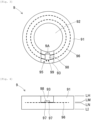
- annular sensor 9 As an example of molded object Fr, a configuration of annular sensor 9 for detecting a magnetic field and a method of manufacturing the same will be described. As shown in Fig. 3 and Fig. 4 , annular sensor 9 includes annular base portion 91 having hollow portion 92, and electronic circuit 95 included in base portion 91. A cross-section orthogonal to a circumferential direction of base portion 91 is rectangular, but the cross-section may be circular without limitation. A portion of the circumferential direction of base portion 91 has a thickness of approximately an upper half thereof omitted to form a circuit exposed portion 93.
- Circuit 95 is configured by circuit pattern 96 and two electronic components connected to circuit pattern 96.
- Circuit pattern 96 is buried in an intermediate height of base portion 91 and is exposed in circuit exposed portion 93.
- Circuit pattern 96 is formed of two concentric circular wires along the circumferential direction of base portion 91. Strictly speaking, circuit pattern 96 includes two arcuate wires having a center angle slightly smaller than 360°, and having both ends at the position of circuit exposed portion 93. A total of four end portions of circuit pattern 96 constitute component mounting position 97.
- the electronic component includes detection component 98 and battery 9A.
- Detection component 98 is connected to an upper side of four component mounting positions 97 of circuit pattern 96. Detection component 98 detects a magnitude of a magnetic field linked to annular circuit pattern 96 using electromagnetic induction action. Detection component 98 has a rectangular plate-like outer shape and has pair of output terminals 99. By disposing detection component 98 in circuit exposed portion 93, an output signal of output terminal 99 can be extracted to the outside using an output line.
- Battery 9A is mounted at a position closer to detection component 98. Battery 9A is directly connected to a power supply terminal (not shown) of detection component 98 to supply power to detection component 98. Battery 9A is disposed in circuit exposed portion 93 so as to be exchangeable at the time of consumption. Detection component 98 and battery 9A are supplied from component tray Ty on component pallet Pp.
- detection component 98 is held in twenty component trays Ty on component pallet Pp, and battery 9A is held in other twenty component trays Ty.
- feeder-type component supplying unit 45 is placed in a halt state.
- frequency of component shortage is low. In other words, the frequency of -out and re--in of component pallet Pp is low.
- the tray-type component supplying device having a conventional configuration raises or lowers and selects component tray Ty holding detection component 98 and component tray Ty holding battery 9A, and pulls out one component tray Ty to a component supplying position to perform a component supply action. Therefore, it is necessary to replace component tray Ty pulled out for each molding pallet Pm, and thus, the production efficiency is low.
- the conventional configuration when the number of types of electronic components to be supplied using component tray Ty is further increased, the decrease in the production efficiency becomes more remarkable.
- component conveyance device 6 uses component pallet Pp for supplying multiple types of electronic components, the frequency of replacement of component tray Ty is reduced, and thus, the production efficiency is enhanced.
- configuration of component conveyance device 6 is simplified as compared with the case where a raising/lowering mechanism and a pull-out mechanism are required in the conventional configuration, it is also advantageous in terms of facility cost.
- the control device holds three-dimensional shape data of annular sensor 9.
- the three-dimensional shape data includes lowermost first layer data L1 to uppermost layer data LH located on the uppermost side shown in Fig. 4 .
- descriptions will be made in order from the lower layer data.
- First layer data L1 to (N-1)th layer data are the same as each other and represent a planar cross-sectional shape of an annular shape that does not include circuit exposed portion 93 of base portion 91.
- Nth layer data LN to (M-1)th layer data are the same as each other and represent the C-shaped horizontal cross-sectional shape that circuit exposed portion 93 of base portion 91 has, and the shape of circuit pattern 96 to be embedded.
- Mth layer data LM represents component mounting position 97 at which detection component 98 and battery 9A are mounted, in addition to the C-shaped horizontal cross-sectional shape that circuit exposed portion 93 of base portion 91 has.
- (M+1)th layer data to uppermost layer data LH are the same as each other and represent a C-shaped horizontal cross-sectional shape that circuit exposed portion 93 of base portion 91 has.
- first step P1 pallet conveyance device 5 conveys in molding pallet Pm from - in end 53.
- the control device controls so as to repeat second step P2 to fifth step P5 for each layer data, referring to the lower layer data in order. It should be noted that not all of second step P2, third step P3, and fourth step P4 are executed in the repetition. Actually, either one step only or two steps are often executed.
- next fifth step P5 the control device determines whether the control for referring to uppermost layer data LH is finished. When not finished, the control device advances the layer data to be referenced to the upper side by one, and returns the execution of the control to second step P2. When the control for referring to uppermost layer data LH is finished and the manufacture of annular sensor 9 is finished, the control device advances the execution of the control to sixth step P6.
- sixth step P6 pallet conveyance device 5 carries out annular sensor 9 together with molding pallet Pm from convey-out end 54. This completes one cycle of manufacturing annular sensor 9.
- the second step and the fourth step are executed.
- detection component 98 and battery 9A are mounted on component mounting position 97 on circuit pattern 96 (refer to Fig. 7 ).
- only the second step is repeatedly executed while (M+1)th layer data to uppermost layer data LH are referenced.
- (M+1)th layer data to uppermost layer data LH are referenced.
- a substantially upper half of base portion 91 including circuit exposed portion 93 is molded, and thus, circuit pattern 96 is embedded.
- the molding of the molded object (annular sensor 9), the formation of circuit pattern 96, and the mounting of the electronic components (detection component 98 and battery 9A) are performed by each device (2, 3, 4) in the machine, and the conveyance of the molded object between the devices and the -in of the electronic components from the outside of the machine are performed using the two sets of conveyance devices (5, 6). Accordingly, it is possible to manufacture the molded object including electronic circuit 95 with high production efficiency without requiring a great deal of effort.
- component mounting machine 8 (refer to Fig. 1 ) can be configured by combining left-right conveyance unit 51, component conveyance device 6, and component mounting device 4.
- Component mounting machine 8 is incorporated in three-dimensional molding machine 1, or is configured separately from three-dimensional molding machine 1.
- Separate component mounting machine 8 may be a mounting target object such as a thin plate-shaped substrate on which a circuit pattern is formed, in addition to the above-described molded object.
- Separate component mounting machine 8 includes left-right conveyance unit 51 serving as the target object conveyance device configured to in and out the mounting target object on which a circuit pattern is formed, component conveyance device 6 configured to in component pallet Pp on which multiple component trays Ty configured to hold multiple types of electronic components for each type are placed, and component mounting device 4 serving as component transferring device configured to collect electronic components from component tray Ty conveyed in by component conveyance device 6 and mount the electronic components on the circuit pattern of the mounting target object conveyed in by the target object conveyance device.
- component pallet Pp on which multiple component trays Ty for holding multiple types of electronic components for each type are placed is used. Therefore, the replacement of component tray Ty or component pallet Pp may be performed only when the component runs out, and thus, multiple types of electronic components can be efficiently supplied from one component pallet Pp.
- three-dimensional molding machine 1 is configured by integrating molding block 1R and mounting block 1L, but is not limited to this.
- pallet conveyance device 5 can be configured to be linear by arranging three-dimensional molding device 2, circuit forming device 3, and component mounting device 4 in a row.
- the internal arrangement of the constituent elements constituting each of three-dimensional molding device 2, circuit forming device 3, and component mounting device 4 can be appropriately changed.
- the molding by three-dimensional molding device 2 may be performed by a method or a raw material other than those described in the embodiment.
- Circuit forming device 3 may use a forming method other than the drawing operation by drawing head 32 and inkjet nozzle 33.
Landscapes
- Engineering & Computer Science (AREA)
- Manufacturing & Machinery (AREA)
- Microelectronics & Electronic Packaging (AREA)
- Chemical & Material Sciences (AREA)
- Materials Engineering (AREA)
- Physics & Mathematics (AREA)
- Mechanical Engineering (AREA)
- Optics & Photonics (AREA)
- Supply And Installment Of Electrical Components (AREA)
- Electric Connection Of Electric Components To Printed Circuits (AREA)
- Manufacturing Of Printed Wiring (AREA)
Claims (7)
- Machine de moulage tridimensionnel (1) comprenant :un dispositif de moulage tridimensionnel (2) configuré pour mouler un objet tridimensionnel (Fr) sur une palette de moulage (Pm) ;un dispositif de formation de circuit (3) configuré pour former un schéma de circuit (96) sur l'objet moulé (Fr) pendant ou après un moulage ;dispositif de montage de composant (4) configuré pour monter un composant électronique sur le schéma de circuit (96) formé sur l'objet moulé (Fr) ;un dispositif de convoyage de palette (5) configuré pour convoyer l'objet moulé (Fr) conjointement avec la palette de moulage (Pm) entre le dispositif de moulage tridimensionnel (2),le dispositif de formation de circuit (3) et le dispositif de montage de composant (4) ; etun dispositif de convoyage de composants (6) configuré pour convoyer les composants électroniques dans le dispositif de montage de composant (4) depuis un extérieur de la machine (1)caractérisée en ce que :la machine de moulage tridimensionnel (1) est configurée en intégrant un bloc de moulage (1R) et un bloc de montage (1L) sur deux côtés différents, dans laquellele dispositif de convoyage de palette (5) est disposé dans le bloc de moulage (1R), dans laquellele dispositif de convoyage de composants (6) est disposé sur une position en avant du dispositif de convoyage de palette (5) dans le bloc de montage (1L) de sorte à être parallèle à celui-ci.
- La machine de moulage tridimensionnel (1) selon la revendication 1, dans laquelle
le dispositif de convoyage de composants (6) est configuré pour convoyer sur une palette de composants (Pp) sur laquelle sont placés plusieurs plateaux de composants (Ty) configurés pour contenir plusieurs types des composants électroniques pour chaque type. - La machine de moulage tridimensionnel (1) selon la revendication 1 ou 2, dans laquelle
le dispositif de convoyage de palette (5) est configuré pour convoyer la palette de moulage (Pm) jusque dans la machine (1) et convoie la palette de moulage (Pm) vers un extérieur de la machine (1). - La machine de moulage tridimensionnel (1) selon l'une quelconque des revendications 1 à 3, dans laquelle
chacun du dispositif de convoyage de palette (5) et du dispositif de convoyage de composants (6) est un dispositif de convoyeur présentant une courroie de convoyeur qui tourne. - La machine de moulage tridimensionnel (1) selon l'une quelconque des revendications 1 à 4, dans laquelle
le dispositif de formation de circuit (3) est un dispositif de dessin configuré pour dessiner le schéma de circuit (96) sur l'objet moulé (Fr) au moyen d'une encre conductrice. - La machine de moulage tridimensionnel (1) selon l'une quelconque des revendications 1 à 5, dans laquellele dispositif de montage de composants (4) inclutune tête de montage (42) configurée pour maintenir de manière échangeable un applicateur (44) configuré pour appliquer un matériau conducteur sous forme de pâte sur une position de montage de composant (97) du schéma de circuit (96), et un outil de montage de composant (43) qui est configuré pour collecter le composant électronique et monte le composant électronique sur le matériau conducteur enduit, ouune tête de montage (42) configurée pour maintenir à la fois l'applicateur (44) et l'outil de montage de composant (43).
- La machine de moulage tridimensionnel (1) selon l'une quelconque des revendications 1 à 6, dans laquellele dispositif de montage de composant (4), le dispositif de convoyage de palette (5) et le dispositif de convoyage de composants (6) forment une machine de montage de composants (8), dans laquellela machine de montage de composants (8) est intégrée à la machine de moulage tridimensionnel (1) ou est configurée séparément de la machine de moulage tridimensionnel (1).
Applications Claiming Priority (1)
| Application Number | Priority Date | Filing Date | Title |
|---|---|---|---|
| PCT/JP2019/027961 WO2021009854A1 (fr) | 2019-07-16 | 2019-07-16 | Machine de moulage tridimensionnel et machine de montage de composant |
Publications (3)
| Publication Number | Publication Date |
|---|---|
| EP4002962A1 EP4002962A1 (fr) | 2022-05-25 |
| EP4002962A4 EP4002962A4 (fr) | 2022-07-20 |
| EP4002962B1 true EP4002962B1 (fr) | 2024-08-28 |
Family
ID=74209740
Family Applications (2)
| Application Number | Title | Priority Date | Filing Date |
|---|---|---|---|
| EP19937697.1A Active EP4002962B1 (fr) | 2019-07-16 | 2019-07-16 | Machine de moulage tridimensionnel et machine de montage de composant |
| EP19937374.7A Pending EP4000930A4 (fr) | 2019-07-16 | 2019-11-13 | Machine de moulage en trois dimensions |
Family Applications After (1)
| Application Number | Title | Priority Date | Filing Date |
|---|---|---|---|
| EP19937374.7A Pending EP4000930A4 (fr) | 2019-07-16 | 2019-11-13 | Machine de moulage en trois dimensions |
Country Status (4)
| Country | Link |
|---|---|
| US (2) | US12520464B2 (fr) |
| EP (2) | EP4002962B1 (fr) |
| JP (2) | JP7434323B2 (fr) |
| WO (2) | WO2021009854A1 (fr) |
Families Citing this family (3)
| Publication number | Priority date | Publication date | Assignee | Title |
|---|---|---|---|---|
| US11943871B2 (en) * | 2019-02-14 | 2024-03-26 | Fuji Corporation | Component mounter |
| WO2021009854A1 (fr) * | 2019-07-16 | 2021-01-21 | 株式会社Fuji | Machine de moulage tridimensionnel et machine de montage de composant |
| CN112959664A (zh) * | 2021-02-01 | 2021-06-15 | 江西炫智教育科技有限公司 | 一种针对双头三维打印机的溶解取模辅助装置 |
Family Cites Families (29)
| Publication number | Priority date | Publication date | Assignee | Title |
|---|---|---|---|---|
| JPS5869658A (ja) | 1981-10-15 | 1983-04-25 | Dainippon Printing Co Ltd | 枚葉紙の矯正装置 |
| US6572702B1 (en) | 1999-12-21 | 2003-06-03 | Speedline Technologies, Inc. | High speed electronic assembly system and method |
| JP2005322702A (ja) | 2004-05-07 | 2005-11-17 | Matsushita Electric Ind Co Ltd | メンテナンス装置 |
| JP2006066811A (ja) * | 2004-08-30 | 2006-03-09 | Toshiba Corp | はんだ印刷用マスク、部品実装方法 |
| JP5008579B2 (ja) | 2008-01-29 | 2012-08-22 | 富士機械製造株式会社 | 電子部品の実装方法、装置及びライン |
| JP4883071B2 (ja) * | 2008-10-03 | 2012-02-22 | パナソニック株式会社 | 電子部品実装システム |
| JP2010147267A (ja) * | 2008-12-19 | 2010-07-01 | Renesas Technology Corp | 半導体集積回路装置および半導体集積回路装置の製造方法 |
| US8419404B2 (en) * | 2010-02-05 | 2013-04-16 | Asm Technology Singapore Pte Ltd | Modular molding assembly for electronic devices |
| JP5675013B2 (ja) * | 2010-06-10 | 2015-02-25 | 富士機械製造株式会社 | 電子回路組立方法および電子回路組立システム |
| JP5843551B2 (ja) | 2011-09-30 | 2016-01-13 | 富士機械製造株式会社 | マルチディスペンサ装置 |
| JP6111092B2 (ja) | 2013-03-06 | 2017-04-05 | ヤマハ発動機株式会社 | 電子部品実装装置の部品供給方法および電子部品実装装置用部品供給装置 |
| JP2015084388A (ja) | 2013-10-25 | 2015-04-30 | シャープ株式会社 | 搭載部品収納治具、マルチ部品実装装置およびマルチ部品実装方法 |
| JP6272346B2 (ja) | 2013-11-07 | 2018-01-31 | 富士機械製造株式会社 | 対基板作業装置および対基板作業ライン |
| US10645812B2 (en) | 2014-04-21 | 2020-05-05 | Cornell University | System and methods for additive manufacturing of electromechanical assemblies |
| US10667403B2 (en) | 2014-09-19 | 2020-05-26 | Fuji Corporation | Manufacturing apparatus for performing additive manufacturing of an electrical device |
| JP2017101933A (ja) | 2015-11-30 | 2017-06-08 | セイコーエプソン株式会社 | 電子部品搬送装置および電子部品検査装置 |
| JP6512448B2 (ja) | 2015-11-30 | 2019-05-15 | 清水建設株式会社 | 建物の応答推定方法 |
| JP2017130553A (ja) * | 2016-01-20 | 2017-07-27 | 株式会社ミマキエンジニアリング | 電子素子設置基材の製造方法、電子部材の製造方法、及び造形装置 |
| JP6762968B2 (ja) * | 2016-02-17 | 2020-09-30 | 株式会社Fuji | 作業装置および生産ライン |
| DE102016104677A1 (de) | 2016-03-14 | 2017-09-14 | Cl Schutzrechtsverwaltungs Gmbh | Anlage zur additiven Herstellung dreidimensionaler Objekte |
| DE102016221821A1 (de) | 2016-11-08 | 2018-05-09 | Robert Bosch Gmbh | Verfahren und Vorrichtung zur additiven Fertigung eines dreidimensionalen Werkstücks |
| WO2018134873A1 (fr) | 2017-01-17 | 2018-07-26 | ヤマハ発動機株式会社 | Dispositif de travail pour support |
| JP6677183B2 (ja) * | 2017-01-25 | 2020-04-08 | オムロン株式会社 | 制御装置 |
| JP2018182050A (ja) | 2017-04-12 | 2018-11-15 | 株式会社村田製作所 | 回路基板の製造方法、および、回路基板 |
| WO2019102522A1 (fr) | 2017-11-21 | 2019-05-31 | 株式会社Fuji | Procédé de production de dispositif électronique multicouche tridimensionnel, et dispositif électronique multicouche tridimensionnel |
| JP6971142B2 (ja) * | 2017-12-20 | 2021-11-24 | 株式会社Fuji | 基板生産ラインおよび情報管理装置 |
| JP7055014B2 (ja) | 2017-12-26 | 2022-04-15 | 前田建設工業株式会社 | 積層複合構造物の造形装置及び造形方法 |
| US11090724B2 (en) | 2017-12-28 | 2021-08-17 | Applied Materials, Inc. | Additive manufacturing with powder dispensing |
| WO2021009854A1 (fr) * | 2019-07-16 | 2021-01-21 | 株式会社Fuji | Machine de moulage tridimensionnel et machine de montage de composant |
-
2019
- 2019-07-16 WO PCT/JP2019/027961 patent/WO2021009854A1/fr not_active Ceased
- 2019-07-16 US US17/627,072 patent/US12520464B2/en active Active
- 2019-07-16 EP EP19937697.1A patent/EP4002962B1/fr active Active
- 2019-07-16 JP JP2021532606A patent/JP7434323B2/ja active Active
- 2019-11-13 EP EP19937374.7A patent/EP4000930A4/fr active Pending
- 2019-11-13 WO PCT/JP2019/044592 patent/WO2021009940A1/fr not_active Ceased
- 2019-11-13 JP JP2021532666A patent/JP7309878B2/ja active Active
- 2019-11-13 US US17/626,430 patent/US12245378B2/en active Active
Also Published As
| Publication number | Publication date |
|---|---|
| US12245378B2 (en) | 2025-03-04 |
| EP4000930A4 (fr) | 2022-09-14 |
| WO2021009854A1 (fr) | 2021-01-21 |
| JPWO2021009854A1 (fr) | 2021-01-21 |
| EP4002962A4 (fr) | 2022-07-20 |
| EP4002962A1 (fr) | 2022-05-25 |
| US20220274336A1 (en) | 2022-09-01 |
| JPWO2021009940A1 (fr) | 2021-01-21 |
| WO2021009940A1 (fr) | 2021-01-21 |
| US20220264777A1 (en) | 2022-08-18 |
| JP7434323B2 (ja) | 2024-02-20 |
| US12520464B2 (en) | 2026-01-06 |
| JP7309878B2 (ja) | 2023-07-18 |
| EP4000930A1 (fr) | 2022-05-25 |
Similar Documents
| Publication | Publication Date | Title |
|---|---|---|
| US11470724B2 (en) | Manufacturing apparatus for performing additive manufacturing of an electrical device | |
| CN102132641B (zh) | 电子元件安装系统 | |
| EP4002962B1 (fr) | Machine de moulage tridimensionnel et machine de montage de composant | |
| JP4883071B2 (ja) | 電子部品実装システム | |
| JP4883070B2 (ja) | 電子部品実装システムおよび電子部品実装方法 | |
| CN1918954B (zh) | 模板检查和清理同时进行的方法和装置 | |
| JP4883069B2 (ja) | 電子部品実装システムおよび電子部品実装方法 | |
| CN101740418A (zh) | 元件安装设备和元件安装方法 | |
| KR20010090483A (ko) | 부품 장착 장치 | |
| WO2004053301A2 (fr) | Systeme et procede de distribution | |
| JP5473465B2 (ja) | 電子部品の実装装置 | |
| JP7175869B2 (ja) | 樹脂成形装置および樹脂成形方法 | |
| CN103608909B (zh) | 基板搬运方法及基板搬运装置 | |
| CN1738695A (zh) | 分配系统和方法 |
Legal Events
| Date | Code | Title | Description |
|---|---|---|---|
| STAA | Information on the status of an ep patent application or granted ep patent |
Free format text: STATUS: THE INTERNATIONAL PUBLICATION HAS BEEN MADE |
|
| PUAI | Public reference made under article 153(3) epc to a published international application that has entered the european phase |
Free format text: ORIGINAL CODE: 0009012 |
|
| STAA | Information on the status of an ep patent application or granted ep patent |
Free format text: STATUS: REQUEST FOR EXAMINATION WAS MADE |
|
| 17P | Request for examination filed |
Effective date: 20220111 |
|
| AK | Designated contracting states |
Kind code of ref document: A1 Designated state(s): AL AT BE BG CH CY CZ DE DK EE ES FI FR GB GR HR HU IE IS IT LI LT LU LV MC MK MT NL NO PL PT RO RS SE SI SK SM TR |
|
| REG | Reference to a national code |
Ref country code: DE Ref legal event code: R079 Free format text: PREVIOUS MAIN CLASS: H05K0003000000 Ipc: H05K0013040000 Ref country code: DE Ref legal event code: R079 Ref document number: 602019058130 Country of ref document: DE Free format text: PREVIOUS MAIN CLASS: H05K0003000000 Ipc: H05K0013040000 |
|
| A4 | Supplementary search report drawn up and despatched |
Effective date: 20220620 |
|
| RIC1 | Information provided on ipc code assigned before grant |
Ipc: B29L 31/34 20060101ALI20220614BHEP Ipc: B33Y 40/00 20200101ALI20220614BHEP Ipc: B33Y 30/00 20150101ALI20220614BHEP Ipc: B29C 64/30 20170101ALI20220614BHEP Ipc: B29C 64/112 20170101ALI20220614BHEP Ipc: H05K 13/02 20060101ALI20220614BHEP Ipc: H05K 3/00 20060101ALI20220614BHEP Ipc: H05K 13/04 20060101AFI20220614BHEP |
|
| DAV | Request for validation of the european patent (deleted) | ||
| DAX | Request for extension of the european patent (deleted) | ||
| P01 | Opt-out of the competence of the unified patent court (upc) registered |
Effective date: 20230328 |
|
| STAA | Information on the status of an ep patent application or granted ep patent |
Free format text: STATUS: EXAMINATION IS IN PROGRESS |
|
| 17Q | First examination report despatched |
Effective date: 20231127 |
|
| GRAP | Despatch of communication of intention to grant a patent |
Free format text: ORIGINAL CODE: EPIDOSNIGR1 |
|
| STAA | Information on the status of an ep patent application or granted ep patent |
Free format text: STATUS: GRANT OF PATENT IS INTENDED |
|
| RIC1 | Information provided on ipc code assigned before grant |
Ipc: H05K 3/12 20060101ALI20240508BHEP Ipc: H05K 1/18 20060101ALI20240508BHEP Ipc: H05K 1/09 20060101ALI20240508BHEP Ipc: H05K 1/02 20060101ALI20240508BHEP Ipc: B29L 31/34 20060101ALI20240508BHEP Ipc: B33Y 40/00 20200101ALI20240508BHEP Ipc: B33Y 30/00 20150101ALI20240508BHEP Ipc: B29C 64/30 20170101ALI20240508BHEP Ipc: B29C 64/112 20170101ALI20240508BHEP Ipc: H05K 13/02 20060101ALI20240508BHEP Ipc: H05K 3/00 20060101ALI20240508BHEP Ipc: H05K 13/04 20060101AFI20240508BHEP |
|
| INTG | Intention to grant announced |
Effective date: 20240529 |
|
| GRAS | Grant fee paid |
Free format text: ORIGINAL CODE: EPIDOSNIGR3 |
|
| GRAA | (expected) grant |
Free format text: ORIGINAL CODE: 0009210 |
|
| STAA | Information on the status of an ep patent application or granted ep patent |
Free format text: STATUS: THE PATENT HAS BEEN GRANTED |
|
| AK | Designated contracting states |
Kind code of ref document: B1 Designated state(s): AL AT BE BG CH CY CZ DE DK EE ES FI FR GB GR HR HU IE IS IT LI LT LU LV MC MK MT NL NO PL PT RO RS SE SI SK SM TR |
|
| REG | Reference to a national code |
Ref country code: CH Ref legal event code: EP |
|
| REG | Reference to a national code |
Ref country code: DE Ref legal event code: R096 Ref document number: 602019058130 Country of ref document: DE |
|
| REG | Reference to a national code |
Ref country code: IE Ref legal event code: FG4D |
|
| REG | Reference to a national code |
Ref country code: LT Ref legal event code: MG9D |
|
| PG25 | Lapsed in a contracting state [announced via postgrant information from national office to epo] |
Ref country code: NO Free format text: LAPSE BECAUSE OF FAILURE TO SUBMIT A TRANSLATION OF THE DESCRIPTION OR TO PAY THE FEE WITHIN THE PRESCRIBED TIME-LIMIT Effective date: 20241128 |
|
| REG | Reference to a national code |
Ref country code: AT Ref legal event code: MK05 Ref document number: 1719328 Country of ref document: AT Kind code of ref document: T Effective date: 20240828 |
|
| PG25 | Lapsed in a contracting state [announced via postgrant information from national office to epo] |
Ref country code: NL Free format text: LAPSE BECAUSE OF FAILURE TO SUBMIT A TRANSLATION OF THE DESCRIPTION OR TO PAY THE FEE WITHIN THE PRESCRIBED TIME-LIMIT Effective date: 20240828 Ref country code: PT Free format text: LAPSE BECAUSE OF FAILURE TO SUBMIT A TRANSLATION OF THE DESCRIPTION OR TO PAY THE FEE WITHIN THE PRESCRIBED TIME-LIMIT Effective date: 20241230 Ref country code: PL Free format text: LAPSE BECAUSE OF FAILURE TO SUBMIT A TRANSLATION OF THE DESCRIPTION OR TO PAY THE FEE WITHIN THE PRESCRIBED TIME-LIMIT Effective date: 20240828 Ref country code: FI Free format text: LAPSE BECAUSE OF FAILURE TO SUBMIT A TRANSLATION OF THE DESCRIPTION OR TO PAY THE FEE WITHIN THE PRESCRIBED TIME-LIMIT Effective date: 20240828 Ref country code: GR Free format text: LAPSE BECAUSE OF FAILURE TO SUBMIT A TRANSLATION OF THE DESCRIPTION OR TO PAY THE FEE WITHIN THE PRESCRIBED TIME-LIMIT Effective date: 20241129 |
|
| PG25 | Lapsed in a contracting state [announced via postgrant information from national office to epo] |
Ref country code: BG Free format text: LAPSE BECAUSE OF FAILURE TO SUBMIT A TRANSLATION OF THE DESCRIPTION OR TO PAY THE FEE WITHIN THE PRESCRIBED TIME-LIMIT Effective date: 20240828 |
|
| PG25 | Lapsed in a contracting state [announced via postgrant information from national office to epo] |
Ref country code: LV Free format text: LAPSE BECAUSE OF FAILURE TO SUBMIT A TRANSLATION OF THE DESCRIPTION OR TO PAY THE FEE WITHIN THE PRESCRIBED TIME-LIMIT Effective date: 20240828 |
|
| REG | Reference to a national code |
Ref country code: NL Ref legal event code: MP Effective date: 20240828 |
|
| PG25 | Lapsed in a contracting state [announced via postgrant information from national office to epo] |
Ref country code: IS Free format text: LAPSE BECAUSE OF FAILURE TO SUBMIT A TRANSLATION OF THE DESCRIPTION OR TO PAY THE FEE WITHIN THE PRESCRIBED TIME-LIMIT Effective date: 20241228 Ref country code: AT Free format text: LAPSE BECAUSE OF FAILURE TO SUBMIT A TRANSLATION OF THE DESCRIPTION OR TO PAY THE FEE WITHIN THE PRESCRIBED TIME-LIMIT Effective date: 20240828 |
|
| PG25 | Lapsed in a contracting state [announced via postgrant information from national office to epo] |
Ref country code: HR Free format text: LAPSE BECAUSE OF FAILURE TO SUBMIT A TRANSLATION OF THE DESCRIPTION OR TO PAY THE FEE WITHIN THE PRESCRIBED TIME-LIMIT Effective date: 20240828 |
|
| PG25 | Lapsed in a contracting state [announced via postgrant information from national office to epo] |
Ref country code: RS Free format text: LAPSE BECAUSE OF FAILURE TO SUBMIT A TRANSLATION OF THE DESCRIPTION OR TO PAY THE FEE WITHIN THE PRESCRIBED TIME-LIMIT Effective date: 20241128 Ref country code: ES Free format text: LAPSE BECAUSE OF FAILURE TO SUBMIT A TRANSLATION OF THE DESCRIPTION OR TO PAY THE FEE WITHIN THE PRESCRIBED TIME-LIMIT Effective date: 20240828 |
|
| PG25 | Lapsed in a contracting state [announced via postgrant information from national office to epo] |
Ref country code: RS Free format text: LAPSE BECAUSE OF FAILURE TO SUBMIT A TRANSLATION OF THE DESCRIPTION OR TO PAY THE FEE WITHIN THE PRESCRIBED TIME-LIMIT Effective date: 20241128 Ref country code: PT Free format text: LAPSE BECAUSE OF FAILURE TO SUBMIT A TRANSLATION OF THE DESCRIPTION OR TO PAY THE FEE WITHIN THE PRESCRIBED TIME-LIMIT Effective date: 20241230 Ref country code: PL Free format text: LAPSE BECAUSE OF FAILURE TO SUBMIT A TRANSLATION OF THE DESCRIPTION OR TO PAY THE FEE WITHIN THE PRESCRIBED TIME-LIMIT Effective date: 20240828 Ref country code: NO Free format text: LAPSE BECAUSE OF FAILURE TO SUBMIT A TRANSLATION OF THE DESCRIPTION OR TO PAY THE FEE WITHIN THE PRESCRIBED TIME-LIMIT Effective date: 20241128 Ref country code: NL Free format text: LAPSE BECAUSE OF FAILURE TO SUBMIT A TRANSLATION OF THE DESCRIPTION OR TO PAY THE FEE WITHIN THE PRESCRIBED TIME-LIMIT Effective date: 20240828 Ref country code: LV Free format text: LAPSE BECAUSE OF FAILURE TO SUBMIT A TRANSLATION OF THE DESCRIPTION OR TO PAY THE FEE WITHIN THE PRESCRIBED TIME-LIMIT Effective date: 20240828 Ref country code: IS Free format text: LAPSE BECAUSE OF FAILURE TO SUBMIT A TRANSLATION OF THE DESCRIPTION OR TO PAY THE FEE WITHIN THE PRESCRIBED TIME-LIMIT Effective date: 20241228 Ref country code: HR Free format text: LAPSE BECAUSE OF FAILURE TO SUBMIT A TRANSLATION OF THE DESCRIPTION OR TO PAY THE FEE WITHIN THE PRESCRIBED TIME-LIMIT Effective date: 20240828 Ref country code: GR Free format text: LAPSE BECAUSE OF FAILURE TO SUBMIT A TRANSLATION OF THE DESCRIPTION OR TO PAY THE FEE WITHIN THE PRESCRIBED TIME-LIMIT Effective date: 20241129 Ref country code: FI Free format text: LAPSE BECAUSE OF FAILURE TO SUBMIT A TRANSLATION OF THE DESCRIPTION OR TO PAY THE FEE WITHIN THE PRESCRIBED TIME-LIMIT Effective date: 20240828 Ref country code: ES Free format text: LAPSE BECAUSE OF FAILURE TO SUBMIT A TRANSLATION OF THE DESCRIPTION OR TO PAY THE FEE WITHIN THE PRESCRIBED TIME-LIMIT Effective date: 20240828 Ref country code: BG Free format text: LAPSE BECAUSE OF FAILURE TO SUBMIT A TRANSLATION OF THE DESCRIPTION OR TO PAY THE FEE WITHIN THE PRESCRIBED TIME-LIMIT Effective date: 20240828 Ref country code: AT Free format text: LAPSE BECAUSE OF FAILURE TO SUBMIT A TRANSLATION OF THE DESCRIPTION OR TO PAY THE FEE WITHIN THE PRESCRIBED TIME-LIMIT Effective date: 20240828 |
|
| PG25 | Lapsed in a contracting state [announced via postgrant information from national office to epo] |
Ref country code: SM Free format text: LAPSE BECAUSE OF FAILURE TO SUBMIT A TRANSLATION OF THE DESCRIPTION OR TO PAY THE FEE WITHIN THE PRESCRIBED TIME-LIMIT Effective date: 20240828 Ref country code: RO Free format text: LAPSE BECAUSE OF FAILURE TO SUBMIT A TRANSLATION OF THE DESCRIPTION OR TO PAY THE FEE WITHIN THE PRESCRIBED TIME-LIMIT Effective date: 20240828 Ref country code: DK Free format text: LAPSE BECAUSE OF FAILURE TO SUBMIT A TRANSLATION OF THE DESCRIPTION OR TO PAY THE FEE WITHIN THE PRESCRIBED TIME-LIMIT Effective date: 20240828 |
|
| PG25 | Lapsed in a contracting state [announced via postgrant information from national office to epo] |
Ref country code: EE Free format text: LAPSE BECAUSE OF FAILURE TO SUBMIT A TRANSLATION OF THE DESCRIPTION OR TO PAY THE FEE WITHIN THE PRESCRIBED TIME-LIMIT Effective date: 20240828 |
|
| PG25 | Lapsed in a contracting state [announced via postgrant information from national office to epo] |
Ref country code: CZ Free format text: LAPSE BECAUSE OF FAILURE TO SUBMIT A TRANSLATION OF THE DESCRIPTION OR TO PAY THE FEE WITHIN THE PRESCRIBED TIME-LIMIT Effective date: 20240828 |
|
| PG25 | Lapsed in a contracting state [announced via postgrant information from national office to epo] |
Ref country code: IT Free format text: LAPSE BECAUSE OF FAILURE TO SUBMIT A TRANSLATION OF THE DESCRIPTION OR TO PAY THE FEE WITHIN THE PRESCRIBED TIME-LIMIT Effective date: 20240828 Ref country code: SK Free format text: LAPSE BECAUSE OF FAILURE TO SUBMIT A TRANSLATION OF THE DESCRIPTION OR TO PAY THE FEE WITHIN THE PRESCRIBED TIME-LIMIT Effective date: 20240828 |
|
| REG | Reference to a national code |
Ref country code: DE Ref legal event code: R097 Ref document number: 602019058130 Country of ref document: DE |
|
| PLBE | No opposition filed within time limit |
Free format text: ORIGINAL CODE: 0009261 |
|
| STAA | Information on the status of an ep patent application or granted ep patent |
Free format text: STATUS: NO OPPOSITION FILED WITHIN TIME LIMIT |
|
| PGFP | Annual fee paid to national office [announced via postgrant information from national office to epo] |
Ref country code: FR Payment date: 20250610 Year of fee payment: 7 |
|
| 26N | No opposition filed |
Effective date: 20250530 |
|
| PG25 | Lapsed in a contracting state [announced via postgrant information from national office to epo] |
Ref country code: SE Free format text: LAPSE BECAUSE OF FAILURE TO SUBMIT A TRANSLATION OF THE DESCRIPTION OR TO PAY THE FEE WITHIN THE PRESCRIBED TIME-LIMIT Effective date: 20240828 |
|
| PGFP | Annual fee paid to national office [announced via postgrant information from national office to epo] |
Ref country code: DE Payment date: 20250528 Year of fee payment: 7 |
|
| REG | Reference to a national code |
Ref country code: CH Ref legal event code: H13 Free format text: ST27 STATUS EVENT CODE: U-0-0-H10-H13 (AS PROVIDED BY THE NATIONAL OFFICE) Effective date: 20260224 |
|
| PG25 | Lapsed in a contracting state [announced via postgrant information from national office to epo] |
Ref country code: LU Free format text: LAPSE BECAUSE OF NON-PAYMENT OF DUE FEES Effective date: 20250716 |
|
| GBPC | Gb: european patent ceased through non-payment of renewal fee |
Effective date: 20250716 |
|
| REG | Reference to a national code |
Ref country code: BE Ref legal event code: MM Effective date: 20250731 |
|
| PG25 | Lapsed in a contracting state [announced via postgrant information from national office to epo] |
Ref country code: GB Free format text: LAPSE BECAUSE OF NON-PAYMENT OF DUE FEES Effective date: 20250716 |
|
| PG25 | Lapsed in a contracting state [announced via postgrant information from national office to epo] |
Ref country code: BE Free format text: LAPSE BECAUSE OF NON-PAYMENT OF DUE FEES Effective date: 20250731 |
|
| PG25 | Lapsed in a contracting state [announced via postgrant information from national office to epo] |
Ref country code: CH Free format text: LAPSE BECAUSE OF NON-PAYMENT OF DUE FEES Effective date: 20250731 |