EP4004486B1 - Dispositif et procédé de mesure de profils de hauteur sur un objet - Google Patents
Dispositif et procédé de mesure de profils de hauteur sur un objet Download PDFInfo
- Publication number
- EP4004486B1 EP4004486B1 EP20740328.8A EP20740328A EP4004486B1 EP 4004486 B1 EP4004486 B1 EP 4004486B1 EP 20740328 A EP20740328 A EP 20740328A EP 4004486 B1 EP4004486 B1 EP 4004486B1
- Authority
- EP
- European Patent Office
- Prior art keywords
- beams
- mirror
- light
- evaluation
- reflection
- Prior art date
- Legal status (The legal status is an assumption and is not a legal conclusion. Google has not performed a legal analysis and makes no representation as to the accuracy of the status listed.)
- Active
Links
Images


Classifications
-
- G—PHYSICS
- G01—MEASURING; TESTING
- G01B—MEASURING LENGTH, THICKNESS OR SIMILAR LINEAR DIMENSIONS; MEASURING ANGLES; MEASURING AREAS; MEASURING IRREGULARITIES OF SURFACES OR CONTOURS
- G01B11/00—Measuring arrangements characterised by the use of optical techniques
- G01B11/02—Measuring arrangements characterised by the use of optical techniques for measuring length, width or thickness
- G01B11/06—Measuring arrangements characterised by the use of optical techniques for measuring length, width or thickness for measuring thickness ; e.g. of sheet material
- G01B11/0608—Height gauges
-
- G—PHYSICS
- G01—MEASURING; TESTING
- G01B—MEASURING LENGTH, THICKNESS OR SIMILAR LINEAR DIMENSIONS; MEASURING ANGLES; MEASURING AREAS; MEASURING IRREGULARITIES OF SURFACES OR CONTOURS
- G01B11/00—Measuring arrangements characterised by the use of optical techniques
- G01B11/24—Measuring arrangements characterised by the use of optical techniques for measuring contours or curvatures
- G01B11/2441—Measuring arrangements characterised by the use of optical techniques for measuring contours or curvatures using interferometry
-
- G—PHYSICS
- G01—MEASURING; TESTING
- G01B—MEASURING LENGTH, THICKNESS OR SIMILAR LINEAR DIMENSIONS; MEASURING ANGLES; MEASURING AREAS; MEASURING IRREGULARITIES OF SURFACES OR CONTOURS
- G01B9/00—Measuring instruments characterised by the use of optical techniques
- G01B9/02—Interferometers
- G01B9/02001—Interferometers characterised by controlling or generating intrinsic radiation properties
- G01B9/02007—Two or more frequencies or sources used for interferometric measurement
-
- G—PHYSICS
- G01—MEASURING; TESTING
- G01B—MEASURING LENGTH, THICKNESS OR SIMILAR LINEAR DIMENSIONS; MEASURING ANGLES; MEASURING AREAS; MEASURING IRREGULARITIES OF SURFACES OR CONTOURS
- G01B9/00—Measuring instruments characterised by the use of optical techniques
- G01B9/02—Interferometers
- G01B9/02015—Interferometers characterised by the beam path configuration
- G01B9/02027—Two or more interferometric channels or interferometers
-
- G—PHYSICS
- G01—MEASURING; TESTING
- G01N—INVESTIGATING OR ANALYSING MATERIALS BY DETERMINING THEIR CHEMICAL OR PHYSICAL PROPERTIES
- G01N21/00—Investigating or analysing materials by the use of optical means, i.e. using sub-millimetre waves, infrared, visible or ultraviolet light
- G01N21/17—Systems in which incident light is modified in accordance with the properties of the material investigated
- G01N21/47—Scattering, i.e. diffuse reflection
-
- G—PHYSICS
- G01—MEASURING; TESTING
- G01N—INVESTIGATING OR ANALYSING MATERIALS BY DETERMINING THEIR CHEMICAL OR PHYSICAL PROPERTIES
- G01N21/00—Investigating or analysing materials by the use of optical means, i.e. using sub-millimetre waves, infrared, visible or ultraviolet light
- G01N21/84—Systems specially adapted for particular applications
- G01N21/88—Investigating the presence of flaws or contamination
- G01N21/8806—Specially adapted optical and illumination features
-
- G—PHYSICS
- G01—MEASURING; TESTING
- G01N—INVESTIGATING OR ANALYSING MATERIALS BY DETERMINING THEIR CHEMICAL OR PHYSICAL PROPERTIES
- G01N21/00—Investigating or analysing materials by the use of optical means, i.e. using sub-millimetre waves, infrared, visible or ultraviolet light
- G01N21/84—Systems specially adapted for particular applications
- G01N21/88—Investigating the presence of flaws or contamination
- G01N21/8851—Scan or image signal processing specially adapted therefor, e.g. for scan signal adjustment, for detecting different kinds of defects, for compensating for structures, markings, edges
-
- G—PHYSICS
- G01—MEASURING; TESTING
- G01N—INVESTIGATING OR ANALYSING MATERIALS BY DETERMINING THEIR CHEMICAL OR PHYSICAL PROPERTIES
- G01N21/00—Investigating or analysing materials by the use of optical means, i.e. using sub-millimetre waves, infrared, visible or ultraviolet light
- G01N21/84—Systems specially adapted for particular applications
- G01N21/88—Investigating the presence of flaws or contamination
- G01N21/95—Investigating the presence of flaws or contamination characterised by the material or shape of the object to be examined
- G01N21/956—Inspecting patterns on the surface of objects
-
- G—PHYSICS
- G01—MEASURING; TESTING
- G01B—MEASURING LENGTH, THICKNESS OR SIMILAR LINEAR DIMENSIONS; MEASURING ANGLES; MEASURING AREAS; MEASURING IRREGULARITIES OF SURFACES OR CONTOURS
- G01B2210/00—Aspects not specifically covered by any group under G01B, e.g. of wheel alignment, caliper-like sensors
- G01B2210/56—Measuring geometric parameters of semiconductor structures, e.g. profile, critical dimensions or trench depth
-
- G—PHYSICS
- G01—MEASURING; TESTING
- G01B—MEASURING LENGTH, THICKNESS OR SIMILAR LINEAR DIMENSIONS; MEASURING ANGLES; MEASURING AREAS; MEASURING IRREGULARITIES OF SURFACES OR CONTOURS
- G01B2290/00—Aspects of interferometers not specifically covered by any group under G01B9/02
- G01B2290/45—Multiple detectors for detecting interferometer signals
Definitions
- the typical sizes for the contact structures of these processes are diameters in the single-digit ⁇ m range and profile heights of a few nm to several 10 nm.
- Analogous tasks must be solved for other structures and in other industries. Such tasks include, for example, measuring the height of conductor tracks and other structures on electronic boards (printed circuit boards) or measuring a variety of mechanical-electrical system components (MEMS) such as acceleration, pressure and speed sensors or gyroscopes.
- MEMS mechanical-electrical system components
- CN 109 387 155 presents a method in which the sequential execution of several interferometry measurements at different wavelengths and reference mirror positions, a complete, model-based characterization of the reflection is carried out on samples consisting of stacks of one or more layers.
- this approach fully takes material differences into account, the execution of several measurements - especially with the switching between different light sources and mechanically moving components during the measurement - is time-consuming and therefore too slow for many applications.
- EP 3 477 252 Finally, a solution is shown to take into account the differences in reflection of different surface materials. However, the process requires spatially separating the light beam and installing a perfect light trap, both of which are difficult to achieve. In addition, different types of measurement data are recorded, which makes the evaluation more susceptible to errors.
- the device comprises a detector unit for detecting the evaluation beams and a signal evaluation unit for evaluating the detected evaluation beams and determining the surface profile.
- each measuring beam is directed to a measuring area on the object surface for reflection and, after reflection, is directed to the beam splitter as an object beam.
- Each reference beam is reflected by the mirror and directed to the beam splitter as a mirror beam. The respective object beam and the corresponding mirror beam interfere after hitting the beam splitter and are each fed to a detector unit for evaluation as an evaluation beam.
- the signal evaluation unit determines the intensities of the two evaluation beams and uses the intensities of the two evaluation beams to determine a height profile of the surface. For the height profile, the influence of the surface's degree of reflection on the measured intensities is compensated mathematically. This allows a correct profile to be determined for object surfaces with less than 100% reflection and for object surfaces with different reflection coefficients within an area to be measured.
- the system for detecting the surface profile of an object surface of an object by means of interferometric distance measurement comprises a light source for generating a monochromatic light beam and the optical device described above.
- the two evaluation beams that hit the detector unit have a phase difference from which the surface profile of an object's surface can be deduced.
- a so-called optical trap is used to absorb at least one partial beam after a light beam has been split into two partial beams.
- the known arrangements are designed in such a way that a non-interfering beam and an interfering beam are fed to a detector arrangement. A height profile is then deduced from the evaluation of the two different types of beam.
- the detector unit has two detectors, preferably sensors or cameras.
- Such an arrangement according to the invention has the advantage that no optical trap (light trap) has to be used.
- An optical trap is an optical element that completely absorbs the radiation that occurs. In practice, this can only be produced with great effort and difficulty. If it is not possible to absorb almost all of the radiation, there are interference effects that can influence the measurement and falsify the result.
- phase difference is not equal to an integer multiple of the wavelength used.
- the device and the system according to the invention have the advantage that by using two evaluation beams with a phase offset or a phase difference, which is preferably fixed, objects can also be measured whose surface reflects incoming light not 100% reflected. This makes it possible to measure surfaces that have a different degree of reflection in parts of their surface. For example, this is the case with objects that have different thicknesses or different materials. Wafers in the semiconductor industry in particular have a large number of different material combinations locally, some of which also form partially transparent multiple layers. Such thicknesses and material combinations can be measured precisely and quickly using the device and system according to the invention.
- a reference beam is generated from each of the two partial beams.
- the phase difference is thus generated so that each of the reference beams (first reference beam from the first partial beam and second reference beam from the second partial beam) strikes a mirror, e.g. with two mirror segments or partial mirrors or mirrors, and is reflected there, with the mirrors or mirror segments having different positions.
- the mirror surfaces are preferably arranged parallel to one another, with the position of the mirror surface in the direction of the surface normal being different. The mirrors therefore have an offset in the direction of the surface normal. This leads to differences in the travel time between the reference beams or the reflected, so-called mirror beams, which leads to the phase difference.
- the mirror In contrast to the optical trap, where most of the radiation is absorbed, the mirror reflects most of the radiation. At least 30% of the radiation is reflected, preferably at least 50%, very preferably at least 80%, particularly preferably at least 95%.
- a mirror which comprises two parallel mirror segments, the mirror surfaces of which are also offset in the direction of the normal.
- the mirror segments can have their own It is also possible to apply the mirror surface to an optical element, such as a transparent block, a glass block or a plexiglass block, e.g. by vapor deposition.
- the beam splitter and the mirror of the device according to the invention are integrated in an optical element.
- the optical element can be made of a transparent material or a glass block.
- the optical element could consist of two transparent blocks, each of which has a triangular base, preferably an equilateral and rectangular base.
- One of the blocks can be designed in such a way that the side surface has an offset on one of the legs of the triangular plan, with the outer surfaces being parallel but offset in the direction of their normal.
- the mirrors or mirror segments can be attached to these two offset surfaces, which are preferably the same size and preferably aligned parallel.
- the mirrors are preferably vapor-deposited or applied to the transparent block and their offset surfaces.
- the light source comprises a laser that generates monochromatic light. If several light sources are used, the light beams of which are preferably bundled, the light sources each comprise a laser.
- the light rays of the individual light sources have different wavelengths.
- none of the light sources has a wavelength that is an integer multiple of the wavelength of another light source.
- the light rays of the individual light sources therefore have different wavelengths, which are preferably not an integer multiple of the wavelength of another light beam.
- two cameras or line scan cameras are preferably used in the detector unit. Since the arrangement consists of two partial beams and their respective splitting into If there are two beams: reference beam and measuring beam and later superposition of the reflected mirror beams or object beams to form evaluation beams, one beam is directed to each camera.
- an optical element which separates the bundled light beams, in particular the bundled evaluation beams.
- the optical element is arranged in such a way that the light beams are separated before they hit the detector unit and its cameras.
- the separation of the bundled light beams for example the bundled evaluation beams, can take place before or after the two evaluation beams are separated and routed to the respective cameras. It is also possible to separate the bundled light beams after the evaluation beams have been separated and directly before the beams enter the respective camera. Separation is advantageous when cameras are used which are sensitive to the individual light beams and their wavelengths. When using multi-channel line cameras or color TDI cameras, such separation and such an optical element for separation can be dispensed with.
- line sensors are preferably used as detectors for interferometry measurement.
- This allows a wide strip of the object to be measured continuously.
- Another aspect of the invention is the correction of the influence of the different surface materials of the object to be measured. In order to expand the measuring range to the areas necessary for the profile heights to be measured, it is proposed to use several wavelengths simultaneously in the system according to the invention.
- the distance to the measurement object can be determined clearly with very high resolution from the intensity measurement of a signal modulated by interferometry.
- the surface of the measurement object reflects 100% of the light used or the degree of reflection is precisely known for each measurement point.
- the measurement object has partially transparent layers, for an absolute distance measurement, their thicknesses and optical properties (refractive index and absorption coefficient) at the wavelength used must also be known precisely for each measurement point. For a relative profile measurement, one could do without precise knowledge of these values, but this would be limited to the fact that the thicknesses and materials must be exactly the same for all measurement points, or their variation would limit the measurement accuracy.
- the interferometry measurement is carried out simultaneously with at least two partial beams, which differ by a fixed phase offset.
- the use of more than two partial beams can be used to improve the robustness of the measurement by increasing data redundancy.
- the correction for a single detector element and for a single wavelength ⁇ 1 is shown below as an example with reference to a height measurement on a wafer and without restricting generality.
- line cameras with several detector rows are advantageously used.
- q denotes the intensity of the light source
- R the effective reflection coefficient of the surface of the measuring object at the wavelength ⁇ i
- y a device constant resulting from detector sensitivity, absorption and reflection losses at the optics
- z ri and z s the distances between the splitter mirror of the interferometer and the reference mirror or the surface of the measuring object and ⁇ the phase shift which may be generated by partially transparent layers on the measuring object surface.
- ⁇ z must be determined by solving the transcendental equation. Since ⁇ z r is a known value (or can be determined by a calibration measurement with a flat mirror instead of the measuring object), the surface profile of the measuring object can be determined as long as it does not have any vertical steps that are larger than half the wavelength of the light used.
- the distance working range of the measurement is limited to half a wavelength of the light used. Outside this range, the relationship between intensity and distance becomes ambiguous, since the signal intensity alone cannot be used to directly determine how many periods the path difference between the reference beam and the object beam is.
- Conventional interferometers solve this by determining a reference distance during initialization and then continuously counting the measured intensity periods. However, this is unsuitable for the inventive use of a line-type interferometer, since a reference would have to be available that is parallel to the interferometer line arrangement at better than half a wavelength and there should be no steps on the measurement object that are more than half a wavelength high. At least the latter is not the case, for example, for measuring the contact structures on wafers.
- the working range within which the measurement can be carried out clearly without a start reference and period count can be extended, since the different wavelengths have a different periodicity and thus a clear measurement can be made from the combination of the signals of the wavelengths used in a wider range.
- the basics of such a method are presented in "Multi-Wavelength Interferometry for Length Measurements Using Diode Lasers" by K. Meiners-Hagen et al.
- the working range A can be extended to a multiple of the wavelengths ⁇ 1 and ⁇ 2 (method of exact phase fractions).
- the method is used to create a monochromatic inspection image for each wavelength from the determined reflection coefficients of the object surface.
- the reflection coefficients are calculated from the previously determined height profile and the measured signal intensity of at least one of the beams (evaluation beams).
- the signal intensities of both evaluation beams are particularly preferably used.
- the camera is stationary and the objects are moved underneath the camera.
- a holding and transport unit 10 is preferably provided, which stores and moves the wafers 20.
- the movement preferably takes place in a direction perpendicular to the surface normal of the object surface 30 of the wafer 20.
- the camera can be moved.
- the relative movement can be divided between the camera and the object, so that, for example, the camera preferably carries out the movement in one axial direction, while the object can preferably be moved in the direction perpendicular to it.
- the movement between the camera and the object is preferably continuous.
- the beam offsets that are generated when the beams pass through a plane-parallel plate are omitted.
- the light from the 3 laser sources 110, 120 and 130 is combined by a fiber coupler 100.
- the 3 fibers 170, 180, 190 fed by the laser sources are spliced in the fiber coupler 100 so that the light from the laser sources emerges in a common, multi-colored light beam 84.
- the transmission via a light guide only serves to decouple the lasers from the actual recording system. Instead of the light guide transmission, the laser beams can also be guided directly into the recording unit via suitable optics, which reduces losses but requires more adjustment effort.
- the three beams from the 3 laser modules can also be combined using dichroic mirrors.
- the beam shaping optics 80 form the light beam 84 into a parallel light bundle consisting of the two bundle halves, so-called partial beams, 410 and 420 with a cross-section adapted to the receiving surface.
- the bundle halves 410 and 420 are arranged around the beam center axis 400. They do not necessarily have to be adjacent to one another, i.e. a central area between them can remain unused.
- the splitting is preferably but not necessarily symmetrical. All wavelength components are evenly distributed over the entire cross-section and in particular between the bundle halves (partial beams) 410 and 420.
- the light bundle (consisting of the partial beams 410, 420) is directed by the 50% partially transparent mirror 90 in part as a partial bundle (measuring beams 430 and 440) via an objective 50 onto the wafer surface 40 to be measured.
- the other 50% of the light beam (partial rays 410, 420) pass through the partially transparent mirror 90 as partial beams (reference rays) 470 and 480.
- the partial beams directed onto the wafer surface 40, measuring beams 430 and 440, are focused by the lens 50 in a common imaging area. Due to the reflection on the wafer surface 40, they are reflected back by the lens 50 as partial beams (object beams) 450 and 460.
- the first object beam 450 comprises the reflected light of the first measuring beam 430 and the second object beam 460 comprises the reflected light of the second measuring beam 440.
- Half of the light from the object beams 450 and 460 passes through the partially transparent mirror 90.
- the light from the first object beam 450 then interferes with the light of the first mirror beam 490 reflected on the partially transparent mirror 90 in a light beam to the first evaluation beam 520.
- the second evaluation beam 510 is directed by mirror 260 as a second detection beam 540 onto a prism 270.
- the prism 270 serves to spectrally split the light from the second detection beam 540 into the three wavelength components ⁇ 1 , ⁇ 2 and ⁇ 3 .
- another suitable dispersive element such as a grating, can also be used instead of the prism 270.
- the spectral components from the second detection beam 540 split in this way are focused by a first tube optics 200 onto a TDI multi-channel line camera 210.
- the spectral splitting of the beam can also be omitted.
- the first index stands for the wavelength and the second index for the camera (210) that provides the signal.
- the first evaluation beam 520 Since mirror 260 only blocks the path of the second evaluation beam 510, the first evaluation beam 520, intensity-modulated by interference, hits prism 250 unhindered as the first detection beam 530.
- Prism 250 serves to spectrally split the light from the first detection beam 530 into the three wavelength components ⁇ 1 , ⁇ 2 and ⁇ 3 .
- another suitable dispersive element such as a grating, can also be used instead of prism 250.
- the spectral components from the first detection beam 530 split in this way are focused by a second tube optics 230 onto a TDI multi-channel line camera 220.
- Fig. 5 shows an alternative embodiment of the system according to the invention, in which the splitter mirror 90 and the two mirrors 60, 70 (reference mirrors) are replaced by a prism 600, which consists of two blocks glued together, with a partially reflective layer being provided on the glued 45° surface.
- This layer forms the partially transparent mirror 610, which splits the two partial beams 410, 420, as the mirror 90 does according to the embodiment of Fig. 1
- the details and beam paths of the individual rays are shown in Fig. 1 described and are for clarity in Fig. 5 no longer displayed.
- the two existing mirrors 60, 70 which serve as reference mirrors, are provided on the outer surface of the prism 600.
- mirror coatings can be vapor-deposited on the outer surface or mirror surfaces can be applied or glued on.
- the necessary offset can be created on the outer surface so that the mirrors 60, 70 have the same offset as in Fig. 1 shown.
- the detection beams 530, 540 are also focused such that they impinge on the cameras 210, 220 at a single point.
- the Prisma 600 can be Figures 5 and 6 preferably also in an embodiment of the invention according to Figure 1 whereby the partially transparent mirror 90 and the mirrors 60, 70 are replaced.
- the optical device 2 can also be made of Figure 1 in the statements according to the Figures 5 , 6 be used.
- the detection unit can also be Figure 1 , which comprises the cameras 210, 220 and the prisms 275, 270, the tube optics 200, 230 and the mirrors 260, by the detection unit according to the Figures 5 , 6 be replaced so that the bundle optics 620, the optical element 700 or 750, the mirrors 710, 720, 730 and 740 and the cameras 210, 220 are used. The same applies vice versa.
- the line scan cameras 210, 220 can be moved continuously relative to the wafer 20. Depending on the clock speed of the cameras, a corresponding number of lines with height information are obtained per unit of time. With a clock speed of the proposed multi-channel TDI line scan cameras of, for example, 100 kHz, more than 1600 million height values are obtained per second. Such cameras are offered by various manufacturers (e.g. Vieworks and Dalsa Teledyne). The use of such TDI multi-channel line scan cameras is a particularly suitable variant, as very high measurement speeds can be achieved.
- These cameras contain several (usually 4) TDI blocks in one camera, which can be operated and read out simultaneously.
- the wavelengths used for a line on the wafer surface are recorded one after the other. This means that while the first TDI block records the line area at ⁇ 1 , the second TDI block detects the signal at ⁇ 2 and the third TDI block detects the signal at ⁇ 3 .
- the procedure of the measurement and your preparation is in Fig. 2 illustrated.
- the measurement must be prepared by means of a dark signal measurement and a determination of the transfer function of the optics and sensors.
- a light signal measurement h is carried out with a known flat object.
- the transfer function is generally different for each wavelength x, each pixel y and each camera z. It is
- the signals q 1 , q 2 and q 3 of the monitor diodes 140, 150, 160 which are usually built into each laser module (on the side of the laser facing away from the output) can be used directly.
- the dark signal values are "wavelength dependent" because different sensor pixels are used for the different wavelengths - these can have different dark count values.
- Fig. 3 the relationships for the light beam pair first object beam 450 and first mirror beam 490 are shown.
- the path difference l 2 is exactly 2x (z mirror2 - z sample ), since the path difference z difference cancels out because it is traversed by each partial beam (first measuring beam 430 and second partial beam 420) exactly once.
- the distance z mirror2 of the reference mirror 60 has the index 2 here, since the two reference mirrors 60, 70 have a different distance from the splitter mirror 90 of the beam splitter 4 without loss of generality in order to produce the phase offset according to the invention.
- both sub-beams that later interfere pass through the path difference z difference exactly twice, which cancels it out again and the path difference l 1 to be taken into account is exactly equal to 2x (z mirror1 - z sample ).
- slightly different methods can be used for defining and using the transfer function.
- the selected method is used equally for both sensors, line scan cameras 210 and 220.
- the transfer function M(I) can be broken down into a non-interfered factor M max and the interference effect.
- the factor M max is obtained by determining the transfer function M(I) only in its maxima.
- the intensity modulation due to the interference can then be determined directly from the values of the measurement run. This first method is described in more detail below.
- M xyz (l z ) Transfer function at wavelength x at pixel y of sensor z as a function of the path difference l z .
- wavelengths ⁇ 1 , ⁇ 2 and ⁇ 3 for x 1, 2, 3, a working range of 0.5 mm with clear assignment can be achieved without difficulty. of the two intensity measurement triplets i xy 1 and i xy 2 to produce a path difference ⁇ z y , which is sufficient for a large number of profile measurement tasks. This is explained in the publication mentioned at the beginning by K.Meiners-Hagen, R. Schrödel, F. Pollinger and A. Abou-Zeid. In the arrangement disclosed therein, for example, the wavelengths 532 nm, 632 nm and 780 nm are used and a working range of 0.6 mm with clear assignment of the distance difference is achieved.
Landscapes
- Physics & Mathematics (AREA)
- General Physics & Mathematics (AREA)
- Chemical & Material Sciences (AREA)
- Health & Medical Sciences (AREA)
- Life Sciences & Earth Sciences (AREA)
- Analytical Chemistry (AREA)
- Biochemistry (AREA)
- General Health & Medical Sciences (AREA)
- Immunology (AREA)
- Pathology (AREA)
- Signal Processing (AREA)
- Engineering & Computer Science (AREA)
- Computer Vision & Pattern Recognition (AREA)
- Length Measuring Devices By Optical Means (AREA)
- Instruments For Measurement Of Length By Optical Means (AREA)
Claims (18)
- Dispositif optique, destiné à détecter un profil superficiel d'une surface (30) d'objet d'un objet au moyen d'une mesure de distance interférométrique, comprenantun décomposeur de faisceau (3), destiné à décomposer un faisceau lumineux (84) d'une source lumineuse (7) en un premier faisceau partiel (410) et un deuxième faisceau partiel (420), le faisceau lumineux étant constitué d'une ou de plusieurs parts de lumière monochromatiques ;un diviseur de faisceau (4), destiné à diviser chaque faisceau partiel (410, 420) de la source lumineuse (7) en un faisceau de référence (470, 480) et un faisceau de mesure (430, 440) ;un miroir (5), destiné à réfléchir les deux faisceaux de référence (470, 480), qui est conçu de sorte à générer une différence de phase entre les faisceaux (490, 500) réfléchis ;une unité de détection (8), destinée à détecter des faisceaux d'évaluation (520, 510) ;
etune unité d'évaluation (9) de signaux, destinée à évaluer les faisceaux d'évaluation (520, 510) détectés et à déterminer le profil superficiel ;chaque faisceau de mesure (430, 440) étant dirigé pour la réflexion sur une zone de mesure sur la surface (30) d'objet et après la réflexion, étant dirigé en tant que faisceau d'objet (450, 460) vers le diviseur de faisceau (4) ;chaque faisceau de référence (470, 480) étant réfléchi sur le miroir et dirigé en tant que faisceau de miroir (490, 500) vers le diviseur de faisceau (4);après l'interférence sur le diviseur de faisceau (4), le faisceau d'objet (450, 460) et le faisceau de miroir (490, 500) interférant respectivement et étant amenés en tant que faisceau d'évaluation (520, 510) chacun vers une unité de détection (8) pour l'évaluation ;l'unité d'évaluation (9) de signaux étant conçue pour déterminer les intensités des deux faisceaux d'évaluation (520, 510) ; etl'unité d'évaluation (9) de signaux étant conçue pour déterminer, en utilisant les intensités des deux faisceaux d'évaluation (520, 510) un profil de hauteur de la surface (30) pour lequel l'influence de la réflectance de la surface (30) sur les intensités est compensée par calcul, et pour déterminer de ce fait un profil correct pour des surfaces (30) d'objets qui ne font pas preuve de 100 % de réflexion, ainsi que pour des surfaces (30) d'objets faisant preuve de coefficients de réflexion différents à l'intérieur d'une zone qui doit être mesurée,caractérisé en ce quepar ailleurs, l'unité d'évaluation de signaux est conçue de sorte à établir une image d'inspection monochromatique pour chaque longueur d'onde à partir des coefficients de réflexion déterminés de la surface (30) d'objet et à calculer les coefficients de réflexion à partir du profil de hauteur précédemment déterminé et de l'intensité de signaux mesurée d'au moins l'un des faisceaux (510 et 520), de sorte qu'une unique mesure des intensités des deux faisceaux d'évaluation (520, 510) soit suffisante pour la détermination du profil de hauteur de la région de mesure considérée et l'élimination de l'influence de la réflectance. - Dispositif selon la revendication 1, caractérisé en ce que l'unité d'évaluation (9) de signaux est conçue pour déterminer la différence de phase des deux faisceaux d'évaluation (520, 510) et pour déterminer à partir des intensités et de la différence de phase des deux faisceaux d'évaluation (520, 510) le profil de hauteur de la surface (30).
- Système, destiné à détecter le profil superficiel d'une surface (30) d'objet d'un objet au moyen d'une mesure de distance interférométrique, comprenant- une source lumineuse (7), destinée à générer un faisceau lumineux (84) monochromatique ; et- le dispositif optique (2) selon la revendication 1 ou 2.
- Dispositif ou système selon l'une quelconque des revendications précédentes, caractérisé en ce que le miroir (5) comporte deux segments (60, 70) de miroir parallèles, dont les surfaces de miroir sont décalées dans la direction de la normale.
- Dispositif ou système selon l'une quelconque des revendications précédentes, caractérisé en ce que le diviseur de faisceau (4) et le miroir (5) sont intégrés dans un élément optique, de préférence un prisme (600).
- Dispositif ou système selon la revendication précédente, caractérisé en ce que l'élément optique, de préférence le prisme (600) est constitué de deux blocs de verre adjacents l'un à l'autre et sur un côté d'un bloc en verre sont appliqué(e)s, de préférence déposé(e)s en phase vapeur deux surfaces de miroir ou miroirs (60, 70).
- Dispositif ou système selon l'une quelconque des revendications précédentes, caractérisé en ce que le diviseur de faisceau (4) comprend un miroir (90) semi-transparent, qui laisse passer une partie d'un faisceau lumineux (84, 410, 420) incident en tant que faisceau de référence (470, 480) et qui réfléchit une autre partie d'un faisceau lumineux incident en tant que faisceau de mesure (430, 440) dans la direction de la surface d'objet.
- Système selon l'une quelconque des revendications précédentes, caractérisé en ce que la source lumineuse (7) est un laser.
- Système selon l'une quelconque des revendications précédentes, caractérisé en ce que plusieurs sources lumineuses (7) sont prévues pour générer un faisceau lumineux (84) monochromatique, dont les faisceaux lumineux (84) présentent des longueurs d'ondes différentes et de préférence aucune longueur d'onde d'un faisceau lumineux (84) n'est un multiple entier de la longueur d'onde d'un autre faisceau lumineux (84) et dont les faisceaux lumineux (84) sont concentrés de préférence dans un combineur de faisceaux.
- Dispositif ou système selon l'une quelconque des revendications précédentes, caractérisé en ce que l'unité de détection (8) comprend une caméra d'intégration à décalage temporel, de préférence une caméra d'intégration à décalage temporel couleur, de manière particulièrement préférentielle, une caméra d'intégration à décalage temporel multicanaux à réseau linéaire.
- Dispositif ou système selon la revendication 9, caractérisé en ce qu'il comprend un élément optique destiné à séparer les faisceaux lumineux concentrés, qui est placé de sorte que la séparation des faisceaux lumineux ait lieu avant leur incidence sur l'unité de détection (8).
- Dispositif ou système selon l'une quelconque des revendications précédentes, caractérisé en ce qu'un objectif (50) est placé entre le dispositif optique (2) et la surface (30) d'objet de l'objet, pour guider les faisceaux de mesure (430, 440) sur une zone de mesure sur la surface (30) d'objet.
- Dispositif ou système selon la revendication précédente, caractérisé en ce que l'objectif (50) est un objectif interchangeable avec différents grossissements ou un objectif fixe.
- Système selon l'une quelconque des revendications précédentes, pourvu d'une unité d'entraînement, destinée à générer un déplacement relatif entre le dispositif optique (2) et l'objet.
- Procédé, destiné à détecter le profil superficiel d'une surface (30) d'objet d'un objet au moyen d'une mesure de distance interférométrique, comprenant les étapes suivantes consistant à :émettre un faisceau lumineux (84) constitué d'une ou de plusieurs parts de lumière monochromatiques dans la direction d'un dispositif optique (2) au moyen d'une source lumineuse (7) ;décomposer le faisceau lumineux (84) de la source lumineuse (7) en un premier faisceau partiel (410) et un deuxième faisceau partiel (420), au moyen d'un décomposeur de faisceau (3) ;diviser chaque faisceau partiel (410, 420) de la source lumineuse (7) en un faisceau de référence (470, 480) et un faisceau de mesure (430, 440) au moyen d'un diviseur de faisceau (4) ;diriger les faisceaux de référence (470, 480) vers un miroir (5);réfléchir les faisceaux de référence (470, 480) sur le miroir (5) et créer des faisceaux de miroir (490, 500), lesquels présentent un décalage de phase ;diriger les faisceaux de miroir (490, 500) vers le diviseur de faisceau (4) ;réfléchir les faisceaux de miroir (490, 500) sur le diviseur de faisceau (4) ;diriger les faisceaux de mesure (430, 440) sur une zone de mesure sur la surface (30) d'objet ;réfléchir les faisceaux de mesure (430, 440) sur la surface (30) d'objet et créer des faisceaux d'objet (450, 460) ;diriger les faisceaux d'objet (450, 460) vers le diviseur de faisceau (4) ;faire interférer les faisceaux de miroir (490, 500) avec les faisceaux d'objet (450, 460) et créer des faisceaux d'évaluation (510, 520), les faisceaux d'évaluation (510, 520) présentant une différence de phase ;détecter les faisceaux d'évaluation (510, 520) au moyen d'une unité de détection (8);évaluer les faisceaux d'évaluation (510, 520) détectés etdéterminer le profil superficiel de la surface (30) d'objet au moyen d'une unité d'évaluation (9) de signaux ;utiliser les deux valeurs d'intensité mesurées des faisceaux d'évaluation (510, 520), lesquels sont réfléchis tous deux à partir du même endroit sur la surface (30) d'objet, pour compenser l'influence de la réflectance des faisceaux lumineux sur la surface (30) d'objet lors de la détermination du profil superficiel et déterminer de ce fait un profil correct pour des surfaces (30) d'objets dont la réflexion n'est pas de 100%, ainsi que pour des surfaces d'objets à différents coefficients de réflexion à l'intérieur d'une zone qui doit être mesurée,caractérisé en ce que le procédé comprend par ailleurs les étapes suivantes, consistant à :
établir une image d'inspection monochromatique pour chaque longueur d'onde à partir des coefficients de réflexion déterminés de la surface (30) d'objet, les coefficients de réflexion étant calculés à partir du profil de hauteur précédemment déterminé et de l'intensité de signaux mesurée d'au moins l'un des faisceaux (510 et 520), de sorte que le profil correct soit déterminé à partir d'une unique mesure des deux faisceaux d'évaluation (510, 520) et sans modification de l'écart. - Procédé selon la revendication 15, caractérisé par les étapes suivantes, consistant à :
évaluer les faisceaux d'évaluation (510, 520) détectés et déterminer la différence de phase ; et compenser l'influence de la réflectance des faisceaux lumineux sur la surface (30) d'objet au moyen de la différence de phase déterminée lors de la détermination du profil superficiel. - Procédé selon la revendication 15 ou 16, caractérisé en ce que les intensités de signaux des deux faisceaux (510 et 520) sont utilisées.
- Procédé, destiné à l'inspection optique d'une surface (30) d'objet au niveau de défauts, une évaluation des défauts étant basée sur une image d'inspection déterminée au moyen du procédé selon la revendication 17 et sur un calcul rétroactif suivant sur la réflexion de la lumière sur la surface (30) d'objet, la réflexion r xy étant obtenue par :
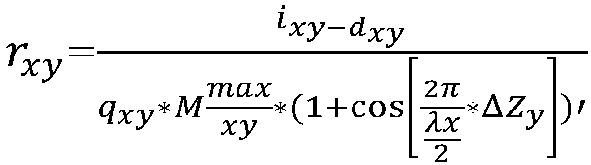 avec ixy = valeur de mesure à la longueur d'onde x sur un pixel y d'un capteur ;dxy = valeur de signal sombre (sans lumière d'excitation) ;qxy = intensité lumineuse irradiée de la mesure ;
 ΔZy = Zmirror,z.- Zsample, avec Zmirror,z = écart du diviseur de faisceau (4) par rapport au miroir de référence et Zsample = écart du diviseur de faisceau (4) par rapport à la surface de l'objet.
Applications Claiming Priority (2)
| Application Number | Priority Date | Filing Date | Title |
|---|---|---|---|
| EP19188318.0A EP3770546A1 (fr) | 2019-07-25 | 2019-07-25 | Dispositif et procédé de mesure de profils de hauteur sur un objet |
| PCT/EP2020/070349 WO2021013747A1 (fr) | 2019-07-25 | 2020-07-17 | Dispositif et procédé de mesure de profils surélevés sur un objet |
Publications (3)
| Publication Number | Publication Date |
|---|---|
| EP4004486A1 EP4004486A1 (fr) | 2022-06-01 |
| EP4004486B1 true EP4004486B1 (fr) | 2025-03-05 |
| EP4004486C0 EP4004486C0 (fr) | 2025-03-05 |
Family
ID=67438994
Family Applications (2)
| Application Number | Title | Priority Date | Filing Date |
|---|---|---|---|
| EP19188318.0A Withdrawn EP3770546A1 (fr) | 2019-07-25 | 2019-07-25 | Dispositif et procédé de mesure de profils de hauteur sur un objet |
| EP20740328.8A Active EP4004486B1 (fr) | 2019-07-25 | 2020-07-17 | Dispositif et procédé de mesure de profils de hauteur sur un objet |
Family Applications Before (1)
| Application Number | Title | Priority Date | Filing Date |
|---|---|---|---|
| EP19188318.0A Withdrawn EP3770546A1 (fr) | 2019-07-25 | 2019-07-25 | Dispositif et procédé de mesure de profils de hauteur sur un objet |
Country Status (4)
| Country | Link |
|---|---|
| US (1) | US12025424B2 (fr) |
| EP (2) | EP3770546A1 (fr) |
| CN (1) | CN114144635B (fr) |
| WO (1) | WO2021013747A1 (fr) |
Families Citing this family (7)
| Publication number | Priority date | Publication date | Assignee | Title |
|---|---|---|---|---|
| EP3812697A1 (fr) | 2019-10-25 | 2021-04-28 | sentronics metrology GmbH | Dispositif et procédé de mesure de profil d'objets plans pourvus de matériaux inconnus |
| DE102020130814A1 (de) * | 2020-11-20 | 2022-05-25 | Universität Stuttgart | Einzelbild-Tilted Wave Interferometer |
| KR102606069B1 (ko) * | 2020-12-28 | 2023-11-24 | 세메스 주식회사 | 웨이퍼 검사 방법 |
| JP7442145B2 (ja) * | 2021-02-25 | 2024-03-04 | Ckd株式会社 | 三次元計測装置 |
| CN114324242B (zh) * | 2021-12-10 | 2024-10-29 | 江西超联光电科技有限公司 | 一种用于反射镜光学加工原位检测的装置 |
| TW202422036A (zh) * | 2022-07-29 | 2024-06-01 | 美商應用材料股份有限公司 | 空間基因組成像的時延積分採集 |
| CN115560683A (zh) * | 2022-08-05 | 2023-01-03 | 上海精测半导体技术有限公司 | 一种光声测量系统和测量膜厚的方法 |
Family Cites Families (11)
| Publication number | Priority date | Publication date | Assignee | Title |
|---|---|---|---|---|
| JPH085314A (ja) | 1994-06-20 | 1996-01-12 | Canon Inc | 変位測定方法及び変位測定装置 |
| DE19600491C1 (de) * | 1996-01-09 | 1997-07-17 | Ibm | Interferometrische Meßeinrichtung |
| US7050171B1 (en) * | 2002-11-04 | 2006-05-23 | The United States Of America As Represneted By The Secretary Of The Army | Single-exposure interferometer with no moving parts |
| US7528961B2 (en) * | 2005-04-29 | 2009-05-05 | Zygo Corporation | Compensation of turbulent effects of gas in measurement paths of multi-axis interferometers |
| JP4710078B2 (ja) * | 2006-02-01 | 2011-06-29 | 国立大学法人東京工業大学 | 表面形状の測定方法およびこれを用いた装置 |
| JP2011040547A (ja) * | 2009-08-10 | 2011-02-24 | Canon Inc | 計測装置、露光装置及びデバイスの製造方法 |
| KR102345196B1 (ko) * | 2014-04-07 | 2021-12-29 | 노바 메주어링 인스트루먼츠 엘티디. | 광학 위상 측정 방법 및 시스템 |
| DE102014108886B3 (de) * | 2014-06-25 | 2015-11-26 | Universität Kassel | Vorrichtung und Verfahren zur interferometrischen Abstandsbestimmung |
| CN109387155B (zh) * | 2017-08-10 | 2020-09-22 | 上海微电子装备(集团)股份有限公司 | 形貌检测装置与形貌检测方法 |
| EP3477252A1 (fr) * | 2017-10-25 | 2019-05-01 | Unity Semiconductor GmbH | Dispositif de détection de profil de surface d'une surface d'objet par mesure de distance par interférométrie |
| EP3495766B8 (fr) * | 2017-12-06 | 2023-02-08 | Silicon Austria Labs GmbH | Interféromètre de référence et procédé de détermination d'une modification de longueur d'un trajet optique |
-
2019
- 2019-07-25 EP EP19188318.0A patent/EP3770546A1/fr not_active Withdrawn
-
2020
- 2020-07-17 US US17/630,063 patent/US12025424B2/en active Active
- 2020-07-17 WO PCT/EP2020/070349 patent/WO2021013747A1/fr not_active Ceased
- 2020-07-17 EP EP20740328.8A patent/EP4004486B1/fr active Active
- 2020-07-17 CN CN202080053465.7A patent/CN114144635B/zh active Active
Also Published As
| Publication number | Publication date |
|---|---|
| EP3770546A1 (fr) | 2021-01-27 |
| US20220268569A1 (en) | 2022-08-25 |
| CN114144635B (zh) | 2025-04-25 |
| US12025424B2 (en) | 2024-07-02 |
| CN114144635A (zh) | 2022-03-04 |
| WO2021013747A1 (fr) | 2021-01-28 |
| EP4004486A1 (fr) | 2022-06-01 |
| EP4004486C0 (fr) | 2025-03-05 |
Similar Documents
| Publication | Publication Date | Title |
|---|---|---|
| EP4004486B1 (fr) | Dispositif et procédé de mesure de profils de hauteur sur un objet | |
| DE2851750C2 (fr) | ||
| DE102008029459B4 (de) | Verfahren und Vorrichtung zur berührungslosen Abstandsmessung | |
| EP1152236B1 (fr) | Dispositif de mesure optique avec un ellipsomètre | |
| DE10163027B4 (de) | Objektlageermittlungsverfahren und eine dieses Verfahren verwendende Vorrichtung | |
| DE69423936T2 (de) | Messungen der Krümmung und von Stufenversetzungslinien in Halbleiterprozessen | |
| DE10118760A1 (de) | Verfahren zur Ermittlung der Laufzeitverteilung und Anordnung | |
| EP2194356B1 (fr) | Appareil de mesure optique | |
| DE19807649B4 (de) | Vorrichtung und Verfahren zur dreidimensionalen Messung und Beobachtung dünner Schichten | |
| DE102008033942B3 (de) | Faseroptisches Mehrwellenlängeninterferometer (MWLI) zur absoluten Vermessung von Abständen und Topologien von Oberflächen in großem Arbeitsabstand | |
| EP3477252A1 (fr) | Dispositif de détection de profil de surface d'une surface d'objet par mesure de distance par interférométrie | |
| DE102011085599B3 (de) | Vorrichtung und Verfahren zur interferometrischen Vermessung eines Objekts | |
| WO2019063403A1 (fr) | Procédé et dispositif de mesure sans contact d'une distance à une surface ou d'une distance entre deux surfaces | |
| DE102004052205A1 (de) | Interferometrischer Multispektral-Sensor und interferometrisches Multispektral-Verfahren zur hochdynamischen Objekt-Tiefenabtastung oder Objekt-Profilerfassung | |
| DE19717885A1 (de) | Verfahren und Vorrichtung mit zwei gleichzeitig benutzten Beobachtungskameras, welche dreidimensionale Messungen am Ort und in Echtzeit von einer komplexen Struktur auf einem Stapel dünner Schichten während einer Auftragungs- oder Abtragungsoperation gestatten | |
| EP2276999B1 (fr) | Agencement optique d'éclairage d'un objet de mesure et agencement interférométrique pour le mesurage de surfaces d'un objet de mesure | |
| DE102010037207B3 (de) | Rauheits-Messvorrichtung und -Messverfahren | |
| DE102010016462B4 (de) | Schichtmessverfahren und Messvorrichtung | |
| WO2021078609A1 (fr) | Dispositif et procédé pour la mesure du profil d'objets plats comprenant des matériaux inconnus | |
| DE10317826B4 (de) | Verfahren und Vorrichtung zur interferometrischen Messung | |
| DE4404154A1 (de) | Verfahren und Vorrichtung zum optischen Untersuchen einer Oberfläche | |
| DE102015112769A1 (de) | Vorrichtung und Verfahren zur optischen Probenuntersuchung | |
| EP1794572B1 (fr) | Procede d'exploitation d'un systeme interferometrique avec un element de reference pourvu d'une ou plusieurs zones reflechissantes | |
| DE102004013521B4 (de) | Vorrichtung zum Messen eines Profils und kleinster Verschiebungen | |
| WO2026017321A1 (fr) | Appareil et procédé de mesure de tranches |
Legal Events
| Date | Code | Title | Description |
|---|---|---|---|
| STAA | Information on the status of an ep patent application or granted ep patent |
Free format text: STATUS: UNKNOWN |
|
| STAA | Information on the status of an ep patent application or granted ep patent |
Free format text: STATUS: THE INTERNATIONAL PUBLICATION HAS BEEN MADE |
|
| PUAI | Public reference made under article 153(3) epc to a published international application that has entered the european phase |
Free format text: ORIGINAL CODE: 0009012 |
|
| STAA | Information on the status of an ep patent application or granted ep patent |
Free format text: STATUS: REQUEST FOR EXAMINATION WAS MADE |
|
| 17P | Request for examination filed |
Effective date: 20220211 |
|
| AK | Designated contracting states |
Kind code of ref document: A1 Designated state(s): AL AT BE BG CH CY CZ DE DK EE ES FI FR GB GR HR HU IE IS IT LI LT LU LV MC MK MT NL NO PL PT RO RS SE SI SK SM TR |
|
| DAV | Request for validation of the european patent (deleted) | ||
| DAX | Request for extension of the european patent (deleted) | ||
| STAA | Information on the status of an ep patent application or granted ep patent |
Free format text: STATUS: EXAMINATION IS IN PROGRESS |
|
| 17Q | First examination report despatched |
Effective date: 20231222 |
|
| REG | Reference to a national code |
Ref country code: DE Ref legal event code: R079 Free format text: PREVIOUS MAIN CLASS: G01B0009020000 Ipc: G01B0009020150 Ref country code: DE Ref legal event code: R079 Ref document number: 502020010543 Country of ref document: DE Free format text: PREVIOUS MAIN CLASS: G01B0009020000 Ipc: G01B0009020150 |
|
| GRAP | Despatch of communication of intention to grant a patent |
Free format text: ORIGINAL CODE: EPIDOSNIGR1 |
|
| STAA | Information on the status of an ep patent application or granted ep patent |
Free format text: STATUS: GRANT OF PATENT IS INTENDED |
|
| RIC1 | Information provided on ipc code assigned before grant |
Ipc: G01B 11/24 20060101ALI20241025BHEP Ipc: G01B 9/02001 20220101ALI20241025BHEP Ipc: G01B 9/02015 20220101AFI20241025BHEP |
|
| INTG | Intention to grant announced |
Effective date: 20241113 |
|
| RIN1 | Information on inventor provided before grant (corrected) |
Inventor name: SROCKA, BERND |
|
| GRAS | Grant fee paid |
Free format text: ORIGINAL CODE: EPIDOSNIGR3 |
|
| GRAA | (expected) grant |
Free format text: ORIGINAL CODE: 0009210 |
|
| STAA | Information on the status of an ep patent application or granted ep patent |
Free format text: STATUS: THE PATENT HAS BEEN GRANTED |
|
| AK | Designated contracting states |
Kind code of ref document: B1 Designated state(s): AL AT BE BG CH CY CZ DE DK EE ES FI FR GB GR HR HU IE IS IT LI LT LU LV MC MK MT NL NO PL PT RO RS SE SI SK SM TR |
|
| REG | Reference to a national code |
Ref country code: GB Ref legal event code: FG4D Free format text: NOT ENGLISH |
|
| REG | Reference to a national code |
Ref country code: CH Ref legal event code: EP |
|
| REG | Reference to a national code |
Ref country code: IE Ref legal event code: FG4D Free format text: LANGUAGE OF EP DOCUMENT: GERMAN |
|
| REG | Reference to a national code |
Ref country code: DE Ref legal event code: R096 Ref document number: 502020010543 Country of ref document: DE |
|
| U01 | Request for unitary effect filed |
Effective date: 20250305 |
|
| U07 | Unitary effect registered |
Designated state(s): AT BE BG DE DK EE FI FR IT LT LU LV MT NL PT RO SE SI Effective date: 20250320 |
|
| PG25 | Lapsed in a contracting state [announced via postgrant information from national office to epo] |
Ref country code: RS Free format text: LAPSE BECAUSE OF FAILURE TO SUBMIT A TRANSLATION OF THE DESCRIPTION OR TO PAY THE FEE WITHIN THE PRESCRIBED TIME-LIMIT Effective date: 20250605 |
|
| PG25 | Lapsed in a contracting state [announced via postgrant information from national office to epo] |
Ref country code: ES Free format text: LAPSE BECAUSE OF FAILURE TO SUBMIT A TRANSLATION OF THE DESCRIPTION OR TO PAY THE FEE WITHIN THE PRESCRIBED TIME-LIMIT Effective date: 20250305 |
|
| PG25 | Lapsed in a contracting state [announced via postgrant information from national office to epo] |
Ref country code: NO Free format text: LAPSE BECAUSE OF FAILURE TO SUBMIT A TRANSLATION OF THE DESCRIPTION OR TO PAY THE FEE WITHIN THE PRESCRIBED TIME-LIMIT Effective date: 20250605 |
|
| PG25 | Lapsed in a contracting state [announced via postgrant information from national office to epo] |
Ref country code: HR Free format text: LAPSE BECAUSE OF FAILURE TO SUBMIT A TRANSLATION OF THE DESCRIPTION OR TO PAY THE FEE WITHIN THE PRESCRIBED TIME-LIMIT Effective date: 20250305 |
|
| PG25 | Lapsed in a contracting state [announced via postgrant information from national office to epo] |
Ref country code: GR Free format text: LAPSE BECAUSE OF FAILURE TO SUBMIT A TRANSLATION OF THE DESCRIPTION OR TO PAY THE FEE WITHIN THE PRESCRIBED TIME-LIMIT Effective date: 20250606 |
|
| U20 | Renewal fee for the european patent with unitary effect paid |
Year of fee payment: 6 Effective date: 20250729 |
|
| PG25 | Lapsed in a contracting state [announced via postgrant information from national office to epo] |
Ref country code: SM Free format text: LAPSE BECAUSE OF FAILURE TO SUBMIT A TRANSLATION OF THE DESCRIPTION OR TO PAY THE FEE WITHIN THE PRESCRIBED TIME-LIMIT Effective date: 20250305 |
|
| PG25 | Lapsed in a contracting state [announced via postgrant information from national office to epo] |
Ref country code: PL Free format text: LAPSE BECAUSE OF FAILURE TO SUBMIT A TRANSLATION OF THE DESCRIPTION OR TO PAY THE FEE WITHIN THE PRESCRIBED TIME-LIMIT Effective date: 20250305 |
|
| PG25 | Lapsed in a contracting state [announced via postgrant information from national office to epo] |
Ref country code: CZ Free format text: LAPSE BECAUSE OF FAILURE TO SUBMIT A TRANSLATION OF THE DESCRIPTION OR TO PAY THE FEE WITHIN THE PRESCRIBED TIME-LIMIT Effective date: 20250305 |
|
| PG25 | Lapsed in a contracting state [announced via postgrant information from national office to epo] |
Ref country code: SK Free format text: LAPSE BECAUSE OF FAILURE TO SUBMIT A TRANSLATION OF THE DESCRIPTION OR TO PAY THE FEE WITHIN THE PRESCRIBED TIME-LIMIT Effective date: 20250305 |
|
| PG25 | Lapsed in a contracting state [announced via postgrant information from national office to epo] |
Ref country code: IS Free format text: LAPSE BECAUSE OF FAILURE TO SUBMIT A TRANSLATION OF THE DESCRIPTION OR TO PAY THE FEE WITHIN THE PRESCRIBED TIME-LIMIT Effective date: 20250705 |
|
| PLBE | No opposition filed within time limit |
Free format text: ORIGINAL CODE: 0009261 |
|
| STAA | Information on the status of an ep patent application or granted ep patent |
Free format text: STATUS: NO OPPOSITION FILED WITHIN TIME LIMIT |
|
| REG | Reference to a national code |
Ref country code: CH Ref legal event code: L10 Free format text: ST27 STATUS EVENT CODE: U-0-0-L10-L00 (AS PROVIDED BY THE NATIONAL OFFICE) Effective date: 20260114 |
|
| 26N | No opposition filed |
Effective date: 20251208 |
|
| REG | Reference to a national code |
Ref country code: CH Ref legal event code: H13 Free format text: ST27 STATUS EVENT CODE: U-0-0-H10-H13 (AS PROVIDED BY THE NATIONAL OFFICE) Effective date: 20260224 |
|
| GBPC | Gb: european patent ceased through non-payment of renewal fee |
Effective date: 20250717 |
|
| PG25 | Lapsed in a contracting state [announced via postgrant information from national office to epo] |
Ref country code: GB Free format text: LAPSE BECAUSE OF NON-PAYMENT OF DUE FEES Effective date: 20250717 |
|
| PG25 | Lapsed in a contracting state [announced via postgrant information from national office to epo] |
Ref country code: CH Free format text: LAPSE BECAUSE OF NON-PAYMENT OF DUE FEES Effective date: 20250731 |