EP4004507B1 - Verfahren zur herstellung eines mikrobolometers mit einem empfindlichen material auf basis von vanadiumoxid - Google Patents
Verfahren zur herstellung eines mikrobolometers mit einem empfindlichen material auf basis von vanadiumoxid Download PDFInfo
- Publication number
- EP4004507B1 EP4004507B1 EP20749831.2A EP20749831A EP4004507B1 EP 4004507 B1 EP4004507 B1 EP 4004507B1 EP 20749831 A EP20749831 A EP 20749831A EP 4004507 B1 EP4004507 B1 EP 4004507B1
- Authority
- EP
- European Patent Office
- Prior art keywords
- sensitive material
- temperature
- equal
- compound
- electrical resistivity
- Prior art date
- Legal status (The legal status is an assumption and is not a legal conclusion. Google has not performed a legal analysis and makes no representation as to the accuracy of the status listed.)
- Active
Links
Images


Classifications
-
- G—PHYSICS
- G01—MEASURING; TESTING
- G01J—MEASUREMENT OF INTENSITY, VELOCITY, SPECTRAL CONTENT, POLARISATION, PHASE OR PULSE CHARACTERISTICS OF INFRARED, VISIBLE OR ULTRAVIOLET LIGHT; COLORIMETRY; RADIATION PYROMETRY
- G01J5/00—Radiation pyrometry, e.g. infrared or optical thermometry
- G01J5/02—Constructional details
- G01J5/04—Casings
- G01J5/041—Mountings in enclosures or in a particular environment
- G01J5/045—Sealings; Vacuum enclosures; Encapsulated packages; Wafer bonding structures; Getter arrangements
-
- G—PHYSICS
- G01—MEASURING; TESTING
- G01J—MEASUREMENT OF INTENSITY, VELOCITY, SPECTRAL CONTENT, POLARISATION, PHASE OR PULSE CHARACTERISTICS OF INFRARED, VISIBLE OR ULTRAVIOLET LIGHT; COLORIMETRY; RADIATION PYROMETRY
- G01J5/00—Radiation pyrometry, e.g. infrared or optical thermometry
- G01J5/02—Constructional details
- G01J5/04—Casings
- G01J5/046—Materials; Selection of thermal materials
-
- G—PHYSICS
- G01—MEASURING; TESTING
- G01J—MEASUREMENT OF INTENSITY, VELOCITY, SPECTRAL CONTENT, POLARISATION, PHASE OR PULSE CHARACTERISTICS OF INFRARED, VISIBLE OR ULTRAVIOLET LIGHT; COLORIMETRY; RADIATION PYROMETRY
- G01J5/00—Radiation pyrometry, e.g. infrared or optical thermometry
- G01J5/02—Constructional details
- G01J5/08—Optical arrangements
- G01J5/0853—Optical arrangements having infrared absorbers other than the usual absorber layers deposited on infrared detectors like bolometers, wherein the heat propagation between the absorber and the detecting element occurs within a solid
-
- G—PHYSICS
- G01—MEASURING; TESTING
- G01J—MEASUREMENT OF INTENSITY, VELOCITY, SPECTRAL CONTENT, POLARISATION, PHASE OR PULSE CHARACTERISTICS OF INFRARED, VISIBLE OR ULTRAVIOLET LIGHT; COLORIMETRY; RADIATION PYROMETRY
- G01J5/00—Radiation pyrometry, e.g. infrared or optical thermometry
- G01J5/10—Radiation pyrometry, e.g. infrared or optical thermometry using electric radiation detectors
- G01J5/20—Radiation pyrometry, e.g. infrared or optical thermometry using electric radiation detectors using resistors, thermistors or semiconductors sensitive to radiation, e.g. photoconductive devices
-
- H—ELECTRICITY
- H10—SEMICONDUCTOR DEVICES; ELECTRIC SOLID-STATE DEVICES NOT OTHERWISE PROVIDED FOR
- H10N—ELECTRIC SOLID-STATE DEVICES NOT OTHERWISE PROVIDED FOR
- H10N15/00—Thermoelectric devices without a junction of dissimilar materials; Thermomagnetic devices, e.g. using the Nernst-Ettingshausen effect
- H10N15/10—Thermoelectric devices using thermal change of the dielectric constant, e.g. working above and below the Curie point
- H10N15/15—Thermoelectric active materials
Definitions
- the field of the invention is that of devices for detecting electromagnetic radiation, for example infrared or terahertz, comprising at least one resistive thermal detector comprising a sensitive material based on vanadium oxide.
- the invention applies in particular to the field of infrared imaging and thermography.
- An electromagnetic radiation detection device may comprise an array of resistive thermal detectors, also called microbolometers, each microbolometer comprising an absorbing portion capable of absorbing the electromagnetic radiation to be detected.
- the absorbing portions are usually in the form of membranes suspended above the substrate by anchoring pillars, and are thermally insulated therefrom by holding and thermal insulation arms.
- anchoring pillars and thermal insulation arms also have an electrical function by electrically connecting the suspended membranes to a reading circuit generally arranged in the substrate.
- the absorbing membrane comprises a sensitive material whose electrical resistivity p varies according to the temperature of the material.
- the sensitive material can be a semiconductor material usually chosen from amorphous silicon and a vanadium oxide VO x .
- the document KR101439263B1 discloses an example method of manufacturing a sensitive material for a microbolometer.
- the invention aims to remedy at least in part the drawbacks of the prior art, and more particularly to propose a method of manufacturing at least one microbolometer comprising a sensitive material based on vanadium oxide whose electrical properties are preserved during the manufacturing process, and more precisely whose risks of degradation of the 1/f noise of the sensitive material, following the manufacturing process, are limited or even eliminated.
- the additional chemical element is preferably selected from arsenic, germanium, and silicon, and is preferably arsenic.
- the step of exposing the sensitive material may include a step of depositing a protective layer covering the sensitive material.
- the step of exposing the sensitive material may comprise a step of depositing an encapsulation layer transparent to the electromagnetic radiation to be detected intended to define a cavity in which the microbolometer is located.
- the temperature T r is preferably greater than or equal to 330°C, or even equal to 350°C to within 5°C.
- the duration ⁇ t r is preferably greater than or equal to 90min.
- the sensitive material is preferably made at a temperature lower than the temperature T r .
- the invention also relates to a microbolometer comprising a sensitive material formed from: a first compound based on vanadium oxide (VO x ); and at least one additional chemical element selected from arsenic, germanium, silicon and phosphorus, with the exception of nitrogen.
- the sensitive material is amorphous; has an electrical resistivity at room temperature of between 0.1 ⁇ .cm and 30 ⁇ .cm; has a homogeneous chemical composition; and comprises an amount of the additional chemical element, defined as the ratio of the number of atoms of the additional chemical element to that of vanadium, at least equal to 0.012 in the case of arsenic, at least equal to 0.04 in the case of germanium and silicon, and at least equal to 0.12 in the case of phosphorus.
- the amount of oxygen defined as the ratio of the number of oxygen atoms to that of vanadium, can be between 1.42 and 1.94, plus or minus 0.05.
- the sensitive material can be covered with a protective layer of silicon nitride.
- the invention also relates to a device for detecting electromagnetic radiation, comprising a matrix of microbolometers according to any one of the preceding characteristics, the microbolometers being arranged in at least one hermetic cavity delimited by a transparent encapsulation structure.
- electromagnetic radiation to be detected the encapsulation structure comprising at least one layer made of amorphous silicon.
- the sensing device may include a getter material located in the sealed cavity.
- the information relating to the chemical composition of a compound is expressed by its gross chemical formula, conventionally expressed in relation to one (1) atom of vanadium.
- the x value of the quantity of oxygen is the number of oxygen atoms per 1 atom of vanadium
- the y value of the quantity of arsenic is the number of arsenic atoms per 1 atom of vanadium.
- the value of the quantity of the chemical element is given to the nearest 10%.
- the atomic proportion of each chemical element in the compound VO x As y is 1/(1+x+y) for vanadium, x/(1+x+y) for oxygen, and y/(1+x+y) for arsenic.
- the invention relates in particular to a method for manufacturing at least one resistive thermal detector, also called a microbolometer, comprising a sensitive material based on vanadium oxide VO x .
- the microbolometer can be adapted to detect infrared or terahertz radiation.
- the sensitive material comprises a sufficient non-zero quantity of at least one additional chemical element chosen from arsenic As, germanium Ge, silicon Si and phosphorus P, with the exception of nitrogen (N), making it possible to improve the thermal stability of the sensitive material.
- the term 'base compound' refers to a compound based on VO x not containing the additional chemical element
- the term 'modified compound' refers to the base compound in which the additional chemical element has been added.
- the manufacturing method implements at least one step in which the sensitive material is exposed to a temperature higher than room temperature, and lower than or equal to a temperature T r , for a duration lower than or equal to ⁇ t r , for example at 330°C or 350°C, or even 390°C, for 10 min, 30 min, or even 90 min or more.
- the thermal exposure temperature T r is therefore higher than room temperature.
- This thermal exposure step may correspond to the deposition at approximately 330°C of a protective layer, for example made of a silicon nitride SiN or a silicon oxide SiO, covering the sensitive material in order to protect it from any subsequent contamination by chemical elements that may be present. It may also correspond to the production of an encapsulation layer in amorphous silicon, said layer being intended to define a hermetic cavity in which the microbolometer is located. It may also involve an activation at approximately 330°C of a getter material located in the hermetic cavity, this getter material being intended to react with residual gas that may be present in the cavity to maintain the latter at a sufficient vacuum level.
- a protective layer for example made of a silicon nitride SiN or a silicon oxide SiO
- thermal exposure step at temperature T r for duration ⁇ t r can be implemented, generally speaking, within the framework of technological steps of manufacturing the microbolometer carried out after the production of the sensitive material, or even within the framework of technological steps of manufacturing the detection device after the production of the microbolometer(s), in particular for the integration of additional functionalities at the level of the detection chip.
- FIGS. 1A and 1B are schematic and partial views, respectively in perspective and in section along the plane A-A', of a microbolometer 10 of a device 1 for detecting electromagnetic radiation, the microbolometer 10 comprising a sensitive material 15 based on vanadium oxide VO x .
- the microbolometer 10 comprises an absorbent membrane 11 with sensitive material 15 based on vanadium oxide VO x , suspended above a substrate 2 by anchoring pillars 12 and thermal insulation arms 13, as well as an electronic control and reading circuit (not shown) located in the substrate 2.
- the microbolometer 10 is here adapted to absorb infrared radiation included in the long infrared wavelength band (called LWIR), ranging from 8 ⁇ m to approximately 14 ⁇ m.
- LWIR long infrared wavelength band
- the microbolometer 10 comprises a substrate 2, made in this example from silicon, comprising an electronic circuit (not shown) allowing the control and reading of the microbolometer.
- the electronic circuit comprises portions of lines conductive, for example metallic, separated from each other by a dielectric material, for example a silicon-based mineral material such as a silicon oxide SiO, a silicon nitride SiN, or their alloys. It may comprise for this purpose active electronic elements, for example diodes, transistors, capacitors, resistors, etc., connected by electrical interconnections to the microbolometer 10 on the one hand, and to an interconnection pad (not shown) on the other hand, the latter being intended to electrically connect the detection device 1 to an external electronic device.
- the absorbent membrane 11 may comprise a lower support layer 20 made of an electrically insulating material on which rest two electrodes 21.1, 21.2 distinct from each other, made for example of TiN which exhibits a high absorption of infrared radiation.
- a thin layer of the sensitive material 15 rests on the support layer 20 and comes into contact with each of the two electrodes 21.1, 21.2.
- the sensitive material 15 is here covered with a protective layer 22, made for example of a silicon nitride SiN or a silicon oxide SiO, which makes it possible to prevent any subsequent contamination of the sensitive material 15.
- a protective layer 22 made for example of a silicon nitride SiN or a silicon oxide SiO, which makes it possible to prevent any subsequent contamination of the sensitive material 15.
- the microbolometer 10 may be located in a hermetic cavity defined by an encapsulation structure (not shown), as described in particular in the publication of Dumont et al. entitled Current progress on pixel level packaging for uncooled IRFPA, SPIE Proceedings Vol.8353 (2012 ).
- the encapsulation structure may be formed from a stack of different thin layers, such as an encapsulation layer, for example made of amorphous silicon deposited by CVD or iPVD, covered with a sealing and antireflection layer, for example made of different sub-layers of germanium and zinc sulfide, deposited for example by EBPVD, IBS or other.
- an encapsulation structure is notably described in the patent application EP3067675 .
- the sensitive material 15 is based on vanadium oxide VO x , that is to say that it is formed from a 'base compound' made from a vanadium oxide VO x in which an additional chemical element chosen from arsenic, germanium, silicon, and phosphorus has been added with the exception of nitrogen.
- the sensitive material 15 therefore does not contain nitrogen: the quantity of nitrogen in the sensitive material 15 is therefore zero or almost zero, that is to say is less than or equal to 0.1% in atomic proportion.
- An additional chemical element is a chemical element added voluntarily to the base compound which is vanadium oxide.
- the sensitive material 15 is amorphous, that is to say that it contains substantially no crystalline phases.
- the base compound has an electrical resistivity of between 1 ⁇ .cm and 30 ⁇ .cm, which corresponds for example to an amount of oxygen x, defined as the ratio between the number of oxygen atoms to the number of vanadium atoms, of between 1.42 and 1.94 to within 0.05.
- the base compound has an electrical resistivity of between 1 ⁇ .cm and 30 ⁇ .cm.
- the modified compound corresponding to the base compound to which the additional chemical element has been added, has an electrical resistivity of between 0.1 ⁇ .cm and 30 ⁇ .cm.
- the amount x of oxygen is identical in the base compound and the modified compound.
- it has a homogeneous chemical composition, that is to say that its chemical composition as defined in an elementary volume of the order of 3nm in diameter is invariant on a large scale (in at least 90%, 95%, or even 99% of its volume).
- the base compound is amorphous and is made from VO x with x between 1.42 and 1.94, plus or minus 0.05, and preferably between 1.56 and 1.94, plus or minus 0.05. It does not have a stoichiometric form. It is thus distinguished from stoichiometric compounds of the type VO 2 , V 2 O 5 , V 3 O 5 .
- the stoichiometric compound V 3 O 5 is a compound that cannot be obtained under the usual conditions of production of such a basic compound VO x of a microbolometer (temperature usually lower than the maximum thermal budget of the reading circuit located in the substrate 2, i.e. lower than 400°C).
- the sensitive material VO x according to the invention can have a quantity x equal to 1.67 without it corresponding to the stoichiometric form V 3 O 5 .
- the probability is almost zero that such a basic compound, i.e.
- amorphous and having an electrical resistivity of between 1 ⁇ .cm and 30 ⁇ .cm approximately can form after annealing at the temperature T r a single stoichiometric crystalline phase V 2 O 3 .
- an amorphous base compound having an oxygen quantity of approximately 1.5 i.e. to within 0.05, several stoichiometric crystalline phases differing in their oxygen quantity are therefore likely to be formed after annealing at T r , including the crystalline phase V 2 O 3 .
- the oxygen quantity of the amorphous base compound is between 1.56 and 1.94, to within 0.05, a single stoichiometric crystalline phase V 2 O 3 cannot form after annealing at T r .
- the native electrical resistivity is then between approximately 2 ⁇ .cm and 30 ⁇ .cm.
- the sensitive material 15 then corresponds to a modified compound, that is to say that it corresponds to the basic compound which has been modified by the addition of at least one additional chemical element chosen from arsenic As, germanium Ge, silicon Si and phosphorus P. As detailed below, it is preferably chosen from arsenic, germanium and silicon, and is preferably arsenic.
- the amount of additional chemical element namely the number of atoms of arsenic As, germanium Ge, silicon Si or phosphorus P, over that of vanadium, is chosen so as to give the sensitive material, which has been exposed to the temperature T r for the duration ⁇ t r , improved thermal stability, more precisely an electrical resistivity ⁇ a
- the native value ⁇ a of the electrical resistivity is that of the sensitive material before it has been exposed to the temperature T r for ⁇ t r .
- the values of the temperature T r and the duration ⁇ t r are such that the first compound based on VO x (therefore without the additional chemical element) has an electrical resistivity at room temperature less than or equal to 10% of its native value. These are values of temperature and duration of the thermal exposure to which the sensitive material 15 will be likely to be subjected during the subsequent stages of manufacturing the microbolometer.
- the amount of additional chemical element (As, Ge, Si and/or P) is then greater than or equal to a so-called effective value, called effective quantity.
- the effective quantity is the minimum, non-zero quantity of the additional chemical element (As, Ge, Si and/or P) from which the sensitive material, having undergone a step of exposure to the temperature T r for the duration ⁇ t r , has an electrical resistivity ⁇ a
- the room temperature may be equal to 30°C.
- the temperature T r is higher than the room temperature, and is preferably greater than or equal to 330°C, and preferably greater than or equal to 350°C. It may be less than or equal to 400°C.
- the duration ⁇ t r is preferably greater than or equal to a few minutes or tens of minutes, or even a few hours.
- the sensitive material when the sensitive material, whose quantity of the additional chemical element (As, Ge, Si and/or P) is greater than or equal to the effective quantity, has not been exposed to the temperature T r for the duration ⁇ t r , its electrical resistivity at room temperature has the native value ⁇ a .
- the sensitive material After thermal exposure to T r for ⁇ t r , the sensitive material then has an electrical resistivity ⁇ a
- the effective amount depends in particular on the base compound considered, as well as on the chosen values of the temperature T r and the duration ⁇ t r of the thermal exposure.
- a person skilled in the art is able to determine the effective amount, i.e. the minimum amount of the additional chemical element (As, Ge, Si and/or P), to be added to the base compound so that the sensitive material has an electrical resistance ⁇ a
- the effective amount may be chosen, where appropriate, so that the value ⁇ a
- a sensitive material made of vanadium oxide therefore without additional chemical elements such as arsenic, germanium, silicon and phosphorus, has an electrical resistivity ⁇ a
- r drops by an order of magnitude, or even by several orders of magnitude, when the sensitive material has been exposed to a temperature of 300°C or 400°C for 10min or 30min under an inert atmosphere.
- an exposure of a VO x -based compound when it is amorphous and has a native electrical resistivity ⁇ a at room temperature between 1 ⁇ .cm and 30 ⁇ .cm, at a temperature T r for a duration ⁇ t r such that its electrical resistivity ⁇ a
- the 1/f noise also called flicker noise or low frequency noise, comes in particular from fluctuations in the mobility and/or density of free carriers.
- an amorphous compound based on a vanadium oxide VO x for which the electrical resistivity is between 1 ⁇ .cm and 30 ⁇ .cm, is not likely to form a single stoichiometric crystalline phase, after annealing at T r , under the usual conditions for producing such a base compound VO x of a microbolometer (temperature below 400°C).
- the base compound has an amount of oxygen x of the order of approximately 1.42 to 1.94. By approximately, it is meant here that the absolute uncertainty is ⁇ 0.05.
- the electrical resistivity of the base compound can be between 2 ⁇ .cm and 30 ⁇ .cm, its amount of oxygen x then being between 1.56 and 1.94, to within 0.05.
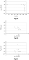
- the Figure 2A illustrates an example of the evolution of the electrical resistivity ⁇ a
- r remains constant and equal to approximately 10 ⁇ .cm up to the temperature T r of approximately 280°C. Then, it shows a sharp decrease, in particular between 300°C and 325°C.
- the electrical resistivity values indicated on the fig.2B for VO x base compounds with annealing correspond to the degraded electrical resistivity following annealing.
- the native values of electrical resistivity are higher and are not shown in the figure.
- the electrical resistivity values for VO x base compounds without annealing (open circles) correspond to the native electrical resistivity of the corresponding compounds.
- the degraded values after annealing are lower but are not shown in the figure.
- the parameter N 1/f representative of the 1/f noise is estimated here from the spectral analysis of a reference electric current flowing in the sensitive material.
- the sensitive material is polarized with a direct current (DC) voltage source adjusted so as to impose the reference current in the sensitive material.
- a very low noise voltage source is used so as not to bias the measurement of the noise of the sensitive material.
- This current is then amplified by a trans-impedance amplifier which delivers a voltage output signal which is the image of the input current.
- the voltage signal is sampled, digitized and digitally processed (Fourier transform) to obtain its spectrum.
- the amplitude of the 1/f noise can be obtained by recording a particular point in the spectrum, for example at 1 Hz or by a least squares calculation method on the low frequency part of the spectrum where the manifestation of the 1/f noise is most marked.
- This increase in the 1/f noise of such a base compound VO x may be the consequence of the beginning of crystallization of the compound, in which distinct crystalline phases appear, which differ from each other by the amount of oxygen, these crystalline phases then being stoichiometric forms.
- the increase in the 1/f noise could thus be linked to the appearance of several stoichiometric crystalline phases, different from each other by the amount of oxygen, and therefore by the loss of the homogeneous character of the chemical composition of the sensitive material, and therefore of its local electrical properties.
- the Figures 3A and 3B illustrate examples of Raman spectra of a basic compound VOx (therefore without added As, Ge, Si or P), initially amorphous, with x equal to approximately 1.85, for different exposures at a temperature T r for a duration ⁇ t r of 90min.
- the Raman spectra of the Figure 3A are centered on a Raman shift range from approximately 100 to 300 cm -1
- those of the Figure 3B are over a Raman shift range from about 700 to 950 cm -1 .
- Curve A o corresponds to the Raman spectrum of a VO 1.85 compound without annealing, and curve A s to that of the support on which the compound in question rests.
- the exposure to high temperature of a basic compound made from VO x and not containing arsenic, germanium, silicon or phosphorus, initially amorphous, and whose native electrical resistivity is between 1 ⁇ .cm and 30 ⁇ .cm leads to at least partial crystallization of the sensitive material, which results in a drop in its electrical resistivity and an increase in the 1/f noise.
- the electrical resistivity at room temperature is a parameter representative of the amorphous or non-amorphous nature of the compound, as well as the 1/f noise.
- the manufacturing process then comprises a step of adding an additional chemical element selected from arsenic, germanium, silicon and phosphorus to the base compound, so as to obtain a modified compound.
- the native electrical resistivity is between 0.1 ⁇ .cm and 30 ⁇ .cm, which corresponds to a non-stoichiometric quantity of oxygen x.
- the quantity of oxygen x in the base compound has not been modified by the addition of the additional chemical element.
- the additional chemical element is arsenic
- the quantity of arsenic to be added to the base compound is determined so that the compound thus modified, when exposed to the temperature T r for the duration ⁇ t r determined beforehand, has an electrical resistivity ⁇ a
- the partial crystallization of the modified compound is limited, causing stoichiometric crystalline phases to appear that differ from each other by the amount of oxygen x, and the degradation of the noise in 1/f is also limited.
- the thermal stability of the properties of the sensitive material is improved when it is subsequently exposed to the temperature T r for the duration ⁇ t r .
- Such a sensitive material is then particularly advantageous in the context of a method for collectively manufacturing a microbolometer array of an electromagnetic radiation detection device.
- the temperature field may exhibit spatial inhomogeneities within a thin-film deposition reactor or an annealing furnace, which may result in a dispersion of the electrical properties of the microbolometers.
- the sensitive material with a sufficient quantity of arsenic, germanium, silicon and/or phosphorus, the microbolometers exhibit better thermal stability during thermal exposure to the temperature T r , thereby reducing the dispersion of the electrical properties of the microbolometers.
- the sensitive material may further comprise a transition metal belonging to period 4 of the periodic table of elements, i.e. scandium Sc, titanium Ti, chromium Cr, manganese Mn, iron Fe, cobalt Co, nickel Ni, copper Cu and/or zinc Zn. It may also comprise other chemical elements, for example yttrium Y, niobium Nb, molybdenum Mo, tantalum Ta, tungsten W, among others.
- FIG. 4A illustrates examples of the evolution of the electrical resistivity ⁇ a
- the samples of the modified compound VO x As y of the sensitive material were made by a technique of deposition of the first compound VO x by ion beam sputtering (IBS), for example by sputtering a vanadium target under an oxidizing atmosphere at a partial pressure of oxygen for example of the order of approximately 10 -4 Torr, followed by implantation of arsenic in the first compound VO x .
- IBS ion beam sputtering
- a vanadium target under an oxidizing atmosphere at a partial pressure of oxygen for example of the order of approximately 10 -4 Torr
- arsenic in the first compound VO x arsenic in the first compound VO x .
- Other techniques for producing the modified compound VO x As y can be used.
- r of the sensitive material is measured at room temperature, here at 30°C, after exposing the sensitive material for 90 min to temperatures of 270°C, 310°C, 330°C, 350°C, 370°C and 390°C.
- Different amounts y of arsenic have been added, namely here 0.004, 0.012, 0.04 and 0.12.
- the amount x of oxygen is equal to 1.9 to within 0.14
- the first compound VO 1.9 has a native resistivity of about 20 ⁇ .cm.
- r presents a drop of a ratio of 10 compared to its native resistivity ⁇ a from a first threshold temperature T th,1 equal to approximately 330°C.
- the additional chemical element it is advantageous for the additional chemical element to be arsenic insofar as it leads to limiting the decrease in the electrical resistivity of the sensitive material with respect to that of the basic compound VO 1.9 .
- the modified compound VO x As 0.12 exhibits a particularly low relative variation in electrical resistivity ⁇ a
- FIG. 4B illustrates examples of the evolution of the electrical resistivity ⁇ a
- the samples of the sensitive material VO x Ge y are obtained in a manner similar to that described previously, i.e. by implantation of germanium in a material VO x obtained previously by IBS sputtering.
- the quantity x of oxygen is here equal to 1.9 to within 0.14, which corresponds to a native electrical resistivity of the first compound VO 1.9 equal to 20 ⁇ .cm.
- r presents a drop of a ratio of 10 compared to its native resistivity ⁇ a from a first threshold temperature T th,1 equal to approximately 330°C.
- y of germanium greater than or equal to 0.04, and preferably greater than or equal to 0.12 gives the sensitive material greater thermal stability, in terms of electrical resistivity and therefore in terms of 1/f noise.
- the modified compound VO x Ge 0.12 exhibits a particularly low relative variation in electrical resistivity ⁇ a
- FIG. 4C illustrates examples of the evolution of the electrical resistivity ⁇ a
- the samples of the sensitive material VO x Si y are obtained in a similar manner to that described previously, i.e. by silicon implantation in a VO x material previously obtained by IBS spraying.
- the quantity x of oxygen is here equal to 1.9 to within 0.14, which corresponds to a native electrical resistivity of the first VO 1.9 compound equal to 20 ⁇ .cm.
- r presents a drop of a ratio of 10 compared to its native resistivity ⁇ a from a first threshold temperature T th,1 equal to approximately 315°C.
- y of silicon greater than or equal to 0.04, and preferably greater than or equal to 0.12, gives the sensitive material greater thermal stability, in terms of electrical resistivity and therefore in terms of 1/f noise.
- the modified compound VO x Si 0.12 exhibits a particularly low relative variation in electrical resistivity ⁇ a
- FIG. 4D illustrates examples of the evolution of the electrical resistivity ⁇ a
- the samples of the sensitive material VO x P y are obtained in a manner similar to that described previously, i.e. by implantation of phosphorus in a material VO x obtained previously by IBS sputtering.
- the quantity x of oxygen is here equal to 1.9 to within 0.14, which corresponds to a native electrical resistivity of the first compound VO 1.9 equal to 20 ⁇ .cm.
- r presents a drop of a ratio of 10 compared to its native resistivity ⁇ a from a first threshold temperature T th,1 equal to approximately 320°C.
- the electrical resistivity shows a drop of a ratio of 10 compared to the corresponding native resistivities ⁇ a from a second threshold temperature T th,2 equal to approximately 360°C. It therefore follows that adding an amount of phosphorus at least equal to 0.12 to the base compound VO x confers at least approximately 40°C of additional thermal stability to the sensitive material, in terms of electrical resistivity and therefore in terms of 1/f noise.
- the additional chemical element is chosen from arsenic, germanium, silicon, and phosphorus. However, it is preferably chosen from arsenic, germanium, and silicon, since these three chemical elements make it possible to increase the thermal stability of the sensitive material to at least 390°C, which is not the case with phosphorus. This is all the more surprising since these four chemical elements are, with boron, part of the chemical elements that form a vitreous network, that is to say that they are part of the chemical elements whose oxide can form on its own (without any other addition) a stable amorphous material.
- the oxides of the network formers are SiO 2 for silicon, P 2 O 5 for phosphorus, GeO 2 for germanium, and As 2 O 3 for arsenic.
- arsenic, germanium and silicon allow to obtain a better thermal stability than phosphorus.
- silicon and phosphorus would be chemical elements just as effective as each other to the extent that they are, like boron, smaller ions than arsenic and germanium.
- phosphorus is less effective than silicon.
- the additional chemical element is preferably chosen from arsenic, germanium, and silicon.
Landscapes
- Physics & Mathematics (AREA)
- General Physics & Mathematics (AREA)
- Spectroscopy & Molecular Physics (AREA)
- Photometry And Measurement Of Optical Pulse Characteristics (AREA)
- Investigating Or Analyzing Materials By The Use Of Electric Means (AREA)
Claims (12)
- Verfahren zum Herstellen mindestens eines Mikrobolometers (10), das ein empfindliches Material (15) umfasst, wobei das Verfahren ein Begrenzen einer Verschlechterung eines mit dem empfindlichen Material (15) verbundenen Rauschens ermöglicht,∘ wobei das empfindliche Material (15) aus Folgendem ausgebildet ist: einer ersten Verbindung auf Basis von Vanadiumoxid (VOx); und mindestens einem zusätzlichen chemischen Element, das zur ersten Verbindung hinzugefügt und aus Arsen (As), Germanium (Ge), Silizium (Si) und Phosphor (P), außer Stickstoff (N), ausgewählt wird,∘ wobei das Verfahren die folgenden Schritte umfasst:• einen Schritt des Herstellens des empfindlichen Materials (15) in einer dünnen Schicht;• einen Schritt des Aussetzens des empfindlichen Materials (15) gegenüber einer Temperatur Tr, die größer als die Umgebungstemperatur ist, während einer Dauer Δtr, der nach dem Schritt des Herstellens des empfindlichen Materials (15) ausgeführt wird,- wobei dieTemperatur Tr und die Dauer Δtr derart sind, dass die erste Verbindung, die amorph ist und einen nativen Wert für den elektrischen Widerstand bei der Umgebungstemperatur in einem Bereich von 1 Ω.m bis 30 Ω.cm aufweist, nachdem sie einem Schritt des Aussetzens gegenüber der Temperatur Tr während der Dauer Δtr durchlaufen hat, einen elektrischen Widerstand bei Umgebungstemperatur aufweist, der kleiner oder gleich 10 % ihres nativen Werts ist;o wobei das Verfahren ferner die folgenden Schritte umfasst:• Bestimmen einer wirksamen Menge ungleich Null des zusätzlichen chemischen Elements (As, Ge, Si, P), die der ersten Verbindung (VOx) hinzugefügt wird, wodurch eine modifizierte Verbindung gebildet wird, ausgehend von der die modifizierte Verbindung, nachdem sie einem Schritt des Aussetzens gegenüber der Temperatur Tr während der Dauer Δtr durchlaufen hat, einen elektrischen Widerstand ρa|r bei Umgebungstemperatur aufweist, der kleiner oder gleich 10 % ihres nativen Werts ρa ist;• wobei beim Schritt des Herstellens des empfindlichen Materials (15) in einer dünnen Schicht diese aus der modifizierten Verbindung ausgebildet wird, die eine Menge des zusätzlichen chemischen Elements (As, Ge, Si, P) aufweist, die größer oder gleich der zuvor bestimmten wirksamen Menge ist, wobei das empfindliche Material (15) amorph ist, einen nativen Wert für den elektrischen Widerstand bei der Umgebungstemperatur in einem Bereich von 0,1 Ω.m bis 30 Ω.cm sowie eine homogene chemische Zusammensetzung aufweist;• so dass das empfindliche Material (15) somit nach dem Schritt des Aussetzens des empfindlichen Materials (15) gegenüber der Temperatur Tr während der Dauer Δtr ein Rauschen aufweist, dessen Verschlechterung begrenzt worden ist.
- Herstellungsverfahren nach Anspruch 1, wobei das zusätzliche chemische Element aus Arsen, Germanium und Silizium ausgewählt ist und vorzugsweise Arsen ist.
- Herstellungsverfahren nach Anspruch 1 oder 2, wobei der Schritt des Aussetzens des empfindlichen Materials (15) einen Schritt des Aufbringens einer Schutzschicht (22) umfasst, die das empfindliche Material bedeckt.
- Herstellungsverfahren nach einem der Ansprüche 1 bis 3, wobei der Schritt des Aussetzens des empfindlichen Materials (15) einen Schritt des Aufbringens einer Einkapselungsschicht umfasst, die für die zu detektierende elektromagnetische Strahlung transparent und dazu bestimmt ist, einen Hohlraum zu definieren, in dem sich das Mikrobolometer befindet.
- Herstellungsverfahren nach einem der Ansprüche 1 bis 4, wobei die Temperatur Tr größer oder gleich 330 °C ist oder sogar bis auf 5 °C genau gleich 350 °C beträgt.
- Herstellungsverfahren nach einem der Ansprüche 1 bis 5, wobei die Dauer Δtr größer oder gleich 90 Minuten ist.
- Herstellungsverfahren nach einem der Ansprüche 1 bis 6, wobei das empfindliche Material (15) bei einer Temperatur hergestellt wird, die kleiner als die Temperatur Tr ist.
- Mikrobolometer (10), das ein empfindliches Material (15) umfasst, das amorph ist und einen elektrischen Widerstand bei der Umgebungstemperatur zwischen 0,1 Ω.m und 30 Ω.cm aufweist und aus Folgendem ausgebildet ist: einer ersten Verbindung auf Basis von Vanadiumoxid (VOx); und mindestens einem zusätzlichen chemischen Element, das aus Arsen, Germanium, Silizium und Phosphor, außer Stickstoff, ausgewählt wird, dadurch gekennzeichnet, dass das empfindliche Material (15):∘ eine homogene chemische Zusammensetzung aufweist, und∘ eine Menge des zusätzlichen chemischen Elements umfasst, die als ein Verhältnis einer Anzahl von Atomen des zusätzlichen chemischen Elements zu der von Vanadium, mindestens 0,012 im Fall von Arsen, mindestens 0,04 im Fall von Germanium und Silizium und mindestens 0,12 im Fall von Phosphor, definiert ist.
- Mikrobolometer (10) nach Anspruch 8, wobei die Sauerstoffmenge, die als Verhältnis einer Anzahl von Atomen von Sauerstoff zu der von Vanadium definiert ist, zwischen 1,42 und 1,94, bis auf plus/minus 0,05 genau, beträgt.
- Mikrobolometer (10) nach Anspruch 8 oder 9, wobei das empfindliche Material (15) von einer Schutzschicht (22) aus Siliziumnitrid bedeckt ist.
- Detektionsvorrichtung (1) für eine elektromagnetische Strahlung, umfassend eine Anordnung von Mikrobolometern nach einem der Ansprüche 8 bis 10, wobei die Mikrobolometer (10) in mindestens einem hermetischen Hohlraum angeordnet sind, der durch eine Einkapselungsstruktur begrenzt ist, die für die zu detektierende elektromagnetische Strahlung transparent ist, wobei die Einkapselungsstruktur eine aus amorphem Silizium hergestellte Schicht umfasst.
- Detektionsvorrichtung (1) nach Anspruch 11, umfassend ein Gettermaterial, das sich im hermetischen Hohlraum befindet.
Applications Claiming Priority (2)
| Application Number | Priority Date | Filing Date | Title |
|---|---|---|---|
| FR1908688A FR3099573B1 (fr) | 2019-07-30 | 2019-07-30 | Procédé de fabrication d’un microbolomètre comportant un matériau sensible à base d’oxyde de vanadium |
| PCT/EP2020/071170 WO2021018856A1 (fr) | 2019-07-30 | 2020-07-27 | Procede de fabrication d'un microbolometre comportant un materiau sensible a base d'oxyde de vanadium |
Publications (2)
| Publication Number | Publication Date |
|---|---|
| EP4004507A1 EP4004507A1 (de) | 2022-06-01 |
| EP4004507B1 true EP4004507B1 (de) | 2024-09-25 |
Family
ID=69104553
Family Applications (1)
| Application Number | Title | Priority Date | Filing Date |
|---|---|---|---|
| EP20749831.2A Active EP4004507B1 (de) | 2019-07-30 | 2020-07-27 | Verfahren zur herstellung eines mikrobolometers mit einem empfindlichen material auf basis von vanadiumoxid |
Country Status (8)
| Country | Link |
|---|---|
| US (1) | US12066332B2 (de) |
| EP (1) | EP4004507B1 (de) |
| KR (1) | KR102864299B1 (de) |
| CN (1) | CN114502932B (de) |
| CA (1) | CA3146045A1 (de) |
| FR (1) | FR3099573B1 (de) |
| TW (1) | TWI864061B (de) |
| WO (1) | WO2021018856A1 (de) |
Families Citing this family (1)
| Publication number | Priority date | Publication date | Assignee | Title |
|---|---|---|---|---|
| TWI809689B (zh) * | 2022-01-27 | 2023-07-21 | 鴻海精密工業股份有限公司 | 微測輻射熱計和其製造方法 |
Family Cites Families (25)
| Publication number | Priority date | Publication date | Assignee | Title |
|---|---|---|---|---|
| JP2976924B2 (ja) * | 1997-05-19 | 1999-11-10 | 日本電気株式会社 | 薄膜感温抵抗材料およびその製造方法 |
| JP2001247958A (ja) * | 2000-03-07 | 2001-09-14 | Nec Corp | ボロメータ材料の作製方法及びボロメータ素子 |
| FR2861172B1 (fr) * | 2003-10-15 | 2006-06-02 | Ulis | Detecteur bolometrique, dispositif de detection infrarouge mettant en oeuvre un tel detecteur bolometrique et procede de fabrication de ce detecteur |
| FR2864065B1 (fr) * | 2003-12-22 | 2006-02-24 | Univ Toulouse | Utilisation de ferrites spinelles comme materiau sensible pour dispositifs bolometriques de detection de l'infrarouge. |
| KR100596196B1 (ko) * | 2004-01-29 | 2006-07-03 | 한국과학기술연구원 | 볼로메타용 산화물 박막 및 이를 이용한 적외선 감지소자 |
| FR2910125B1 (fr) * | 2006-12-14 | 2013-07-05 | Commissariat Energie Atomique | Utilisation d'association de monoxyde de fer et d'oxydes spinelles comme materiau sensible destine a la detection de rayonnements infrarouges |
| US8329002B1 (en) * | 2009-03-10 | 2012-12-11 | 4Wave, Inc. | Thin films and methods and machines for forming the thin films |
| WO2011096012A1 (ja) * | 2010-02-03 | 2011-08-11 | 株式会社日立製作所 | 赤外線センサ |
| JP5964543B2 (ja) * | 2010-06-15 | 2016-08-03 | 日本電気株式会社 | ボロメータ型テラヘルツ波検出器 |
| CN101881667B (zh) * | 2010-06-24 | 2015-09-09 | 电子科技大学 | 一种非制冷微测辐射热计及其制备方法 |
| US8765514B1 (en) * | 2010-11-12 | 2014-07-01 | L-3 Communications Corp. | Transitioned film growth for conductive semiconductor materials |
| FR2977937B1 (fr) * | 2011-07-15 | 2013-08-16 | Centre Nat Rech Scient | Detecteur bolometrique a performances ameliorees |
| EP2581721B1 (de) * | 2011-10-10 | 2019-05-08 | Samsung Electronics Co., Ltd | Infrarotwärmedetektor und Herstellungsverfahren dafür |
| CN105163796B (zh) * | 2013-03-15 | 2018-06-01 | Icu医学有限公司 | 医用连接器 |
| KR101498522B1 (ko) * | 2013-07-17 | 2015-03-04 | 한국광기술원 | 마이크로 볼로미터용 고특성 산화물 박막 제조방법 |
| KR101439263B1 (ko) * | 2013-11-22 | 2014-09-11 | 한국광기술원 | 마이크로 볼로미터용 적외선 감지 박막 제조방법 |
| FR3016211B1 (fr) * | 2014-01-08 | 2018-03-23 | Commissariat A L'energie Atomique Et Aux Energies Alternatives | Materiau sensible pour la detection bolometrique |
| US20150362374A1 (en) * | 2014-06-16 | 2015-12-17 | The Government Of The United States Of America, As Represented By The Secretary Of The Navy | Atomic Layer Deposition of Vanadium Oxide for Microbolometer and Imager |
| FR3023974B1 (fr) * | 2014-07-18 | 2016-07-22 | Ulis | Procede de fabrication d'un dispositif comprenant un boitier hermetique sous vide et un getter |
| FR3033045B1 (fr) | 2015-02-20 | 2020-02-28 | Commissariat A L'energie Atomique Et Aux Energies Alternatives | Dispositif de detection de rayonnement electromagnetique a structure d'encapsulation hermetique a event de liberation |
| US20160273968A1 (en) * | 2015-03-16 | 2016-09-22 | Vlad Joseph Novotny | Sealed Infrared Imagers and Sensors |
| FR3045148B1 (fr) * | 2015-12-15 | 2017-12-08 | Ulis | Dispositif de detection a membranes bolometriques suspendues a fort rendement d'absorption et rapport signal sur bruit |
| CN207964092U (zh) * | 2018-02-06 | 2018-10-12 | 无锡元创华芯微机电有限公司 | 一种高红外吸收的非制冷红外辐射热计 |
| FR3077879B1 (fr) * | 2018-02-15 | 2021-08-27 | Commissariat Energie Atomique | Procede de fabrication d'un microbolometre a materiau sensible a base d'oxyde de vanadium |
| FR3077878B1 (fr) * | 2018-02-15 | 2022-02-04 | Commissariat Energie Atomique | Procede de fabrication d'un microbolometre a materiau sensible a base d'oxyde de vanadium |
-
2019
- 2019-07-30 FR FR1908688A patent/FR3099573B1/fr active Active
-
2020
- 2020-07-27 CN CN202080054567.0A patent/CN114502932B/zh active Active
- 2020-07-27 CA CA3146045A patent/CA3146045A1/fr active Pending
- 2020-07-27 US US17/629,995 patent/US12066332B2/en active Active
- 2020-07-27 WO PCT/EP2020/071170 patent/WO2021018856A1/fr not_active Ceased
- 2020-07-27 KR KR1020227006785A patent/KR102864299B1/ko active Active
- 2020-07-27 EP EP20749831.2A patent/EP4004507B1/de active Active
- 2020-07-29 TW TW109125576A patent/TWI864061B/zh active
Also Published As
| Publication number | Publication date |
|---|---|
| FR3099573A1 (fr) | 2021-02-05 |
| TW202107051A (zh) | 2021-02-16 |
| US20220252456A1 (en) | 2022-08-11 |
| EP4004507A1 (de) | 2022-06-01 |
| KR102864299B1 (ko) | 2025-09-25 |
| CN114502932A (zh) | 2022-05-13 |
| CA3146045A1 (fr) | 2021-02-04 |
| KR20220075310A (ko) | 2022-06-08 |
| FR3099573B1 (fr) | 2021-07-23 |
| TWI864061B (zh) | 2024-12-01 |
| CN114502932B (zh) | 2025-04-29 |
| US12066332B2 (en) | 2024-08-20 |
| WO2021018856A1 (fr) | 2021-02-04 |
Similar Documents
| Publication | Publication Date | Title |
|---|---|---|
| EP3752805B1 (de) | Verfahren zur herstellung eines mikrobolometers mit einem empfindlichen material auf vanadiumoxidbasis | |
| EP3752804B1 (de) | Verfahren zur herstellung eines mikrobolometers mit einem empfindlichen material auf vanadiumoxidbasis | |
| CA2877258A1 (fr) | Materiau sensible pour la detection bolometrique | |
| EP4004507B1 (de) | Verfahren zur herstellung eines mikrobolometers mit einem empfindlichen material auf basis von vanadiumoxid | |
| EP3870945B1 (de) | Verfahren zur herstellung eines mikrobolometers mit thermistormaterial aus vanadiumoxid mit verbesserter leistung | |
| WO2018122382A1 (fr) | Detecteur de rayonnement electromagnetique et notamment de rayonnement infrarouge et procede pour sa realisation | |
| ElGhonimy et al. | Amorphous SiSn alloy: Another candidate material for temperature sensing layers in uncooled microbolometers | |
| FR3066017B1 (fr) | Dispositif pyroelectrique de detection infrarouge comportant un emetteur infrarouge de modulation | |
| FR3156139A1 (fr) | Procede de depot d’une couche a base d’oxyde de vanadium | |
| FR3156195A1 (fr) | Détecteur thermique comportant une membrane absorbante suspendue a isolation thermique améliorée |
Legal Events
| Date | Code | Title | Description |
|---|---|---|---|
| STAA | Information on the status of an ep patent application or granted ep patent |
Free format text: STATUS: UNKNOWN |
|
| STAA | Information on the status of an ep patent application or granted ep patent |
Free format text: STATUS: THE INTERNATIONAL PUBLICATION HAS BEEN MADE |
|
| PUAI | Public reference made under article 153(3) epc to a published international application that has entered the european phase |
Free format text: ORIGINAL CODE: 0009012 |
|
| STAA | Information on the status of an ep patent application or granted ep patent |
Free format text: STATUS: REQUEST FOR EXAMINATION WAS MADE |
|
| 17P | Request for examination filed |
Effective date: 20220126 |
|
| AK | Designated contracting states |
Kind code of ref document: A1 Designated state(s): AL AT BE BG CH CY CZ DE DK EE ES FI FR GB GR HR HU IE IS IT LI LT LU LV MC MK MT NL NO PL PT RO RS SE SI SK SM TR |
|
| DAV | Request for validation of the european patent (deleted) | ||
| DAX | Request for extension of the european patent (deleted) | ||
| GRAP | Despatch of communication of intention to grant a patent |
Free format text: ORIGINAL CODE: EPIDOSNIGR1 |
|
| STAA | Information on the status of an ep patent application or granted ep patent |
Free format text: STATUS: GRANT OF PATENT IS INTENDED |
|
| INTG | Intention to grant announced |
Effective date: 20240515 |
|
| GRAS | Grant fee paid |
Free format text: ORIGINAL CODE: EPIDOSNIGR3 |
|
| GRAA | (expected) grant |
Free format text: ORIGINAL CODE: 0009210 |
|
| STAA | Information on the status of an ep patent application or granted ep patent |
Free format text: STATUS: THE PATENT HAS BEEN GRANTED |
|
| REG | Reference to a national code |
Ref country code: DE Ref legal event code: R081 Ref document number: 602020038321 Country of ref document: DE Owner name: LYNRED, FR Free format text: FORMER OWNER: COMMISSARIAT A L'ENERGIE ATOMIQUE ET AUX ENERGIES ALTERNATIVES, PARIS, FR Ref country code: DE Ref legal event code: R081 Ref document number: 602020038321 Country of ref document: DE Owner name: COMMISSARIAT A L'ENERGIE ATOMIQUE ET AUX ENERG, FR Free format text: FORMER OWNER: COMMISSARIAT A L'ENERGIE ATOMIQUE ET AUX ENERGIES ALTERNATIVES, PARIS, FR |
|
| AK | Designated contracting states |
Kind code of ref document: B1 Designated state(s): AL AT BE BG CH CY CZ DE DK EE ES FI FR GB GR HR HU IE IS IT LI LT LU LV MC MK MT NL NO PL PT RO RS SE SI SK SM TR |
|
| REG | Reference to a national code |
Ref country code: GB Ref legal event code: FG4D Free format text: NOT ENGLISH |
|
| REG | Reference to a national code |
Ref country code: CH Ref legal event code: EP |
|
| REG | Reference to a national code |
Ref country code: DE Ref legal event code: R096 Ref document number: 602020038321 Country of ref document: DE |
|
| REG | Reference to a national code |
Ref country code: IE Ref legal event code: FG4D Free format text: LANGUAGE OF EP DOCUMENT: FRENCH |
|
| RAP4 | Party data changed (patent owner data changed or rights of a patent transferred) |
Owner name: LYNRED Owner name: COMMISSARIAT A L'ENERGIE ATOMIQUE ET AUX ENERGIESALTERNATIVES |
|
| REG | Reference to a national code |
Ref country code: SE Ref legal event code: TRGR |
|
| REG | Reference to a national code |
Ref country code: LT Ref legal event code: MG9D |
|
| PG25 | Lapsed in a contracting state [announced via postgrant information from national office to epo] |
Ref country code: NO Free format text: LAPSE BECAUSE OF FAILURE TO SUBMIT A TRANSLATION OF THE DESCRIPTION OR TO PAY THE FEE WITHIN THE PRESCRIBED TIME-LIMIT Effective date: 20241225 |
|
| PG25 | Lapsed in a contracting state [announced via postgrant information from national office to epo] |
Ref country code: GR Free format text: LAPSE BECAUSE OF FAILURE TO SUBMIT A TRANSLATION OF THE DESCRIPTION OR TO PAY THE FEE WITHIN THE PRESCRIBED TIME-LIMIT Effective date: 20241226 Ref country code: FI Free format text: LAPSE BECAUSE OF FAILURE TO SUBMIT A TRANSLATION OF THE DESCRIPTION OR TO PAY THE FEE WITHIN THE PRESCRIBED TIME-LIMIT Effective date: 20240925 |
|
| PG25 | Lapsed in a contracting state [announced via postgrant information from national office to epo] |
Ref country code: BG Free format text: LAPSE BECAUSE OF FAILURE TO SUBMIT A TRANSLATION OF THE DESCRIPTION OR TO PAY THE FEE WITHIN THE PRESCRIBED TIME-LIMIT Effective date: 20240925 |
|
| PG25 | Lapsed in a contracting state [announced via postgrant information from national office to epo] |
Ref country code: LV Free format text: LAPSE BECAUSE OF FAILURE TO SUBMIT A TRANSLATION OF THE DESCRIPTION OR TO PAY THE FEE WITHIN THE PRESCRIBED TIME-LIMIT Effective date: 20240925 |
|
| PG25 | Lapsed in a contracting state [announced via postgrant information from national office to epo] |
Ref country code: RS Free format text: LAPSE BECAUSE OF FAILURE TO SUBMIT A TRANSLATION OF THE DESCRIPTION OR TO PAY THE FEE WITHIN THE PRESCRIBED TIME-LIMIT Effective date: 20241225 |
|
| REG | Reference to a national code |
Ref country code: NL Ref legal event code: MP Effective date: 20240925 |
|
| PG25 | Lapsed in a contracting state [announced via postgrant information from national office to epo] |
Ref country code: RS Free format text: LAPSE BECAUSE OF FAILURE TO SUBMIT A TRANSLATION OF THE DESCRIPTION OR TO PAY THE FEE WITHIN THE PRESCRIBED TIME-LIMIT Effective date: 20241225 Ref country code: NO Free format text: LAPSE BECAUSE OF FAILURE TO SUBMIT A TRANSLATION OF THE DESCRIPTION OR TO PAY THE FEE WITHIN THE PRESCRIBED TIME-LIMIT Effective date: 20241225 Ref country code: LV Free format text: LAPSE BECAUSE OF FAILURE TO SUBMIT A TRANSLATION OF THE DESCRIPTION OR TO PAY THE FEE WITHIN THE PRESCRIBED TIME-LIMIT Effective date: 20240925 Ref country code: GR Free format text: LAPSE BECAUSE OF FAILURE TO SUBMIT A TRANSLATION OF THE DESCRIPTION OR TO PAY THE FEE WITHIN THE PRESCRIBED TIME-LIMIT Effective date: 20241226 Ref country code: FI Free format text: LAPSE BECAUSE OF FAILURE TO SUBMIT A TRANSLATION OF THE DESCRIPTION OR TO PAY THE FEE WITHIN THE PRESCRIBED TIME-LIMIT Effective date: 20240925 Ref country code: BG Free format text: LAPSE BECAUSE OF FAILURE TO SUBMIT A TRANSLATION OF THE DESCRIPTION OR TO PAY THE FEE WITHIN THE PRESCRIBED TIME-LIMIT Effective date: 20240925 |
|
| REG | Reference to a national code |
Ref country code: AT Ref legal event code: MK05 Ref document number: 1726983 Country of ref document: AT Kind code of ref document: T Effective date: 20240925 |
|
| PG25 | Lapsed in a contracting state [announced via postgrant information from national office to epo] |
Ref country code: NL Free format text: LAPSE BECAUSE OF FAILURE TO SUBMIT A TRANSLATION OF THE DESCRIPTION OR TO PAY THE FEE WITHIN THE PRESCRIBED TIME-LIMIT Effective date: 20240925 |
|
| PG25 | Lapsed in a contracting state [announced via postgrant information from national office to epo] |
Ref country code: IS Free format text: LAPSE BECAUSE OF FAILURE TO SUBMIT A TRANSLATION OF THE DESCRIPTION OR TO PAY THE FEE WITHIN THE PRESCRIBED TIME-LIMIT Effective date: 20250125 Ref country code: PT Free format text: LAPSE BECAUSE OF FAILURE TO SUBMIT A TRANSLATION OF THE DESCRIPTION OR TO PAY THE FEE WITHIN THE PRESCRIBED TIME-LIMIT Effective date: 20250127 |
|
| PG25 | Lapsed in a contracting state [announced via postgrant information from national office to epo] |
Ref country code: RO Free format text: LAPSE BECAUSE OF FAILURE TO SUBMIT A TRANSLATION OF THE DESCRIPTION OR TO PAY THE FEE WITHIN THE PRESCRIBED TIME-LIMIT Effective date: 20240925 Ref country code: SM Free format text: LAPSE BECAUSE OF FAILURE TO SUBMIT A TRANSLATION OF THE DESCRIPTION OR TO PAY THE FEE WITHIN THE PRESCRIBED TIME-LIMIT Effective date: 20240925 |
|
| PG25 | Lapsed in a contracting state [announced via postgrant information from national office to epo] |
Ref country code: ES Free format text: LAPSE BECAUSE OF FAILURE TO SUBMIT A TRANSLATION OF THE DESCRIPTION OR TO PAY THE FEE WITHIN THE PRESCRIBED TIME-LIMIT Effective date: 20240925 |
|
| PG25 | Lapsed in a contracting state [announced via postgrant information from national office to epo] |
Ref country code: EE Free format text: LAPSE BECAUSE OF FAILURE TO SUBMIT A TRANSLATION OF THE DESCRIPTION OR TO PAY THE FEE WITHIN THE PRESCRIBED TIME-LIMIT Effective date: 20240925 Ref country code: AT Free format text: LAPSE BECAUSE OF FAILURE TO SUBMIT A TRANSLATION OF THE DESCRIPTION OR TO PAY THE FEE WITHIN THE PRESCRIBED TIME-LIMIT Effective date: 20240925 |
|
| PG25 | Lapsed in a contracting state [announced via postgrant information from national office to epo] |
Ref country code: PL Free format text: LAPSE BECAUSE OF FAILURE TO SUBMIT A TRANSLATION OF THE DESCRIPTION OR TO PAY THE FEE WITHIN THE PRESCRIBED TIME-LIMIT Effective date: 20240925 Ref country code: CZ Free format text: LAPSE BECAUSE OF FAILURE TO SUBMIT A TRANSLATION OF THE DESCRIPTION OR TO PAY THE FEE WITHIN THE PRESCRIBED TIME-LIMIT Effective date: 20240925 |
|
| PG25 | Lapsed in a contracting state [announced via postgrant information from national office to epo] |
Ref country code: IT Free format text: LAPSE BECAUSE OF FAILURE TO SUBMIT A TRANSLATION OF THE DESCRIPTION OR TO PAY THE FEE WITHIN THE PRESCRIBED TIME-LIMIT Effective date: 20240925 Ref country code: SK Free format text: LAPSE BECAUSE OF FAILURE TO SUBMIT A TRANSLATION OF THE DESCRIPTION OR TO PAY THE FEE WITHIN THE PRESCRIBED TIME-LIMIT Effective date: 20240925 |
|
| REG | Reference to a national code |
Ref country code: DE Ref legal event code: R097 Ref document number: 602020038321 Country of ref document: DE |
|
| PG25 | Lapsed in a contracting state [announced via postgrant information from national office to epo] |
Ref country code: DK Free format text: LAPSE BECAUSE OF FAILURE TO SUBMIT A TRANSLATION OF THE DESCRIPTION OR TO PAY THE FEE WITHIN THE PRESCRIBED TIME-LIMIT Effective date: 20240925 |
|
| PLBE | No opposition filed within time limit |
Free format text: ORIGINAL CODE: 0009261 |
|
| STAA | Information on the status of an ep patent application or granted ep patent |
Free format text: STATUS: NO OPPOSITION FILED WITHIN TIME LIMIT |
|
| 26N | No opposition filed |
Effective date: 20250626 |
|
| PGFP | Annual fee paid to national office [announced via postgrant information from national office to epo] |
Ref country code: DE Payment date: 20250722 Year of fee payment: 6 |
|
| PGFP | Annual fee paid to national office [announced via postgrant information from national office to epo] |
Ref country code: GB Payment date: 20250724 Year of fee payment: 6 |
|
| PGFP | Annual fee paid to national office [announced via postgrant information from national office to epo] |
Ref country code: FR Payment date: 20250722 Year of fee payment: 6 |
|
| PGFP | Annual fee paid to national office [announced via postgrant information from national office to epo] |
Ref country code: SE Payment date: 20250723 Year of fee payment: 6 |
|
| PG25 | Lapsed in a contracting state [announced via postgrant information from national office to epo] |
Ref country code: HR Free format text: LAPSE BECAUSE OF FAILURE TO SUBMIT A TRANSLATION OF THE DESCRIPTION OR TO PAY THE FEE WITHIN THE PRESCRIBED TIME-LIMIT Effective date: 20240925 |
|
| REG | Reference to a national code |
Ref country code: CH Ref legal event code: H13 Free format text: ST27 STATUS EVENT CODE: U-0-0-H10-H13 (AS PROVIDED BY THE NATIONAL OFFICE) Effective date: 20260224 |
|
| PG25 | Lapsed in a contracting state [announced via postgrant information from national office to epo] |
Ref country code: LU Free format text: LAPSE BECAUSE OF NON-PAYMENT OF DUE FEES Effective date: 20250727 |
|
| REG | Reference to a national code |
Ref country code: BE Ref legal event code: MM Effective date: 20250731 |
|
| PG25 | Lapsed in a contracting state [announced via postgrant information from national office to epo] |
Ref country code: BE Free format text: LAPSE BECAUSE OF NON-PAYMENT OF DUE FEES Effective date: 20250731 |
|
| PG25 | Lapsed in a contracting state [announced via postgrant information from national office to epo] |
Ref country code: CH Free format text: LAPSE BECAUSE OF NON-PAYMENT OF DUE FEES Effective date: 20250731 |