EP4004613B1 - Doppelbrechende wellenplatte und verfahren zur herstellung einer welleplatte mit doppelbrechender metaoberfläche - Google Patents
Doppelbrechende wellenplatte und verfahren zur herstellung einer welleplatte mit doppelbrechender metaoberfläche Download PDFInfo
- Publication number
- EP4004613B1 EP4004613B1 EP19938722.6A EP19938722A EP4004613B1 EP 4004613 B1 EP4004613 B1 EP 4004613B1 EP 19938722 A EP19938722 A EP 19938722A EP 4004613 B1 EP4004613 B1 EP 4004613B1
- Authority
- EP
- European Patent Office
- Prior art keywords
- waveplate
- substrate
- angled
- columnar
- birefringent
- Prior art date
- Legal status (The legal status is an assumption and is not a legal conclusion. Google has not performed a legal analysis and makes no representation as to the accuracy of the status listed.)
- Active
Links
Images


Classifications
-
- G—PHYSICS
- G02—OPTICS
- G02B—OPTICAL ELEMENTS, SYSTEMS OR APPARATUS
- G02B1/00—Optical elements characterised by the material of which they are made; Optical coatings for optical elements
- G02B1/002—Optical elements characterised by the material of which they are made; Optical coatings for optical elements made of materials engineered to provide properties not available in nature, e.g. metamaterials
-
- G—PHYSICS
- G02—OPTICS
- G02B—OPTICAL ELEMENTS, SYSTEMS OR APPARATUS
- G02B27/00—Optical systems or apparatus not provided for by any of the groups G02B1/00 - G02B26/00, G02B30/00
- G02B27/28—Optical systems or apparatus not provided for by any of the groups G02B1/00 - G02B26/00, G02B30/00 for polarising
- G02B27/283—Optical systems or apparatus not provided for by any of the groups G02B1/00 - G02B26/00, G02B30/00 for polarising used for beam splitting or combining
-
- G—PHYSICS
- G02—OPTICS
- G02B—OPTICAL ELEMENTS, SYSTEMS OR APPARATUS
- G02B1/00—Optical elements characterised by the material of which they are made; Optical coatings for optical elements
- G02B1/10—Optical coatings produced by application to, or surface treatment of, optical elements
- G02B1/11—Anti-reflection coatings
- G02B1/118—Anti-reflection coatings having sub-optical wavelength surface structures designed to provide an enhanced transmittance, e.g. moth-eye structures
-
- G—PHYSICS
- G02—OPTICS
- G02B—OPTICAL ELEMENTS, SYSTEMS OR APPARATUS
- G02B5/00—Optical elements other than lenses
- G02B5/30—Polarising elements
- G02B5/3083—Birefringent or phase retarding elements
-
- G—PHYSICS
- G02—OPTICS
- G02B—OPTICAL ELEMENTS, SYSTEMS OR APPARATUS
- G02B5/00—Optical elements other than lenses
- G02B5/30—Polarising elements
- G02B5/3083—Birefringent or phase retarding elements
- G02B5/3091—Birefringent or phase retarding elements for use in the UV
-
- G—PHYSICS
- G02—OPTICS
- G02B—OPTICAL ELEMENTS, SYSTEMS OR APPARATUS
- G02B6/00—Light guides; Structural details of arrangements comprising light guides and other optical elements, e.g. couplings
- G02B6/24—Coupling light guides
- G02B6/26—Optical coupling means
- G02B6/27—Optical coupling means with polarisation selective and adjusting means
- G02B6/2706—Optical coupling means with polarisation selective and adjusting means as bulk elements, i.e. free space arrangements external to a light guide, e.g. polarising beam splitters
- G02B6/2713—Optical coupling means with polarisation selective and adjusting means as bulk elements, i.e. free space arrangements external to a light guide, e.g. polarising beam splitters cascade of polarisation selective or adjusting operations
- G02B6/272—Optical coupling means with polarisation selective and adjusting means as bulk elements, i.e. free space arrangements external to a light guide, e.g. polarising beam splitters cascade of polarisation selective or adjusting operations comprising polarisation means for beam splitting and combining
Definitions
- the present disclosure relates to birefringent structures, and more particularly to a system and method for forming a birefringent metasurface in a substrate material.
- Major limiters of laser systems peak power and energy are laser-induced damage processes.
- One of these processes is the formation of filamentation bulk damage.
- the laser system chain for a linearly polarized light beam, however, is simpler.
- amplifiers are designed at the Brewster incidence angle.
- Mirrors and frequency converters are of simpler design as well, usually at one linear polarization. Therefore, the desirable solution is for the light to propagate at a linear polarization through most of the system and to be converted to a circular polarization only at the sections of lowest laser damage threshold, which are usually found at the final optics assembly, and in the ultraviolet (UV) spectrum.
- UV ultraviolet
- the optical component that converts linear to elliptical polarization is a wave retardation plate, which is typically referred to as a "waveplate".
- the waveplate introduces a delay between the two linear polarization components. Specifically, to convert between linear and circular polarizations, the required delay between the two linear polarization components is ⁇ /4 (quarter of a wavelength), and thus the waveplate construction that achieves this conversion is referred to as a quarter wave plate or "QWP".
- D1 ( SU VIN-CENT ET AL: "Advances in optical metasurfaces: fabrication and applications [Invited]", OPTICS EXPRESS, vol. 26, no. 10, 7 May 2018, page 13148, XP 055 867 867 A), D2 ( GRINEVICIUTE LINA ET AL: "Optical anisotropic coatings for polarization control in high-power lasers", SPIE PROCEEDINGS; [PROCEEDINGS OF SPIE ISSN 0277-786X], SPIE, US, vol.
- the present disclosure relates to a waveplate which includes a substrate forming an optic, with the the substrate including an integral portion forming a plurality of angled columnar features on an exposed surface thereof as a result of removal of a portion of a surface of the substrate, leaving the angled columnar features forming a metasurface.
- the plurality of angled columnar features are further ........ aligned parallel with a directional plane formed non-parallel to a reference plane, the reference plane being normal to a surface of the substrate.
- the metasurface forms a birefringent metasurface which forms a portion of the substrate.
- the present disclosure relates to a waveplate for receiving an optical signal.
- the waveplate may comprise a substrate forming an optic, with the substrate including an integral portion forming a metasurface formed on an exposed surface thereof, and extending partially into the substrate.
- the metasurface including a plurality of angled, columnar features formed using a portion of the substrate, the angled columnar features being in a generally uniform grid-like pattern and each having a length of between 1.5 ⁇ -4 ⁇ of a wavelength of the optical signal passing through the waveplate.
- the plurality of angled, columnar features further being aligned parallel with a directional plane defined by an angle ⁇ , where ⁇ is between 40°-75° relative to a reference plane, the reference plane being normal to a surface of the substrate.
- the metasurface forms a birefringent metasurface.
- the present disclosure relates to a method for forming a birefringent waveplate.
- the method comprises providing a substrate, creating a mask on an outer surface of the substrate, and using a material removal process, together with the mask, to remove select material portions from the substrate.
- the material removal process forms a plurality of angled, columnar features which collectively form a birefringent metasurface using a portion of the substrate.
- the birefringent metasurface forms an integral portion of the substrate.
- the present disclosure involves a method and system that enables implementing waveplates to withstand energetic laser beams by directional etching through a nano-particles etch mask at a high incidence angle to obtain a tilted, columnar, birefringent meta-surface formed on the optical substrate.
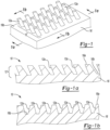
- the waveplate 10 includes a generally uniform pattern of tilted or angled columnar features, which in this embodiment may be termed "columnar projections" 12a.
- the columnar projections 12a collectively form a birefringent metasurface 12 that enables the waveplate 10 to form a subwavelength structure, in this example a quarter wave plate (QWP).
- QWP quarter wave plate
- the methodology described herein may be applied to any form of waveplate, and in fact to any structure or substrate, where one wishes to create a carefully controlled surface pattern on the structure or substrate involving highly controlled material removal with tilted features.
- an etch mask 14 is formed on a surface 16a of a substrate 16.
- the etch mask 14 in one embodiment, may be comprised of subwavelength mask nano-particles 14a deposited on the surface 16a.
- nano-voids 14b may be formed in a material layer (e.g., film) 14' placed, deposited or otherwise formed on the surface 16a.
- material layer e.g., film
- a directional etching method for example, but not limited to, reactive ion etching ("RIE") or reactive ion beam etching (“RIBE”), may then be used to etch the substrate 16 to form the pattern of angled columnar features 12a that collectively form the birefringent metasurface 12.
- RIE reactive ion etching
- RIBE reactive ion beam etching
- the present system and method is agnostic as to how the nano-particle etch mask 14 is applied/formed on the surface 16a of the substrate 16.
- the nano-particle etch mask 14 may also be achieved using thermal annealing (dewetting) of a thin film, or alternatively by other well known methods such as spin/dip coating.
- a suitable etching operation for example RIE or RIBE as mentioned above, may be used to etch the surface 16a to form the pattern of columnar projections 12a that make up the birefringent metasurface 12.
- Figure 3a shows arrows 18 to indicate one example of the angle ⁇ of the trajectory of the reactive ions impinging onto the surface 16a of the substrate 16.
- the angle ⁇ of the columnar projections 12a is an angle that is non-parallel to a reference plane "R", where the reference plane R extends normal to the surface 16a.
- Figure 4 illustrates a plurality of the columnar projections 12a formed in the substrate16 at the angle ⁇ , which collectively form the birefringent metasurface 12.
- the tops of the columnar projections 12a represent what is left of the upper surface 16a, and a new upper surface 16b is formed around a base of each of the columnar projections 12a.
- a depth "L" of each columnar projection 12a will be understood as meaning the overall depth (i.e., or height) of the columnar projection (i.e., the distance that the columnar projection 12a extends down from its upper end (upper surface 16a) to the new upper surface portion 16b (normal to the outer surface 16a), which will be slightly less than the linear length of the columnar projection 12a ("D").
- each of the columnar projections 12a may be about 1 ⁇ m.
- the deposition angle, ⁇ , for the above-mentioned GLAD waveplate was between about 60° and 75°.
- the deposition angle range gives a cos ⁇ value of 0.5-0.25, and therefore, with this estimation, a required etch length (D) of 2-4 ⁇ .
- D required etch length
- this means etched columnar recesses 12a which, in this specific example, will have a length of roughly about 11 ⁇ m.
- angle ⁇ will depend in part of the thickness of the substrate 16, and ⁇ may represent an angle from roughly about 30-60 degrees, and more preferably about 40 degrees to roughly about 50 degrees, and still more preferably an angle approximately between about 60 degrees to 75 degrees. As noted above, these angle values will change depending on the thickness of the substrate 16 that one is working with, and possibly other factors as well.
- Figure 1 illustrates the waveplate 10 after the etch mask 14 has been completely removed, leaving only the substrate 16 with the birefringent metasurface 12, formed by the angled, columnar projections 12a, projecting from the new upper surface 16b of the substrate 16.
- Figures 1a and 1b show the columnar projections 12a from two different views rotated 90 degrees from one another.
- Figure 1c illustrates a birefringent waveplate 10' in accordance with another embodiment of the present disclosure which may be formed using the nano-voids 14b of the nano-voids mask 14' of Figure 2b .
- the columnar features form a pattern of angled, columnar recesses 12a' in the substrate 16', rather than the angled columnar projections 12a.
- Figure 5 is a flowchart 100 illustrating one example of major operations which may be performed in creating the quarter waveplate 10.
- the etch mask 14 is formed on the upper surface of the substrate 16.
- the selected material removal process e.g., RIE, RIBE, etc.
- the selected material removal process may be used to removal selected material portions from the substrate 16 to create the columnar projections 12a which collectively form the birefringent metastructure 12.
- the nano-particles 14a forming the etch mask 14 may then be removed from the outer surface 16a of the substrate 16 to leave the finished quarter waveplate 10. Removal of the nano-particles 14a forming the etch mask 14 will be material dependent, as one example, via a wet process selective etchant.
- a typical etching selectivity aspect ratio between mask metal nano-particles 14a and the etched substrate 16 material is between about 1:5 and 1:50, and could be higher depending on the material system and the process.
- etching selectivity aspect ratio it is meant the ratio of the rate at which the mask and the substrate are being etched away. For example, for a 1:15 etch ratio, a D ⁇ 3 ⁇ channel length requires at least 0.2 ⁇ nano-particle 14a thickness, and about the same nano-particle diameter (or less), which is within the parameter space for mask fabrication methods, such as thin metal film dewetting.
- a few methods to address cases where a larger retardation layer thickness than the resulting retardation layer thickness L is required may be summarized as follows.
- One method is to split the retardation between several independent surfaces. The principal axis of each independent surface should then be aligned, so the retardation layer formed on two or more plates may be easier to manufacture, and then the alignment of the plates may be performed by a suitable calibration procedure.
- a more robust solution at the system level, may be to have the retardation layer formed on two surfaces of the same element. This may be accomplished by splitting a retardation layer into two (e.g, split a QWP into two 1/8 wave plates) although the principal axis would need to be aligned, which creates an additional complexity that would need to be addressed.
- Still another option is using a multi-step etching method. For example, after the mask has eroded by etching, additional deposition of mask will build mainly at the non-etched regions. This is assuming that that the deposition height of the deposited material is substantially smaller than the columnar projection 12a diameter formed between portions of deposited material, so as to not block the deposition of additional material, and since the columnar projections are tilted at an angle relative to the vertical, and the deposition is at normal incidence (or could be further optimized at close to a normal angle opposing the etching direction). After each additional deposition of mask material, further angled etching is enabled.
- a potential mask formation method is forming nano-particles with controlled size by depositing energy to thin metal (i.e., thermal annealing and deweting of thin films).
- Another method may involve nano-particle self-assembly methods (e.g., using block co-polymer construction).
- the present disclosure is agnostic as to how the etch mask 14 is formed, and therefore not limited to any one specific way in which to form the etch mask.
- sub-wavelength structuring of the waveplate 10 affects not only the index difference between the two principal polarizations, but also their refractive index value. Therefore, with proper design, the design of the waveplate 10 layer may also be used to reduce the reflection from the interface.
- the present disclosure thus presents a waveplate 10 and a method for forming the waveplate.
- the method effectively patterns a portion of a layer of a substrate with a metasurface that has a designed birefringence feature.
- the layer is a result of angled directional etching through a nano-particle mask or through a mask having nano-voids, which enables one to create either a pattern of the angled, columnar projections 12a or the angled, columnar recesses 12a'.
- the resulting meta-surface is monolithic with the substrate and a result of the etching process, and has a relatively high laser-induced damage resistivity and structural stability with respect to other previously utilized methods based on material deposition.
- the birefringence of the metasurface layer results from the geometry of the metasurface, and thus applies also to non-birefringent substrates.
- the use of previously proposed methods that spatially control the nano-particle mask characteristics, combined with the present method, is expected to enable spatial control of birefringence of a substrate material.
- the present method allows for simultaneously tailoring the refractive index of the meta-surface layer as well as its birefringence, thus enabling the combination of desired anti-reflective and birefringence properties to the resulting meta-surface layer. These factors are highly important considerations for optics being used with high power lasers.
- angled columnar features 12a and the angled columnar recesses 12a' have been illustrated as being arranged in a uniform, grid-like pattern, it will be appreciated that any arrangement or pattern (uniform or non-uniform) of the columnar projections or columnar recesses may be formed using the teachings of the present disclosure to meet a specific optical application. Accordingly, the present disclosure is not limited to only creating uniform patterns of angled columnar features.
- first, second, third, etc. may be used herein to describe various elements, components, regions, layers and/or sections, these elements, components, regions, layers and/or sections should not be limited by these terms. These terms may be only used to distinguish one element, component, region, layer or section from another region, layer or section. Terms such as “first,” “second,” and other numerical terms when used herein do not imply a sequence or order unless clearly indicated by the context. Thus, a first element, component, region, layer or section discussed below could be termed a second element, component, region, layer or section without departing from the teachings of the example embodiments.
- spatially relative terms such as “inner,” “outer,” “beneath,” “below,” “lower,” “above,” “upper,” and the like, may be used herein for ease of description to describe one element or feature's relationship to another element(s) or feature(s) as illustrated in the figures.
- Spatially relative terms may be intended to encompass different orientations of the device in use or operation in addition to the orientation depicted in the figures. For example, if the device in the figures is turned over, elements described as “below” or “beneath” other elements or features would then be oriented “above” the other elements or features.
- the example term “below” can encompass both an orientation of above and below.
- the device may be otherwise oriented (rotated 90 degrees or at other orientations) and the spatially relative descriptors used herein interpreted accordingly.
Landscapes
- Physics & Mathematics (AREA)
- General Physics & Mathematics (AREA)
- Optics & Photonics (AREA)
- Polarising Elements (AREA)
- Diffracting Gratings Or Hologram Optical Elements (AREA)
Claims (15)
- Wellenplatte (10, 10'), die aufweist:ein Substrat (16, 16'), das eine Optik bildet;wobei das Substrat (16, 16') einen integralen Abschnitt aufweist, der mehrere abgewinkelte, säulenförmige Merkmale (12a) auf einer freiliegenden Oberfläche (16a) davon infolge der Entfernung von einem Teil einer Oberfläche (16a) des Substrats (16, 16') bildet, wobei das Verlassen der abgewinkelten, säulenförmigen Merkmale (12a) eine Metaoberfläche (12) bildet;wobei die mehreren abgewinkelten, säulenförmigen Merkmale (12a) außerdem parallel zu einer Richtungsebene ausgerichtet sind, die nicht parallel zu einer Referenzebene (R) gebildet ist, wobei die Referenzebene (R) senkrecht zu einer Oberfläche (16a) des Substrats (16, 16') ist; undwobei die Metaoberfläche (12) eine doppelbrechende Metaoberfläche (12) bildet, die einen Teil des Substrats (16, 16') bildet.
- Wellenplatte (10, 10') nach Anspruch 1, wobei die Wellenplatte (10, 10') eine Viertelwellenplatte (10, 10') (quarter waveplate (QWP)) aufweist.
- Wellenplatte (10, 10') nach Anspruch 2, wobei:die Metaoberfläche (12) eine Verzögerungsschicht bildet;eine zweiachsige Indexdifferenz durch Δn definiert wird; undeine Dicke "L" der Verzögerungsschicht definiert ist durch: L = λ/4(Δn).
- Wellenplatte (10, 10') nach Anspruch 1, wobei die Wellenplatte (10, 10') aus Quarzglas besteht.
- Wellenplatte (10, 10') nach Anspruch 1, wobei die Vielzahl der abgewinkelten, säulenförmigen Merkmale (12a) jeweils sich in einem Winkel Θ von zwischen 60° und 75° relativ zur Referenzebene (R) erstrecken.
- Wellenplatte (10, 10') nach Anspruch 1, wobei die Vielzahl der abgewinkelten, säulenförmigen Merkmale (12a) jeweils sich in einem Winkel Θ von zwischen etwa 50° und 60° relativ zur Referenzebene (R) erstrecken.
- Wellenplatte (10, 10') nach Anspruch 1, wobei die Vielzahl von abgewinkelten, säulenförmigen Merkmalen (12a) sich jeweils in einem Winkel Θ von etwa 40° relativ zur Referenzebene (R) erstrecken.
- Wellenplatte (10, 10') nach Anspruch 1, wobei die Vielzahl der abgewinkelten, säulenförmigen Merkmale (12a) jeweils eine Länge von mindestens 2λ einer Wellenlänge eines optischen Signals haben, das durch die Wellenplatte (10, 10') läuft.
- Wellenplatte (10, 10') nach Anspruch 8, wobei die Vielzahl der abgewinkelten, säulenförmigen Merkmale (12a) jeweils eine Länge von 2λ - 4λ von einer Wellenlänge eines optischen Signals haben, die durch die Wellenplatte (10, 10') hindurchlaufen.
- Wellenplatte (10, 10') nach Anspruch 1, wobei die Vielzahl der abgewinkelten, säulenförmigen Merkmale (12a) jeweils eine Länge von etwa 1 µm haben.
- Wellenplatte (10, 10') nach Anspruch 1, wobei die Vielzahl von abgewinkelten, säulenförmigen Merkmalen (12a) jeweils eine Länge von etwa 1,5λ einer Wellenlänge eines optischen Signals haben, das durch die Wellenplatte (10, 10') hindurchläuft.
- Wellenplatte (10, 10') nach Anspruch 1, wobei die Vielzahl der abgewinkelten, säulenförmigen Merkmale (12a) eine Vielzahl abgewinkelter, säulenförmiger Vorsprünge (12a) aufweisen, die einen integralen Teil des Substrats (16, 16') bilden.
- Wellenplatte (10, 10') nach Anspruch 1, wobei die Vielzahl der abgewinkelten, säulenförmigen Merkmale (12a) eine Vielzahl abgewinkelter säulenförmiger Aussparungen (12a') aufweisen, die ein integralen Teil des Substrats (16, 16') bilden.
- Verfahren zur Bildung einer doppelbrechenden Wellenplatte (10, 10'), wobei das Verfahren aufweist:Bereitstellen eines Substrats (16, 16');Erzeugen einer Maske (14, 14') auf einer Außenfläche (16a) des Substrats (16, 16'); undVerwenden eines Materialentfernungsprozesses zusammen mit der Maske (14, 14'), um ausgewählte Materialteilbereiche von dem Substrat (16, 16') zu entfernen, um eine Vielzahl abgewinkelter, säulenförmiger Merkmale (12a) zu bilden, die gemeinsam, unter Verwendung eines Teiles des Substrats (16, 16'), eine doppelbrechende Metaoberfläche (12) bilden, wobei die doppelbrechende Metaoberfläche (12) einen integralen Teil des Substrats (16, 16') bildet.
- Verfahren nach Anspruch 14, bei dem das Entfernen ausgewählter Materialteilbereiche des Substrats (16, 16') zur Bildung der abgewinkelten, säulenförmigen Merkmale (12a) das Entfernen ausgewählter Materialteile aufweist, um eine Vielzahl von abgewinkelten, säulenförmigen Vorsprüngen (12a) zu bilden, die integral mit dem Substrat (16, 16') sind.
Applications Claiming Priority (2)
| Application Number | Priority Date | Filing Date | Title |
|---|---|---|---|
| US16/518,500 US11747639B2 (en) | 2019-07-22 | 2019-07-22 | Birefringent waveplate and method for forming a waveplate having a birefringent metasurface |
| PCT/US2019/046527 WO2021015803A1 (en) | 2019-07-22 | 2019-08-14 | Birefringent waveplate and method for forming a waveplate having a birefringent metasurface |
Publications (3)
| Publication Number | Publication Date |
|---|---|
| EP4004613A1 EP4004613A1 (de) | 2022-06-01 |
| EP4004613A4 EP4004613A4 (de) | 2022-10-19 |
| EP4004613B1 true EP4004613B1 (de) | 2025-04-09 |
Family
ID=74191334
Family Applications (1)
| Application Number | Title | Priority Date | Filing Date |
|---|---|---|---|
| EP19938722.6A Active EP4004613B1 (de) | 2019-07-22 | 2019-08-14 | Doppelbrechende wellenplatte und verfahren zur herstellung einer welleplatte mit doppelbrechender metaoberfläche |
Country Status (3)
| Country | Link |
|---|---|
| US (1) | US11747639B2 (de) |
| EP (1) | EP4004613B1 (de) |
| WO (1) | WO2021015803A1 (de) |
Families Citing this family (3)
| Publication number | Priority date | Publication date | Assignee | Title |
|---|---|---|---|---|
| CN114509838B (zh) * | 2022-01-05 | 2023-11-14 | 中国科学院苏州纳米技术与纳米仿生研究所 | 氮化镓基激光器及其内氮化镓纳米超结构的制备方法 |
| US20240369752A1 (en) * | 2023-05-01 | 2024-11-07 | Lawrence Livermore National Security, Llc | Systems and methods for engraving of nano void-dash metasurface into substrate to generate birefringence in the surface layer |
| US20250145518A1 (en) * | 2023-11-07 | 2025-05-08 | Lawrence Livermore National Security, Llc | Low-temperature fabrication method of bulk metamaterial structures for heat-sensitive materials |
Family Cites Families (16)
| Publication number | Priority date | Publication date | Assignee | Title |
|---|---|---|---|---|
| US5116461A (en) * | 1991-04-22 | 1992-05-26 | Motorola, Inc. | Method for fabricating an angled diffraction grating |
| US5212593A (en) * | 1992-02-06 | 1993-05-18 | Svg Lithography Systems, Inc. | Broad band optical reduction system using matched multiple refractive element materials |
| US7164532B2 (en) | 2002-04-19 | 2007-01-16 | Ricoh Company, Ltd. | Diffraction grating, light source unit applying the same therein, and optical head device employing the same |
| JP4386407B2 (ja) * | 2002-11-20 | 2009-12-16 | 富士フイルム株式会社 | 位相差補償システム及び液晶プロジェクタ |
| US7045825B2 (en) | 2004-05-28 | 2006-05-16 | Eastman Kodak Company | Vertical cavity laser producing different color light |
| US20060001969A1 (en) | 2004-07-02 | 2006-01-05 | Nanoopto Corporation | Gratings, related optical devices and systems, and methods of making such gratings |
| JP2013228574A (ja) * | 2012-04-26 | 2013-11-07 | Seiko Epson Corp | 位相差板、及び電子機器 |
| US20170149019A1 (en) * | 2013-03-14 | 2017-05-25 | Q1 Nanosystems Corporation | Three-dimensional optical devices including cavity-containing cores and methods of manufacture |
| US9841606B2 (en) * | 2013-11-04 | 2017-12-12 | Massachusetts Institute Of Technology | Optical filters with engineered birefringence |
| JP6802621B2 (ja) | 2015-06-18 | 2020-12-16 | デクセリアルズ株式会社 | 偏光解消板、それを用いた光学機器及び液晶表示装置、並びに偏光解消板の製造方法 |
| US9632225B2 (en) * | 2015-07-14 | 2017-04-25 | Lumentum Operations Llc | Zoned optical waveplate |
| WO2017053309A1 (en) | 2015-09-23 | 2017-03-30 | Osram Sylvania Inc. | Collimating metalenses and technologies incorporating the same |
| US10612145B2 (en) | 2017-06-16 | 2020-04-07 | Lawrence Livermore National Security, Llc | Nanostructured layer for graded index freeform optics |
| JP2019095554A (ja) * | 2017-11-21 | 2019-06-20 | デクセリアルズ株式会社 | 光学素子及び投射型画像表示装置 |
| US11525945B2 (en) | 2018-06-22 | 2022-12-13 | Lawrence Livermore National Security, Llc | System and method for ablation assisted nanostructure formation for graded index surfaces for optics |
| US10690821B1 (en) * | 2018-12-14 | 2020-06-23 | Applied Materials, Inc. | Methods of producing slanted gratings |
-
2019
- 2019-07-22 US US16/518,500 patent/US11747639B2/en active Active
- 2019-08-14 WO PCT/US2019/046527 patent/WO2021015803A1/en not_active Ceased
- 2019-08-14 EP EP19938722.6A patent/EP4004613B1/de active Active
Also Published As
| Publication number | Publication date |
|---|---|
| WO2021015803A1 (en) | 2021-01-28 |
| US20210026150A1 (en) | 2021-01-28 |
| EP4004613A4 (de) | 2022-10-19 |
| EP4004613A1 (de) | 2022-06-01 |
| US11747639B2 (en) | 2023-09-05 |
Similar Documents
| Publication | Publication Date | Title |
|---|---|---|
| KR101057414B1 (ko) | 광학 소자 및 광학 소자의 제조방법 | |
| Toyota et al. | Fabrication of microcone array for antireflection structured surface using metal dotted pattern | |
| US7727410B2 (en) | Process for formation of three-dimensional photonic crystal | |
| EP4004613B1 (de) | Doppelbrechende wellenplatte und verfahren zur herstellung einer welleplatte mit doppelbrechender metaoberfläche | |
| JP4278597B2 (ja) | 光制御素子 | |
| JP2006512611A (ja) | 光導波路の作製方法 | |
| WO2021008051A1 (zh) | 一种制备高纵宽比二氧化钛的垂直刻蚀工艺 | |
| JP2005157118A (ja) | ブレーズド・ホログラフィック・グレーティング、その製造方法、及びレプリカグレーティング | |
| JP2010169722A (ja) | 光学素子の製造方法及び光学素子 | |
| US20100091369A1 (en) | Double-layer grating | |
| WO2023061987A1 (en) | Anti-reflective structuring of optical elements that include a metasurface | |
| US9013794B2 (en) | Dispersive optical device with three-dimensional photonic crystal | |
| KR20100070681A (ko) | 반사형 편광판의 제조방법 | |
| US20090168170A1 (en) | Wire grid polarizer and method for fabricating the same | |
| US20070076297A1 (en) | Transmission type optical element | |
| JPS6252506A (ja) | グレ−テイング作製方法 | |
| Yavuzcetin et al. | Photonic crystal fabrication in lithium niobate via pattern transfer through wet and dry etched chromium mask | |
| US20030038033A1 (en) | Process for fabricating high aspect ratio embossing tool and microstructures | |
| KR101938990B1 (ko) | 광학 위상 어레이 칩 내 나노 메탈 안테나의 제작 방법 및 그 소자 | |
| US6947223B2 (en) | Multi-focal length miniature refractive element and method for making the same | |
| AU765894B2 (en) | Methods of fabricating etched structures | |
| US12321011B2 (en) | Turning grating device for emission of arbitrary optical beam profiles from waveguides into two-dimensional space | |
| Liu et al. | Optical nanostructures fabricated by SU-8 based nanoimprint lithography | |
| Chen | Metal/multilayer-dielectric coated grating for chirped pulse amplification laser system | |
| US7457501B1 (en) | Electromagnetic energy coupler |
Legal Events
| Date | Code | Title | Description |
|---|---|---|---|
| STAA | Information on the status of an ep patent application or granted ep patent |
Free format text: STATUS: THE INTERNATIONAL PUBLICATION HAS BEEN MADE |
|
| PUAI | Public reference made under article 153(3) epc to a published international application that has entered the european phase |
Free format text: ORIGINAL CODE: 0009012 |
|
| STAA | Information on the status of an ep patent application or granted ep patent |
Free format text: STATUS: REQUEST FOR EXAMINATION WAS MADE |
|
| 17P | Request for examination filed |
Effective date: 20211206 |
|
| AK | Designated contracting states |
Kind code of ref document: A1 Designated state(s): AL AT BE BG CH CY CZ DE DK EE ES FI FR GB GR HR HU IE IS IT LI LT LU LV MC MK MT NL NO PL PT RO RS SE SI SK SM TR |
|
| A4 | Supplementary search report drawn up and despatched |
Effective date: 20220919 |
|
| RIC1 | Information provided on ipc code assigned before grant |
Ipc: G02B 1/118 20150101ALI20220913BHEP Ipc: G02B 1/00 20060101ALI20220913BHEP Ipc: G02B 5/30 20060101AFI20220913BHEP |
|
| DAV | Request for validation of the european patent (deleted) | ||
| DAX | Request for extension of the european patent (deleted) | ||
| P01 | Opt-out of the competence of the unified patent court (upc) registered |
Effective date: 20230526 |
|
| GRAP | Despatch of communication of intention to grant a patent |
Free format text: ORIGINAL CODE: EPIDOSNIGR1 |
|
| STAA | Information on the status of an ep patent application or granted ep patent |
Free format text: STATUS: GRANT OF PATENT IS INTENDED |
|
| INTG | Intention to grant announced |
Effective date: 20241120 |
|
| GRAS | Grant fee paid |
Free format text: ORIGINAL CODE: EPIDOSNIGR3 |
|
| GRAA | (expected) grant |
Free format text: ORIGINAL CODE: 0009210 |
|
| STAA | Information on the status of an ep patent application or granted ep patent |
Free format text: STATUS: THE PATENT HAS BEEN GRANTED |
|
| AK | Designated contracting states |
Kind code of ref document: B1 Designated state(s): AL AT BE BG CH CY CZ DE DK EE ES FI FR GB GR HR HU IE IS IT LI LT LU LV MC MK MT NL NO PL PT RO RS SE SI SK SM TR |
|
| REG | Reference to a national code |
Ref country code: GB Ref legal event code: FG4D |
|
| REG | Reference to a national code |
Ref country code: CH Ref legal event code: EP |
|
| REG | Reference to a national code |
Ref country code: DE Ref legal event code: R096 Ref document number: 602019068588 Country of ref document: DE |
|
| REG | Reference to a national code |
Ref country code: IE Ref legal event code: FG4D |
|
| REG | Reference to a national code |
Ref country code: NL Ref legal event code: MP Effective date: 20250409 |
|
| PG25 | Lapsed in a contracting state [announced via postgrant information from national office to epo] |
Ref country code: NL Free format text: LAPSE BECAUSE OF FAILURE TO SUBMIT A TRANSLATION OF THE DESCRIPTION OR TO PAY THE FEE WITHIN THE PRESCRIBED TIME-LIMIT Effective date: 20250409 |
|
| REG | Reference to a national code |
Ref country code: AT Ref legal event code: MK05 Ref document number: 1784010 Country of ref document: AT Kind code of ref document: T Effective date: 20250409 |
|
| PG25 | Lapsed in a contracting state [announced via postgrant information from national office to epo] |
Ref country code: ES Free format text: LAPSE BECAUSE OF FAILURE TO SUBMIT A TRANSLATION OF THE DESCRIPTION OR TO PAY THE FEE WITHIN THE PRESCRIBED TIME-LIMIT Effective date: 20250409 Ref country code: FI Free format text: LAPSE BECAUSE OF FAILURE TO SUBMIT A TRANSLATION OF THE DESCRIPTION OR TO PAY THE FEE WITHIN THE PRESCRIBED TIME-LIMIT Effective date: 20250409 Ref country code: PT Free format text: LAPSE BECAUSE OF FAILURE TO SUBMIT A TRANSLATION OF THE DESCRIPTION OR TO PAY THE FEE WITHIN THE PRESCRIBED TIME-LIMIT Effective date: 20250811 |
|
| PGFP | Annual fee paid to national office [announced via postgrant information from national office to epo] |
Ref country code: DE Payment date: 20250827 Year of fee payment: 7 |
|
| REG | Reference to a national code |
Ref country code: LT Ref legal event code: MG9D |
|
| PG25 | Lapsed in a contracting state [announced via postgrant information from national office to epo] |
Ref country code: GR Free format text: LAPSE BECAUSE OF FAILURE TO SUBMIT A TRANSLATION OF THE DESCRIPTION OR TO PAY THE FEE WITHIN THE PRESCRIBED TIME-LIMIT Effective date: 20250710 Ref country code: NO Free format text: LAPSE BECAUSE OF FAILURE TO SUBMIT A TRANSLATION OF THE DESCRIPTION OR TO PAY THE FEE WITHIN THE PRESCRIBED TIME-LIMIT Effective date: 20250709 |
|
| PG25 | Lapsed in a contracting state [announced via postgrant information from national office to epo] |
Ref country code: PL Free format text: LAPSE BECAUSE OF FAILURE TO SUBMIT A TRANSLATION OF THE DESCRIPTION OR TO PAY THE FEE WITHIN THE PRESCRIBED TIME-LIMIT Effective date: 20250409 |
|
| PG25 | Lapsed in a contracting state [announced via postgrant information from national office to epo] |
Ref country code: BG Free format text: LAPSE BECAUSE OF FAILURE TO SUBMIT A TRANSLATION OF THE DESCRIPTION OR TO PAY THE FEE WITHIN THE PRESCRIBED TIME-LIMIT Effective date: 20250409 |
|
| PG25 | Lapsed in a contracting state [announced via postgrant information from national office to epo] |
Ref country code: HR Free format text: LAPSE BECAUSE OF FAILURE TO SUBMIT A TRANSLATION OF THE DESCRIPTION OR TO PAY THE FEE WITHIN THE PRESCRIBED TIME-LIMIT Effective date: 20250409 |
|
| PG25 | Lapsed in a contracting state [announced via postgrant information from national office to epo] |
Ref country code: AT Free format text: LAPSE BECAUSE OF FAILURE TO SUBMIT A TRANSLATION OF THE DESCRIPTION OR TO PAY THE FEE WITHIN THE PRESCRIBED TIME-LIMIT Effective date: 20250409 |
|
| PG25 | Lapsed in a contracting state [announced via postgrant information from national office to epo] |
Ref country code: RS Free format text: LAPSE BECAUSE OF FAILURE TO SUBMIT A TRANSLATION OF THE DESCRIPTION OR TO PAY THE FEE WITHIN THE PRESCRIBED TIME-LIMIT Effective date: 20250709 |
|
| PG25 | Lapsed in a contracting state [announced via postgrant information from national office to epo] |
Ref country code: IS Free format text: LAPSE BECAUSE OF FAILURE TO SUBMIT A TRANSLATION OF THE DESCRIPTION OR TO PAY THE FEE WITHIN THE PRESCRIBED TIME-LIMIT Effective date: 20250809 |
|
| PG25 | Lapsed in a contracting state [announced via postgrant information from national office to epo] |
Ref country code: LV Free format text: LAPSE BECAUSE OF FAILURE TO SUBMIT A TRANSLATION OF THE DESCRIPTION OR TO PAY THE FEE WITHIN THE PRESCRIBED TIME-LIMIT Effective date: 20250409 |
|
| REG | Reference to a national code |
Ref country code: DE Ref legal event code: R097 Ref document number: 602019068588 Country of ref document: DE |
|
| PG25 | Lapsed in a contracting state [announced via postgrant information from national office to epo] |
Ref country code: DK Free format text: LAPSE BECAUSE OF FAILURE TO SUBMIT A TRANSLATION OF THE DESCRIPTION OR TO PAY THE FEE WITHIN THE PRESCRIBED TIME-LIMIT Effective date: 20250409 Ref country code: SM Free format text: LAPSE BECAUSE OF FAILURE TO SUBMIT A TRANSLATION OF THE DESCRIPTION OR TO PAY THE FEE WITHIN THE PRESCRIBED TIME-LIMIT Effective date: 20250409 |
|
| PG25 | Lapsed in a contracting state [announced via postgrant information from national office to epo] |
Ref country code: CZ Free format text: LAPSE BECAUSE OF FAILURE TO SUBMIT A TRANSLATION OF THE DESCRIPTION OR TO PAY THE FEE WITHIN THE PRESCRIBED TIME-LIMIT Effective date: 20250409 |
|
| PG25 | Lapsed in a contracting state [announced via postgrant information from national office to epo] |
Ref country code: EE Free format text: LAPSE BECAUSE OF FAILURE TO SUBMIT A TRANSLATION OF THE DESCRIPTION OR TO PAY THE FEE WITHIN THE PRESCRIBED TIME-LIMIT Effective date: 20250409 |
|
| PG25 | Lapsed in a contracting state [announced via postgrant information from national office to epo] |
Ref country code: SK Free format text: LAPSE BECAUSE OF FAILURE TO SUBMIT A TRANSLATION OF THE DESCRIPTION OR TO PAY THE FEE WITHIN THE PRESCRIBED TIME-LIMIT Effective date: 20250409 Ref country code: RO Free format text: LAPSE BECAUSE OF FAILURE TO SUBMIT A TRANSLATION OF THE DESCRIPTION OR TO PAY THE FEE WITHIN THE PRESCRIBED TIME-LIMIT Effective date: 20250409 |
|
| PG25 | Lapsed in a contracting state [announced via postgrant information from national office to epo] |
Ref country code: IT Free format text: LAPSE BECAUSE OF FAILURE TO SUBMIT A TRANSLATION OF THE DESCRIPTION OR TO PAY THE FEE WITHIN THE PRESCRIBED TIME-LIMIT Effective date: 20250409 |
|
| PLBE | No opposition filed within time limit |
Free format text: ORIGINAL CODE: 0009261 |
|
| STAA | Information on the status of an ep patent application or granted ep patent |
Free format text: STATUS: NO OPPOSITION FILED WITHIN TIME LIMIT |
|
| REG | Reference to a national code |
Ref country code: CH Ref legal event code: L10 Free format text: ST27 STATUS EVENT CODE: U-0-0-L10-L00 (AS PROVIDED BY THE NATIONAL OFFICE) Effective date: 20260218 |
|
| 26N | No opposition filed |
Effective date: 20260112 |
|
| REG | Reference to a national code |
Ref country code: CH Ref legal event code: H13 Free format text: ST27 STATUS EVENT CODE: U-0-0-H10-H13 (AS PROVIDED BY THE NATIONAL OFFICE) Effective date: 20260324 |
|
| PG25 | Lapsed in a contracting state [announced via postgrant information from national office to epo] |
Ref country code: MC Free format text: LAPSE BECAUSE OF FAILURE TO SUBMIT A TRANSLATION OF THE DESCRIPTION OR TO PAY THE FEE WITHIN THE PRESCRIBED TIME-LIMIT Effective date: 20250409 |
|
| PG25 | Lapsed in a contracting state [announced via postgrant information from national office to epo] |
Ref country code: LU Free format text: LAPSE BECAUSE OF NON-PAYMENT OF DUE FEES Effective date: 20250814 |
|
| PG25 | Lapsed in a contracting state [announced via postgrant information from national office to epo] |
Ref country code: CH Free format text: LAPSE BECAUSE OF NON-PAYMENT OF DUE FEES Effective date: 20250831 |