EP4004833B1 - Procédé et dispositif d'adressage de qubits et procédé de fabrication du dispositif - Google Patents
Procédé et dispositif d'adressage de qubits et procédé de fabrication du dispositif Download PDFInfo
- Publication number
- EP4004833B1 EP4004833B1 EP20743676.7A EP20743676A EP4004833B1 EP 4004833 B1 EP4004833 B1 EP 4004833B1 EP 20743676 A EP20743676 A EP 20743676A EP 4004833 B1 EP4004833 B1 EP 4004833B1
- Authority
- EP
- European Patent Office
- Prior art keywords
- qubits
- qubit
- electrically conductive
- electromagnetic
- wires
- Prior art date
- Legal status (The legal status is an assumption and is not a legal conclusion. Google has not performed a legal analysis and makes no representation as to the accuracy of the status listed.)
- Active
Links
Images


Classifications
-
- G—PHYSICS
- G06—COMPUTING OR CALCULATING; COUNTING
- G06N—COMPUTING ARRANGEMENTS BASED ON SPECIFIC COMPUTATIONAL MODELS
- G06N10/00—Quantum computing, i.e. information processing based on quantum-mechanical phenomena
- G06N10/40—Physical realisations or architectures of quantum processors or components for manipulating qubits, e.g. qubit coupling or qubit control
-
- H—ELECTRICITY
- H10—SEMICONDUCTOR DEVICES; ELECTRIC SOLID-STATE DEVICES NOT OTHERWISE PROVIDED FOR
- H10N—ELECTRIC SOLID-STATE DEVICES NOT OTHERWISE PROVIDED FOR
- H10N60/00—Superconducting devices
- H10N60/80—Constructional details
- H10N60/82—Current path
-
- G—PHYSICS
- G06—COMPUTING OR CALCULATING; COUNTING
- G06N—COMPUTING ARRANGEMENTS BASED ON SPECIFIC COMPUTATIONAL MODELS
- G06N10/00—Quantum computing, i.e. information processing based on quantum-mechanical phenomena
-
- G—PHYSICS
- G06—COMPUTING OR CALCULATING; COUNTING
- G06N—COMPUTING ARRANGEMENTS BASED ON SPECIFIC COMPUTATIONAL MODELS
- G06N10/00—Quantum computing, i.e. information processing based on quantum-mechanical phenomena
- G06N10/20—Models of quantum computing, e.g. quantum circuits or universal quantum computers
-
- H—ELECTRICITY
- H10—SEMICONDUCTOR DEVICES; ELECTRIC SOLID-STATE DEVICES NOT OTHERWISE PROVIDED FOR
- H10D—INORGANIC ELECTRIC SEMICONDUCTOR DEVICES
- H10D48/00—Individual devices not covered by groups H10D1/00 - H10D44/00
- H10D48/383—Quantum effect devices, e.g. of devices using quantum reflection, diffraction or interference effects
- H10D48/3835—Semiconductor qubit devices comprising a plurality of quantum mechanically interacting semiconductor quantum dots, e.g. Loss-DiVincenzo spin qubits
-
- H—ELECTRICITY
- H10—SEMICONDUCTOR DEVICES; ELECTRIC SOLID-STATE DEVICES NOT OTHERWISE PROVIDED FOR
- H10P—GENERIC PROCESSES OR APPARATUS FOR THE MANUFACTURE OR TREATMENT OF DEVICES COVERED BY CLASS H10
- H10P14/00—Formation of materials, e.g. in the shape of layers or pillars
- H10P14/20—Formation of materials, e.g. in the shape of layers or pillars of semiconductor materials
- H10P14/34—Deposited materials, e.g. layers
- H10P14/3402—Deposited materials, e.g. layers characterised by the chemical composition
- H10P14/3404—Deposited materials, e.g. layers characterised by the chemical composition being Group IVA materials
- H10P14/3406—Carbon, e.g. diamond-like carbon
-
- H—ELECTRICITY
- H10—SEMICONDUCTOR DEVICES; ELECTRIC SOLID-STATE DEVICES NOT OTHERWISE PROVIDED FOR
- H10P—GENERIC PROCESSES OR APPARATUS FOR THE MANUFACTURE OR TREATMENT OF DEVICES COVERED BY CLASS H10
- H10P14/00—Formation of materials, e.g. in the shape of layers or pillars
- H10P14/20—Formation of materials, e.g. in the shape of layers or pillars of semiconductor materials
- H10P14/34—Deposited materials, e.g. layers
- H10P14/3438—Doping during depositing
- H10P14/3441—Conductivity type
- H10P14/3442—N-type
-
- B—PERFORMING OPERATIONS; TRANSPORTING
- B82—NANOTECHNOLOGY
- B82Y—SPECIFIC USES OR APPLICATIONS OF NANOSTRUCTURES; MEASUREMENT OR ANALYSIS OF NANOSTRUCTURES; MANUFACTURE OR TREATMENT OF NANOSTRUCTURES
- B82Y10/00—Nanotechnology for information processing, storage or transmission, e.g. quantum computing or single electron logic
-
- H—ELECTRICITY
- H10—SEMICONDUCTOR DEVICES; ELECTRIC SOLID-STATE DEVICES NOT OTHERWISE PROVIDED FOR
- H10D—INORGANIC ELECTRIC SEMICONDUCTOR DEVICES
- H10D64/00—Electrodes of devices having potential barriers
- H10D64/01—Manufacture or treatment
Definitions
- the present invention relates to a method for addressing qubits according to the preamble of claim 1, a device for addressing qubits according to the preamble of claim 5 and a method for producing the device according to the preamble of claim 13.
- Qubits can not only occupy the states 0 and 1, but can also occupy an intermediate state of 0 and 1 within a certain period of time (coherence time). This state is called superposition.
- qubits can process far more information and therefore offer the potential for computers with unprecedented computing power.
- the production of such qubits, in particular, is currently a topic in science, and a great deal of research is being invested in it.
- scientists are searching for the best way to produce qubits and connect them to form computing units according to quantum laws.
- Qubits can currently be realized using various methods.
- Superconducting qubits are known, which are easy to construct and scalable. Up to 20 qubits have already been entangled in this way. However, they only have extremely short T2 times (transverse relaxation time - spin-spin relaxation) and require cooling to 4°K (-273°C). Therefore, the computers must be installed in specially designed rooms to ensure cooling and the highest possible protection against vibrations, stray electric fields, and residual heat.
- the present invention is based on such solid-state qubits.
- the currently most promising variant of solid-state qubits involves the use of nitrogen vacancy centers (NV centers) in diamonds.
- NV centers nitrogen vacancy centers
- Diamonds offer various mechanical properties, such as their very high hardness, thermal conductivity, and chemical resistance.
- CVD chemical vapor deposition
- Synthetic production offers the advantage of producing diamonds with high isotopic purity and specific crystal defects. This allows diamonds to be equipped with application-specific optical and electronic attributes. These now definable diamond attributes are of great importance for quantum mechanics and have a wide range of applications there.
- Enabling local addressing (shifting the resonant frequency by at least one linewidth) is typically achieved through the use of magnetic fields or different orientations of the qubits. The necessary shift depends on the T2 time. A problem with this approach is that the influence of neighboring qubits, a so-called crossover or crosstalk, cannot be completely avoided when resonance shifting is applied.
- optical addressing As used, for example, in the US 9 317 473 B2 described. Addressing is done optically. To avoid crosstalk between different qubits (registers), they must be arranged at a sufficiently large distance (400 nm to 500 nm). However, direct entanglement of the qubits cannot occur at these distances, so entanglement must be mediated via a so-called dark spin chain of optically non-addressable spins. If, on the other hand, the distance is sufficiently small for direct entanglement to occur, then addressing is done via near-field microscopy (spin resolution). However, indirect entanglement entails functional risks, and the use of near-field microscopy for each individual register is very complex. Furthermore, crosstalk cannot be ruled out in either case. Optical addressing of qubits is also possible from DE 10 2009 033566 A1 known.
- the object of the present invention is therefore to enable the addressing of qubits in a simple manner without the risk of crosstalk. In particular, it should also be possible to easily read the qubits.
- the inventors realized that this task can be solved in a surprising way by addressing a qubit via an electromagnetic field, with the non-addressable qubits being addressed by adapted electromagnetic This allows for very precise and simple addressing of each individual qubit in a set of two or more qubits, even if they are arranged relatively close to each other for the purpose of direct entanglement.
- the inventive method for addressing at least one qubit in a set of two or more qubits is characterized in that the qubit to be addressed is exposed to an electromagnetic field, while at least one other qubit in the set of qubits is exposed to an opposing electromagnetic field such that the electromagnetic field has no effect on the other qubit (for the purpose of pure shielding of this other qubit) or such that the electromagnetic field has a different effect on the other qubit than on the qubit to be addressed (for the purpose of different addressing).
- "addressing" is understood not only to mean the selection of a qubit for changing its state, but also the actual change of its state within the framework of a quantum gate operation (also called quantum gate operations).
- Addressing is thus achieved by selecting the desired qubits and performing quantum gate operations on these qubits. Meanwhile, the other qubits are shielded or the opposing fields are adjusted to optimize their own quantum gate operations.
- Quaternary gate operations are based on changing the spin state of the qubit through the action of a time-varying magnetic field of a specific duration.
- the pulse shape is adjusted to achieve a well-defined state with a low error rate.
- multiple qubits can be addressed simultaneously.
- a carrier frequency in the frequency range of 500 MHz to 50 GHz is used for the pulse shapes for electron spin systems and a frequency range of 1 kHz to 100 MHz for nuclear spin systems.
- the electromagnetic fields and the electromagnetic counterfields are specifically tuned depending on the electromagnetic source and the position of the qubits in relation to this source in order to achieve the desired addressing or non-addressing for the qubits.
- Each qubit can thus be exposed to electromagnetic fields and electromagnetic counterfields at the same time, whereby the superposition of the electromagnetic fields and electromagnetic counterfields simultaneously produces the desired Quantum gate operation and shielding are performed.
- the electromagnetic field itself does not have to serve exactly one quantum gate operation on one qubit, while the opposing electromagnetic field serves exactly to shield the other qubit.
- Mixed forms are possible.
- the electromagnetic field of one qubit and the opposing electromagnetic field of the other qubit can be used to realize the quantum gate operation of the other qubit.
- the electromagnetic field and the opposing electromagnetic field are amplitude-modulated, with a temporal variation between the modulation of the electromagnetic field and the opposing electromagnetic field. This makes the method particularly simple and effective to implement.
- the electromagnetic field and the opposing electromagnetic field are used as electromagnetic near-fields, with the electromagnetic near-fields preferably being magnetic near-fields, which in particular have a frequency in the microwave range and/or kilohertz range. Electromagnetic near-fields couple very well to neighboring qubits, whereby, due to the Laplace equations, a maximum field enhancement occurs near the source of the electromagnetic near-field. These near-fields are independent of the wavelength of the electromagnetic field or opposing field used and can be locally amplified or limited by superposition.
- Fields in the kilohertz range can be used to address the nuclear spins
- fields in the microwave range range 0 GHz to 50 GHz, preferably in the range 2.87 GHz
- fields in the microwave range range 0 GHz to 50 GHz, preferably in the range 2.87 GHz
- NV centers in diamond are used as qubits. These can be produced particularly easily and with high conversion rates, as shown in the DE 10 2019 117 423.6 shown, the relevant content of which is hereby incorporated in its entirety.
- electromagnetic sources preferably electrically conductive structures, are used to provide the electromagnetic fields and counterfields, which are assigned to individual qubits.
- the electromagnetic fields and counterfields can be assigned locally to each individual qubit particularly easily.
- the electrically conductive structures are provided as lines, metallizations, wires, or the like for an electromagnetic field, preferably an electromagnetic high-frequency field.
- the conductive structures should, in particular, be capable of transmitting high frequencies.
- the conductive structures have a smaller dimension (diameter—the length can be greater) than the distance between neighboring qubits. This allows the method to be implemented particularly easily.
- color centers are used as qubits, with the electromagnetic fields and counter-electromagnetic fields being provided by electrically conductive structures that have a smaller dimension than the distance between neighboring qubits. This allows the qubits to be addressed particularly easily.
- the number of conductive structures does not necessarily have to be the same as the number of qubits, because the fields of different conductive structures can be superimposed and gradient fields can also be formed.
- an additional quasi-static electric field could be generated on the conductive structures and addressing could be achieved, for example, via the Stark effect or the Zeeman effect.
- a defined bias is applied to a line (e.g. 10V), and only at the intersection point do the voltages (20V) add up to result in the tuned frequency of the electromagnetic field. This would also make it possible, for example, to perform quantum gate operations on two or three qubits simultaneously. Any errors that may occur due to pulses associated with bias changes could then be corrected using several temporally separated pulse sequences.
- addressing is achieved, for example, by an electric field via the Stark effect or by a semi-static magnetic field via the Zeemann effect.
- the resonant frequency of the qubits is changed, which in turn leads to a selection effect.
- addressing could be achieved by at least three orthogonal or oblique planes of at least X, Y, and Z wires.
- the wires preferably run parallel to a line of qubits.
- the qubits consist of a transparent material, so that a formatting of the qubits, preferably a simultaneous formatting of several, in particular all, qubits, can be carried out by means of optical radiation, preferably laser radiation, as is also described, for example, in the article " Photoelectric imaging and coherent spin-state readout of single nitrogen-vacancy centers in diamond” by P. Siyushev et al., Science, 363, 6428, 728-731 , the relevant content of which is hereby incorporated in its entirety.
- conductive structures are used as electromagnetic sources, they should be as transparent as possible to avoid shadowing the radiation. These could, for example, be lines or wires made of a metal oxide such as ITO (indium zinc oxide). In the case of non-transparent conductive structures, they can be dimensioned so that the radiation can reach the corresponding qubit by diffraction.
- Independent protection is claimed for the device according to the invention for addressing at least one qubit in a set of two or more qubits, which is characterized in that there are means for generating an electromagnetic field which are designed such that the qubit to be addressed can be exposed to the electromagnetic field, and in that there are means for generating at least one opposing electromagnetic field which are designed such that at least one other qubit of the set of qubits can be exposed to the opposing electromagnetic field in such a way that the electromagnetic field of the qubit to be addressed has no effect on the other qubit or that the electromagnetic field has a different effect on the other qubit than on the qubit to be addressed.
- a plurality of first electromagnetic sources preferably first electrically conductive structures, in particular in the form of wires, are arranged in a plane, wherein the qubits have a distance perpendicular to this plane from their respectively assigned electromagnetic source of at most 30 nm, preferably of at most 20 nm, in particular in the range 0 nm to 10 nm.
- These near fields are independent of the wavelength of the electromagnetic field or opposing field used and can be locally amplified or limited by superposition.
- first electromagnetic sources preferably first electrically conductive structures, in particular in the form of wires
- the qubits projected onto this plane have a distance from the respectively assigned first electromagnetic source of at most 20 nm, preferably of at most 10 nm, in particular in the range 0 nm to 5 nm.
- This also makes it particularly easy to generate electromagnetic near fields that couple very strongly to the neighboring qubit, wherein due to the Laplace equations to a maximum field enhancement.
- These near fields are independent of the wavelength of the electromagnetic field or opposing field used and can be locally amplified or limited by superposition.
- At least one second electrically conductive structure is provided as a backside contact of a relatively thin layer, with a layer thickness of at most 100 nm, preferably at most 80 nm, and in particular at most 60 nm being recommended for diamond. This makes readout particularly efficient.
- the electrically conductive structures are arranged one-dimensionally, two-dimensionally or three-dimensionally, wherein preferably two or more levels exist in which electrically conductive wires are arranged, in particular parallel to one another, wherein the electrically conductive structures of different levels are arranged differently, wherein between two levels preferably a electrical insulator.
- the electrically conductive structures of different levels are arranged at an angle to each other, preferably orthogonally to each other, because then electromagnetic fields with elliptical or circular polarization can be generated, which leads to qubits (double quantum transitions, see the article " "Room temperature entanglement between distant single spins in diamond” by F. Dolde et al., Nature Physics, 9, 139-143 (2013 )) can be generated.
- the qubits are color centers, with the means for generating the electromagnetic fields and the counter-electromagnetic fields comprising electrically conductive structures that have a smaller dimension than the distance between neighboring qubits. This allows the qubits to be addressed particularly easily.
- independent protection is claimed for the method according to the invention for producing the device according to the invention, which is characterized in that two or more qubits are generated in a surrounding material and first electrically conductive structures are arranged on the surrounding material.
- the electrically conductive structures such as lines, wires, and metallizations, can be manufactured using various processes. Firstly, printing is possible. Then they can be applied through masks. Furthermore, wires can also be written directly, for example with an AFM tip, as described in the article " Atomic force microscope integrated with a scanning electron microscope for correlative nanofabrication and microscopy" by IW Rangelow et al., J. Vac. Sci. Technol. B 36 (6), Nov/Dec 2018 described.
- the generation of the qubits may comprise the implantation of foreign atoms corresponding to the structure described in the publication " Nanoscale Engineering and Optical Addressing of Single Spins in Diamond", S. Pezzagna et al., small 2010, 6, No. 19, 2117-2121
- the method described is carried out using an AFM tip because this enables very precise positioning of the qubits.
- color centers are created as qubits, and the electrically conductive structures are created such that they have a smaller dimension than the distance between neighboring qubits. This makes the qubits particularly easy to address.
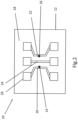
- a first preferred embodiment of the device 10 according to the invention is shown in more detail.
- the device 10 comprises a diamond bulk material 12 in which two qubits 14, 16 are arranged at a depth of approximately 10 nm below the surface 18 of the diamond material 12.
- First electrically conductive wires 20, 22 made of ITO (indium tin oxide) are arranged directly above the two qubits 14, 16. There is also a second electrically conductive wire 24 made of tungsten. For contacting, these wires 20, 22, 24 each have corresponding contact surfaces 26, to which electrical connections (not shown) can be bonded.
- ITO indium tin oxide
- the first two wires 20, 22, which are used for addressing and reading the two qubits 14, 16, are spaced approximately 20 nm to 30 nm apart, which also corresponds to the distance between the two qubits 14, 16. This allows these qubits 14, 16 to become slightly entangled.
- the second wire 24, which forms the ground for reading the qubits 14, 16 is arranged centrally between the two first wires 20, 22 and thus has a distance of 10 nm to 15 nm from these first wires 20, 22. All wires 20, 22, 24 are arranged plane-parallel to one another on the surface 18. In the straight area (cf. Fig. 2 ) between the contact surfaces 26 has a length of 5 nm to 30 nm, preferably 20 nm, and a height and width in the range 1 nm to 10 nm, preferably 5 nm.
- the device 10 now functions in such a way that a simultaneous formatting of the qubits 14, 16 is achieved by a suitable laser pulse through the surface 18, which readily reaches the qubits 14, 16 through the transparent ITO wires 20, 22.
- the laser pulse causes spin polarization, and all qubits 14, 16 transition to the ground state. This results in a defined and known initial state (formatting).
- the wires 20, 22 could also be made of silver or gold, for example, in which case, due to the very narrow dimensions of the wires 20, 22, a diffraction of the LASER pulse around these wires 20, 22 takes place, so that the LASER pulse then also reaches the qubits 14, 16 for formatting.
- the qubits 14, 16 can then be addressed individually or collectively.
- the contacts 26 of the respective wires 20, 22 are subjected to a suitable high-frequency current in the kilohertz range for addressing the nuclear spins of the qubits 14, 16.
- the current flowing in the wires 20, 22 induces a magnetic field that acts on the respective qubit 14, 16.
- Each qubit 14, 16 is thus fed the appropriate magnetic near field, which is used to address it.
- a counter magnetic field is fed to the other qubit 16, 14, which compensates for the magnetic field components of the magnetic near fields used to address qubits 14, 16 at the location of the other qubit 16, 14, so that no crosstalk can occur.
- each qubit 14, 16 could be supplied with suitable LASER pulses separately by suitable illumination means, so that the qubits 14, 16 can be read out individually.
- the device 10 could be manufactured as follows, for example: The qubits 14, 16 are manufactured by doping the diamond 12, followed by first and second tempering steps according to the DE 10 2019 117 423.6 carried out, wherein the steps of contacting with the second wire 24 and masking and contacting with the first wires 20, 22 are suitably integrated into this manufacturing process.
- a diamond 12 is doped with sulfur or another suitable dopant and subjected to a first tempering step at approximately 1000°C. Subsequently, the second tungsten wire 24, together with the respective contact surfaces 26, is vapor-deposited onto the surface 18 of the diamond 12, for example, using a removable mask.
- a contact mask (in Fig. 1 not shown for the sake of clarity) made of glass or silicon carbide is arranged on the surface 18 of the diamond 12 provided with the second wire 24, which has two openings which have the shape of the first wires 20, 22 and which are arranged at the desired distance from the second wire 24.
- Nitrogen is implanted through this mask to create qubits 14 and 16. This also precisely defines the position of qubits 14 and 16 under the first wires 20 and 22 that will be formed later.
- the first wires 20, 22 together with the respective contact surfaces 26 made of ITO are evaporated through the mask, thus completing the device 10.
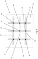
- a second preferred embodiment of the device 50 according to the invention is shown in more detail.
- the device 50 has a diamond layer material 52 in which nine qubits 54, 56, 58, 60, 62, 64, 66, 68, 70 are arranged at a depth of approximately 10 nm below the surface 72 of the diamond material 52.
- first electrically conductive wires 74, 76, 78 made of ITO are arranged in a first plane 80.
- These first wires 74, 76, 78 are covered with an insulator layer 82, which can be formed, for example, from an oxide, in particular SiO2.
- an insulator layer 82 which can be formed, for example, from an oxide, in particular SiO2.
- three further first electrically conductive wires 86, 88, 90 are arranged in a second plane 92.
- the wires 74, 76, 78 in the first plane 80 are aligned plane-parallel to one another, and the wires 86, 88, 90 in the second plane 92 are aligned plane-parallel to one another.
- the wires 74, 76, 78 of the first plane 80 are aligned orthogonally to the wires 86, 88, 90 of the second plane 92, and all wires are electrically insulated from one another. Corresponding contact surfaces have not been shown here to simplify the illustration.
- These first electrically conductive wires 74, 76, 78, 86, 88, 90 also have a height and width in the range of 1 nm to 10 nm, preferably 5 nm.
- the length of the straight sections of the wires 74, 76, 78, 86, 88, 90 each extends approximately 5 nm to 10 nm beyond the outer qubits 54, 56, 58, 60, 64, 66, 68, 70.
- These first electrically conductive wires 74, 76, 78, 86, 88, 90 are in turn used for addressing and reading the qubits 54, 56, 58, 60, 62, 64, 66, 68, 70 and have a spacing of approximately 20 nm to 30 nm in the respective plane 80, 92, which thus also corresponds to the spacing of the wires directly below the virtual intersection points of the wires 74, 76, 78, 86, 88, 90 (cf. Fig. 4 ) arranged qubits 54, 56, 58, 60, 62, 64, 66, 68, 70. Due to the distance of 20 nm to 30 nm, the qubits 54, 56, 58, 60, 62, 64, 66, 68, 70 can easily entangle.
- a common back contact 94 for example made of tungsten, which is located between the diamond layer 52 and a substrate 96.
- This back contact 94 serves as a common ground for the readout of the individual qubits 54, 56, 58, 60, 62, 64, 66, 68, 70.
- the device 50 now functions in such a way that a simultaneous formatting of the qubits 54, 56, 58, 60, 62, 64, 66, 68, 70 by a suitable LASER pulse through the surface 84 which easily reaches the qubits 14, 16 through the transparent ITO wires 74, 76, 78, 86, 88, 90.
- the addressing of the individual qubits 54, 56, 58, 60, 62, 64, 66, 68, 70 can now be achieved by assigning two first wires 74, 76, 78, 86, 88, 90 to each qubit 54, 56, 58, 60, 62, 64, 66, 68, 70, whereby each individual qubit 54, 56, 58, 60, 62, 64, 66, 68, 70 can be individually addressed by the individually formed magnetic near fields by means of different suitable signals on the respectively intersecting first wires 74, 76, 78, 86, 88, 90.
- the qubits 54, 56, 58, 60, 62, 64, 66, 68, 70 are located near crossing points of first wires 74, 76, 78, 86, 88, 90 with respect to a projection onto the planes 80, 92, so that high-frequency magnetic fields applied in the crossing wires 74, 76, 78, 86, 88, 90 overlap, resulting in individual magnetic near fields for each qubit 54, 56, 58, 60, 62, 64, 66, 68, 70.
- the influences of the magnetic near fields of the remaining qubits 54, 56, 58, 60, 62, 64, 66, 68, 70 are eliminated or sufficiently reduced.
- the crossing wires 74, 76, 78, 86, 88, 90 can thus generate elliptically or circularly polarized magnetic near fields for each qubit 54, 56, 58, 60, 62, 64, 66, 68, 70, so that qubit states can be produced.
- a suitable laser pulse is used, for example, whereby the first wires 74, 76, 78, 86, 88, 90 are switched from a current supply to a current measurement, and the back contact serves as ground for the generated photoelectrons.
- each qubit 54, 56, 58, 60, 62, 64, 66, 68, 70 can be assigned its specific measurement signal.
- the device 50 could be manufactured, for example, as follows: The qubits 54, 56, 58, 60, 62, 64, 66, 68, 70 are manufactured by doping the diamond layer material 52, followed by first and second tempering steps according to the DE 10 2019 117 423.6 carried out, whereby the steps of contacting with the rear contact 94 and the contacting with the first wires 74, 76, 78, 86, 88, 90 can be suitably integrated into this manufacturing process.
- a backside contact 94 made of tungsten is deposited on a suitable substrate material 96 by deposition, for example sputtering, and a diamond layer 52 is deposited thereon, for example by vapor deposition.
- This diamond layer 52 is coated with sulfur or another dopant according to the DE 10 2019 117 423.6 doped and subjected to a first tempering step at about 1000°C.
- Nitrogen is then implanted to create qubits 54, 56, 58, 60, 62, 64, 66, 68, 70.
- the nitrogen is implanted with an AFM tip. This procedure is described in principle, for example, in the article " Nanoscale Engineering and Optical Addressing of Single Spins in Diamond", S. Pezzagna et al., small 2010, 6, 19, 2117-2121
- auxiliary markers in the form of graphite markers or metal wires can be arranged outside the surface area to be provided with the qubits 54, 56, 58, 60, 62, 64, 66, 68, 70.
- the first wires 74, 76, 78 of level 80 are drawn on the surface 72 of the diamond material 52 using an AFM tip, and corresponding contact surfaces (not shown) are created.
- a suitable electrical insulator layer 82 such as SiO2 is arranged on the surface 72 of the diamond material 52, thereby covering the first wires 74, 76, 78.
- the first wires 86, 88, 90 of the second level 92 are arranged on the surface 84 of the insulator layer 82, also by drawing with the AFM tip.
- Wire drawing with the AFM tip can be carried out according to the procedure described in the publication "Atomic force microscope integrated with a scanning electron microscope for correlative nanofabrication and microscopy" by IW Rangelow et al., J. Vac. Sci. Technol. B 36 (6), Nov/Dec 2018
- the procedure described in principle can be used. Markers or auxiliary wires can also be used for orientation.
- mask-based methods can also be used to generate the first wires 74, 76, 78, 86, 88, 90, wherein these masks are preferably removed each time in order to ensure the smallest possible distance between the wires 74, 76, 78, 86, 88, 90 and the respectively assigned qubits 54, 56, 58, 60, 62, 64, 66, 68, 70.
- the present invention enables addressing of qubits 14, 16, 54, 56, 58, 60, 62, 64, 66, 68, 70 in a simple manner, without the risk of crosstalk between different qubits 14, 16, 54, 56, 58, 60, 62, 64, 66, 68, 70. Addressing can be carried out both individually and jointly for different qubits 14, 16, 54, 56, 58, 60, 62, 64, 66, 68, 70. In addition, easy readout of qubits 14, 16, 54, 56, 58, 60, 62, 64, 66, 68, 70 is also possible.
Landscapes
- Engineering & Computer Science (AREA)
- General Physics & Mathematics (AREA)
- Theoretical Computer Science (AREA)
- Physics & Mathematics (AREA)
- General Engineering & Computer Science (AREA)
- Mathematical Physics (AREA)
- Evolutionary Computation (AREA)
- Condensed Matter Physics & Semiconductors (AREA)
- Mathematical Analysis (AREA)
- Mathematical Optimization (AREA)
- Pure & Applied Mathematics (AREA)
- Computing Systems (AREA)
- Computational Mathematics (AREA)
- Data Mining & Analysis (AREA)
- Software Systems (AREA)
- Artificial Intelligence (AREA)
- Cathode-Ray Tubes And Fluorescent Screens For Display (AREA)
- Carbon And Carbon Compounds (AREA)
- Semiconductor Memories (AREA)
- Superconductors And Manufacturing Methods Therefor (AREA)
- Devices For Indicating Variable Information By Combining Individual Elements (AREA)
- Optical Modulation, Optical Deflection, Nonlinear Optics, Optical Demodulation, Optical Logic Elements (AREA)
- Measurement And Recording Of Electrical Phenomena And Electrical Characteristics Of The Living Body (AREA)
- Electrodes Of Semiconductors (AREA)
Claims (14)
- Procédé d'adressage d'au moins un qubit (54, 56, 58, 60, 62, 64, 66, 68, 70) issu d'une quantité de deux qubits ou plus (54, 56, 58, 60, 62, 64, 66, 68, 70),
caractérisé en ce que le qubit (54, 56, 58, 60, 62, 64, 66, 68, 70) à adresser est exposé à un champ électromagnétique sous la forme d'un champ proche magnétique pour modifier l'état du qubit (54, 56, 58, 60, 62, 64, 66, 68, 70), tandis qu'au moins un autre qubit de la quantité de qubits (54, 56, 58, 60, 62, 64, 66, 68, 70) est exposé à un contre-champ électromagnétique sous la forme d'un champ proche magnétique de telle sorte que le champ électromagnétique n'exerce aucune action sur l'autre qubit (54, 56, 58, 60, 62, 64, 66, 68, 70) ou que le champ électromagnétique exerce une action sur l'autre qubit (54, 56, 58, 60, 62, 64, 66, 68, 70) autre que sur le qubit (54, 56, 58, 60, 62, 64, 66, 68, 70) à adresser, dans lequel des structures électriquement conductrices (74, 76, 78, 86, 88, 90) sont disposées dans des plans (80, 92) différents, dans lequel les structures (74, 76, 78, 86, 66, 90) électriquement conductrices de différents plans (80, 92) sont disposées de manière oblique les unes par rapport aux autres, dans lequel les qubits (54, 56, 58, 60, 62, 64, 66, 68, 70) se trouvent par rapport à une projection sur les plans (80, 92) à proximité de points d'intersection de premiers fils (74, 76, 78, 86, 88, 90), dans lequel les qubits (54, 56, 58, 60, 62, 64, 66, 68, 70) sont présents en tant que matériau environnant dans une couche en diamant (52), dans lequel le matériau environnant est dopé au soufre, au phosphore ou à l'oxygène, dans lequel des centres NV en diamant (52) sont utilisés en tant que qubits (54, 56, 58, 60, 62, 64, 66, 68, 70). - Procédé selon la revendication 1, caractérisé en ce que les champs proches magnétiques présentent une fréquence dans la plage de micro-ondes et/ou dans la plage de kilohertz et/ou
que des champs proches magnétiques sont générés avec une polarisation elliptique ou circulaire pour générer des qutrits. - Procédé selon la revendication 1 ou 2, caractérisé que les champs électromagnétiques et les contre-champs électromagnétiques sont fournis par des sources électromagnétiques (74, 76, 78, 86, 88, 90), de manière préférée des structures électriquement conductrices, en particulier des câbles, des métallisations ou des fils (74, 76, 78, 86, 88, 90), dans lequel les structures électriquement conductrices (74, 76, 78, 86, 88, 90) possèdent une dimension inférieure à la distance de qubits (54, 56, 58, 60, 62, 64, 66, 68, 70) adjacents.
- Procédé selon l'une quelconque des revendications précédentes, caractérisé en ce que les qubits (54, 56, 58, 60, 62, 64, 66, 68, 70) sont constitués d'un matériau transparent (52), de telle sorte qu'un formatage des qubits (54, 56, 58, 60, 62, 64, 66, 68, 70), de manière préférée un formatage simultané de plusieurs, en particulier de tous les qubits (54, 56, 58, 60, 62, 64, 66, 68, 70) peut être effectué au moyen d'un rayonnement optique, de préférence d'un rayonnement LASER.
- Dispositif d'adressage d'au moins un qubit (54, 56, 58, 60, 62, 64, 66, 68, 70) issu d'une quantité de deux qubits ou plus (54, 56, 58, 60, 62, 64, 66, 68, 70),
caractérisé en ce que le dispositif présente des moyens (74, 76, 78, 86, 88, 90) destinés à générer un champ électromagnétique sous la forme d'un champ proche magnétique, qui sont réalisés de telle sorte que le qubit (54, 56, 58, 60, 62, 64, 66, 68, 70) à adresser peut être exposé au champ électromagnétique pour modifier l'état du qubit (54, 56, 58, 60, 62, 64, 66, 68, 70), et que le dispositif présente des moyens (74, 76, 78, 86, 88, 90) destinés à générer au moins un contre-champ électromagnétique sous la forme d'un champ proche magnétique, qui sont réalisés de telle sorte qu'au moins un autre qubit de la quantité de qubits (54, 56, 58, 60, 62, 64, 66, 68, 70) peut être exposé au contre-champ électromagnétique de telle sorte que le champ électromagnétique n'exerce aucune action sur l'autre qubit (54, 56, 58, 60, 62, 64, 66, 68, 70) ou que le champ électromagnétique exerce une action sur l'autre qubit (54, 56, 58, 60, 62, 64, 66, 68, 70) autre que sur le qubit à adresser (54, 56, 58, 60, 62, 64, 66, 68, 70), dans lequel des structures électriquement conductrices (74, 76, 78, 86, 88, 90) sont disposées dans des plans (80, 92) différents, dans lequel les structures électriquement conductrices (74, 76, 78, 86, 88, 90) de différents plans (80, 92) sont disposées de manière oblique les unes par rapport aux autres, dans lequel les qubits (54, 56, 58, 60, 62, 64, 66, 68, 70) se trouvent par rapport à une projection sur les plans (80, 92) à proximité de points d'intersection de premiers fils (74, 76, 78, 86, 88, 90), dans lequel les qubits (54, 56, 58, 60, 62, 64, 66, 68, 70) sont présents dans une couche en diamant (52) en tant que matériau environnant, dans lequel le matériau environnant est dopé au soufre, au phosphore ou à l'oxygène, dans lequel les qubits (54, 56, 58, 60, 62, 64, 66, 68, 70) sont formés par des centres NV en diamant (52). - Dispositif selon la revendication 5, caractérisé en ce que le dispositif est adapté pour mettre en œuvre le procédé selon l'une quelconque des revendications 1 à 4.
- Dispositif selon la revendication 5 ou 6, caractérisé en ce que le dispositif présente des sources électromagnétiques (74, 76, 78, 86, 88, 90), de manière préférée des premières structures électriquement conductrices, en particulier des câbles, des fils (74, 76, 78, 86, 88, 90) ou des métallisations, pour générer les champs électromagnétiques et les contre-champs électromagnétiques, dans lequel au moins une source électromagnétique est associée à chaque qubit (54, 56, 58, 60, 62, 64, 66, 68, 70).
- Dispositif selon la revendication 7, caractérisé en ce que plusieurs sources électromagnétiques (74, 76, 78, 86, 88, 90) sont disposées dans un plan, dans lequel les qubits (54, 56, 58, 60, 62, 64, 66, 68, 70) présentent une distance de manière perpendiculaire audit plan par rapport à la source électromagnétique respectivement associée de 30 nm au maximum, de manière préférée de 20 nm au maximum, en particulier dans la plage de 0 nm à 10 nm,
et/ou
dans lequel les qubits (54, 56, 58, 60, 62, 64, 66, 68, 70) présentent, de manière projetée sur ledit plan, une distance par rapport à la source électromagnétique (74, 76, 78, 86, 88, 90) respectivement associée de 20 nm au maximum, de manière préférée de 10 nm au maximum, en particulier dans la plage de 0 nm à 5 nm. - Dispositif selon l'une quelconque des revendications 7 ou 8, caractérisé en ce qu'au moins une première structure électriquement conductrice (74, 76, 78, 86, 88, 90) peut être reliée au choix à une excitation électromagnétique et à une détection de photoélectrons.
- Dispositif selon l'une quelconque des revendications 7 à 9, caractérisé en ce qu'au moins une deuxième structure électriquement conductrice (94), de manière préférée un deuxième fil électriquement conducteur, un câble ou une métallisation ou une électrode (94) sont disponibles, qui forme la mise à la terre pour la lecture des qubits (54, 56, 58, 60, 62, 64, 66, 68, 70), dans lequel la deuxième structure électriquement conductrice est disposée de manière préférée de manière adjacente à une première source électromagnétique, en particulier à une distance dans un plan de 40 nm au maximum, de manière préférée de 30 nm au maximum, en particulier dans une plage de 10 nm à 20 nm.
- Dispositif selon l'une quelconque des revendications 7 à 10, caractérisé en ce que les premières structures électriquement conductrices (74, 76, 78, 86, 88, 90) et/ou les deuxièmes structures électriquement conductricesi) présentent une section transversale avec une dimension longitudinale inférieure à 50 nm, de manière préférée inférieure à 20 nm, en particulier dans la plage de 1 nm à 10 nm, et/ouii) présentent une longueur inférieure à 50 nm, de manière préférée inférieure à 30 nm, en particulier de 5 nm à 20 nm.
- Dispositif selon l'une quelconque des revendications 5 à 11, caractérisé en ce que les qubits (54, 56, 58, 60, 62, 64, 66, 68, 70) sont disposés de manière mono-, bi- ou tridimensionnelle, et/ou
que les structures électriquement conductrices (74, 76, 78, 86, 88, 90) sont disposées de manière mono-, bi- ou tridimensionnelle, dans lequel de manière préférée deux plans ou plus (80, 92) sont disponibles, dans lesquels des structures électriquement conductrices (74, 76, 78, 86, 88, 90) sont disposées, en particulier de manière parallèle les unes par rapport aux autres, dans lequel les structures électriquement conductrices (74, 76, 78, 86, 88, 90) de différents plans (80, 92) sont disposées différemment, dans lequel de préférence un isolant électrique (82) est disposé entre deux plans (80, 92). - Procédé de fabrication d'un dispositif selon l'une quelconque des revendications 5 à 12, caractérisé en ce que deux ou plusieurs qubits (54, 56, 58, 60, 62, 64, 66, 68, 70) sont générés dans un matériau environnant et des premiers fils électriquement conducteurs (74, 76, 78, 86, 88, 90) sont disposés sur le matériau environnant, dans lequel une couche en diamant (52) est choisie en tant que le matériau environnant et le matériau environnant est dopé au soufre, au phosphore ou à l'oxygène.
- Procédé selon la revendication 13, caractérisé en ce qu'en supplément au moins une des étapes suivantes est mise en œuvre :- la mise en œuvre d'une première étape de thermorégulation après le dopage,- la mise en œuvre d'une deuxième étape de thermorégulation après la génération des qubits (54, 56, 58, 60, 62, 64, 66, 68, 70),- l'installation de deuxièmes fils électriquement conducteurs pour lire les qubits (54, 56, 58, 60, 62, 64, 66, 68, 70).
Applications Claiming Priority (2)
| Application Number | Priority Date | Filing Date | Title |
|---|---|---|---|
| DE102019120716.9A DE102019120716A1 (de) | 2019-07-31 | 2019-07-31 | Verfahren und Vorrichtung zur Adressierung von Qubits sowie Verfahren zur Herstellung der Vorrichtung |
| PCT/EP2020/070485 WO2021018654A1 (fr) | 2019-07-31 | 2020-07-20 | Procédé et dispositif d'adressage de qubits et procédé de fabrication du dispositif |
Publications (3)
| Publication Number | Publication Date |
|---|---|
| EP4004833A1 EP4004833A1 (fr) | 2022-06-01 |
| EP4004833C0 EP4004833C0 (fr) | 2025-03-26 |
| EP4004833B1 true EP4004833B1 (fr) | 2025-03-26 |
Family
ID=71738149
Family Applications (1)
| Application Number | Title | Priority Date | Filing Date |
|---|---|---|---|
| EP20743676.7A Active EP4004833B1 (fr) | 2019-07-31 | 2020-07-20 | Procédé et dispositif d'adressage de qubits et procédé de fabrication du dispositif |
Country Status (5)
| Country | Link |
|---|---|
| US (2) | US12299535B2 (fr) |
| EP (1) | EP4004833B1 (fr) |
| CN (2) | CN114207631B (fr) |
| DE (1) | DE102019120716A1 (fr) |
| WO (1) | WO2021018654A1 (fr) |
Families Citing this family (16)
| Publication number | Priority date | Publication date | Assignee | Title |
|---|---|---|---|---|
| DE102020125173A1 (de) | 2019-10-28 | 2021-04-29 | Quantum Technologies UG (haftungsbeschränkt) | Selektierbares nukleares Quantenbit für einen Störstellenzentren basierenden skalierbaren Quantencomputer |
| DE102021101579A1 (de) | 2020-01-30 | 2021-08-05 | Elmos Semiconductor Se | Direkt-Kontakt-Sensorsystem mit NV-Zentren für Messungen an abrasiven Fluiden |
| US12293259B2 (en) * | 2020-05-27 | 2025-05-06 | Red Hat, Inc. | Qubit allocation service |
| DE102021132786A1 (de) | 2021-06-07 | 2022-12-08 | Quantum Technologies Gmbh | Ausregelung der Richtung eines Magnetfelds mit Hilfe eines oder mehrerer Fluoreszenzmerkmale eines HDNV-Diamanten |
| DE102022118617A1 (de) | 2021-07-27 | 2023-02-02 | CiS Forschungsinstitut für Mikrosensorik GmbH | Aufbau- und Verbindungstechnik für eine NV-Zentren basierende quantentechnologische Vorrichtung |
| EP4540762A1 (fr) * | 2022-06-17 | 2025-04-23 | Microsoft Technology Licensing, LLC | Supports physiques incorporant des centres de couleur destinés à être utilisés dans des systèmes quantiques |
| GB202208965D0 (en) | 2022-06-17 | 2022-08-10 | Microsoft Technology Licensing Llc | Physical media incorporating colour centres for use in quantum systems |
| GB202208960D0 (en) * | 2022-06-17 | 2022-08-10 | Microsoft Technology Licensing Llc | Physical media incorporating colour centres for use in quantum systems |
| DE102023122657A1 (de) | 2022-08-24 | 2024-02-29 | Quantum Technologies Gmbh | Verbesserter Lichtwellenleiter mit einem selbstjustierenden Sensorelement mit NV-Zentren und kleinem Messvolumen und Verfahren zur Herstellung dieses Lichtwellenleiters sowie dessen Anwendungen |
| US12524693B2 (en) * | 2022-11-11 | 2026-01-13 | Red Hat, Inc. | Real time contract-based qubit registry |
| EP4401091A1 (fr) * | 2023-01-13 | 2024-07-17 | Infineon Technologies Austria AG | Dispositif de commande d'ions piégés |
| EP4579757A1 (fr) | 2023-12-29 | 2025-07-02 | Quantum Brilliance GmbH | Dispositif et procédé de lecture électrique de spins de défaut ponctuel |
| DE102025100513A1 (de) | 2024-01-09 | 2025-07-10 | Elmos Semiconductor Se | Rein optische Schaltvorrichtung mit hoher Isolation für automobile Anwendungen und weitere Anwendungen |
| WO2025168181A1 (fr) | 2024-02-05 | 2025-08-14 | Saxonq Gmbh | Procédés assistés par ordinateur quantique pour l'exécution de portes d'additionneurs entiers quantiques sur des ordinateurs quantiques sur la base de centres nv |
| WO2025209629A1 (fr) | 2024-04-01 | 2025-10-09 | Saxonq Gmbh | Procédé de production d'un ou plusieurs centres nv dans un diamant |
| DE102024136606B3 (de) | 2024-12-09 | 2026-03-05 | Quantum Technologies Gmbh | NV-Zentren basierende Wirbelstromkamera |
Family Cites Families (21)
| Publication number | Priority date | Publication date | Assignee | Title |
|---|---|---|---|---|
| US6803599B2 (en) * | 2001-06-01 | 2004-10-12 | D-Wave Systems, Inc. | Quantum processing system for a superconducting phase qubit |
| GB0205011D0 (en) * | 2002-03-04 | 2002-04-17 | Univ London | A gate for information processing |
| DE102009033566B4 (de) * | 2009-07-16 | 2022-02-24 | Universität Paderborn | Verfahren zur Einstellung eines Zustands eines Quantenbits |
| DE102010053575A1 (de) * | 2010-12-06 | 2012-06-06 | Andreas Brandlmaier | Verfahren und Bauelemente zur elektro-elastischen Manipulation von Spin-Spin-Kopplungen in Halbleitern |
| US9317473B2 (en) * | 2010-12-14 | 2016-04-19 | President And Fellows Of Harvard College | Scalable room temperature quantum information processor |
| US8642998B2 (en) * | 2011-06-14 | 2014-02-04 | International Business Machines Corporation | Array of quantum systems in a cavity for quantum computing |
| GB201403063D0 (en) * | 2014-02-21 | 2014-04-09 | Isis Innovation | Quantum technology |
| WO2015178992A2 (fr) * | 2014-02-28 | 2015-11-26 | Rigetti & Co., Inc. | Traitement de signaux dans un système informatique quantique |
| SG11201803545QA (en) * | 2015-10-29 | 2018-05-30 | Google Llc | Removing leakage in a quantum bit |
| CN108604316B (zh) * | 2015-11-27 | 2022-11-15 | 光子公司 | 用于与自旋存储的量子信息交互的系统、装置及方法 |
| US10418443B1 (en) * | 2016-02-04 | 2019-09-17 | National Technology & Engineering Solutions Of Sandia, Llc | Ion trapping for quantum information processing |
| US11170317B2 (en) * | 2016-03-14 | 2021-11-09 | International Business Machines Corporation | Procedure for systematic tune up of crosstalk in a cross-resonance gate and system performing the procedure and using results of the same |
| CN109478255B (zh) * | 2016-05-03 | 2023-10-27 | D-波系统公司 | 用于超导电路和可扩展计算中使用的超导装置的系统和方法 |
| FR3066297B1 (fr) * | 2017-05-11 | 2019-06-14 | Commissariat A L'energie Atomique Et Aux Energies Alternatives | Dispositif quantique a qubits de spin |
| US10355193B2 (en) * | 2017-11-28 | 2019-07-16 | International Business Machines Corporation | Flip chip integration on qubit chips |
| US11004009B2 (en) * | 2018-01-04 | 2021-05-11 | University Of Maryland, College Park | Optical control of atomic quantum bits for phase control of operation |
| US10657456B1 (en) * | 2018-06-15 | 2020-05-19 | Brookhaven Science Associates, Llc | Quantum computing using chiral qubits |
| US11531922B2 (en) * | 2018-09-27 | 2022-12-20 | Intel Corporation | Apparatus and method for scalable qubit addressing |
| US11580435B2 (en) * | 2018-11-13 | 2023-02-14 | Atom Computing Inc. | Scalable neutral atom based quantum computing |
| US10726351B1 (en) * | 2019-02-01 | 2020-07-28 | Wisconsin Alumni Research Foundation | System and method for controlling superconducting qubits using single flux quantum logic |
| US10903412B2 (en) * | 2019-04-19 | 2021-01-26 | International Business Machines Corporation | Qubit frequency tuning structures and fabrication methods for flip chip quantum computing devices |
-
2019
- 2019-07-31 DE DE102019120716.9A patent/DE102019120716A1/de active Pending
-
2020
- 2020-07-20 WO PCT/EP2020/070485 patent/WO2021018654A1/fr not_active Ceased
- 2020-07-20 US US17/630,687 patent/US12299535B2/en active Active
- 2020-07-20 EP EP20743676.7A patent/EP4004833B1/fr active Active
- 2020-07-20 CN CN202080049104.5A patent/CN114207631B/zh active Active
- 2020-07-20 CN CN202510854163.4A patent/CN120875065A/zh active Pending
-
2025
- 2025-04-19 US US19/183,810 patent/US20250245541A1/en active Pending
Also Published As
| Publication number | Publication date |
|---|---|
| WO2021018654A1 (fr) | 2021-02-04 |
| US20250245541A1 (en) | 2025-07-31 |
| CN114207631B (zh) | 2025-07-11 |
| CN120875065A (zh) | 2025-10-31 |
| US20220318661A1 (en) | 2022-10-06 |
| EP4004833C0 (fr) | 2025-03-26 |
| US12299535B2 (en) | 2025-05-13 |
| DE102019120716A1 (de) | 2021-02-04 |
| EP4004833A1 (fr) | 2022-06-01 |
| CN114207631A (zh) | 2022-03-18 |
Similar Documents
| Publication | Publication Date | Title |
|---|---|---|
| EP4004833B1 (fr) | Procédé et dispositif d'adressage de qubits et procédé de fabrication du dispositif | |
| DE69320712T2 (de) | Verfahren zur Herstellung von Nano-Anordnungen und nach diesem Verfahren hergestellte Nano-Anordnungen | |
| DE102020101784B3 (de) | Vorrichtung mit Quantenbus für einen NV-Zentren basierenden Raumtemperatur-Quantencomputer | |
| DE69130375T2 (de) | Mehrfache Strahlaustastblendenvorrichtung und Herstellungsverfahren derselben | |
| DE69816052T2 (de) | Elektrisches oder elektronisches bauelement und seine verwendung als nichtflüchtiger speicher und akustische oberflächenwellenvorrichtung | |
| DE69204629T2 (de) | Herstellungsverfahren einer Feldemissionsvorrichtung mit integraler elektrostatischer Linsenanordnung. | |
| DE112012001847T5 (de) | Anordnung von Quantensystemen in einem Resonator zur Quanteninformationsverarbeitung | |
| DE102007033752B4 (de) | System und Verfahren zur optischen Strahlsteuerung unter Verwendung von Nanodrähten und Verfahren zur Herstellung derselben | |
| DE69636016T2 (de) | Verharen zur Herstellung einer Lichtempfangsvorrichtung | |
| WO2018185306A1 (fr) | Graphite supraconducteur et son application | |
| DE112019002470T5 (de) | Reflektive dynamische Metaoberfläche | |
| WO2005038814A1 (fr) | Dispositif de stockage pour stocker une charge electrique et procede de fabrication associe | |
| DE112019003277T5 (de) | Optoelektronische einheiten auf grundlage von intrinsischen plasmon-exziton-polaritonen | |
| DE69510210T2 (de) | Verfahren und gerät zum speichern von spinpolarisierte elektronen gebrauchenden daten | |
| DE10306076A1 (de) | Quantenpunkt aus elektrisch leitendem Kohlenstoff, Verfahren zur Herstellung und Anwendung | |
| DE102016109828B4 (de) | Verfahren zur Informationsübertragung mittels Quanten- oder Spininformation, Vorrichtung zur Übertragung und/oder Manipulation einer Information, Quantencomputer, System zur Informationsübertragung in die Vergangenheit sowie Entschlüsselungssystem | |
| DE4022711A1 (de) | Tunnelstromsonden-verstellvorrichtung | |
| DE102009033566B4 (de) | Verfahren zur Einstellung eines Zustands eines Quantenbits | |
| DE102022124674B4 (de) | Quantencomputeranordnung und Quantencomputer | |
| EP4367508B1 (fr) | Processus et dispositif de localisation à résolution spatiale de défauts dans des matériaux | |
| EP3161852A1 (fr) | Séparateur de faisceau d'électrons | |
| DE102022124694A1 (de) | Quantencomputeranordnung und Quantencomputer | |
| EP2686865B1 (fr) | Unité à contraste de phase et son procédé de fabrication | |
| WO2022262934A1 (fr) | Élément de bit quantique | |
| DE102022124679B4 (de) | Quantencomputeranordnung und Quantencomputer |
Legal Events
| Date | Code | Title | Description |
|---|---|---|---|
| STAA | Information on the status of an ep patent application or granted ep patent |
Free format text: STATUS: UNKNOWN |
|
| STAA | Information on the status of an ep patent application or granted ep patent |
Free format text: STATUS: THE INTERNATIONAL PUBLICATION HAS BEEN MADE |
|
| PUAI | Public reference made under article 153(3) epc to a published international application that has entered the european phase |
Free format text: ORIGINAL CODE: 0009012 |
|
| STAA | Information on the status of an ep patent application or granted ep patent |
Free format text: STATUS: REQUEST FOR EXAMINATION WAS MADE |
|
| 17P | Request for examination filed |
Effective date: 20220126 |
|
| AK | Designated contracting states |
Kind code of ref document: A1 Designated state(s): AL AT BE BG CH CY CZ DE DK EE ES FI FR GB GR HR HU IE IS IT LI LT LU LV MC MK MT NL NO PL PT RO RS SE SI SK SM TR |
|
| DAV | Request for validation of the european patent (deleted) | ||
| DAX | Request for extension of the european patent (deleted) | ||
| P01 | Opt-out of the competence of the unified patent court (upc) registered |
Effective date: 20230527 |
|
| STAA | Information on the status of an ep patent application or granted ep patent |
Free format text: STATUS: EXAMINATION IS IN PROGRESS |
|
| 17Q | First examination report despatched |
Effective date: 20231012 |
|
| REG | Reference to a national code |
Ref country code: DE Ref legal event code: R079 Free format text: PREVIOUS MAIN CLASS: G06N0010000000 Ipc: G06N0010400000 Ref country code: DE Ref legal event code: R079 Ref document number: 502020010693 Country of ref document: DE Free format text: PREVIOUS MAIN CLASS: G06N0010000000 Ipc: G06N0010400000 |
|
| GRAP | Despatch of communication of intention to grant a patent |
Free format text: ORIGINAL CODE: EPIDOSNIGR1 |
|
| STAA | Information on the status of an ep patent application or granted ep patent |
Free format text: STATUS: GRANT OF PATENT IS INTENDED |
|
| RIC1 | Information provided on ipc code assigned before grant |
Ipc: H01L 29/40 20060101ALN20241024BHEP Ipc: B82Y 10/00 20110101ALN20241024BHEP Ipc: H01L 29/66 20060101ALI20241024BHEP Ipc: H01L 29/16 20060101ALI20241024BHEP Ipc: H01L 21/02 20060101ALI20241024BHEP Ipc: G06N 10/40 20220101AFI20241024BHEP |
|
| INTG | Intention to grant announced |
Effective date: 20241108 |
|
| GRAS | Grant fee paid |
Free format text: ORIGINAL CODE: EPIDOSNIGR3 |
|
| GRAA | (expected) grant |
Free format text: ORIGINAL CODE: 0009210 |
|
| STAA | Information on the status of an ep patent application or granted ep patent |
Free format text: STATUS: THE PATENT HAS BEEN GRANTED |
|
| AK | Designated contracting states |
Kind code of ref document: B1 Designated state(s): AL AT BE BG CH CY CZ DE DK EE ES FI FR GB GR HR HU IE IS IT LI LT LU LV MC MK MT NL NO PL PT RO RS SE SI SK SM TR |
|
| REG | Reference to a national code |
Ref country code: GB Ref legal event code: FG4D Free format text: NOT ENGLISH |
|
| REG | Reference to a national code |
Ref country code: CH Ref legal event code: EP |
|
| REG | Reference to a national code |
Ref country code: DE Ref legal event code: R096 Ref document number: 502020010693 Country of ref document: DE |
|
| REG | Reference to a national code |
Ref country code: IE Ref legal event code: FG4D Free format text: LANGUAGE OF EP DOCUMENT: GERMAN |
|
| U01 | Request for unitary effect filed |
Effective date: 20250403 |
|
| P04 | Withdrawal of opt-out of the competence of the unified patent court (upc) registered |
Free format text: CASE NUMBER: APP_16921/2025 Effective date: 20250408 |
|
| U07 | Unitary effect registered |
Designated state(s): AT BE BG DE DK EE FI FR IT LT LU LV MT NL PT RO SE SI Effective date: 20250410 |
|
| PG25 | Lapsed in a contracting state [announced via postgrant information from national office to epo] |
Ref country code: RS Free format text: LAPSE BECAUSE OF FAILURE TO SUBMIT A TRANSLATION OF THE DESCRIPTION OR TO PAY THE FEE WITHIN THE PRESCRIBED TIME-LIMIT Effective date: 20250626 |
|
| PG25 | Lapsed in a contracting state [announced via postgrant information from national office to epo] |
Ref country code: NO Free format text: LAPSE BECAUSE OF FAILURE TO SUBMIT A TRANSLATION OF THE DESCRIPTION OR TO PAY THE FEE WITHIN THE PRESCRIBED TIME-LIMIT Effective date: 20250626 |
|
| PG25 | Lapsed in a contracting state [announced via postgrant information from national office to epo] |
Ref country code: HR Free format text: LAPSE BECAUSE OF FAILURE TO SUBMIT A TRANSLATION OF THE DESCRIPTION OR TO PAY THE FEE WITHIN THE PRESCRIBED TIME-LIMIT Effective date: 20250326 |
|
| PG25 | Lapsed in a contracting state [announced via postgrant information from national office to epo] |
Ref country code: GR Free format text: LAPSE BECAUSE OF FAILURE TO SUBMIT A TRANSLATION OF THE DESCRIPTION OR TO PAY THE FEE WITHIN THE PRESCRIBED TIME-LIMIT Effective date: 20250627 |
|
| U21 | Renewal fee for the european patent with unitary effect paid with additional fee |
Year of fee payment: 6 Effective date: 20250821 |
|
| PG25 | Lapsed in a contracting state [announced via postgrant information from national office to epo] |
Ref country code: SM Free format text: LAPSE BECAUSE OF FAILURE TO SUBMIT A TRANSLATION OF THE DESCRIPTION OR TO PAY THE FEE WITHIN THE PRESCRIBED TIME-LIMIT Effective date: 20250326 |
|
| PG25 | Lapsed in a contracting state [announced via postgrant information from national office to epo] |
Ref country code: ES Free format text: LAPSE BECAUSE OF FAILURE TO SUBMIT A TRANSLATION OF THE DESCRIPTION OR TO PAY THE FEE WITHIN THE PRESCRIBED TIME-LIMIT Effective date: 20250326 |
|
| PG25 | Lapsed in a contracting state [announced via postgrant information from national office to epo] |
Ref country code: PL Free format text: LAPSE BECAUSE OF FAILURE TO SUBMIT A TRANSLATION OF THE DESCRIPTION OR TO PAY THE FEE WITHIN THE PRESCRIBED TIME-LIMIT Effective date: 20250326 |
|
| PG25 | Lapsed in a contracting state [announced via postgrant information from national office to epo] |
Ref country code: SK Free format text: LAPSE BECAUSE OF FAILURE TO SUBMIT A TRANSLATION OF THE DESCRIPTION OR TO PAY THE FEE WITHIN THE PRESCRIBED TIME-LIMIT Effective date: 20250326 |
|
| PG25 | Lapsed in a contracting state [announced via postgrant information from national office to epo] |
Ref country code: IS Free format text: LAPSE BECAUSE OF FAILURE TO SUBMIT A TRANSLATION OF THE DESCRIPTION OR TO PAY THE FEE WITHIN THE PRESCRIBED TIME-LIMIT Effective date: 20250726 |
|
| PG25 | Lapsed in a contracting state [announced via postgrant information from national office to epo] |
Ref country code: CZ Free format text: LAPSE BECAUSE OF FAILURE TO SUBMIT A TRANSLATION OF THE DESCRIPTION OR TO PAY THE FEE WITHIN THE PRESCRIBED TIME-LIMIT Effective date: 20250326 |
|
| PLBE | No opposition filed within time limit |
Free format text: ORIGINAL CODE: 0009261 |
|
| STAA | Information on the status of an ep patent application or granted ep patent |
Free format text: STATUS: NO OPPOSITION FILED WITHIN TIME LIMIT |
|
| REG | Reference to a national code |
Ref country code: CH Ref legal event code: L10 Free format text: ST27 STATUS EVENT CODE: U-0-0-L10-L00 (AS PROVIDED BY THE NATIONAL OFFICE) Effective date: 20260211 |
|
| REG | Reference to a national code |
Ref country code: CH Ref legal event code: H13 Free format text: ST27 STATUS EVENT CODE: U-0-0-H10-H13 (AS PROVIDED BY THE NATIONAL OFFICE) Effective date: 20260224 |
|
| 26N | No opposition filed |
Effective date: 20260105 |
|
| GBPC | Gb: european patent ceased through non-payment of renewal fee |
Effective date: 20250720 |
|
| PG25 | Lapsed in a contracting state [announced via postgrant information from national office to epo] |
Ref country code: GB Free format text: LAPSE BECAUSE OF NON-PAYMENT OF DUE FEES Effective date: 20250720 |
|
| PG25 | Lapsed in a contracting state [announced via postgrant information from national office to epo] |
Ref country code: CH Free format text: LAPSE BECAUSE OF NON-PAYMENT OF DUE FEES Effective date: 20250731 |