EP4004903B1 - Kompensation des einbrennens einer anzeige - Google Patents
Kompensation des einbrennens einer anzeige Download PDFInfo
- Publication number
- EP4004903B1 EP4004903B1 EP20707953.4A EP20707953A EP4004903B1 EP 4004903 B1 EP4004903 B1 EP 4004903B1 EP 20707953 A EP20707953 A EP 20707953A EP 4004903 B1 EP4004903 B1 EP 4004903B1
- Authority
- EP
- European Patent Office
- Prior art keywords
- light
- luminance
- display
- sensor
- error
- Prior art date
- Legal status (The legal status is an assumption and is not a legal conclusion. Google has not performed a legal analysis and makes no representation as to the accuracy of the status listed.)
- Active
Links
Images


Classifications
-
- G—PHYSICS
- G09—EDUCATION; CRYPTOGRAPHY; DISPLAY; ADVERTISING; SEALS
- G09G—ARRANGEMENTS OR CIRCUITS FOR CONTROL OF INDICATING DEVICES USING STATIC MEANS TO PRESENT VARIABLE INFORMATION
- G09G3/00—Control arrangements or circuits, of interest only in connection with visual indicators other than cathode-ray tubes
- G09G3/20—Control arrangements or circuits, of interest only in connection with visual indicators other than cathode-ray tubes for presentation of an assembly of a number of characters, e.g. a page, by composing the assembly by combination of individual elements arranged in a matrix no fixed position being assigned to or needed to be assigned to the individual characters or partial characters
- G09G3/22—Control arrangements or circuits, of interest only in connection with visual indicators other than cathode-ray tubes for presentation of an assembly of a number of characters, e.g. a page, by composing the assembly by combination of individual elements arranged in a matrix no fixed position being assigned to or needed to be assigned to the individual characters or partial characters using controlled light sources
- G09G3/30—Control arrangements or circuits, of interest only in connection with visual indicators other than cathode-ray tubes for presentation of an assembly of a number of characters, e.g. a page, by composing the assembly by combination of individual elements arranged in a matrix no fixed position being assigned to or needed to be assigned to the individual characters or partial characters using controlled light sources using electroluminescent panels
- G09G3/32—Control arrangements or circuits, of interest only in connection with visual indicators other than cathode-ray tubes for presentation of an assembly of a number of characters, e.g. a page, by composing the assembly by combination of individual elements arranged in a matrix no fixed position being assigned to or needed to be assigned to the individual characters or partial characters using controlled light sources using electroluminescent panels semiconductive, e.g. using light-emitting diodes [LED]
- G09G3/3208—Control arrangements or circuits, of interest only in connection with visual indicators other than cathode-ray tubes for presentation of an assembly of a number of characters, e.g. a page, by composing the assembly by combination of individual elements arranged in a matrix no fixed position being assigned to or needed to be assigned to the individual characters or partial characters using controlled light sources using electroluminescent panels semiconductive, e.g. using light-emitting diodes [LED] organic, e.g. using organic light-emitting diodes [OLED]
- G09G3/3225—Control arrangements or circuits, of interest only in connection with visual indicators other than cathode-ray tubes for presentation of an assembly of a number of characters, e.g. a page, by composing the assembly by combination of individual elements arranged in a matrix no fixed position being assigned to or needed to be assigned to the individual characters or partial characters using controlled light sources using electroluminescent panels semiconductive, e.g. using light-emitting diodes [LED] organic, e.g. using organic light-emitting diodes [OLED] using an active matrix
-
- G—PHYSICS
- G09—EDUCATION; CRYPTOGRAPHY; DISPLAY; ADVERTISING; SEALS
- G09G—ARRANGEMENTS OR CIRCUITS FOR CONTROL OF INDICATING DEVICES USING STATIC MEANS TO PRESENT VARIABLE INFORMATION
- G09G3/00—Control arrangements or circuits, of interest only in connection with visual indicators other than cathode-ray tubes
- G09G3/20—Control arrangements or circuits, of interest only in connection with visual indicators other than cathode-ray tubes for presentation of an assembly of a number of characters, e.g. a page, by composing the assembly by combination of individual elements arranged in a matrix no fixed position being assigned to or needed to be assigned to the individual characters or partial characters
- G09G3/22—Control arrangements or circuits, of interest only in connection with visual indicators other than cathode-ray tubes for presentation of an assembly of a number of characters, e.g. a page, by composing the assembly by combination of individual elements arranged in a matrix no fixed position being assigned to or needed to be assigned to the individual characters or partial characters using controlled light sources
- G09G3/30—Control arrangements or circuits, of interest only in connection with visual indicators other than cathode-ray tubes for presentation of an assembly of a number of characters, e.g. a page, by composing the assembly by combination of individual elements arranged in a matrix no fixed position being assigned to or needed to be assigned to the individual characters or partial characters using controlled light sources using electroluminescent panels
- G09G3/32—Control arrangements or circuits, of interest only in connection with visual indicators other than cathode-ray tubes for presentation of an assembly of a number of characters, e.g. a page, by composing the assembly by combination of individual elements arranged in a matrix no fixed position being assigned to or needed to be assigned to the individual characters or partial characters using controlled light sources using electroluminescent panels semiconductive, e.g. using light-emitting diodes [LED]
- G09G3/3208—Control arrangements or circuits, of interest only in connection with visual indicators other than cathode-ray tubes for presentation of an assembly of a number of characters, e.g. a page, by composing the assembly by combination of individual elements arranged in a matrix no fixed position being assigned to or needed to be assigned to the individual characters or partial characters using controlled light sources using electroluminescent panels semiconductive, e.g. using light-emitting diodes [LED] organic, e.g. using organic light-emitting diodes [OLED]
- G09G3/3225—Control arrangements or circuits, of interest only in connection with visual indicators other than cathode-ray tubes for presentation of an assembly of a number of characters, e.g. a page, by composing the assembly by combination of individual elements arranged in a matrix no fixed position being assigned to or needed to be assigned to the individual characters or partial characters using controlled light sources using electroluminescent panels semiconductive, e.g. using light-emitting diodes [LED] organic, e.g. using organic light-emitting diodes [OLED] using an active matrix
- G09G3/3233—Control arrangements or circuits, of interest only in connection with visual indicators other than cathode-ray tubes for presentation of an assembly of a number of characters, e.g. a page, by composing the assembly by combination of individual elements arranged in a matrix no fixed position being assigned to or needed to be assigned to the individual characters or partial characters using controlled light sources using electroluminescent panels semiconductive, e.g. using light-emitting diodes [LED] organic, e.g. using organic light-emitting diodes [OLED] using an active matrix with pixel circuitry controlling the current through the light-emitting element
-
- G—PHYSICS
- G09—EDUCATION; CRYPTOGRAPHY; DISPLAY; ADVERTISING; SEALS
- G09G—ARRANGEMENTS OR CIRCUITS FOR CONTROL OF INDICATING DEVICES USING STATIC MEANS TO PRESENT VARIABLE INFORMATION
- G09G3/00—Control arrangements or circuits, of interest only in connection with visual indicators other than cathode-ray tubes
- G09G3/20—Control arrangements or circuits, of interest only in connection with visual indicators other than cathode-ray tubes for presentation of an assembly of a number of characters, e.g. a page, by composing the assembly by combination of individual elements arranged in a matrix no fixed position being assigned to or needed to be assigned to the individual characters or partial characters
- G09G3/22—Control arrangements or circuits, of interest only in connection with visual indicators other than cathode-ray tubes for presentation of an assembly of a number of characters, e.g. a page, by composing the assembly by combination of individual elements arranged in a matrix no fixed position being assigned to or needed to be assigned to the individual characters or partial characters using controlled light sources
- G09G3/30—Control arrangements or circuits, of interest only in connection with visual indicators other than cathode-ray tubes for presentation of an assembly of a number of characters, e.g. a page, by composing the assembly by combination of individual elements arranged in a matrix no fixed position being assigned to or needed to be assigned to the individual characters or partial characters using controlled light sources using electroluminescent panels
- G09G3/32—Control arrangements or circuits, of interest only in connection with visual indicators other than cathode-ray tubes for presentation of an assembly of a number of characters, e.g. a page, by composing the assembly by combination of individual elements arranged in a matrix no fixed position being assigned to or needed to be assigned to the individual characters or partial characters using controlled light sources using electroluminescent panels semiconductive, e.g. using light-emitting diodes [LED]
- G09G3/3208—Control arrangements or circuits, of interest only in connection with visual indicators other than cathode-ray tubes for presentation of an assembly of a number of characters, e.g. a page, by composing the assembly by combination of individual elements arranged in a matrix no fixed position being assigned to or needed to be assigned to the individual characters or partial characters using controlled light sources using electroluminescent panels semiconductive, e.g. using light-emitting diodes [LED] organic, e.g. using organic light-emitting diodes [OLED]
-
- G—PHYSICS
- G09—EDUCATION; CRYPTOGRAPHY; DISPLAY; ADVERTISING; SEALS
- G09G—ARRANGEMENTS OR CIRCUITS FOR CONTROL OF INDICATING DEVICES USING STATIC MEANS TO PRESENT VARIABLE INFORMATION
- G09G2320/00—Control of display operating conditions
- G09G2320/02—Improving the quality of display appearance
- G09G2320/0233—Improving the luminance or brightness uniformity across the screen
-
- G—PHYSICS
- G09—EDUCATION; CRYPTOGRAPHY; DISPLAY; ADVERTISING; SEALS
- G09G—ARRANGEMENTS OR CIRCUITS FOR CONTROL OF INDICATING DEVICES USING STATIC MEANS TO PRESENT VARIABLE INFORMATION
- G09G2320/00—Control of display operating conditions
- G09G2320/02—Improving the quality of display appearance
- G09G2320/029—Improving the quality of display appearance by monitoring one or more pixels in the display panel, e.g. by monitoring a fixed reference pixel
- G09G2320/0295—Improving the quality of display appearance by monitoring one or more pixels in the display panel, e.g. by monitoring a fixed reference pixel by monitoring each display pixel
-
- G—PHYSICS
- G09—EDUCATION; CRYPTOGRAPHY; DISPLAY; ADVERTISING; SEALS
- G09G—ARRANGEMENTS OR CIRCUITS FOR CONTROL OF INDICATING DEVICES USING STATIC MEANS TO PRESENT VARIABLE INFORMATION
- G09G2320/00—Control of display operating conditions
- G09G2320/04—Maintaining the quality of display appearance
- G09G2320/043—Preventing or counteracting the effects of ageing
- G09G2320/045—Compensation of drifts in the characteristics of light emitting or modulating elements
-
- G—PHYSICS
- G09—EDUCATION; CRYPTOGRAPHY; DISPLAY; ADVERTISING; SEALS
- G09G—ARRANGEMENTS OR CIRCUITS FOR CONTROL OF INDICATING DEVICES USING STATIC MEANS TO PRESENT VARIABLE INFORMATION
- G09G2320/00—Control of display operating conditions
- G09G2320/04—Maintaining the quality of display appearance
- G09G2320/043—Preventing or counteracting the effects of ageing
- G09G2320/046—Dealing with screen burn-in prevention or compensation of the effects thereof
-
- G—PHYSICS
- G09—EDUCATION; CRYPTOGRAPHY; DISPLAY; ADVERTISING; SEALS
- G09G—ARRANGEMENTS OR CIRCUITS FOR CONTROL OF INDICATING DEVICES USING STATIC MEANS TO PRESENT VARIABLE INFORMATION
- G09G2330/00—Aspects of power supply; Aspects of display protection and defect management
- G09G2330/10—Dealing with defective pixels
-
- G—PHYSICS
- G09—EDUCATION; CRYPTOGRAPHY; DISPLAY; ADVERTISING; SEALS
- G09G—ARRANGEMENTS OR CIRCUITS FOR CONTROL OF INDICATING DEVICES USING STATIC MEANS TO PRESENT VARIABLE INFORMATION
- G09G2360/00—Aspects of the architecture of display systems
- G09G2360/14—Detecting light within display terminals, e.g. using a single or a plurality of photosensors
- G09G2360/144—Detecting light within display terminals, e.g. using a single or a plurality of photosensors the light being ambient light
-
- G—PHYSICS
- G09—EDUCATION; CRYPTOGRAPHY; DISPLAY; ADVERTISING; SEALS
- G09G—ARRANGEMENTS OR CIRCUITS FOR CONTROL OF INDICATING DEVICES USING STATIC MEANS TO PRESENT VARIABLE INFORMATION
- G09G2360/00—Aspects of the architecture of display systems
- G09G2360/14—Detecting light within display terminals, e.g. using a single or a plurality of photosensors
- G09G2360/145—Detecting light within display terminals, e.g. using a single or a plurality of photosensors the light originating from the display screen
-
- G—PHYSICS
- G09—EDUCATION; CRYPTOGRAPHY; DISPLAY; ADVERTISING; SEALS
- G09G—ARRANGEMENTS OR CIRCUITS FOR CONTROL OF INDICATING DEVICES USING STATIC MEANS TO PRESENT VARIABLE INFORMATION
- G09G2360/00—Aspects of the architecture of display systems
- G09G2360/14—Detecting light within display terminals, e.g. using a single or a plurality of photosensors
- G09G2360/145—Detecting light within display terminals, e.g. using a single or a plurality of photosensors the light originating from the display screen
- G09G2360/147—Detecting light within display terminals, e.g. using a single or a plurality of photosensors the light originating from the display screen the originated light output being determined for each pixel
-
- G—PHYSICS
- G09—EDUCATION; CRYPTOGRAPHY; DISPLAY; ADVERTISING; SEALS
- G09G—ARRANGEMENTS OR CIRCUITS FOR CONTROL OF INDICATING DEVICES USING STATIC MEANS TO PRESENT VARIABLE INFORMATION
- G09G2360/00—Aspects of the architecture of display systems
- G09G2360/16—Calculation or use of calculated indices related to luminance levels in display data
Definitions
- This specification relates generally to flat panel displays and compensating for burn-in in flat panel displays.
- Electronic devices include flat panel displays on which visual images may be shown.
- a user of a computing device may view visual images on a flat panel display while watching a video or playing a video game. Display quality of flat panel displays can degrade over time.
- US2012/212730 describes an apparatus for detecting variations in light output of an electroluminescent (EL) device is described.
- the EL device includes a transparent substrate having a first edge extending in a first direction and a plurality of EL emitters disposed over the face of the substrate in the first direction, and some of the light emitted by each EL emitter travels through the substrate and out of the first edge.
- a light sensor physically separated from the first edge senses the light travelling out of the first edge.
- a controller stored first sensed light at a first time and second sensed light at a later second time and computes a variation in light output of one or more of the EL emitters in the EL device using the stored first sensed light and second sensed light.
- the controller can turn off all the EL emitters and receive a reading of sensed flare light from light sensor.
- the controller can subtract the sensed flare light from the first reading of first sensed light and store the difference in memory as the first sensed light.
- US9622326 describes determining a light intensity level of emitted light from an illuminator of a display device and the ambient light surrounding the display device such that, for example, the display device may compensate for performance variations of the illuminator over time.
- the light sensor may then sense an ambient light intensity level.
- Another calibration sample may be generated by the light sensor that captures both the controlled ambient light and the emitted light from the illuminators. Because the portion of the combined light intensity level attributable to the ambient light is known, that portion can be subtracted from the combined light intensity level to determine a light intensity level portion attributable to the illuminators. The calculated portion attributable to the illuminators can be saved as the expected light intensity level.
- a processor may generate an intensity offset corresponding to the difference between an emitted light intensity level and the expected light intensity level.
- OLED organic light-emitting diode
- Display degradation can result in decreasing pixel brightness over time. For example, at a given driving voltage, an OLED of a pixel or sub-pixel may become dimmer over a period of days, weeks, and months. Pixel degradation over time can be referred to as "burn-in.”
- luminance degradation can be estimated using statistical burn-in information.
- a display system can apply compensation based on a burn-in behavior model. Compensation can include raising the driving voltage over time in order to maintain consistent pixel brightness and color as the OLEDs degrade.
- actual display burn-in may not follow the burn-in model exactly.
- the display pixels may degrade at a faster or slower rate than the burn-in model.
- the compensation may raise the driving voltage to a value that is too high, or to a value that is not high enough, to maintain consistent brightness and color.
- a display system can include sensors underneath the display.
- the sensors can include, for example, ambient light sensors (ALS) and red-green-blue (RGB) color sensors.
- ALS ambient light sensors
- RGB red-green-blue
- the ALS and/or RGB sensors can receive and measure ambient light and color to adapt display brightness and color.
- the ALS and/or RGB sensors under a display can also receive internally reflected OLED light.
- the sensors can measure a luminance of received light during both emission-on periods and emission-off periods.
- the display system can then compare the measured light from the sensors during the emission-on time to measured light from the sensors during the emission-off time to calculate a luminance of the internally reflected light.
- the array of light-emitting pixels includes an array of OLEDs.
- the driving voltage drives the light-emitting pixels based on a burn-in model.
- the senor is one of an ambient light sensor or an RGB sensor.
- adjusting the driving voltage includes adjusting the driving voltage for a selection of pixels of the array.
- Implementations of the above techniques include methods, apparatus, systems and computer program products.
- One such computer program product is suitably embodied in a non-transitory machine-readable medium that stores instructions executable by one or more processors. The instructions are configured to cause the one or more processors to perform the above-described actions.
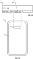
- FIGS. 1A and 1B are diagrams of an example electronic device 100 with a display 110 and a light sensor 120.
- FIG. 1A illustrates a front perspective view of the electronic device 100.
- FIG. 1B illustrates an example cross section view of the electronic device 100.
- the electronic device 100 may be, for example, a smart phone, a television, a smart watch, or a handheld game console.
- the display 110 includes an array of light-emitting pixels. In operation, the display 110 can display an image by illuminating the light-emitting pixels.
- the display 110 may be, for example, an active matrix organic light-emitting diode (OLED), or a light-emitting diode (LED) liquid crystal display (LCD).
- OLED active matrix organic light-emitting diode
- LED light-emitting diode
- LCD liquid crystal display
- the electronic device 100 includes the light sensor 120 adjacent to the display 110. For example, the light sensor 120 may be located behind the display 110 from the front perspective view of the electronic device 100.
- An OLED display generally includes an array of pixels, each pixel including one or more OLEDs.
- An OLED display is typically driven by driver circuits including a row driver and a column driver.
- the row driver e.g., a scan driver
- the column driver e.g., a data driver
- the pixel circuits generate electric current that corresponds to the driving voltage.
- the pixel circuits provide the current to OLEDs of the pixel, enabling the selected OLEDs to emit light, and presenting an image on the display.
- Signal lines such as scan lines and data lines may be used in controlling the pixels to display images on the display.
- the light sensor 120 can receive ambient light 130 through the display 110.
- the light sensor 120 can be, for example, an ambient light sensor (ALS) or a red-green-blue (RGB) color sensor.
- ALS ambient light sensor
- RGB red-green-blue
- the light sensor 120 can receive electromagnetic energy in a range of bands of the electromagnetic spectrum.
- the electronic device 100 can include more than one light sensor 120.
- An ALS sensor can measure ambient light to adapt display brightness.
- An ALS can detect overall light intensity surrounding the electronic device 100. Based on the detected light intensity, the display 110 can adjust brightness and contrast. Adjusting brightness and contrast can improve visibility of images on the display 110 and can improve battery life of the electronic device 100.
- An RGB sensor can measure ambient color to adapt display color.
- An RGB sensor includes individual sensors that can detect red, green, and blue light.
- An RGB sensor can detect a proportion of each color in the light surrounding the electronic device 100. Based on detected color, the display 110 can adjust color balance. Adjusting color balance can improve visibility and quality of images on the display 110.
- This specification describes burn-in compensation techniques primarily with reference to luminance of light emitted by pixels, as measured by an ALS sensor. However, the techniques described can also be applied to luminance of individual subpixels, e.g., RGB subpixels, as measured by an RGB sensor.
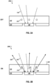
- FIGS. 2A and 2B show cross section views 200a, 200b of the example display 110 and the light sensor 120 in an emission-off (“OFF") condition and an emission-on (“ON”) condition, respectively.
- the sensor 120 receives ambient light 130 through adjacent pixels 210 of the display 110.
- FIG. 2A shows a cross section view of the example display 110 and the light sensor 120 in the OFF condition.
- the adjacent pixels 210 emit no light.
- the sensor 120 receives only the ambient light 130.
- FIG. 2B shows a cross section view of the example display 110 and the light sensor 120 in the ON condition.
- the adjacent pixels 210 emit light.
- the projected light 230 projects outward from a surface 220 of the display 110, such that an image is shown on the display 110.
- the reflected light 240 reflects away from the surface 220 of the display 110.
- the reflected light 240 can reflect off of one or more internal layers of the display 110.
- Some of the reflected light 240 may be received by the sensor 120.
- the sensor 120 receives both ambient light 130 and reflected light 240.
- the reflected light 240 from the adjacent pixels 210 is a fraction of the total light emitted from the adjacent pixels 210.
- the intensity, or luminance, of the reflected light 240 may be indicative of the intensity of light emitted from the pixel 210.
- the luminance of the reflected light 240 may be proportional to the luminance of light emitted from the pixels 210.
- the sensor 120 can receive and measure a luminance of received light while in the OFF condition, and while in the ON condition.
- the difference between received luminance while in the OFF condition and the ON condition is the luminance of the reflected light, and therefore indicates the luminance of light emitted from the pixels 210.
- the luminance of light emitted from the pixels 210, and therefore the luminance of reflected light may change over time due to degradation, or burn-in.
- the luminance of light emitted from the pixels 210, and therefore the luminance of reflected light may also change over time due overcompensation or undercompensation by a burn-in model.
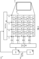
- FIG. 3 is a diagram of a display system 300 of the electronic display 110.
- the display system 300 is an OLED display system that includes an array 312 of light-emitting pixels. Each light-emitting pixel includes an OLED.
- the OLED display is driven by drivers including scan/emission drivers 308 and data drivers 310.
- the scan/emission drivers 308 selects a row of pixels in the display
- the data drivers 310 provide data signals (e.g. voltage data) to the pixels in the selected row to light the selected OLEDs according to the image data.
- Signal lines such as scan lines, emission lines, and data lines may be used in controlling the pixels to display images on the display.
- FIG. 3 illustrates the display system having the scan/emission drivers on one side of the system but the drivers can be placed on both left and right sides of the display improving the driving performance (e.g. speed).
- the display system 300 includes the pixel array 312 that includes a plurality of light-emitting pixels, e.g., the pixels P11 through P43.
- a pixel is a small element on a display that can change color based on the image data supplied to the pixel.
- Each pixel within the pixel array 312 can be addressed separately to produce various intensities of color.
- the pixel array 312 extends in a plane and includes rows and columns. A row extends horizontally across the array. For example, the first row of the pixel array 312 includes pixels P11, P12, and P13.
- a column extends vertically down the display. For example, the first column of the pixel array 312 includes pixels P11, P21, P31, and P41. Only a few pixels are shown in FIG. 3 for simplicity. In practice, there may be several million pixels in the pixel array 312. Greater numbers of pixels can result in higher image resolution.
- the display system 300 includes scan/emission drivers 308 and data drivers 310.
- the scan/emission drivers 308 are integrated, i.e., stacked, row line drivers that supply signals to rows of the pixel array 312.
- the scan/emission drivers 308 supply scan signals S1 to S4, and emission signals E1 to E4, to the rows of pixels.
- the data drivers 310 supply signals to columns of the pixel array 312.
- the data drivers 310 supply data signals D1 to D4 to the columns of pixels.
- Each pixel in the pixel array 312 is addressable by a horizontal scan line and emission line, and a vertical data line.
- the pixel P11 is addressable by the scan line S1, the emission line E1, and the data line D1.
- the pixel P32 is addressable by the scan line S3, the emission line E3, and the data line D2.
- the display system 300 includes a display driver integrated circuit (DDIC) 306 that receives display input data 302 from a system-on-chip (SoC) 304.
- the DDIC 306 may include a graphic controller and a timing controller.
- the DDIC 306 generates the timing of the signals for delivery to the display.
- the DDIC 306 provides the input signals (e.g. clock signals, start pulses) to the scan/emission drivers 308, and the image data to the data drivers 310.
- the scan/emission drivers 308 and the data drivers 310 provide signals to the pixels enabling the pixels reproduce the image on the display screen.
- the scan/emission drivers 308 and the data drivers 310 provide the signals to the pixels via the scan lines, the emission lines, and the data lines.
- the scan/emission drivers 308 select a scan line and control the emission operation of the pixels.
- the data drivers 310 provides data signals to the pixels addressable by the selected scan line to light the selected OLEDs according to the image data.
- FIG. 3 illustrates an OLED display
- the technique for burn-in compensation may be applied to any flat panel display that includes an array of pixels.
- the technique for burn-in compensation may be applied to light-emitting diode (LED) liquid crystal displays (LCD) and plasma electronic displays (PDP).
- LED light-emitting diode
- LCD liquid crystal displays
- PDP plasma electronic displays
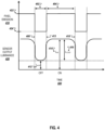
- FIG. 4 is an example operating timing diagram for the example display 110 with the light sensor 120.
- FIG. 4 shows a graph of pixel emission 410, and a graph of sensor output luminance 420, over time 430.
- the pixel emission 410 can represent operation, e.g., a driving voltage, of one of the pixels 210 that is adjacent to the sensor 120.
- the pixel emission 410 can also represent operation of a row of multiple pixels 210 that are adjacent to the sensor 120.
- the pixel emission 410 shows the pixel alternating between a high value 422 and a low value 424.
- the pixel turns off for a duration of an emission-off period 402, illustrated by the pixel emission 410 dropping from the high value 422 to the low value 424.
- the pixel emits no light.
- the pixel turns on for a duration of an emission-on period 404, illustrated by the pixel emission 410 rising to the high value 422.
- the pixel emits light.
- the pixel turns off again.
- the pixel may turn on an off at designated intervals, e.g., corresponding to a frame rate of the display system.
- the display system may program the pixel with image data for a next frame.
- the sensor output luminance 420 can represent output of the sensor 120.
- the sensor 120 can measure and output luminance (L) of received light over time 430. During the emission-off period 402, the sensor 120 only receives ambient light. The sensor 120 therefore measures ambient luminance (L amb ) 412 of received light during the emission-off period 402.
- Reflected OLED luminance L OLED 416 is a luminance of light internally reflected from the adjacent pixels and received by the sensor 120 during the emission-on period 404.
- the sensor 120 measures a total luminance L tot 414 of received light during the emission-on period 404 that is a combination of ambient luminance L amb 412 and reflected OLED luminance L OLED 416.
- a display system can calculate the reflected OLED luminance L OLED 416.
- the reflected OLED luminance L OLED 416 may be a function of pixel intensity, e.g., may be proportional to pixel luminance.
- the display system can estimate pixel luminance.
- FIG. 5 is a diagram of an example system 500 for display burn-in compensation.
- the system 500 compensates an image to be shown on a display, e.g., the display 110.
- the system 500 includes the display 110 with the sensor 120, an OLED model error calculator (OMEC) 520, and a burn-in compensator 524.
- the OMEC 520 includes an OLED reference calculator 510 and an error accumulator 518.
- the burn-in compensator 524 includes a burn-in model 525.
- the OMEC 520, the burn-in compensator 524, or both, can be components of the DDIC or the SoC, e.g., the DDIC 306 or the SoC 304 of the display system 200.
- the burn-in model 525 is a model of expected degradation over time for the pixels of the display 110.
- the burn-in model 525 can include expected average pixel and/or subpixel luminance as a function of time, e.g., time of operation. In general, pixel luminance is expected to decrease over time.
- the burn-in model 525 can be pre-programmed and may be based on historical trends and statistical data.
- the burn-in compensator 524 can compensate the display 110 according to the burn-in model 525. For example, at a certain time of operation, the burn-in model 525 may predict that pixels of the display 110 will be 3% dimmer, on average, than the initial programmed luminance level. The burn-in compensator 524 can therefore provide a compensating signal COMP 526 to the display 110 to increase the luminance of the pixels by 3%.
- the compensating signal COMP 526 may include, for example, an adjustment to the driving voltage provided by the DDIC 306. The adjusted driving voltage causes the average pixel luminance to rise 3%, returning to the initial programmed luminance level.
- pixel degradation might not follow the burn-in model 525 exactly.
- the burn-in model 525 may be based on an expected usage time, expected environmental conditions, e.g., temperature, and other factors. Actual conditions of usage may differ from the expected conditions. Thus, actual pixel luminance at a certain time may be more or less than predicted by the burn-in model 525. The difference between predicted pixel luminance and actual pixel luminance can be considered luminance error.
- the burn-in compensator 524 may overcompensate or undercompensate the display 110. If the burn-in rate is less than predicted by the burn-in model 525, the burn-in compensator 524 will likely overcompensate the display 110. This can result in actual pixel luminance exceeding the programmed pixel luminance. If the burn-in rate is greater than predicted by the burn-in model 525, the burn-in compensator 524 will likely undercompensate the display 110. This can result in actual pixel luminance being less than the programmed luminance.
- the system 500 can mitigate undercompensation and overcompensation of burn-in.
- the system 500 can measure errors between expected pixel luminance and actual pixel luminance, and can apply a correction to the burn-in model 525.
- the OLED reference calculator 510 can calculate a reference luminance L REF 514.
- the reference luminance L REF 514 can be an expected reflected OLED luminance, e.g., a luminance level of reflected light that the sensor 120 is expected to receive at a given time. Since the reflected light from each pixel is a fraction of the total light emitted from the pixel, the reference luminance L REF 514 is a luminance value that is less than the expected pixel luminance.
- the OLED reference calculator 510 can be calibrated to the particular display 110. For example, upon assembly, the pixels may emit light at a known, programmed, luminance, given certain display brightness values (DBVs) 502, RGB values 504, and environmental conditions, e.g., ambient temperature (TEMP) 506.
- the sensor 120 can measure the total luminance L tot 414 and the ambient luminance L amb 412.
- the OMEC 520 can collect, from the sensor 120, data indicating the total luminance L tot 414 and the ambient luminance L amb 412.
- the OMEC 520 can compare the total luminance L tot 414 to the ambient luminance L amb 412 to calculate the reflected luminance for the known conditions.
- the OLED reference calculator 510 can then be calibrated to correlate the calculated reflected luminance with the known emitted luminance.
- the OLED reference calculator 510 can calculate the reference luminance L REF 514 based on a number of factors. For example, the OLED reference calculator 510 can calculate the reference luminance L REF 514 based on programmed DBV 502, RGB values 504, and ambient temperature 506.
- the sensor 120 collects sensor data 505.
- the sensor data 505 can include luminance of received light over time, as shown in FIG. 4 .
- the sensor data 505 can also include the total luminance L tot 414, measured during emission-on periods, and the ambient luminance L amb 412, measured during emission-off periods.
- the OMEC 520 can compare the total luminance L tot 414 to the ambient luminance L amb 412 to calculate the reflected OLED luminance L OLED 416. The OMEC 520 can then compare the reflected OLED luminance L OLED 416 to the reference luminance L REF 514, e.g., by subtracting L REF 514 from L OLED 416, to calculate reflected luminance error ⁇ L 516.
- the reflected luminance error ⁇ L 516 represents a difference between the luminance of light internally reflected from the adjacent pixels and received by the sensor during the emission-on period, and the reference luminance L REF 514.
- the reflected luminance error ⁇ L 516 can be a positive value or a negative value.
- a positive ⁇ L 516 can indicate overcompensation, while a negative ⁇ L 516 can indicate undercompensation.
- the error accumulator 518 can accumulate and average the reflected luminance error ⁇ L 516 over a time period 508.
- the time period 508 can be, for example, a number of hours, days, weeks, or months.
- the error accumulator 518 outputs an average error ⁇ L avg .
- the OMEC 520 can compare the average error ⁇ L avg to a luminance threshold error ⁇ L thr .
- the luminance threshold error ⁇ L thr can be, for example, an error value that may cause visible display effects, e.g., +/-5% of the programmed luminance.
- the OMEC 520 may determine that the average error ⁇ L avg between the luminance of light internally reflected from the adjacent pixels and the reference luminance exceeds the threshold error ⁇ L thr . If the average error ⁇ L avg equals or exceeds the luminance threshold error ⁇ L thr , the OMEC 520 can output the average error ⁇ L avg to the burn-in compensator 524.
- the burn-in compensator 524 updates the burn-in model 525 based on the average error ⁇ L avg .
- the burn-in compensator 524 can update the burn-in model 525 by offsetting the burn-in model 525 by a correction factor.
- the correction factor may be, for example, an additive inverse of the average error ⁇ L avg .For example, the average error ⁇ L avg may be +5.1%.
- the burn-in compensator 524 may update the burn-in model 525 by offsetting the burn-in model 525 by -5.1%, to return the pixel luminance to the programmed value.
- the burn-in compensator 524 may update the burn-in model 525 for all of the pixels of the display 110. For example, in smaller displays, the display system may assume that burn-in rates for all of the pixels of the array are approximately equal. Thus, though the sensor 120 might only be adjacent to a fraction of pixels of the array, the burn-in model update can be applied to all of the pixels of the display.
- the burn-in compensator 524 may update the burn-in model 525 for a selection of the pixels of the display 110.
- some displays may have more than one sensor, e.g., a first sensor adjacent to a top region of the display and a second sensor adjacent to a bottom region of a display.
- the burn-in compensator 524 may update the burn-in model 525 for pixels of the display that are nearer to the first sensor with model updates calculated using sensor data 505 from the first sensor.
- the burn-in compensator 524 may update the burn-in model 525 for pixels of the display that are nearer to the second sensor with model updates calculated using sensor data 505 from the second sensor.
- the OMEC 520 may continuously calculate luminance error. In some examples, the OMEC 520 may calculate luminance error at designated time intervals or in response to an event. For example, the OMEC may calculate luminance error at an interval of once per hour, once per day, or once per week. In some examples, the OMEC may calculate luminance error in response to the display turning on, or in response to receiving input from a user.
- FIG. 6 is an example graph 600 of luminance error over time for the display 110 with burn-in compensation. Specifically, FIG. 6 shows a graph of average error ⁇ L avg 620 over time 630.
- the burn-in compensator 524 maintains the average error ⁇ L avg 620 between a positive update threshold 604 and a negative update threshold 608.
- the positive update threshold 604 and/or the negative update threshold 608 may be, for example, the luminance threshold error ⁇ L thr of FIG. 5 .
- the burn-in compensator 524 prevents the average error ⁇ L avg 620 from reaching either a positive visible threshold error 602 or a negative visible threshold error 610.
- the positive update threshold 604, the negative update threshold 608, the positive visible threshold error 602, and the negative visible threshold error 610 can each be a percentage error of the programmed luminance.
- the positive update threshold 604 and the negative update threshold 608 may be +1.0% and -1.0%, respectively.
- the positive visible threshold error 602 and the negative visible threshold error 610 may be +5.0% and -5.0%, respectively.
- the average error ⁇ L avg 620 is at a value of zero error 606.
- the reflected OLED luminance L OLED 416 is equal to the reference luminance L REF 514, on average.
- the display operates for a period of time 630.
- the time 630 may be, for example, multiple weeks or months of operation.
- the average error ⁇ L avg 620 increases.
- the average error ⁇ L avg 620 may increase, for example, due to overcompensation of burn-in.
- the average error ⁇ L avg 620 reaches the positive update threshold 604.
- the OMEC 520 outputs the average error ⁇ L avg 620 to the burn-in compensator 524.
- the burn-in compensator 524 updates the burn-in model 525 based on the average error ⁇ L avg 620, e.g., by offsetting the burn-in model by a correction factor of (- ⁇ L avg ).
- the burn-in compensator 524 updates the burn-in model 525, the average error ⁇ L avg 620 drops 622 to zero error 606.
- the average error ⁇ L avg 620 is at a value of zero error 606.
- the reflected OLED luminance L OLED 416 is equal to the reference luminance L REF 514, on average.
- the average error ⁇ L avg 620 decreases.
- the average error ⁇ L avg 620 may decrease, for example, due to undercompensation of burn-in.
- the average error ⁇ L avg 620 reaches the negative update threshold 608.
- the OMEC 520 outputs the average error ⁇ L avg 620 to the burn-in compensator 524.
- the burn-in compensator 524 updates the burn-in model 525 based on the average error ⁇ L avg 620, e.g., by offsetting the burn-in model by the correction factor of (- ⁇ L avg ).
- ⁇ L avg has a negative error value
- (- ⁇ L avg ) has a positive value that is the additive inverse of ⁇ L avg .
- the process for burn-in compensation can be used throughout display operation to maintain consistent pixel brightness and color in displays.
- the system 500 can continue to measure luminance error and to update the burn-in model when luminance error reaches designated thresholds.
- the techniques described can improve display quality and can increase OLED lifetime.
- Embodiments of the subject matter and the functional operations described in this specification can be implemented in any suitable electronic device such as a personal computer, a mobile telephone, a smart phone, a smart watch, a smart TV, a mobile audio or video player, a game console, or a combination of one or more of these devices.
- a personal computer a mobile telephone, a smart phone, a smart watch, a smart TV, a mobile audio or video player, a game console, or a combination of one or more of these devices.
- the electronic device may include various components such as a memory, a processor, a display, and input/output units.
- the input/output units may include, for example, a transceiver which can communicate with the one or more networks to send and receive data.
- the display may be any suitable display including, for example, a cathode ray tube (CRT), liquid crystal display (LCD), or light-emitting diode (LED) display, for displaying images.
- CTR cathode ray tube
- LCD liquid crystal display
- LED light-emitting diode
- implementations of the systems and techniques described here can be realized in digital electronic circuitry, integrated circuitry, specially designed ASICs (application specific integrated circuits), computer hardware, firmware, software, and/or combinations thereof.
- ASICs application specific integrated circuits
- These various implementations can include implementation in one or more computer programs that are executable and/or interpretable on a programmable system including at least one programmable processor, which may be special or general purpose, coupled to receive data and instructions from, and to transmit data and instructions to, a storage system, at least one input device, and at least one output device.
- Embodiments may be implemented as one or more computer program products, e.g., one or more modules of computer program instructions encoded on a computer readable medium for execution by, or to control the operation of, data processing apparatus.
- the computer readable medium may be a machine-readable storage device, a machine-readable storage substrate, a memory device, a composition of matter effecting a machine-readable propagated signal, or a combination of one or more of them.
- data processing apparatus encompasses all apparatus, devices, and machines for processing data, including by way of example a programmable processor, a computer, or multiple processors or computers.
- the apparatus may include, in addition to hardware, code that creates an execution environment for the computer program in question, e.g., code that constitutes processor firmware, a protocol stack, a database management system, an operating system, or a combination of one or more of them.
- a propagated signal is an artificially generated signal, e.g., a machine-generated electrical, optical, or electromagnetic signal that is generated to encode information for transmission to suitable receiver apparatus.
- a computer program (also known as a program, software, software application, script, or code) may be written in any form of programming language, including compiled or interpreted languages, and it may be deployed in any form, including as a standalone program or as a module, component, subroutine, or other unit suitable for use in a computing environment.
- a computer program does not necessarily correspond to a file in a file system.
- a program may be stored in a portion of a file that holds other programs or data (e.g., one or more scripts stored in a markup language document), in a single file dedicated to the program in question, or in multiple coordinated files (e.g., files that store one or more modules, sub programs, or portions of code).
- a computer program may be deployed to be executed on one computer or on multiple computers that are located at one site or distributed across multiple sites and interconnected by a communication network.
- processors suitable for the execution of a computer program include, by way of example, both general and special purpose microprocessors, and any one or more processors of any kind of digital computer.
- a processor will receive instructions and data from a read only memory or a random access memory or both.
- Elements of a computer may include a processor for performing instructions and one or more memory devices for storing instructions and data.
- a computer will also include, or be operatively coupled to receive data from or transfer data to, or both, one or more mass storage devices for storing data, e.g., magnetic, magneto optical disks, or optical disks.
- mass storage devices for storing data, e.g., magnetic, magneto optical disks, or optical disks.
- Computer-readable media suitable for storing computer program instructions and data include all forms of non-volatile memory, media and memory devices, including by way of example semiconductor memory devices, e.g., EPROM, EEPROM, and flash memory devices; magnetic disks, e.g., internal hard disks or removable disks; magneto optical disks; and CD ROM and DVD-ROM disks.
- the processor and the memory may be supplemented by, or incorporated in, special purpose logic circuitry.
Landscapes
- Engineering & Computer Science (AREA)
- Physics & Mathematics (AREA)
- Computer Hardware Design (AREA)
- General Physics & Mathematics (AREA)
- Theoretical Computer Science (AREA)
- Control Of Indicators Other Than Cathode Ray Tubes (AREA)
- Electroluminescent Light Sources (AREA)
- Control Of El Displays (AREA)
Claims (9)
- Verfahren zum Kompensieren eines Bildes, das auf einer Anzeige (110) angezeigt werden soll, umfassend eine Anzeigefläche (220), eine Anordnung von lichtemittierenden Pixeln und einen Sensor, der benachbart zu der Anzeige angeordnet ist, um sich in einer Vorderansicht hinter der Anzeige zu befinden; wobei das Verfahren Folgendes umfasst:Antreiben der Anzeige mit Antriebsspannungssignalen, die gemäß einem Einbrennmodell kompensiert werden, das die vorausgesagte Pixelverschlechterung im Laufe der Zeit darstellt;Sammeln einer Leuchtdichte von Licht, das durch den Sensor während einer Emissions-An-Periode empfangen wird, während der benachbart zum Sensor (120) lichtemittierende Pixel (210) Licht gemäß den kompensierten Antriebsspannungssignalen emittieren, von dem Sensor, wobei der Sensor während der Emissionsperiode sowohl ein Umgebungslicht (130), das durch die Anzeigefläche (220) hindurchtritt, als auch das durch die benachbarten lichtemittierenden Pixel (210) emittierte und intern von der Anzeigefläche (220) weg reflektierte Licht empfängt;Sammeln einer Leuchtdichte von Licht, das durch den Sensor während einer Emissions-Aus-Periode empfangen wird, während der die benachbarten lichtemittierenden Pixel kein Licht emittieren, von dem Sensor, sodass der Sensor (120) nur das Umgebungslicht empfängt;Berechnen einer Leuchtdichte von Licht, das intern von der Anzeigefläche (220) weg reflektiert und durch den Sensor während der Emissions-An-Periode empfangen wird, durch Vergleichen der Leuchtdichte des Lichts, das durch den Sensor während der Emissions-An-Periode angezeigt wird, mit der Leuchtdichte des Lichts, das durch den Sensor während der Emissions-Aus-Periode empfangen wird;Bestimmen einer Referenzleuchtdichte, die auf dem Einbrennmodell basiert, wobei die Referenzleuchtdichte eine erwartete Leuchtdichte von Licht umfasst, das intern von der Anzeigefläche (220) reflektiert wird und von dem Sensor (120) empfangen werden soll;Bestimmen, ob ein Fehler zwischen der Leuchtdichte von Licht, das intern von der Anzeigefläche (22) weg reflektiert und durch den Sensor während der Emissions-An-Periode empfangen wird, und der Referenzleuchtdichte basierend auf dem Einbrennmodell gleich einem Schwellenwertfehler ist oder diesen überschreitet, wobei der Fehler einen Fehler in dem Einbrennmodell angibt;als Reaktion auf das Bestimmen, dass der Fehler gleich dem Schwellenwert ist oder diesen überschreitet, Aktualisieren des Einbrennmodells basierend auf dem Fehler;
undAnpassen der Antriebsspannungssignale zum Antreiben der lichtemittierenden Pixel basierend auf dem aktualisierten Einbrennmodell, um den Fehler zu verringern. - Verfahren nach Anspruch 1, wobei die Anordnung von lichtemittierenden Pixeln eine Anordnung von organischen Leuchtdioden (organic light-emitting diodes, OLED) umfasst.
- Verfahren nach Anspruch 1, wobei das Aktualisieren des Einbrennmodells das Anpassen des Einbrennmodells um einen Korrekturfaktor umfasst.
- Verfahren nach Anspruch 3, wobei der Korrekturfaktor einen additiven Inversen des Fehlers umfasst.
- Verfahren nach einem der Ansprüche 1-4, wobei der Sensor ein Umgebungslichtsensor oder ein Rot-Grün-Blau-Sensor (red-green-blue, RGB) ist.
- Verfahren nach einem der Ansprüche 1-5, wobei das Bestimmen, dass ein Fehler zwischen der Leuchtdichte von Licht, das intern von der Anzeigefläche (220) weg reflektiert und durch den Sensor während der Emissions-An-Periode empfangen wird, und der Referenzleuchtdichte gleich einem Schwellenwertfehler ist oder diesen überschreitet, umfassend:Akkumulieren des Fehlers über eine bestimmte Zeitspanne;Mittelwertbilden des Fehlers; undVergleichen des gemittelten Fehlers mit dem Schwellenwertfehler.
- Verfahren nach einem der Ansprüche 1-6, wobei das Anpassen der Antriebsspannungssignale das Anpassen der Antriebsspannungssignale für alle lichtemittierenden Pixel der Anordnung umfasst.
- Anzeigesystem, umfassend:eine Anzeige (110), umfassend eine Anzeigefläche (220);eine Anordnung von lichtemittierenden Pixeln, die während des Betriebs Licht als Reaktion auf ein Antriebsspannungssignal emittieren;einen Sensor, der benachbart zu der Anzeige angeordnet ist, um sich in einer Vorderansicht hinter der Anzeige zu befinden; undein Steuermodul in elektrischer Kommunikation mit der Anordnung von lichtemittierenden Pixeln, wobei das Steuermodul dazu programmiert ist, ein Verfahren nach einem der vorhergehenden Ansprüche durchzuführen.
- Nichttransitorisches computerlesbares Medium, das Anweisungen enthält, die, wenn sie auf einer Datenverarbeitungsvorrichtung in Kommunikation mit einem Anzeigesystem nach Anspruch 8 oder auf dem Steuermodul des Anzeigesystems nach Anspruch 8 ausgeführt werden, die Datenverarbeitungsvorrichtung oder das Steuermodul veranlassen, ein Verfahren nach einem der Ansprüche 1 bis 7 durchzuführen.
Applications Claiming Priority (1)
| Application Number | Priority Date | Filing Date | Title |
|---|---|---|---|
| PCT/US2020/015072 WO2021150249A1 (en) | 2020-01-24 | 2020-01-24 | Display burn-in compensation |
Publications (2)
| Publication Number | Publication Date |
|---|---|
| EP4004903A1 EP4004903A1 (de) | 2022-06-01 |
| EP4004903B1 true EP4004903B1 (de) | 2025-03-05 |
Family
ID=69724122
Family Applications (1)
| Application Number | Title | Priority Date | Filing Date |
|---|---|---|---|
| EP20707953.4A Active EP4004903B1 (de) | 2020-01-24 | 2020-01-24 | Kompensation des einbrennens einer anzeige |
Country Status (4)
| Country | Link |
|---|---|
| US (1) | US11893933B2 (de) |
| EP (1) | EP4004903B1 (de) |
| CN (1) | CN114341969B (de) |
| WO (1) | WO2021150249A1 (de) |
Families Citing this family (4)
| Publication number | Priority date | Publication date | Assignee | Title |
|---|---|---|---|---|
| CN115331625B (zh) * | 2022-08-31 | 2025-10-03 | 京东方科技集团股份有限公司 | 模型调整方法、装置、显示装置和存储介质 |
| EP4721041A1 (de) * | 2023-05-26 | 2026-04-08 | Qualcomm Incorporated | Plattenalterungsbedingungsaufzeichnungsstrategie für oled-alterungsschutz |
| KR20260021617A (ko) * | 2023-06-09 | 2026-02-13 | 퀄컴 인코포레이티드 | 유기 발광 다이오드에 대한 지역적 노화방지 모니터링 |
| KR20260000044A (ko) * | 2024-06-24 | 2026-01-02 | 삼성디스플레이 주식회사 | 표시 장치, 이를 포함하는 전자 장치, 및 이의 구동 방법 |
Citations (1)
| Publication number | Priority date | Publication date | Assignee | Title |
|---|---|---|---|---|
| US9622326B1 (en) * | 2015-12-18 | 2017-04-11 | Amazon Technologies, Inc. | Method and device for determining emitted light intensity level |
Family Cites Families (12)
| Publication number | Priority date | Publication date | Assignee | Title |
|---|---|---|---|---|
| GB0318613D0 (en) * | 2003-08-08 | 2003-09-10 | Koninkl Philips Electronics Nv | Electroluminescent display devices |
| JP2007501953A (ja) * | 2003-08-08 | 2007-02-01 | コーニンクレッカ フィリップス エレクトロニクス エヌ ヴィ | エレクトロルミネセント表示装置 |
| WO2007110810A1 (en) * | 2006-03-28 | 2007-10-04 | Koninklijke Philips Electronics N.V. | Integrated device having an array of photodetectors and an array of sample sites |
| KR100902219B1 (ko) * | 2007-12-05 | 2009-06-11 | 삼성모바일디스플레이주식회사 | 유기전계발광 표시장치 |
| US20100201275A1 (en) | 2009-02-06 | 2010-08-12 | Cok Ronald S | Light sensing in display device |
| EP2299427A1 (de) * | 2009-09-09 | 2011-03-23 | Ignis Innovation Inc. | Antriebssystem für Aktivmatrixanzeigen |
| GB201022138D0 (en) | 2010-12-31 | 2011-02-02 | Barco Nv | Display device and means to measure and isolate the ambient light |
| US8451437B2 (en) * | 2011-02-17 | 2013-05-28 | Global Oled Technology Llc | Electroluminescent light output sensing for variation detection |
| US20160042676A1 (en) * | 2014-08-06 | 2016-02-11 | Samsung Display Co., Ltd. | Apparatus and method of direct monitoring the aging of an oled display and its compensation |
| CN105096834B (zh) * | 2015-08-26 | 2017-05-17 | 京东方科技集团股份有限公司 | 一种有源矩阵有机发光二极管显示装置及其亮度补偿方法 |
| US10545242B2 (en) * | 2016-09-14 | 2020-01-28 | Apple Inc. | Systems and methods for in-frame sensing and adaptive sensing control |
| US11410611B2 (en) * | 2018-08-10 | 2022-08-09 | Ams Ag | Ambient light sensor system |
-
2020
- 2020-01-24 EP EP20707953.4A patent/EP4004903B1/de active Active
- 2020-01-24 US US16/967,222 patent/US11893933B2/en active Active
- 2020-01-24 CN CN202080060113.4A patent/CN114341969B/zh active Active
- 2020-01-24 WO PCT/US2020/015072 patent/WO2021150249A1/en not_active Ceased
Patent Citations (1)
| Publication number | Priority date | Publication date | Assignee | Title |
|---|---|---|---|---|
| US9622326B1 (en) * | 2015-12-18 | 2017-04-11 | Amazon Technologies, Inc. | Method and device for determining emitted light intensity level |
Also Published As
| Publication number | Publication date |
|---|---|
| US11893933B2 (en) | 2024-02-06 |
| CN114341969B (zh) | 2024-10-15 |
| WO2021150249A1 (en) | 2021-07-29 |
| CN114341969A (zh) | 2022-04-12 |
| EP4004903A1 (de) | 2022-06-01 |
| US20220366846A1 (en) | 2022-11-17 |
Similar Documents
| Publication | Publication Date | Title |
|---|---|---|
| EP4004903B1 (de) | Kompensation des einbrennens einer anzeige | |
| CN111754935B (zh) | 显示面板的补偿方法、装置及显示装置 | |
| CN108122532B (zh) | 有机发光显示装置及其驱动方法 | |
| KR102049089B1 (ko) | 표시 장치의 색 보상 장치 및 방법 | |
| US9959807B2 (en) | Organic light-emitting display device and driving method thereof | |
| US10157568B2 (en) | Image processing method, image processing circuit, and organic light emitting diode display device using the same | |
| US11328650B2 (en) | Driver, display device and optical compensation method | |
| KR102071056B1 (ko) | 표시 장치 및 그의 영상 보상 방법 | |
| KR102853275B1 (ko) | 표시 장치 및 표시 장치의 제어 방법 | |
| US20210193011A1 (en) | Color shift compensation method, color shift compensation system and display panel | |
| KR20170137456A (ko) | 모듈형 디스플레이 장치, 이를 포함하는 디스플레이 장치 및 그 제어 방법 | |
| US20220157237A1 (en) | Compensation systems and methods for oled display degradation | |
| US11276347B2 (en) | Compensation systems and methods for display OLED degradation | |
| KR102135926B1 (ko) | 유기 발광 다이오드 표시 장치 및 그의 보상 방법 | |
| US10043438B2 (en) | Display device and method of driving the same with pixel shifting compensation data | |
| US11741867B2 (en) | Display device for preventing deterioration and method of compensating thereof | |
| JP5124939B2 (ja) | 自発光表示装置、変換テーブル更新装置及びプログラム | |
| JP2007164003A (ja) | 自発光表示装置、画像処理装置、点灯時間長制御装置及びプログラム | |
| JP2007163712A (ja) | 表示パネル、自発光表示装置、階調値/劣化率変換テーブル更新装置、入力表示データ補正装置及びプログラム | |
| JP4830495B2 (ja) | 自発光表示装置、変換テーブル更新装置及びプログラム | |
| KR102623356B1 (ko) | 유기 발광 표시 장치 및 그의 구동 방법 | |
| JP2007206464A (ja) | 自発光表示装置、見積もり劣化情報修正装置、入力表示データ補正装置及びプログラム | |
| US12205544B2 (en) | Display device | |
| JP2007240798A (ja) | 自発光表示装置、階調値/劣化量変換テーブル更新装置、入力表示データ補正装置及びプログラム | |
| US11842680B2 (en) | Semiconductor device and electronic apparatus |
Legal Events
| Date | Code | Title | Description |
|---|---|---|---|
| STAA | Information on the status of an ep patent application or granted ep patent |
Free format text: STATUS: UNKNOWN |
|
| STAA | Information on the status of an ep patent application or granted ep patent |
Free format text: STATUS: THE INTERNATIONAL PUBLICATION HAS BEEN MADE |
|
| PUAI | Public reference made under article 153(3) epc to a published international application that has entered the european phase |
Free format text: ORIGINAL CODE: 0009012 |
|
| STAA | Information on the status of an ep patent application or granted ep patent |
Free format text: STATUS: REQUEST FOR EXAMINATION WAS MADE |
|
| 17P | Request for examination filed |
Effective date: 20220228 |
|
| AK | Designated contracting states |
Kind code of ref document: A1 Designated state(s): AL AT BE BG CH CY CZ DE DK EE ES FI FR GB GR HR HU IE IS IT LI LT LU LV MC MK MT NL NO PL PT RO RS SE SI SK SM TR |
|
| DAV | Request for validation of the european patent (deleted) | ||
| DAX | Request for extension of the european patent (deleted) | ||
| STAA | Information on the status of an ep patent application or granted ep patent |
Free format text: STATUS: EXAMINATION IS IN PROGRESS |
|
| 17Q | First examination report despatched |
Effective date: 20240513 |
|
| GRAP | Despatch of communication of intention to grant a patent |
Free format text: ORIGINAL CODE: EPIDOSNIGR1 |
|
| STAA | Information on the status of an ep patent application or granted ep patent |
Free format text: STATUS: GRANT OF PATENT IS INTENDED |
|
| INTG | Intention to grant announced |
Effective date: 20241017 |
|
| GRAS | Grant fee paid |
Free format text: ORIGINAL CODE: EPIDOSNIGR3 |
|
| GRAA | (expected) grant |
Free format text: ORIGINAL CODE: 0009210 |
|
| STAA | Information on the status of an ep patent application or granted ep patent |
Free format text: STATUS: THE PATENT HAS BEEN GRANTED |
|
| P01 | Opt-out of the competence of the unified patent court (upc) registered |
Free format text: CASE NUMBER: APP_68228/2024 Effective date: 20241223 |
|
| AK | Designated contracting states |
Kind code of ref document: B1 Designated state(s): AL AT BE BG CH CY CZ DE DK EE ES FI FR GB GR HR HU IE IS IT LI LT LU LV MC MK MT NL NO PL PT RO RS SE SI SK SM TR |
|
| REG | Reference to a national code |
Ref country code: GB Ref legal event code: FG4D |
|
| REG | Reference to a national code |
Ref country code: CH Ref legal event code: EP |
|
| REG | Reference to a national code |
Ref country code: IE Ref legal event code: FG4D |
|
| REG | Reference to a national code |
Ref country code: DE Ref legal event code: R096 Ref document number: 602020047154 Country of ref document: DE |
|
| PG25 | Lapsed in a contracting state [announced via postgrant information from national office to epo] |
Ref country code: RS Free format text: LAPSE BECAUSE OF FAILURE TO SUBMIT A TRANSLATION OF THE DESCRIPTION OR TO PAY THE FEE WITHIN THE PRESCRIBED TIME-LIMIT Effective date: 20250605 |
|
| PG25 | Lapsed in a contracting state [announced via postgrant information from national office to epo] |
Ref country code: FI Free format text: LAPSE BECAUSE OF FAILURE TO SUBMIT A TRANSLATION OF THE DESCRIPTION OR TO PAY THE FEE WITHIN THE PRESCRIBED TIME-LIMIT Effective date: 20250305 |
|
| REG | Reference to a national code |
Ref country code: NL Ref legal event code: MP Effective date: 20250305 |
|
| PG25 | Lapsed in a contracting state [announced via postgrant information from national office to epo] |
Ref country code: ES Free format text: LAPSE BECAUSE OF FAILURE TO SUBMIT A TRANSLATION OF THE DESCRIPTION OR TO PAY THE FEE WITHIN THE PRESCRIBED TIME-LIMIT Effective date: 20250305 |
|
| REG | Reference to a national code |
Ref country code: LT Ref legal event code: MG9D |
|
| PG25 | Lapsed in a contracting state [announced via postgrant information from national office to epo] |
Ref country code: NO Free format text: LAPSE BECAUSE OF FAILURE TO SUBMIT A TRANSLATION OF THE DESCRIPTION OR TO PAY THE FEE WITHIN THE PRESCRIBED TIME-LIMIT Effective date: 20250605 |
|
| PG25 | Lapsed in a contracting state [announced via postgrant information from national office to epo] |
Ref country code: HR Free format text: LAPSE BECAUSE OF FAILURE TO SUBMIT A TRANSLATION OF THE DESCRIPTION OR TO PAY THE FEE WITHIN THE PRESCRIBED TIME-LIMIT Effective date: 20250305 |
|
| PG25 | Lapsed in a contracting state [announced via postgrant information from national office to epo] |
Ref country code: LV Free format text: LAPSE BECAUSE OF FAILURE TO SUBMIT A TRANSLATION OF THE DESCRIPTION OR TO PAY THE FEE WITHIN THE PRESCRIBED TIME-LIMIT Effective date: 20250305 |
|
| PG25 | Lapsed in a contracting state [announced via postgrant information from national office to epo] |
Ref country code: BG Free format text: LAPSE BECAUSE OF FAILURE TO SUBMIT A TRANSLATION OF THE DESCRIPTION OR TO PAY THE FEE WITHIN THE PRESCRIBED TIME-LIMIT Effective date: 20250305 Ref country code: GR Free format text: LAPSE BECAUSE OF FAILURE TO SUBMIT A TRANSLATION OF THE DESCRIPTION OR TO PAY THE FEE WITHIN THE PRESCRIBED TIME-LIMIT Effective date: 20250606 |
|
| REG | Reference to a national code |
Ref country code: AT Ref legal event code: MK05 Ref document number: 1773693 Country of ref document: AT Kind code of ref document: T Effective date: 20250305 |
|
| PG25 | Lapsed in a contracting state [announced via postgrant information from national office to epo] |
Ref country code: NL Free format text: LAPSE BECAUSE OF FAILURE TO SUBMIT A TRANSLATION OF THE DESCRIPTION OR TO PAY THE FEE WITHIN THE PRESCRIBED TIME-LIMIT Effective date: 20250305 |
|
| PG25 | Lapsed in a contracting state [announced via postgrant information from national office to epo] |
Ref country code: SE Free format text: LAPSE BECAUSE OF FAILURE TO SUBMIT A TRANSLATION OF THE DESCRIPTION OR TO PAY THE FEE WITHIN THE PRESCRIBED TIME-LIMIT Effective date: 20250305 |
|
| PG25 | Lapsed in a contracting state [announced via postgrant information from national office to epo] |
Ref country code: SM Free format text: LAPSE BECAUSE OF FAILURE TO SUBMIT A TRANSLATION OF THE DESCRIPTION OR TO PAY THE FEE WITHIN THE PRESCRIBED TIME-LIMIT Effective date: 20250305 |
|
| PG25 | Lapsed in a contracting state [announced via postgrant information from national office to epo] |
Ref country code: PT Free format text: LAPSE BECAUSE OF FAILURE TO SUBMIT A TRANSLATION OF THE DESCRIPTION OR TO PAY THE FEE WITHIN THE PRESCRIBED TIME-LIMIT Effective date: 20250707 |
|
| PG25 | Lapsed in a contracting state [announced via postgrant information from national office to epo] |
Ref country code: PL Free format text: LAPSE BECAUSE OF FAILURE TO SUBMIT A TRANSLATION OF THE DESCRIPTION OR TO PAY THE FEE WITHIN THE PRESCRIBED TIME-LIMIT Effective date: 20250305 Ref country code: IT Free format text: LAPSE BECAUSE OF FAILURE TO SUBMIT A TRANSLATION OF THE DESCRIPTION OR TO PAY THE FEE WITHIN THE PRESCRIBED TIME-LIMIT Effective date: 20250305 |
|
| PG25 | Lapsed in a contracting state [announced via postgrant information from national office to epo] |
Ref country code: AT Free format text: LAPSE BECAUSE OF FAILURE TO SUBMIT A TRANSLATION OF THE DESCRIPTION OR TO PAY THE FEE WITHIN THE PRESCRIBED TIME-LIMIT Effective date: 20250305 |
|
| PG25 | Lapsed in a contracting state [announced via postgrant information from national office to epo] |
Ref country code: EE Free format text: LAPSE BECAUSE OF FAILURE TO SUBMIT A TRANSLATION OF THE DESCRIPTION OR TO PAY THE FEE WITHIN THE PRESCRIBED TIME-LIMIT Effective date: 20250305 Ref country code: CZ Free format text: LAPSE BECAUSE OF FAILURE TO SUBMIT A TRANSLATION OF THE DESCRIPTION OR TO PAY THE FEE WITHIN THE PRESCRIBED TIME-LIMIT Effective date: 20250305 |
|
| PG25 | Lapsed in a contracting state [announced via postgrant information from national office to epo] |
Ref country code: RO Free format text: LAPSE BECAUSE OF FAILURE TO SUBMIT A TRANSLATION OF THE DESCRIPTION OR TO PAY THE FEE WITHIN THE PRESCRIBED TIME-LIMIT Effective date: 20250305 |
|
| PG25 | Lapsed in a contracting state [announced via postgrant information from national office to epo] |
Ref country code: SK Free format text: LAPSE BECAUSE OF FAILURE TO SUBMIT A TRANSLATION OF THE DESCRIPTION OR TO PAY THE FEE WITHIN THE PRESCRIBED TIME-LIMIT Effective date: 20250305 |
|
| PG25 | Lapsed in a contracting state [announced via postgrant information from national office to epo] |
Ref country code: IS Free format text: LAPSE BECAUSE OF FAILURE TO SUBMIT A TRANSLATION OF THE DESCRIPTION OR TO PAY THE FEE WITHIN THE PRESCRIBED TIME-LIMIT Effective date: 20250705 |
|
| REG | Reference to a national code |
Ref country code: DE Ref legal event code: R097 Ref document number: 602020047154 Country of ref document: DE |
|
| PLBE | No opposition filed within time limit |
Free format text: ORIGINAL CODE: 0009261 |
|
| STAA | Information on the status of an ep patent application or granted ep patent |
Free format text: STATUS: NO OPPOSITION FILED WITHIN TIME LIMIT |
|
| PG25 | Lapsed in a contracting state [announced via postgrant information from national office to epo] |
Ref country code: DK Free format text: LAPSE BECAUSE OF FAILURE TO SUBMIT A TRANSLATION OF THE DESCRIPTION OR TO PAY THE FEE WITHIN THE PRESCRIBED TIME-LIMIT Effective date: 20250305 |
|
| REG | Reference to a national code |
Ref country code: CH Ref legal event code: L10 Free format text: ST27 STATUS EVENT CODE: U-0-0-L10-L00 (AS PROVIDED BY THE NATIONAL OFFICE) Effective date: 20260114 |
|
| 26N | No opposition filed |
Effective date: 20251208 |
|
| PGFP | Annual fee paid to national office [announced via postgrant information from national office to epo] |
Ref country code: GB Payment date: 20260127 Year of fee payment: 7 |
|
| PGFP | Annual fee paid to national office [announced via postgrant information from national office to epo] |
Ref country code: DE Payment date: 20260128 Year of fee payment: 7 |
|
| PGFP | Annual fee paid to national office [announced via postgrant information from national office to epo] |
Ref country code: FR Payment date: 20260126 Year of fee payment: 7 |