EP4004978B1 - Elektrisches und/oder elektronisches bauelement und kontaktanordnung - Google Patents
Elektrisches und/oder elektronisches bauelement und kontaktanordnung Download PDFInfo
- Publication number
- EP4004978B1 EP4004978B1 EP20750192.5A EP20750192A EP4004978B1 EP 4004978 B1 EP4004978 B1 EP 4004978B1 EP 20750192 A EP20750192 A EP 20750192A EP 4004978 B1 EP4004978 B1 EP 4004978B1
- Authority
- EP
- European Patent Office
- Prior art keywords
- contact
- connection
- electrical
- electronic component
- connection lug
- Prior art date
- Legal status (The legal status is an assumption and is not a legal conclusion. Google has not performed a legal analysis and makes no representation as to the accuracy of the status listed.)
- Active
Links
Images

Classifications
-
- H—ELECTRICITY
- H10—SEMICONDUCTOR DEVICES; ELECTRIC SOLID-STATE DEVICES NOT OTHERWISE PROVIDED FOR
- H10W—GENERIC PACKAGES, INTERCONNECTIONS, CONNECTORS OR OTHER CONSTRUCTIONAL DETAILS OF DEVICES COVERED BY CLASS H10
- H10W70/00—Package substrates; Interposers; Redistribution layers [RDL]
- H10W70/40—Leadframes
- H10W70/464—Additional interconnections in combination with leadframes
-
- H—ELECTRICITY
- H01—ELECTRIC ELEMENTS
- H01R—ELECTRICALLY-CONDUCTIVE CONNECTIONS; STRUCTURAL ASSOCIATIONS OF A PLURALITY OF MUTUALLY-INSULATED ELECTRICAL CONNECTING ELEMENTS; COUPLING DEVICES; CURRENT COLLECTORS
- H01R13/00—Details of coupling devices of the kinds covered by groups H01R12/70 or H01R24/00 - H01R33/00
- H01R13/02—Contact members
-
- H—ELECTRICITY
- H10—SEMICONDUCTOR DEVICES; ELECTRIC SOLID-STATE DEVICES NOT OTHERWISE PROVIDED FOR
- H10W—GENERIC PACKAGES, INTERCONNECTIONS, CONNECTORS OR OTHER CONSTRUCTIONAL DETAILS OF DEVICES COVERED BY CLASS H10
- H10W70/00—Package substrates; Interposers; Redistribution layers [RDL]
- H10W70/40—Leadframes
- H10W70/464—Additional interconnections in combination with leadframes
- H10W70/466—Tape carriers or flat leads
-
- B—PERFORMING OPERATIONS; TRANSPORTING
- B23—MACHINE TOOLS; METAL-WORKING NOT OTHERWISE PROVIDED FOR
- B23K—SOLDERING OR UNSOLDERING; WELDING; CLADDING OR PLATING BY SOLDERING OR WELDING; CUTTING BY APPLYING HEAT LOCALLY, e.g. FLAME CUTTING; WORKING BY LASER BEAM
- B23K26/00—Working by laser beam, e.g. welding, cutting or boring
- B23K26/20—Bonding
- B23K26/21—Bonding by welding
- B23K26/22—Spot welding
-
- B—PERFORMING OPERATIONS; TRANSPORTING
- B23—MACHINE TOOLS; METAL-WORKING NOT OTHERWISE PROVIDED FOR
- B23K—SOLDERING OR UNSOLDERING; WELDING; CLADDING OR PLATING BY SOLDERING OR WELDING; CUTTING BY APPLYING HEAT LOCALLY, e.g. FLAME CUTTING; WORKING BY LASER BEAM
- B23K26/00—Working by laser beam, e.g. welding, cutting or boring
- B23K26/20—Bonding
- B23K26/21—Bonding by welding
- B23K26/24—Seam welding
- B23K26/244—Overlap seam welding
-
- B—PERFORMING OPERATIONS; TRANSPORTING
- B23—MACHINE TOOLS; METAL-WORKING NOT OTHERWISE PROVIDED FOR
- B23K—SOLDERING OR UNSOLDERING; WELDING; CLADDING OR PLATING BY SOLDERING OR WELDING; CUTTING BY APPLYING HEAT LOCALLY, e.g. FLAME CUTTING; WORKING BY LASER BEAM
- B23K26/00—Working by laser beam, e.g. welding, cutting or boring
- B23K26/20—Bonding
- B23K26/21—Bonding by welding
- B23K26/24—Seam welding
- B23K26/26—Seam welding of rectilinear seams
-
- B—PERFORMING OPERATIONS; TRANSPORTING
- B23—MACHINE TOOLS; METAL-WORKING NOT OTHERWISE PROVIDED FOR
- B23K—SOLDERING OR UNSOLDERING; WELDING; CLADDING OR PLATING BY SOLDERING OR WELDING; CUTTING BY APPLYING HEAT LOCALLY, e.g. FLAME CUTTING; WORKING BY LASER BEAM
- B23K26/00—Working by laser beam, e.g. welding, cutting or boring
- B23K26/20—Bonding
- B23K26/32—Bonding taking account of the properties of the material involved
-
- B—PERFORMING OPERATIONS; TRANSPORTING
- B23—MACHINE TOOLS; METAL-WORKING NOT OTHERWISE PROVIDED FOR
- B23K—SOLDERING OR UNSOLDERING; WELDING; CLADDING OR PLATING BY SOLDERING OR WELDING; CUTTING BY APPLYING HEAT LOCALLY, e.g. FLAME CUTTING; WORKING BY LASER BEAM
- B23K37/00—Auxiliary devices or processes, not specially adapted for a procedure covered by only one of the other main groups of this subclass
- B23K37/04—Auxiliary devices or processes, not specially adapted for a procedure covered by only one of the other main groups of this subclass for holding or positioning work
- B23K37/0426—Fixtures for other work
- B23K37/0435—Clamps
- B23K37/0443—Jigs
-
- H—ELECTRICITY
- H01—ELECTRIC ELEMENTS
- H01R—ELECTRICALLY-CONDUCTIVE CONNECTIONS; STRUCTURAL ASSOCIATIONS OF A PLURALITY OF MUTUALLY-INSULATED ELECTRICAL CONNECTING ELEMENTS; COUPLING DEVICES; CURRENT COLLECTORS
- H01R13/00—Details of coupling devices of the kinds covered by groups H01R12/70 or H01R24/00 - H01R33/00
- H01R13/02—Contact members
- H01R13/22—Contacts for co-operating by abutting
- H01R13/24—Contacts for co-operating by abutting resilient; resiliently-mounted
- H01R13/2442—Contacts for co-operating by abutting resilient; resiliently-mounted with a single cantilevered beam
-
- H—ELECTRICITY
- H01—ELECTRIC ELEMENTS
- H01R—ELECTRICALLY-CONDUCTIVE CONNECTIONS; STRUCTURAL ASSOCIATIONS OF A PLURALITY OF MUTUALLY-INSULATED ELECTRICAL CONNECTING ELEMENTS; COUPLING DEVICES; CURRENT COLLECTORS
- H01R43/00—Apparatus or processes specially adapted for manufacturing, assembling, maintaining, or repairing of line connectors or current collectors or for joining electric conductors
- H01R43/02—Apparatus or processes specially adapted for manufacturing, assembling, maintaining, or repairing of line connectors or current collectors or for joining electric conductors for soldered or welded connections
- H01R43/0221—Laser welding
-
- H—ELECTRICITY
- H10—SEMICONDUCTOR DEVICES; ELECTRIC SOLID-STATE DEVICES NOT OTHERWISE PROVIDED FOR
- H10W—GENERIC PACKAGES, INTERCONNECTIONS, CONNECTORS OR OTHER CONSTRUCTIONAL DETAILS OF DEVICES COVERED BY CLASS H10
- H10W70/00—Package substrates; Interposers; Redistribution layers [RDL]
- H10W70/01—Manufacture or treatment
- H10W70/04—Manufacture or treatment of leadframes
- H10W70/041—Connecting or disconnecting interconnections to or from leadframes, e.g. connecting bond wires or bumps
-
- B—PERFORMING OPERATIONS; TRANSPORTING
- B23—MACHINE TOOLS; METAL-WORKING NOT OTHERWISE PROVIDED FOR
- B23K—SOLDERING OR UNSOLDERING; WELDING; CLADDING OR PLATING BY SOLDERING OR WELDING; CUTTING BY APPLYING HEAT LOCALLY, e.g. FLAME CUTTING; WORKING BY LASER BEAM
- B23K2101/00—Articles made by soldering, welding or cutting
- B23K2101/36—Electric or electronic devices
-
- H—ELECTRICITY
- H01—ELECTRIC ELEMENTS
- H01R—ELECTRICALLY-CONDUCTIVE CONNECTIONS; STRUCTURAL ASSOCIATIONS OF A PLURALITY OF MUTUALLY-INSULATED ELECTRICAL CONNECTING ELEMENTS; COUPLING DEVICES; CURRENT COLLECTORS
- H01R12/00—Structural associations of a plurality of mutually-insulated electrical connecting elements, specially adapted for printed circuits, e.g. printed circuit boards [PCB], flat or ribbon cables, or like generally planar structures, e.g. terminal strips, terminal blocks; Coupling devices specially adapted for printed circuits, flat or ribbon cables, or like generally planar structures; Terminals specially adapted for contact with, or insertion into, printed circuits, flat or ribbon cables, or like generally planar structures
- H01R12/70—Coupling devices
- H01R12/71—Coupling devices for rigid printing circuits or like structures
- H01R12/712—Coupling devices for rigid printing circuits or like structures co-operating with the surface of the printed circuit or with a coupling device exclusively provided on the surface of the printed circuit
- H01R12/716—Coupling device provided on the PCB
-
- H—ELECTRICITY
- H01—ELECTRIC ELEMENTS
- H01R—ELECTRICALLY-CONDUCTIVE CONNECTIONS; STRUCTURAL ASSOCIATIONS OF A PLURALITY OF MUTUALLY-INSULATED ELECTRICAL CONNECTING ELEMENTS; COUPLING DEVICES; CURRENT COLLECTORS
- H01R13/00—Details of coupling devices of the kinds covered by groups H01R12/70 or H01R24/00 - H01R33/00
- H01R13/02—Contact members
- H01R13/22—Contacts for co-operating by abutting
- H01R13/24—Contacts for co-operating by abutting resilient; resiliently-mounted
- H01R13/2464—Contacts for co-operating by abutting resilient; resiliently-mounted characterized by the contact point
-
- H—ELECTRICITY
- H10—SEMICONDUCTOR DEVICES; ELECTRIC SOLID-STATE DEVICES NOT OTHERWISE PROVIDED FOR
- H10W—GENERIC PACKAGES, INTERCONNECTIONS, CONNECTORS OR OTHER CONSTRUCTIONAL DETAILS OF DEVICES COVERED BY CLASS H10
- H10W70/00—Package substrates; Interposers; Redistribution layers [RDL]
- H10W70/40—Leadframes
- H10W70/421—Shapes or dispositions
- H10W70/424—Cross-sectional shapes
- H10W70/427—Bent parts
- H10W70/429—Bent parts being the outer leads
-
- H—ELECTRICITY
- H10—SEMICONDUCTOR DEVICES; ELECTRIC SOLID-STATE DEVICES NOT OTHERWISE PROVIDED FOR
- H10W—GENERIC PACKAGES, INTERCONNECTIONS, CONNECTORS OR OTHER CONSTRUCTIONAL DETAILS OF DEVICES COVERED BY CLASS H10
- H10W74/00—Encapsulations, e.g. protective coatings
- H10W74/10—Encapsulations, e.g. protective coatings characterised by their shape or disposition
- H10W74/111—Encapsulations, e.g. protective coatings characterised by their shape or disposition the semiconductor body being completely enclosed
Definitions
- the invention relates to an electrical and/or electronic component, a contact arrangement comprising the electrical and/or electronic component and a method for forming the contact arrangement according to the preamble of the independent claims.
- An ideal zero gap between the welding partners can be achieved technically simply by pressing both welding partners together using a pliers-like device under elastic and/or plastic deformation until they form a gap-free system contact.
- the necessary space for such a device is not always available.
- handling such a device is often difficult because access must be provided from both sides of the welding partners.
- a counter bearing for the welding device is usually required, for which a support surface - for example on the carrier substrate of the electronic circuit - must be provided.
- DE102007006601 discloses the electrical and mechanical connection of a contact arrangement by means of a laser beam.
- the invention is based on the object of forming welding contacts of electrical and/or electronic components within compact circuits with as few gaps as possible.
- the starting point is an electrical and/or electronic component with at least one electrical external connection contact.
- This is designed as a connection lug connected on one side for electrical contact with a contact partner.
- the connection lug has a connection side with a flat connection surface for electrical contact. In the mechanical model, it therefore corresponds to a bending beam clamped on one side.
- the connection lug is preferably made of a sheet metal material, in particular as a stamped sheet or laser sheet, for example made of copper, and contacts an electrical functional area of the component. As an externally contacted external connection contact, this enables the electrical functional area to be integrated, for example within an electronic circuit.
- the exposed end of the connection lug has a bending leg which is bent out of the plane by a compensation angle towards the connection side.
- connection lug is designed to be flexible in such a way that, when a force is applied from the connection side to the free end of the bending leg by a contact partner that is flat at least in this area, the position of the connection surface can be adjusted at least against the compensation angle until the connection surface rests on the flat contact partner without a gap.
- the connection lug is thus flexible with regard to a weld contact to be formed. advantageously prepared in advance as an optimized welding partner.
- connection leg on the connection side against a force applied from this side enables an initial contact of a flat contact partner, for example a connection clip, moved from the connection side relative to the connection lug, in the area of the free end of the connection lug, i.e. the bending leg.
- a gap can first be formed which tapers in a wedge shape to the initial contact point.
- This gap can now be reduced to a gap-free contact by forcing the connection lug to bend by means of a further force application, for example by a further relative movement of the aforementioned welding mask, preferably a straight relative movement. Due to the ongoing bending of the connection lug, the surface position of the connection surface rotates against the compensation angle to the plane of the contact partner until it is flat and thus gap-free.
- the compensation angle provided therefore enables the required position correction of the connecting surface and compensates for misalignments, for example due to assembly and/or manufacturing tolerances. Since only one-sided force application from the connecting side is required, the formation of a welding contact within a very confined electronic circuit is possible without the counter bearing that would otherwise be required.
- the compensation angle has a value in a range of 0.5° to 5°, preferably in a range of 0.5° to 1.5°. It has been shown that in this range, many initial misalignments subject to tolerances can be compensated for by the position correction of the connecting surface, and the production times for forming a gap are freed up. Welding contact can be kept small due to the short paths until the optimal welding position is reached.
- the optimal welding position is preferably achieved by a fully elastic flexibility of the connection lug, but at least alternatively preferably by a partially elastic flexibility of the connection lug. In this way, the impact forces for the position correction of the connecting surface can also be kept small, so that damage during the formation of a welding contact can be ruled out.
- connection lug has a connection leg. One end of this ends in the bending leg via a bending area and at the other end it then includes the one-sided connection of the connection lug within the electrical and/or electronic component.
- the connection lug advantageously has only one bending point, so that the preparation of the connection lug for an optimally formed weld contact can be implemented very cost-effectively.
- the bend can preferably be introduced into an original connection lug made of a flat sheet metal material, so that in particular a connection leg that extends in a straight line remains. It is generally advantageous for the longitudinal extension of the connection leg to be many times shorter than the longitudinal extension of the bending leg, in particular 2 to 20 times shorter, preferably 5 to 10 times shorter. In this way, the flexibility of the connection lug is increasingly achieved more or less solely through the bending leg.
- the bending point then functions almost like a rigid swivel joint. Furthermore, the optimal welding position can be set more precisely.
- this has a solid housing from which the connection lug protrudes, connected on one side.
- the housing is preferably made of a plastic, in particular a molding material.
- the connection lug is preferably enclosed or covered on all sides by the plastic at its connected end.
- connection lug is arranged at a distance from the bottom connection and/or support side. Furthermore, in a plan view of the connection or support side, the connection lug is connected to it on one side within the electrical and/or electronic component, projecting laterally. The bending leg points away from the connection and/or support side. This provides free access to the connection lugs for one-sided application of force from the connection side. In addition, the spacing enables unhindered bending of the connection lug in the direction of the connection or support side.
- a housed electrical and/or electronic component preferably has an exit point of a connection leg of the connection lug from the housing in a connection plane parallel to the connection or support side. Further preferably, the connecting leg lies up to the bending point within this connecting plane, whereas the bending leg is bent in particular perpendicular to a longitudinal extension of the connecting leg from the connecting plane in the direction of the connecting side of the connecting lug.
- the electrical and/or electronic component is designed as a power module, in particular in the form of a molded module.
- connection lug is designed as a power contact.
- the electrical and/or electronic component can also have two, three or more such connection lugs, exclusively or in addition to at least one external connection contact of a different design.
- the invention also leads to a contact arrangement comprising at least one electrical and/or electronic component in at least one of the previously described embodiments, wherein a connecting contact, in particular a gap-free connecting contact, is formed between the connection lug in the region of the connecting surface and a contact partner that is flat at least in the formed connecting region.
- a connecting contact represents a connection that is functionally reliable over its service life, for example to an electronic circuit.
- the connecting contact is in particular designed as a welding contact is formed. When a laser process is used, a laser welding contact is created.
- connection clip which bridges the connection lug and a connection point of the electronic circuit.
- the connection clip is, for example, a stamped sheet metal part, in particular made of copper.
- the connection clip can have one or more bends, for example in order to span an application-related height offset between the connection lug and the connection point of the electronic circuit.
- the connection clip can also have recesses, in particular in the form of longitudinal slots between the connection points. In this way, the connection clip is given sufficient mechanical elasticity to enable alignment of the intended joining surfaces in the connection areas by bending and/or twisting until they are in gap-free contact with the respective welding partner.
- the electronic circuit is designed as a B2 or B6 bridge, in particular as a circuit part of an inverter.
- the contacting partner is designed as a connection clip, wherein an end of the connection clip spaced from the system contact is held stationary before or during method step b).
- This can be done, for example, by means of a holding tool which picks up the said end and fixes it in place.
- stationary fixation is achieved by at least an indirect material or force-locking and/or positive connection to the carrier substrate.
- a further connection contact is formed between the connection clip and a connection point of an electronic circuit, in particular as a welded contact, between the stationary end of the connection clip and the connection contact to be formed or formed with the connection lug.
- the formation of the further connection contact takes place before, after or together with the connection contact between the connection clip and the connection lug.
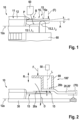
- the Fig.1 shows a side view of an electrical and/or electronic component 10.
- This has an external contact connection 15, which is designed as a connection lug connected on one side.
- the connection is made to a component base body 11, via which the connection lug 15 is contacted with an electrical functional area of the component 10.
- the connection lug 15 is formed, for example, from a sheet metal material, for example from a copper sheet.
- the connection lug 15 has in present embodiment has a bending point B and thus divides the longitudinal extent of the connection lug 15 into at least one longitudinal section I1 of a connection leg 15.1 and an adjoining longitudinal section I2 of a bending leg 15.2.
- connection leg 15.1 is thus connected at one end to the component base body 11 and opens via the other end from the bending point B into one end of the bending leg 15.2.
- the other end of the bending leg 15.2 is exposed.
- the bending leg 15.2 is bent by a compensation angle ⁇ from a connection plane A, in which, for example, a uniform surface side of the still unbent connection lug 15 was arranged before the bend.
- the bending takes place towards a connection side 16 of the connection lug 15.
- the connection side 16 is later used to electrically connect the connection lug 15 as an external connection contact to a contacting partner by means of a connection contact.
- the bending leg 15.2 comprises a connecting surface 16a via which the connecting contact can then be formed.
- the connecting leg 15.1 is preferably arranged with its one surface side in the connection plane A.
- the electrical and/or electronic component 10 also preferably has a housing 12, in particular made of plastic.
- the housing 12 is then formed, for example, from a molding material.
- the electrical and/or electronic component 10 also has a lower connection or support side 12a via which the component 10 can be arranged on a carrier substrate 30.
- the connection lug 15 protrudes from the housing 12 in the area of the connecting leg 15.1 at an exit point P.
- the exit point P is located in particular in the connection plane A, so that the exit point P and the connection plane are arranged at a parallel distance from the lower connection or support side 12a.
- the connection lug 15 is modeled as a bending beam clamped on one side.
- connection side 16a When a force F is applied from the connection side 16a, for example on the exposed end of the bending leg 15.2, a preferably fully elastic or at least partially elastic bending takes place in the direction of the underside connection or support side 12a of the component 10.
- a positional orientation of the connection surface 16a also changes at least against the compensation angle ⁇ .
- the longitudinal section I1 of the connection leg 15.1 is designed to be many times shorter than the longitudinal section I2 of the bending leg 15.2, in particular 2 to 20 times shorter, preferably 5 to 10 times shorter. This results in an increasing rotational movement around the bending point B when the force is applied, which then becomes an essentially rigid swivel joint.
- the bending point B is introduced into a still unbent connecting lug 15 by a bending tool 60, for example.
- the tool 60 comprises, for example, a fixed stop and a movable bending pin, whereby the bending pin bends the connecting lug 15 against the fixed stop in the bending point B towards the connection side 16 by means of a force movement in contact with the latter.
- connection lug In the side view of the Fig.1 only one connection lug is visible in the described embodiment.
- the electrical and/or electronic component 10 can comprise further identical or similar connection lugs 15 exclusively or in addition to at least one external connection contact of a different design.
- the electrical and/or electronic component 10 is prepared for a connection process.
- the carrier substrate 30 is arranged on a carrier substrate 30 via its underside connection or connection side 12a, for example by means of a sintered or solder contact.
- a wide variety of substrate types can be used as the carrier substrate 30, for example a lead frame, a rigid or flexible circuit board, a DBC substrate (double bonded copper), an IMS substrate (insulated metal substrate), an AMB substrate (active metal brazing), an LTCC substrate (low temperature cofired ceramic) or others.
- An initial arrangement 100' is then formed. In this case, a flat area of a support side 20a of a contact partner 20 to be connected is brought into initial contact with the free end of the bending leg 15.2.
- the contact partner 20 can be arranged, for example, by means of an assembly process coming from the connection side 16 of the connection lug 15 in a position in which the support side 20a of the contact point touches the end of the bending leg at an initial contact point E. In this position, the contact partner 20 is held stationary at an end of the contact partner 20 spaced apart from the initial contact point E, for example by a holding tool 70 or by a material or form-fitting and/or force-fitting connection, for example with the Carrier substrate 30.
- a welding mask 80 is placed on a welding side 20b of the contact partner 20 opposite the support side 20a.
- An initial contact can also be formed after the welding mask 80 has been placed on the welding side 20b of a contact partner 20 held stationary on one side and this is moved in the direction of the connection side 16 of the connection lug 15 until the initial contact point E is reached.
- the output arrangement 100' is subjected to a force by a further, for example linear, relative movement R of the welding mask 20 in the direction of the connection side 16 of the connection lug 15. Due to the acting depression force F, the connection lug 15 gives way elastically or at least partially elastically in the direction of the carrier substrate 20 by an at least partial rotational movement D, which also results in a changed position orientation of the connection surface 16a at least opposite to the compensation angle ⁇ of the bending leg 15.2.
- the relative movement R of the welding mask 80 is only held in a welding position in which the connection surface 16a of the connection lug 15 and the support side 20a of the contact partner 20 lie flat against one another.
- a welding contact 40 is then formed as a connection contact using a welding process while maintaining the welding position.
- the welding process is carried out, for example, by means of a laser 50, the laser radiation L of which is directed onto the welding side 20b of the contact partner 20.
- the welding mask 80 is preferably designed in a tube-like manner and in particular has a wall height by which metallic ejections during laser welding are prevented from scattering outside the welding mask 80.
- the formed contact arrangement 100 with the then gap-free welding contact 40 between the connection lug 15 and the contact partner 20 is shown in a side view after removal of the welding mask 80.
- the contact partner 20 is then, for example, a connection clip 20 ⁇ , which is designed in particular as a stamped sheet metal part, preferably made of copper.
- the end of the connecting clip 20' spaced from the welding contact 40 is indirectly connected via a frame element 90 in a force-fitting and/or form-fitting manner to the Carrier substrate 30 and thus held in place, for example via a hole-pin connection.
- a further welding contact 40 is formed as a connecting contact between the connection clip 20' and a connection point 36 of an electronic circuit 35 arranged on the carrier substrate 30.
- the further connecting contact 40 can be formed before, after or together with the connecting contact between the connection clip 20' and the connection lug 15 by means of the laser 50.
- Fig.4 is the contact arrangement from the Fig.3 shown in a perspective view, for example as a circuit part of an inverter 110.
- the electronic circuit 35 comprises a B2 or a B6 bridge, which is formed by at least one described electrical and/or electronic component 10, in particular as a power module, preferably in the form of a mold module.
- two power contacts 15 arranged on the same side are each connected to a connecting clip 20' by means of a gap-free welding contact 40 to form the contact arrangement 100.
Landscapes
- Engineering & Computer Science (AREA)
- Physics & Mathematics (AREA)
- Optics & Photonics (AREA)
- Mechanical Engineering (AREA)
- Plasma & Fusion (AREA)
- Manufacturing & Machinery (AREA)
- Coupling Device And Connection With Printed Circuit (AREA)
- Microelectronics & Electronic Packaging (AREA)
- Structures For Mounting Electric Components On Printed Circuit Boards (AREA)
Description
- Die Erfindung betrifft ein elektrisches und/oder elektronisches Bauelement, eine Kontaktanordnung umfassend das elektrische und/oder elektronische Bauelement sowie ein Verfahren zur Ausbildung der Kontaktanordnung gemäß dem Oberbegriff der unabhängigen Ansprüche.
- Es ist allgemein bekannt eine mechanische und elektrische Verbindung von metallischen Werkstücken mittels Schweißen, beispielsweise mittels eines Laserschweißens, herzustellen. Dies kommt u.a. zum Einsatz beispielsweise beim Verschweißen von Leistungskontakten von Leistungsmodulen innerhalb von elektronischen Leistungsschaltungen. Dabei müssen die beiden Schweißpartner - beispielsweise der Leistungskontakt und ein Anschlusspunkt der elektronischen Schaltung - sehr nahe zusammengebracht werden, in der Regel unterhalb von 100µm Spaltbreite. Bei größeren Spaltabständen kann es ansonsten zu metallischen Auswürfen beim Laserschweißen bis hin zu nicht geschweißten Kontakten kommen. Hinzukommt, dass gerade nicht oder schlecht geschweißte Kontakt optisch kaum zu erkennen sind und diese somit eine Fehlerquelle für Fehlfunktionen darstellen können. Ein idealer Nullspalt zwischen den Schweißpartnern kann technisch einfach erreicht werden, indem beide Schweißpartner mittels einer zangenartigen Vorrichtung unter elastischer und/oder plastischer Verformung bis auf einen spaltfreien Anlagenkontakt zusammengedrückt werden. Gerade bei sehr kompakten elektronischen Schaltungen ist ein erforderlicher Platz für eine derartige Vorrichtung nicht immer vorhanden. Ferner ist die Handhabung einer solchen Vorrichtung oft schwierig, da ein Zugang von beiden Seiten der Schweißpartner erfolgen muss. Zusätzlich ist in der Regel ein Gegenlager für die Schweißvorrichtung erforderlich, wofür eine Auflagefläche - beispielsweise auf dem Trägersubstrat der elektronischen Schaltung - bereitgestellt werden muss.
-
DE102007006601 offenbart die elektrische und mechanische Verbindung einer Kontaktanordnung mittels eines Laserstrahls. - Der Erfindung liegt die Aufgabe zu Grunde, Schweißkontakte von elektrischen und/oder elektronischen Bauelementen innerhalb von kompakten Schaltungen möglichst spaltfrei auszubilden.
- Diese Aufgabe wird durch ein elektrisches und/oder elektronisches Bauelement, eine Kontaktanordnung umfassend das elektrische und/oder elektronische Bauelement sowie ein Verfahren zur Ausbildung der Kontaktanordnung gemäß den unabhängigen Ansprüchen gelöst.
- Ausgegangen wird von einem elektrischen und/oder elektronischen Bauelement mit zumindest einem elektrischen Außenanschlusskontakt. Dieser ist als eine einseitig angebundene Anschlussfahne zur elektrischen Kontaktierung mit einem Kontaktierungspartner ausgebildet. Die Anschlussfahne weist dabei für die elektrische Kontaktierung eine Verbindungsseite mit einer ebenen Verbindungsfläche auf. Sie entspricht daher im mechanischen Modellbild einem einseitig eingespannten Biegebalken. Bevorzugt ist die Anschlussfahne aus einem Blechmaterial, insbesondere als Stanzblech oder Laserblech, ausgebildet, beispielsweise aus Kupfer, und kontaktiert einen elektrischen Funktionsbereich des Bauelementes. Als ein von extern kontaktierter Außenanschlusskontakt ermöglicht dieser das Einbinden des elektrischen Funktionsbereiches beispielsweise innerhalb einer elektronischen Schaltung. Das freiliegende Ende der Anschlussfahne weist einen Biegeschenkel auf, welcher zur Verbindungsseite hin um einen Kompensationswinkel aus der Ebene gebogen ist. Der Biegeschenkel weist dabei die Verbindungsfläche auf. Ferner ist die Anschlussfahne derart nachgiebig ausgebildet, dass bei einem von der Verbindungsseite her Kraft beaufschlagten Anlagenkontakt eines zumindest in diesem Bereich ebenen Kontaktierungspartners auf das freie Ende des Biegeschenkels eine Lageorientierung der Verbindungsfläche zumindest entgegen des Kompensationswinkels bis zu einer spaltfreien Anlage der Verbindungsfläche an den ebenen Kontaktierungspartner anpassbar ist. Somit ist die Anschlussfahne in Hinblick auf einen auszubildenden Schweißkontakt vorteilhaft vorausgehend als optimierter Schweißpartner präpariert. Denn durch die Orientierung des Biegeschenkels auf der Verbindungsseite entgegen einer von dieser Seite einwirkenden Kraftbeaufschlagung, beispielsweise mittels einer zumindest mittelbbar aufliegenden Schweißmaske, ist ein Erstanlagekontakt eines von der Verbindungsseite auf die Anschlussfahne relativ zubewegten ebenen Kontaktierungspartners, beispielsweise ein Verbindungsclip, im Bereich des freien Endes der Anschlussfahne, d.h. des Biegeschenkels ermöglicht. Hierbei kann bei dem Erstanlagenkontakt zwischen der Anschlussfahne und dem Kontaktierungspartner zuerst ein Spalt ausgebildet sein, welcher keilförmig bis zum Erstanlagekontaktpunkt zuläuft. Dieser Spalt lässt sich nun bis zu einer spaltfreien Anlage reduzieren, indem eine erzwungene Verbiegung der Anschlussfahne mittels einer weiteren Kraftbeaufschlagung erwirkt wird, beispielsweise durch eine weitere Relativbewegung der genannten Schweißmaske, bevorzugt einer geradlinigen Relativbewegung. Durch die fortlaufende Verbiegung der Anschlussfahne dreht sich die Flächenlage der Verbindungsfläche entgegen des Kompensationswinkels zur Ebene des Kontaktierungspartners hin bis zur ebenflächigen und somit spaltfreien Anlage.
- Dies entspricht dann einer optimalen Schweißlage, in welcher mittels eines Schweißprozesses ein spaltfreier Schweißkontakt ausbildbar ist. Der vorgesehene Kompensationswinkel ermöglicht daher die gesicherte erforderliche Lagekorrektur der Verbindungsfläche und kompensiert Fehlstellungen, beispielsweise durch Montage- und/oder Fertigungstoleranzen. Da nur eine einseitige Kraftbeaufschlagung von der Verbindungsseite her erforderlich ist, ist die Ausbildung eines Schweißkontaktes innerhalb einer sehr beengten elektronischen Schaltung ohne ein ansonsten erforderliches Gegenlager ermöglicht.
- Durch die in den abhängigen Ansprüchen aufgeführten Maßnahmen sind vorteilhafte Weiterbildungen und Verbesserungen der erfindungsgemäßen elektronischen Baugruppe möglich.
- In einer vorteilhaften Ausführungsform des elektrischen und/oder elektronischen Bauelementes weist der Kompensationswinkel einen Wert in einem Bereich von 0,5° bis 5° auf, bevorzugt in einem Bereich von 0,5° bis 1,5°. Es hat sich gezeigt, dass in diesem Bereich bereits viele toleranzbehaftete Ausgangsfehlstellungen durch die ermöglichte Lagekorrektur der Verbindungsfläche kompensiert werden können und die Fertigungszeiten zur Ausbildung eines Spalts freien Schweißkontaktes aufgrund von dann kurz gehaltenen Wegen bis zur Erreichung der optimalen Schweißlage klein gehalten werden können. Bevorzugt erfolgt die Erreichung der optimalen Schweißlage durch eine vollelastische Nachgiebigkeit der Anschlussfahne, zumindest jedoch alternativ bevorzugt durch eine teilelastische Nachgiebigkeit der Anschlussfahne. Auf diese Weise können auch die Beaufschlagungskräfte für die Lagekorrektur der Verbindungsfläche klein gehalten werden, so dass Beschädigungen während der Ausbildung eines Schweißkontaktes auszuschließen sind.
- In einer vorteilhaften Weiterbildung des elektrischen und/oder elektronischen Bauelementes weist die Anschlussfahne einen Anschlussschenkel auf. Dieser mündet mit seinem einen Ende über einen Biegebereich in den Biegeschenkel und umfasst an seinem anderen Ende dann die einseitige Anbindung der Anschlussfahne innerhalb des elektrischen und/oder elektronischen Bauelementes. Vorteilhaft weist die Anschlussfahne nur eine Biegestelle auf, so dass die Präparierung der Anschlussfahne sich für einen optimal auszubildenden Schweißkontakt sehr kostengünstig umsetzen lässt. Hierbei kann die Biegung vorzugsweise in eine ursprüngliche Anschlussfahne aus einem ebenen Blechmaterial eingebracht sein, so dass insbesondere ein sich geradlinig erstreckender Anschlussschenkel verbleibt. Allgemein vorteilhaft ist eine Längserstreckung des Anschlussschenkels um ein Vielfaches kürzer als eine Längserstreckung des Biegeschenkels, insbesondere um das 2 bis 20-fache kürzer, bevorzugt um das 5 bis 10-fache kürzer. Auf diese Weise ergibt sich zunehmend eine Nachgiebigkeit der Anschlussfahne mehr oder weniger allein durch den Biegeschenkel. Dabei stellt die Biegestelle dann angenähert die Funktion eines starren Drehgelenks. Ferner lässt sich die optimale Schweißposition genauer einstellen.
- In einer bevorzugten Ausführungsform des elektrischen und/oder elektronischen Bauelements weist dieses ein festes Gehäuse auf, aus welchem die Anschlussfahne einseitig angebunden hervorsteht. Das Gehäuse ist bevorzugt aus einem Kunststoff, insbesondere einem Moldmaterial, gebildet. Dabei ist weiter bevorzugt die Anschlussfahne an ihrem angebundenen Ende von dem Kunststoff allseitig umschlossen bzw. umhüllt. Mittels des Gehäuses können dann vorteilhaft erhöhte Beaufschlagungskräfte auf die Anschlussfahne schadensfrei von dem elektrischen und/oder elektronischen Bauelement aufgenommen werden.
- Weitere Vorteile zeigen sich in einer Ausführungsform des elektrischen und/oder elektronischen Bauelementes, welches eine beispielsweise unterseitige Anschluss- und/oder Auflageseite zu einem Trägersubstrat aufweist. Dabei ist die Anschlussfahne zur unterseitigen Anschluss- und/oder Auflageseite hin beabstandet angeordnet. Ferner ist in einer Draufsicht auf die Anschluss- oder Auflageseite die Anschlussfahne zu dieser seitlich abstehend innerhalb des elektrischen und/oder elektronischen Bauelements einseitig angebunden. Der Biegeschenkel zeigt dabei von der Anschluss- und/oder Auflageseite weg. Damit ist insgesamt ein freier Zugang zu den Anschlussfahnen für eine einseitige Kraftbeaufschlagung von der Verbindungsseite her gegeben. Außerdem ist durch die Beabstandung eine ungehinderte Verbiegung der Anschlussfahne in Richtung der Anschluss- oder Auflageseite ermöglicht. Bevorzugt weist ein gehäustes elektrisches und/oder elektronisches Bauelement eine Austrittsstelle eines Anschlussschenkels der Anschlussfahne aus dem Gehäuse in einer zur Anschluss- oder Auflageseite parallelen Anschlussebene auf. Weiter bevorzugt liegt der Anschlussschenkel bis zur Biegestelle innerhalb dieser Anschlussebene, wogegen der Biegeschenkel insbesondere senkrecht zu einer Längserstreckung des Anschlussschenkels aus der Anschlussebene in Richtung der Verbindungsseite der Anschlussfahne gebogen ist.
- Allgemein bevorzugt ist das elektrische und/oder elektronische Bauelement als ein Leistungsmodul ausgebildet, insbesondere in Form eines Moldmodules.
- Dabei ist die Anschlussfahne als Leistungskontakt ausgebildet. Das elektrische und/oder elektronische Bauelement kann insgesamt auch zwei, drei oder noch mehr derartige Anschlussfahnen ausschließlich oder neben zumindest einem andersartig ausgebildeten Außenanschlusskontakt aufweisen.
- Die Erfindung führt auch zu einer Kontaktanordnung, umfassend zumindest ein elektrisches und/oder elektronisches Bauelement in zumindest einer der zuvor beschriebenen Ausführungsformen, wobei zwischen der Anschlussfahne im Bereich der Verbindungsfläche und einem - zumindest in dem ausgebildeten Verbindungsbereich - ebenen Kontaktierungspartner ein insbesondere spaltfreier Verbindungskontakt ausgebildet ist. Ein solcher Verbindungskontakt stellt eine über Lebensdauer funktionssichere Verbindung beispielsweise zu einer elektronischen Schaltung dar. Der Verbindungskontakt ist dabei insbesondere als ein Schweißkontakt ausgebildet. Bei der Anwendung eines Laserprozesses ergibt sich dabei insbesondere ein Laserschweißkontakt.
- In einer bevorzugten Ausführungsform der Kontaktanordnung ist diese als Teil einer elektronischen Schaltung auf einem Trägersubstrat ausgebildet. Der Kontaktierungspartner ist insbesondere ein Verbindungsclip, welcher die Anschlussfahne und einen Anschlusspunkt der elektronischen Schaltung überbrückend miteinander verbindet. Der Verbindungsclip ist dabei beispielweise ein Stanzblechteil, insbesondere aus Kupfer. Neben ebenen Flächen in den Verbindungsbereichen zur Anschlussfahne bzw. zum Anschlusspunkt kann der Verbindungsclip ein oder mehrere Biegungen aufweisen, beispielsweise um einen anwendungsbedingten Höhenversatz zwischen der Anschlussfahne und dem Verbindungspunkt der elektronischen Schaltung zu überspannen. Ferner kann der Verbindungsclip Aussparungen, insbesondere in Form von Längsschlitzen zwischen den Verbindungsstellen, aufweisen. Auf diese Weise erhält der Verbindungsclip eine ausreichende mechanische Elastizität, um eine Ausrichtung der vorgesehenen Fügeflächen in den Verbindungsbereichen durch ein Verbiegen und/oder Tordieren bis zu einer spaltfreien Anlage zum jeweiligen Schweißpartner zu ermöglichen.
- Bevorzugt ist die elektronische Schaltung als B2- oder B6-Brücke ausgebildet, insbesondere als Schaltungsteil eines Inverters.
- Die Erfindung führt auch zu einem Verfahren zur Ausbildung einer Kontaktanordnung nach zumindest einer der zuvor beschriebenen Ausführungsformen, mit den nachfolgenden Verfahrensschritten:
- a) Bereitstellen eines elektrischen und/oder elektronischen Bauelementes nach zumindest einer der zuvor beschriebenen Ausführungsformen, beispielsweise indem dieses über seine beispielsweise unterseitige Anschluss- und/oder Auflageseite auf einem Trägersubstrat angeordnet wird,
- b) Ausbildung einer Ausgangsanordnung, indem eine ebene Auflageseite eines Kontaktierungspartners von der Verbindungsseite der Anschlussfahne her in Anlagenkontakt mit dem freiliegenden Ende des Biegeschenkels angeordnet wird und eine Schweißmaske auf einer der Auflageseite des Kontaktierungspartners gegenüberliegenden Schweißseite aufgelegt wird,
- c) Kraftbeaufschlagung der Ausgangsanordnung durch eine Niederdrückkraft, insbesondere mittels einer bevorzugt geradlinigen Relativbewegung der Schweißmaske, derart, dass durch ein Nachgeben der Anschlussfahne in Kraftrichtung eine geänderte Lageorientierung der Verbindungsfläche zumindest entgegen des Kompensationswinkels des Biegeschenkels erfolgt,
- d) Festhalten einer Schweißposition, bei welcher die Verbindungsfläche der Anschlussfahne und die Auflageseite des Kontaktierungspartners ebenflächig aneinander liegen,
- e) Ausbildung eines Schweißkontaktes, beispielsweise mittels Lasern auf der Schweißseite des Kontaktierungspartners, als spaltfreier Verbindungskontakt zwischen der Anschlussfahne und dem Kontaktierungspartner.
- Bei einer vorteilhaften Ausführungsform des Verfahrens ist der Kontaktierungspartner als Verbindungsclip ausgebildet, wobei vor oder während des Verfahrensschrittes b) ein zum Anlagenkontakt beabstandetes Ende des Verbindungsclips ortsfest gehalten wird. Dies kann beispielsweise mittels eines Haltewerkzeugs erfolgen, welches das besagte Ende aufnimmt und ortsfest fixiert. Alternativ erfolgt eine ortsfeste Fixierung durch eine zumindest mittelbare stoff- oder kraft- und/oder formschlüssigen Verbindung mit dem Trägersubstrat. Durch das einseitige Fixieren können sich die Anschlussfahne und der Verbindungsclip allein durch die Kraftbeaufschlagung und Verbiegung bis zu einer spaltfreien Anlage im Verbindungsbereich zueinander ausrichten.
- In einer vorteilhaften Weiterbildung des Verfahrens wird zwischen dem ortsfest gehaltenen Ende des Verbindungsclips und dem auszubildenden bzw. ausgebildeten Verbindungskontakt mit der Anschlussfahne ein weiterer Verbindungskontakt zwischen dem Verbindungsclip und einem Anschlusspunkt einer elektronischen Schaltung ausgebildet, insbesondere als Schweißkontakt. Die Ausbildung des weiteren Verbindungskontakts erfolgt dabei zeitlich vor, nach oder zusammen mit dem Verbindungskontakt zwischen dem Verbindungsclip und der Anschlussfahne.
- Weitere Vorteile, Merkmale und Einzelheiten der Erfindung ergeben sich aus der nachfolgenden Beschreibung bevorzugter Ausführungsbeispiele sowie anhand der Zeichnung. Diese zeigt in:
- Fig. 1:
- ein elektrisches und/oder elektronisches Bauelement mit einem endseitigen Biegeschenkel innerhalb einer einseitig angebundenen Anschlussfahne als Außenkontaktanschluss in einer Seitenansicht,
- Fig. 2:
- eine Ausgangsanordnung umfassend ein elektrisches und/oder elektronisches Bauelement aus
Fig. 1 in einer Erstkontaktanlage mit einem Kontaktierungspartner mit einem Erstkontaktanlagepunkt am freiliegenden Ende des Biegeschenkels der Anschlussfahne in einer Seitenansicht, - Fig. 3:
- eine aus der Ausgangsanordnung nach
Fig. 2 hervorgegangene Kontaktanordnung nach einer Kraftbeaufschlagung und Verschweißung unter Ausbildung eines Spalts freien Schweißkontaktes zwischen der Anschlussfahne und dem Kontaktierungspartner in einer Seitenansicht, - Fig. 4:
- eine Kontaktanordnung innerhalb einer elektronischen Schaltung, insbesondere einer Inverterschaltung, in einer perspektivischen Darstellung.
- In den Figuren sind funktional gleiche Bauelemente jeweils mit gleichen Bezugszeichen gekennzeichnet.
- Die
Fig. 1 zeigt in einer Seitenansicht ein elektrisches und/oder elektronisches Bauelements 10. Dieses weist einen Außenkontaktanschluss 15 auf, welcher als eine einseitig angebundene Anschlussfahne ausgebildet ist. Die Anbindung erfolgt an eine Bauelementgrundkörper 11, über welchen die Anschlussfahne 15 mit einem elektrischen Funktionsbereich des Bauelementes 10 kontaktiert ist. Die Anschlussfahne 15 ist beispielhaft aus einem Blechmaterial gebildet, beispielsweise aus einem Kupferblech. Die Anschlussfahne 15 weist im vorliegenden Ausführungsbeispiel eine Biegestelle B auf und unterteilt damit über die Längserstreckung der Anschlussfahne 15 diese abschnittsweise zumindest in einen Längsabschnitt I1 eines Anschlussschenkels 15.1 und in einen anschließenden Längsabschnitt I2 eines Biegeschenkels 15.2. Der Anschlussschenkel 15.1 ist damit mit seinem einen Ende einseitig an den Bauelementgrundkörper 11 angebunden und mündet über das andere Ende ab der Biegestelle B in das eine Ende des Biegeschenkels 15.2. Das andere Ende des Biegeschenkels 15.2 ist freiliegend. Der Biegeschenkel 15.2 ist dabei um einen Kompensationswinkel α aus einer Anschlusseben A gebogen, in welcher beispielsweise vor der Biegung eine einheitliche Oberflächenseite der noch ungebogenen Anschlussfahne 15 angeordnet war. Die Biegung erfolgt dabei zu einer Verbindungsseite 16 der Anschlussfahne 15 hin. Über die Verbindungsseite 16 erfolgt später mittels eines Verbindungskontaktes eine elektrische Verbindung der Anschlussfahne 15 als Außenanschlusskontakt an einen Kontaktierungspartner. Hierzu umfasst der Biegeschenkel 15.2 eine Verbindungsfläche 16a über welche der Verbindungskontakt dann ausbildbar ist. Bevorzugt ist der Anschlussschenkel 15.1 mit seiner einen Oberflächenseite in der Anschlussebene A angeordnet. Weiter bevorzugt weist das elektrische und/oder elektronische Bauelement 10 ein Gehäuse 12 auf, insbesondere aus Kunststoff. Das Gehäuse 12 ist dann beispielsweise aus einem Moldmaterial gebildet. Dabei weist das elektrische und/oder elektronische Bauelement 10 auch eine unterseitige Anschluss- oder Auflageseite 12a auf, über welche das Bauelement 10 auf einem Trägersubstrat 30 angeordnet werden kann. Die Anschlussfahne 15 tritt dabei im Bereich des Anschlussschenkels 15.1 in einem Austrittspunkt P aus dem Gehäuse 12 hervor. Der Austrittspunkt P befindet sich insbesondere in der Anschlussebene A, so dass der Austrittspunkt P und die Anschlussebene in einer parallelen Beabstandung zur unterseitigen Anschluss- oder Auflageseite 12a angeordnet sind. Insgesamt zeigt sich die Anschlussfahne 15 modellhaft als ein einseitig eingespannter Biegebalken. Bei einer Krafteinwirkung mit einer Kraft F von der Verbindungsseite 16a her, beispielsweise auf das freiliegende Ende des Biegeschenkels 15.2, erfolgt eine bevorzugt vollelastische oder zumindest teilelastische Verbiegung in Richtung der unterseitigen Anschluss- oder Auflageseite 12a des Bauelementes 10. Hierbei ändert sich auch eine Lageorientierung der Verbindungsfläche 16a zumindest entgegen des Kompensationswinkels α. Bevorzugt ist dabei der Längsabschnitt I1 des Anschlussschenkels 15.1 um ein Vielfaches kürzer ausgebildet als der Längsabschnitt I2 des Biegeschenkels 15.2, insbesondere um das 2 bis 20-fache kürzer, bevorzugt um das 5 bis 10-fache kürzer. Hierdurch ergibt sich bei der Krafteinwirkung zunehmend eine Drehbewegung um die Biegestelle B als dann im Wesentlichen starres Drehgelenk. Die Biegestelle B wird beispielsweise durch ein Biegewerkzeug 60 in eine noch ungebogene Anschlussfahne 15 eingebracht. Das Werkzeug 60 umfasst dabei beispielsweise einen festen Anschlag und einen verfahrbaren Biegestift, wobei der Biegestift durch eine Kraftbewegung in Kontakt mit der Anschlussfahne 15 diese gegen den festen Anschlag in der Biegestelle B zur Verbindungsseite 16 hin verbiegt. - In der Seitenansicht der
Fig. 1 ist nur eine Anschlussfahne in der beschriebenen Ausführung sichtbar. Grundsätzlich kann das elektrische und/oder elektronische Bauelement 10 noch weitere gleiche oder gleichartige Anschlussfahnen 15 ausschließlich oder neben zumindest einem anders ausgeführten Außenanschlusskontakt umfassen. - Zur Ausbildung einer Kontaktanordnung 100 umfassend das elektrische und/oder elektronische Bauelement 10 mit einem Verbindungskontakt 40 zu einem Kontaktierungspartner 20 kann - wie nachfolgend mit Hilfe der
Fig. 2 und3 beschrieben - verfahren werden. Zuerst wird das elektrische und/oder elektronische Bauelement 10 für einen Verbindungsprozess bereitgestellt. Hierfür wird es beispielsweise über seine unterseitige Anschluss- oder Verbindungsseite 12a auf einem Trägersubstrat 30 angeordnet, beispielsweise mittels eines Sinter- oder Lotkontakts. Als Trägersubstrat 30 können unterschiedlichste Substrattypen genutzt werden, beispielsweise ein Leadframe, eine starre oder flexible Leiterplatte, ein DBC-Substrat (double bonded copper), ein IMS-Substrat (insulated metal substrat), ein AMB-Substrat (active metal brazing) ein LTCC-Substrat (low temperature cofired ceramic) oder andere. Nachfolgend wird eine Ausgangsanordnung 100' ausgebildet. Dabei wird ein ebener Bereich einer Auflageseite 20a eines zu verbindenden Kontaktierungspartners 20 in einen Erstanlagekontakt mit dem freien Ende des Biegeschenkels 15.2 gebracht. - Der Kontaktierungspartner 20 kann beispielsweise durch einen Bestückprozess von der Verbindungsseite 16 der Anschlussfahne 15 her kommend in einer Position angeordnet werden, in welcher die Auflageseite 20a des Kontaktierungspunktes das Ende des Biegeschenkels in einem Erstanlagepunkt E berührt. In dieser Position wird der Kontaktierungspartner 20 an einem zum Erstanlagepunkt E beabstandenden Ende des Kontaktierungspartners 20 ortsfest gehalten, beispielsweise durch ein Haltewerkzeug 70 oder durch eine stoff- oder form- und/oder kraftschlüssige Verbindung, beispielsweise mit dem Trägersubstrat 30. Zeitgleich mit dem Bestückprozess oder alternativ anschließend wird eine Schweißmaske 80 auf eine der Auflageseite 20a gegenüberliegende Schweißseite 20b des Kontaktierungspartners 20 aufgelegt. Ebenso kann ein Erstanlagekontakt ausgebildet werden, nachdem zuvor auf die Schweißseite 20b eines einseitig ortsfest gehaltenen Kontaktierungspartners 20 die Schweißmaske 80 aufgelegt wurde und diese in Richtung der Verbindungsseite 16 der Anschlussfahne 15 bis zum Erreichen der Erstanlagepunktes E verfahren wird.
- Grundsätzlich wird nach Vorliegen eines Erstanlagepunktes E durch eine weitere beispielsweise geradlinige Relativbewegung R der Schweißmaske 20 in Richtung der Verbindungsseite 16 der Anschlussfahne 15 die Ausgangsanordnung 100' kraftbeaufschlagt. Durch die einwirkende Niederdrückkraft F gibt die Anschlussfahne 15 in Richtung Trägersubstrat 20 elastisch oder zumindest teilelastisch durch eine zumindest anteilige Drehbewegung D nach, wodurch auch eine geänderte Lageorientierung der Verbindungsfläche 16a zumindest entgegen des Kompensationswinkels α des Biegeschenkels 15.2 erfolgt. Die Relativbewegung R der Schweißmaske 80 wird erst in einer Schweißposition festgehalten, bei welcher die Verbindungsfläche 16a der Anschlussfahne 15 und die Auflageseite 20a des Kontaktierungspartners 20 ebenflächig aneinander liegen. Daraufhin wird mit Hilfe eines Schweißprozesses unter Beibehaltung der Schweißposition ein Schweißkontakt 40 als Verbindungskontakt ausgebildet. Der Schweißprozess erfolgt beispielsweise mittels eines Lasers 50, dessen Laserstrahlung L auf die Schweißseite 20b des Kontaktierungspartners 20 gerichtet ist. Die Schweißmaske 80 ist bevorzugt rohrartig gestaltet und weist dabei insbesondere eine Wandungshöhe auf, durch welche metallischen Auswürfen beim Laserschweißen an einer Streuung außerhalb der Schweißmaske 80 gehindert werden.
- In der
Fig. 3 ist die ausgebildete Kontaktanordnung 100 mit dem dann spaltfreien Schweißkontakt 40 zwischen der Anschlussfahne 15 und dem Kontaktierungspartner 20 in einer Seitenansicht nach dem Entfernen der Schweißmaske 80 gezeigt. Der Kontaktierungspartner 20 ist dann beispielsweise ein Verbindungsclips 20`, welcher insbesondere als ein Stanzblechteil ausgebildet, bevorzugt aus Kupfer. Im Gegensatz zur Darstellung in derFig. 2 ist das dem Schweißkontakt 40 beabstandete Ende des Verbindungsclips 20' mittelbar über ein Rahmenelement 90 kraft- und/oder formschlüssig mit dem Trägersubstrat 30 verbunden und somit ortsfest gehalten, beispielsweise über eine Loch-Stiftverbindung. Zusätzlich ist zwischen dem ortsfest gehaltenen Ende des Verbindungsclips 20' und dem ausgebildeten Schweißkontakt 40 mit der Anschlussfahne15 ein weiterer Schweißkontakt 40 als Verbindungskontakt zwischen dem Verbindungsclip 20' und einem Anschlusspunkt 36 einer auf dem Trägersubstrat 30 angeordneten elektronischen Schaltung 35 ausgebildet ist. Der weitere Verbindungskontakt 40 kann dabei zeitlich vor, nach oder zusammen mit dem Verbindungskontakt zwischen dem Verbindungsclip 20' und der Anschlussfahne 15 mittels dem Laser 50 ausgebildet werden. - In der
Fig. 4 ist die Kontaktanordnung aus derFig. 3 in einer perspektivischen Darstellung beispielsweise als Schaltungsteil eines Inverters 110 gezeigt. Die elektronische Schaltung 35 umfasst hierbei eine B2- oder eine B6-Brücke, welche durch zumindest ein beschriebenes elektrisches und/oder elektronisches Bauteil 10 gebildet ist, insbesondere als ein Leistungsmodul, bevorzugt in Form eines Moldmodules. Im vorliegenden Ausführungsbeispiel sind zwei auf der gleichen Seite angeordnete Leistungskontakte 15 unter Ausbildung der Kontaktanordnung 100 jeweils mit einem Verbindungsclip 20' mittels eines Spalts freien Schweißkontaktes 40 verbunden.
Claims (15)
- Elektrisches und/oder elektronisches Bauelement (10) mit zumindest einem elektrischen Außenanschlusskontakt (15), welcher als eine einseitig angebundene Anschlussfahne (15) zur elektrischen Kontaktierung mit einem Kontaktierungspartner (20, 20') ausgebildet ist und die Anschlussfahne (15) für die elektrische Kontaktierung eine Verbindungsseite (16) mit einer ebenen Verbindungsfläche (16a) aufweist, dass das freiliegende Ende der Anschlussfahne (15) einen Biegeschenkel (15.2) aufweist, welcher zur Verbindungsseite (16) hin um einen Kompensationswinkel (α) aus der Ebene (A) gebogen ist, wobei der Biegeschenkel (15.2) die Verbindungsfläche (16a) aufweist und die Anschlussfahne (15) derart nachgiebig ausgebildet ist, dadurch gekennzeichnet, dass bei einem von der Verbindungsseite (16) her Kraft beaufschlagten Anlagenkontakt eines ebenen Kontaktierungspartners (20, 20') auf das freie Ende des Biegeschenkels (15.2) eine Lageorientierung der Verbindungsfläche (16a) entgegen des Kompensationswinkels (α) bis zu einer spaltfreien Anlage der Verbindungsfläche (16a) an den ebenen Kontaktierungspartner (20, 20`) anpassbar ist.
- Elektrisches und/oder elektronisches Bauelement (10) nach Anspruch 1,
dadurch gekennzeichnet, dass
der Kompensationswinkel (α) einen Wert in einem Bereich von 0,5° bis 5° aufweist, bevorzugt in einem Bereich von 0,5° bis 1,5°. - Elektrisches und/oder elektronisches Bauelement (10) nach Anspruch 1 oder 2,
dadurch gekennzeichnet, dass
die Anschlussfahne (15) einen Anschlussschenkel (15.1) aufweist, insbesondere einen sich geradlinig erstreckenden Anschlussschenkel (15.1), welcher mit seinem einen Ende über eine Biegestelle (B) in den Biegeschenkel (15.2) mündet und an seinem anderen Ende eine einseitige Anbindung der Anschlussfahne (15) innerhalb des elektrischen und/oder elektronischen Bauelementes (10) umfasst. - Elektrisches und/oder elektronisches Bauelement (10) nach Anspruch 3,
dadurch gekennzeichnet, dass
eine Längserstreckung des Anschlussschenkels (15.1) um ein Vielfaches kürzer ist als eine Längserstreckung des Biegeschenkels (15,2), insbesondere um das 2 bis 20-fache kürzer, bevorzugt um das 5 bis 10-fache kürzer. - Elektrisches und/oder elektronisches Bauelementnach (10) nach einem der vorhergehenden Ansprüche,
dadurch gekennzeichnet, dass
das elektrische und/oder elektronische Bauelement (10) ein Gehäuse (12) aufweist, aus welchem die Anschlussfahne (15) einseitig angebunden hervorsteht. - Elektrisches und/oder elektronisches Bauelement (10) nach einem der vorhergehenden Ansprüche,
dadurch gekennzeichnet, dass
das elektrische und/oder elektronische Bauelement (10) eine Anschluss- und/oder Auflageseite (12a) zu einem Trägersubstrat (30) aufweist, wobei die Anschlussfahne (15) zur Anschluss- und/oder Auflageseite (12a) hin beabstandet angeordnet ist und in einer Draufsicht auf die Anschluss- oder Auflageseite (12a) zu dieser seitlich abstehend innerhalb des elektrischen und/oder elektronischen Bauelements (10) einseitig angebunden ist, wobei der Biegeschenkel (15.2) von der Anschluss- und/oder Auflageseite (12a) wegzeigt. - Elektrisches und/oder elektronisches Bauelement (10) nach einem der vorhergehenden Ansprüche,
dadurch gekennzeichnet, dass
das elektrische und/oder elektronische Bauelement (10) als ein Leistungsmodul ausgebildet ist, insbesondere in Form eines Moldmodules. - Kontaktanordnung (100), umfassend zumindest ein elektrisches und/oder elektronisches Bauelement (10) gemäß einem der vorhergehenden Ansprüche, wobei zwischen der Anschlussfahne (15) im Bereich der Verbindungsfläche (16a) und einem ebenen Kontaktierungspartner (20, 20`) ein insbesondere Spalt freier Verbindungskontakt (40) ausgebildet ist.
- Kontaktanordnung (100) nach Anspruch 8,
dadurch gekennzeichnet, dass
der Verbindungskontakt (40) als ein Schweißkontakt ausgebildet ist, insbesondere als ein Laserschweißkontakt. - Kontaktanordnung (100) nach einem der Ansprüche 8 oder 9,
dadurch gekennzeichnet, dass
die Kontaktanordnung (100) als Teil einer elektronischen Schaltung (35) auf einem Trägersubstrat (30) ausgebildet ist, wobei der Kontaktierungspartner (20, 20') ein Verbindungsclip ist, welcher die Anschlussfahne (15) und einen Anschlusspunkt (36) der elektronischen Schaltung (35) überbrückend miteinander verbindet. - Kontaktanordnung (100) nach Anspruch 10,
dadurch gekennzeichnet, dass
die elektronische Schaltung als B2- oder B6-Brücke (120) ausgebildet ist, insbesondere als Schaltungsteil eines Inverters (110). - Verfahren zur Ausbildung einer Kontaktanordnung (100) nach einem der Ansprüche 8 bis 11, mit den nachfolgenden Verfahrensschritten:a) Bereitstellen eines elektrischen und/oder elektronischen Bauelementes (10) nach einem der Ansprüche 1 bis 7, beispielsweise indem dieses über seine unterseitige Anschluss- und/oder Auflageseite (12a) auf einem Trägersubstrat (30) angeordnet wird,b) Ausbildung einer Ausgangsanordnung (100'), indem eine ebene Auflageseite (20a) eines Kontaktierungspartners (20, 20`) von der Verbindungsseite (16) der Anschlussfahne (15) her in Anlagenkontakt mit dem freiliegenden Ende des Biegeschenkels (15.2) angeordnet wird und eine Schweißmaske (80) auf einer der Auflageseite (20a) des Kontaktierungspartners (20, 20') gegenüberliegenden Schweißseite (20b) aufgelegt wird,c) Kraftbeaufschlagung der Ausgangsanordnung (100') durch eine Niederdrückkraft (F), insbesondere mittels einer bevorzugt geradlinigen Relativbewegung (R) der Schweißmaske (80), derart, dass durch ein Nachgeben der Anschlussfahne (15) in Kraftrichtung eine geänderte Lageorientierung der Verbindungsfläche (16a) entgegen des Kompensationswinkels (α) des Biegeschenkels (15.2) erfolgt,d) Festhalten einer Schweißposition, bei welcher die Verbindungsfläche (16a) der Anschlussfahne (15) und die Auflageseite (20a) des Kontaktierungspartners (20, 20') ebenflächig aneinander liegen,e) Ausbildung eines Schweißkontaktes (40), beispielsweise mittels Lasern auf der Schweißseite (20b) des Kontaktierungspartners (20, 20'), als Spalt freier Verbindungskontakt (40) zwischen der Anschlussfahne (15) und dem Kontaktierungspartner (20, 20').
- Verfahren nach Anspruch 12,
dadurch gekennzeichnet, dass
der Kontaktierungspartner (20) als Verbindungsclip (20') ausgebildet ist, wobei vor oder während des Verfahrensschrittes b) ein zum Anlagenkontakt beabstandetes Ende des Verbindungsclips (20') ortsfest gehalten wird, beispielsweise mittels eines Haltewerkzeugs (70) oder einer zumindest mittelbaren stoff- oder kraft- und/oder formschlüssigen Verbindung mit dem Trägersubstrat (30). - Verfahren nach Anspruch 13,
dadurch gekennzeichnet, dass
zwischen dem ortsfest gehaltenen Ende des Verbindungsclips (20') und dem auszubildenden bzw. ausgebildeten Verbindungskontakt (40) mit der Anschlussfahne (15) ein weiterer Verbindungskontakt (40) zwischen dem Verbindungsclip (20') und einem Anschlusspunkt (36) einer elektronischen Schaltung (35) ausgebildet wird, insbesondere als Schweißkontakt. - Verfahren nach Anspruch 14,
dadurch gekennzeichnet, dass
der weitere Verbindungskontakt (40) zeitlich vor, nach oder zusammen mit dem Verbindungskontakt (40) zwischen dem Verbindungsclip (20, 20`) und der Anschlussfahne (15) ausgebildet wird.
Applications Claiming Priority (2)
| Application Number | Priority Date | Filing Date | Title |
|---|---|---|---|
| DE102019211077.0A DE102019211077A1 (de) | 2019-07-25 | 2019-07-25 | Elektrisches und/oder elektronisches Bauelement und Kontaktanordnung |
| PCT/EP2020/070758 WO2021013915A1 (de) | 2019-07-25 | 2020-07-23 | Elektrisches und/oder elektronisches bauelement und kontaktanordnung |
Publications (2)
| Publication Number | Publication Date |
|---|---|
| EP4004978A1 EP4004978A1 (de) | 2022-06-01 |
| EP4004978B1 true EP4004978B1 (de) | 2024-05-15 |
Family
ID=71899710
Family Applications (1)
| Application Number | Title | Priority Date | Filing Date |
|---|---|---|---|
| EP20750192.5A Active EP4004978B1 (de) | 2019-07-25 | 2020-07-23 | Elektrisches und/oder elektronisches bauelement und kontaktanordnung |
Country Status (5)
| Country | Link |
|---|---|
| US (1) | US20220270956A1 (de) |
| EP (1) | EP4004978B1 (de) |
| CN (1) | CN114175406A (de) |
| DE (1) | DE102019211077A1 (de) |
| WO (1) | WO2021013915A1 (de) |
Cited By (1)
| Publication number | Priority date | Publication date | Assignee | Title |
|---|---|---|---|---|
| DE102024209294A1 (de) | 2024-09-26 | 2026-03-26 | Volkswagen Aktiengesellschaft | Verfahren zur Formkorrektur einer Baugruppe |
Families Citing this family (1)
| Publication number | Priority date | Publication date | Assignee | Title |
|---|---|---|---|---|
| DE102021120682B4 (de) | 2021-08-09 | 2025-07-17 | Audi Aktiengesellschaft | Verfahren zum Herstellen eines Leistungsmoduls für ein Elektrofahrzeug |
Family Cites Families (9)
| Publication number | Priority date | Publication date | Assignee | Title |
|---|---|---|---|---|
| US5240170A (en) * | 1992-06-05 | 1993-08-31 | Matsushita Electric Industrial Co., Ltd. | Method for bonding lead of IC component with electrode |
| US6392778B1 (en) * | 1999-03-17 | 2002-05-21 | Koninklijke Philips Electronics N.V. | Opto-electronic element |
| CN101669254B (zh) * | 2007-01-19 | 2013-03-20 | 莫列斯公司 | 端子组件及连接器 |
| DE102007003792B4 (de) * | 2007-01-19 | 2011-08-25 | WAGO Verwaltungsgesellschaft mbH, 32423 | Blattfederkontakt für eine elektrische Leiteranschlußklemme |
| DE102007006601B4 (de) * | 2007-02-09 | 2008-12-04 | Siemens Ag | Anschluss, Verfahren und Vorrichtung zur gleichmäßigen Einkopplung von Laserstrahlen beim Laserschweißen und Laserlöten, insbesondere an hoch reflektierenden Materialien |
| DE102007012501A1 (de) * | 2007-03-15 | 2008-09-18 | Continental Automotive Gmbh | Anordnung aus einem Leitungsträger und einem Schaltungsträger |
| KR20090110558A (ko) * | 2008-04-18 | 2009-10-22 | (주)우주일렉트로닉스 | 단자부의 상하면이 노출된 가요성 평판 케이블과 이를이용한 커넥터 및 그 제조방법 |
| CN201590512U (zh) * | 2009-11-05 | 2010-09-22 | 番禺得意精密电子工业有限公司 | 电连接器 |
| DE102015109073B4 (de) * | 2015-06-09 | 2023-08-10 | Infineon Technologies Ag | Elektronische Vorrichtungen mit erhöhten Kriechstrecken |
-
2019
- 2019-07-25 DE DE102019211077.0A patent/DE102019211077A1/de not_active Withdrawn
-
2020
- 2020-07-23 US US17/625,151 patent/US20220270956A1/en active Pending
- 2020-07-23 WO PCT/EP2020/070758 patent/WO2021013915A1/de not_active Ceased
- 2020-07-23 EP EP20750192.5A patent/EP4004978B1/de active Active
- 2020-07-23 CN CN202080053575.3A patent/CN114175406A/zh active Pending
Cited By (1)
| Publication number | Priority date | Publication date | Assignee | Title |
|---|---|---|---|---|
| DE102024209294A1 (de) | 2024-09-26 | 2026-03-26 | Volkswagen Aktiengesellschaft | Verfahren zur Formkorrektur einer Baugruppe |
Also Published As
| Publication number | Publication date |
|---|---|
| EP4004978A1 (de) | 2022-06-01 |
| CN114175406A (zh) | 2022-03-11 |
| US20220270956A1 (en) | 2022-08-25 |
| WO2021013915A1 (de) | 2021-01-28 |
| DE102019211077A1 (de) | 2021-01-28 |
Similar Documents
| Publication | Publication Date | Title |
|---|---|---|
| EP0712265A1 (de) | Baugruppe | |
| DE102019125108A1 (de) | Leistungselektronikanordnung umfassend eine Leiterplatte und ein Leistungsmodul, Verfahren zur Herstellung einer Leistungselektronikanordnung, Kraftfahrzeug umfassend eine Leistungselektronikanordnung | |
| EP4004978B1 (de) | Elektrisches und/oder elektronisches bauelement und kontaktanordnung | |
| WO2019219536A1 (de) | Kontaktanordnung, elektronikbaugruppe umfassend die kontaktanordnung und verfahren zur ausbildung der kontaktanordnung | |
| DE102006018902B4 (de) | Elektronisches Schaltungsgerät und Verfahren zur Herstellung desselben | |
| DE19912834B4 (de) | Elektronische Steuereinheit | |
| DE2414790A1 (de) | Kristall-oszillator | |
| EP3192130A1 (de) | Verfahren zur lötfreien elektrischen einpresskontaktierung von elektrisch leitfähigen einpress-stiften in leiterplatten | |
| DE102012218433B4 (de) | Kontaktanordnung | |
| DE102007006601B4 (de) | Anschluss, Verfahren und Vorrichtung zur gleichmäßigen Einkopplung von Laserstrahlen beim Laserschweißen und Laserlöten, insbesondere an hoch reflektierenden Materialien | |
| EP2609795B1 (de) | Verfahren zur bestückung einer leiterplatte mit mehreren bauteilen und elektrische schaltung mit einer leiterplatte und darauf montierten mehreren bauteilen | |
| EP2285197B1 (de) | Verfahren zur Verbindung eines elektronischen Bauteils mit einer Leiterplatte | |
| BE1029267B1 (de) | Verfahren zur Herstellung einer Kontakteinheit und Kontakteinheit | |
| DE10129840B4 (de) | Elektrisches Gerät | |
| DE10136082A1 (de) | Verfahren zum Vercrimpen und Anschlussklemmencrimpvorrichtung | |
| WO1997008925A1 (de) | Verfahren zur herstellung einer verbindung zwischen zumindest zwei elektrischen leitern, von denen einer auf einem trägersubstrat angeordnet ist | |
| DE4028105C1 (en) | Coupling plate shaped modules and PCB(s) - establishing electrical contact by row of contacts stamped and bowed out from metal strip | |
| EP0295446A2 (de) | Verfahren zum Herstellen eines elektrischen Kontaktes | |
| DE19840306A1 (de) | Ausrichtleiste | |
| DE102019125105A1 (de) | Leistungselektronikanordnung umfassend eine Leiterplatte und ein Leistungsmodul, Kraftfahrzeug umfassend eine Leistungselektronikanordnung, Verfahren zur Herstellung einer Leistungselektronikanordnung | |
| DE102019125106A1 (de) | Leistungselektronikanordnung umfassend eine Leiterplatte und ein Leistungsmodul, Kraftfahrzeug umfassend eine Leistungselektronikanordnung, sowie Verfahren zur Herstellung einer Leistungselektronikanordnung | |
| LU500674B1 (de) | Elektrisches Kontaktelement | |
| DE102022213522A1 (de) | Motorkontaktplatte für ein Steuergerät und Steuergerät | |
| DE102024210386A1 (de) | Löt-/Einpressstift zur elektrischen Kontaktierung eines Leistungsmoduls mit einer Leiterplatte in einem Elektrofahrzeug | |
| DE19511877A1 (de) | Kontakteinheit, insbesondere für elektrische Schalter |
Legal Events
| Date | Code | Title | Description |
|---|---|---|---|
| STAA | Information on the status of an ep patent application or granted ep patent |
Free format text: STATUS: UNKNOWN |
|
| STAA | Information on the status of an ep patent application or granted ep patent |
Free format text: STATUS: THE INTERNATIONAL PUBLICATION HAS BEEN MADE |
|
| PUAI | Public reference made under article 153(3) epc to a published international application that has entered the european phase |
Free format text: ORIGINAL CODE: 0009012 |
|
| STAA | Information on the status of an ep patent application or granted ep patent |
Free format text: STATUS: REQUEST FOR EXAMINATION WAS MADE |
|
| 17P | Request for examination filed |
Effective date: 20220225 |
|
| AK | Designated contracting states |
Kind code of ref document: A1 Designated state(s): AL AT BE BG CH CY CZ DE DK EE ES FI FR GB GR HR HU IE IS IT LI LT LU LV MC MK MT NL NO PL PT RO RS SE SI SK SM TR |
|
| DAV | Request for validation of the european patent (deleted) | ||
| DAX | Request for extension of the european patent (deleted) | ||
| P01 | Opt-out of the competence of the unified patent court (upc) registered |
Effective date: 20230509 |
|
| GRAP | Despatch of communication of intention to grant a patent |
Free format text: ORIGINAL CODE: EPIDOSNIGR1 |
|
| STAA | Information on the status of an ep patent application or granted ep patent |
Free format text: STATUS: GRANT OF PATENT IS INTENDED |
|
| INTG | Intention to grant announced |
Effective date: 20240118 |
|
| GRAS | Grant fee paid |
Free format text: ORIGINAL CODE: EPIDOSNIGR3 |
|
| GRAA | (expected) grant |
Free format text: ORIGINAL CODE: 0009210 |
|
| STAA | Information on the status of an ep patent application or granted ep patent |
Free format text: STATUS: THE PATENT HAS BEEN GRANTED |
|
| AK | Designated contracting states |
Kind code of ref document: B1 Designated state(s): AL AT BE BG CH CY CZ DE DK EE ES FI FR GB GR HR HU IE IS IT LI LT LU LV MC MK MT NL NO PL PT RO RS SE SI SK SM TR |
|
| REG | Reference to a national code |
Ref country code: CH Ref legal event code: EP |
|
| REG | Reference to a national code |
Ref country code: IE Ref legal event code: FG4D Free format text: LANGUAGE OF EP DOCUMENT: GERMAN |
|
| REG | Reference to a national code |
Ref country code: DE Ref legal event code: R096 Ref document number: 502020008016 Country of ref document: DE |
|
| REG | Reference to a national code |
Ref country code: LT Ref legal event code: MG9D |
|
| REG | Reference to a national code |
Ref country code: NL Ref legal event code: MP Effective date: 20240515 |
|
| PG25 | Lapsed in a contracting state [announced via postgrant information from national office to epo] |
Ref country code: IS Free format text: LAPSE BECAUSE OF FAILURE TO SUBMIT A TRANSLATION OF THE DESCRIPTION OR TO PAY THE FEE WITHIN THE PRESCRIBED TIME-LIMIT Effective date: 20240915 |
|
| PG25 | Lapsed in a contracting state [announced via postgrant information from national office to epo] |
Ref country code: BG Free format text: LAPSE BECAUSE OF FAILURE TO SUBMIT A TRANSLATION OF THE DESCRIPTION OR TO PAY THE FEE WITHIN THE PRESCRIBED TIME-LIMIT Effective date: 20240515 |
|
| PG25 | Lapsed in a contracting state [announced via postgrant information from national office to epo] |
Ref country code: HR Free format text: LAPSE BECAUSE OF FAILURE TO SUBMIT A TRANSLATION OF THE DESCRIPTION OR TO PAY THE FEE WITHIN THE PRESCRIBED TIME-LIMIT Effective date: 20240515 Ref country code: FI Free format text: LAPSE BECAUSE OF FAILURE TO SUBMIT A TRANSLATION OF THE DESCRIPTION OR TO PAY THE FEE WITHIN THE PRESCRIBED TIME-LIMIT Effective date: 20240515 |
|
| PG25 | Lapsed in a contracting state [announced via postgrant information from national office to epo] |
Ref country code: GR Free format text: LAPSE BECAUSE OF FAILURE TO SUBMIT A TRANSLATION OF THE DESCRIPTION OR TO PAY THE FEE WITHIN THE PRESCRIBED TIME-LIMIT Effective date: 20240816 |
|
| PG25 | Lapsed in a contracting state [announced via postgrant information from national office to epo] |
Ref country code: PT Free format text: LAPSE BECAUSE OF FAILURE TO SUBMIT A TRANSLATION OF THE DESCRIPTION OR TO PAY THE FEE WITHIN THE PRESCRIBED TIME-LIMIT Effective date: 20240916 |
|
| PG25 | Lapsed in a contracting state [announced via postgrant information from national office to epo] |
Ref country code: NL Free format text: LAPSE BECAUSE OF FAILURE TO SUBMIT A TRANSLATION OF THE DESCRIPTION OR TO PAY THE FEE WITHIN THE PRESCRIBED TIME-LIMIT Effective date: 20240515 |
|
| PG25 | Lapsed in a contracting state [announced via postgrant information from national office to epo] |
Ref country code: ES Free format text: LAPSE BECAUSE OF FAILURE TO SUBMIT A TRANSLATION OF THE DESCRIPTION OR TO PAY THE FEE WITHIN THE PRESCRIBED TIME-LIMIT Effective date: 20240515 |
|
| PG25 | Lapsed in a contracting state [announced via postgrant information from national office to epo] |
Ref country code: PL Free format text: LAPSE BECAUSE OF FAILURE TO SUBMIT A TRANSLATION OF THE DESCRIPTION OR TO PAY THE FEE WITHIN THE PRESCRIBED TIME-LIMIT Effective date: 20240515 |
|
| PG25 | Lapsed in a contracting state [announced via postgrant information from national office to epo] |
Ref country code: LV Free format text: LAPSE BECAUSE OF FAILURE TO SUBMIT A TRANSLATION OF THE DESCRIPTION OR TO PAY THE FEE WITHIN THE PRESCRIBED TIME-LIMIT Effective date: 20240515 |
|
| PG25 | Lapsed in a contracting state [announced via postgrant information from national office to epo] |
Ref country code: PT Free format text: LAPSE BECAUSE OF FAILURE TO SUBMIT A TRANSLATION OF THE DESCRIPTION OR TO PAY THE FEE WITHIN THE PRESCRIBED TIME-LIMIT Effective date: 20240916 Ref country code: PL Free format text: LAPSE BECAUSE OF FAILURE TO SUBMIT A TRANSLATION OF THE DESCRIPTION OR TO PAY THE FEE WITHIN THE PRESCRIBED TIME-LIMIT Effective date: 20240515 Ref country code: NO Free format text: LAPSE BECAUSE OF FAILURE TO SUBMIT A TRANSLATION OF THE DESCRIPTION OR TO PAY THE FEE WITHIN THE PRESCRIBED TIME-LIMIT Effective date: 20240815 Ref country code: NL Free format text: LAPSE BECAUSE OF FAILURE TO SUBMIT A TRANSLATION OF THE DESCRIPTION OR TO PAY THE FEE WITHIN THE PRESCRIBED TIME-LIMIT Effective date: 20240515 Ref country code: LV Free format text: LAPSE BECAUSE OF FAILURE TO SUBMIT A TRANSLATION OF THE DESCRIPTION OR TO PAY THE FEE WITHIN THE PRESCRIBED TIME-LIMIT Effective date: 20240515 Ref country code: IS Free format text: LAPSE BECAUSE OF FAILURE TO SUBMIT A TRANSLATION OF THE DESCRIPTION OR TO PAY THE FEE WITHIN THE PRESCRIBED TIME-LIMIT Effective date: 20240915 Ref country code: HR Free format text: LAPSE BECAUSE OF FAILURE TO SUBMIT A TRANSLATION OF THE DESCRIPTION OR TO PAY THE FEE WITHIN THE PRESCRIBED TIME-LIMIT Effective date: 20240515 Ref country code: GR Free format text: LAPSE BECAUSE OF FAILURE TO SUBMIT A TRANSLATION OF THE DESCRIPTION OR TO PAY THE FEE WITHIN THE PRESCRIBED TIME-LIMIT Effective date: 20240816 Ref country code: FI Free format text: LAPSE BECAUSE OF FAILURE TO SUBMIT A TRANSLATION OF THE DESCRIPTION OR TO PAY THE FEE WITHIN THE PRESCRIBED TIME-LIMIT Effective date: 20240515 Ref country code: ES Free format text: LAPSE BECAUSE OF FAILURE TO SUBMIT A TRANSLATION OF THE DESCRIPTION OR TO PAY THE FEE WITHIN THE PRESCRIBED TIME-LIMIT Effective date: 20240515 Ref country code: BG Free format text: LAPSE BECAUSE OF FAILURE TO SUBMIT A TRANSLATION OF THE DESCRIPTION OR TO PAY THE FEE WITHIN THE PRESCRIBED TIME-LIMIT Effective date: 20240515 Ref country code: RS Free format text: LAPSE BECAUSE OF FAILURE TO SUBMIT A TRANSLATION OF THE DESCRIPTION OR TO PAY THE FEE WITHIN THE PRESCRIBED TIME-LIMIT Effective date: 20240815 |
|
| PG25 | Lapsed in a contracting state [announced via postgrant information from national office to epo] |
Ref country code: DK Free format text: LAPSE BECAUSE OF FAILURE TO SUBMIT A TRANSLATION OF THE DESCRIPTION OR TO PAY THE FEE WITHIN THE PRESCRIBED TIME-LIMIT Effective date: 20240515 |
|
| PG25 | Lapsed in a contracting state [announced via postgrant information from national office to epo] |
Ref country code: EE Free format text: LAPSE BECAUSE OF FAILURE TO SUBMIT A TRANSLATION OF THE DESCRIPTION OR TO PAY THE FEE WITHIN THE PRESCRIBED TIME-LIMIT Effective date: 20240515 |
|
| PG25 | Lapsed in a contracting state [announced via postgrant information from national office to epo] |
Ref country code: CZ Free format text: LAPSE BECAUSE OF FAILURE TO SUBMIT A TRANSLATION OF THE DESCRIPTION OR TO PAY THE FEE WITHIN THE PRESCRIBED TIME-LIMIT Effective date: 20240515 |
|
| PG25 | Lapsed in a contracting state [announced via postgrant information from national office to epo] |
Ref country code: RO Free format text: LAPSE BECAUSE OF FAILURE TO SUBMIT A TRANSLATION OF THE DESCRIPTION OR TO PAY THE FEE WITHIN THE PRESCRIBED TIME-LIMIT Effective date: 20240515 Ref country code: SK Free format text: LAPSE BECAUSE OF FAILURE TO SUBMIT A TRANSLATION OF THE DESCRIPTION OR TO PAY THE FEE WITHIN THE PRESCRIBED TIME-LIMIT Effective date: 20240515 |
|
| PG25 | Lapsed in a contracting state [announced via postgrant information from national office to epo] |
Ref country code: SM Free format text: LAPSE BECAUSE OF FAILURE TO SUBMIT A TRANSLATION OF THE DESCRIPTION OR TO PAY THE FEE WITHIN THE PRESCRIBED TIME-LIMIT Effective date: 20240515 |
|
| PG25 | Lapsed in a contracting state [announced via postgrant information from national office to epo] |
Ref country code: SM Free format text: LAPSE BECAUSE OF FAILURE TO SUBMIT A TRANSLATION OF THE DESCRIPTION OR TO PAY THE FEE WITHIN THE PRESCRIBED TIME-LIMIT Effective date: 20240515 Ref country code: SK Free format text: LAPSE BECAUSE OF FAILURE TO SUBMIT A TRANSLATION OF THE DESCRIPTION OR TO PAY THE FEE WITHIN THE PRESCRIBED TIME-LIMIT Effective date: 20240515 Ref country code: RO Free format text: LAPSE BECAUSE OF FAILURE TO SUBMIT A TRANSLATION OF THE DESCRIPTION OR TO PAY THE FEE WITHIN THE PRESCRIBED TIME-LIMIT Effective date: 20240515 Ref country code: EE Free format text: LAPSE BECAUSE OF FAILURE TO SUBMIT A TRANSLATION OF THE DESCRIPTION OR TO PAY THE FEE WITHIN THE PRESCRIBED TIME-LIMIT Effective date: 20240515 Ref country code: DK Free format text: LAPSE BECAUSE OF FAILURE TO SUBMIT A TRANSLATION OF THE DESCRIPTION OR TO PAY THE FEE WITHIN THE PRESCRIBED TIME-LIMIT Effective date: 20240515 Ref country code: CZ Free format text: LAPSE BECAUSE OF FAILURE TO SUBMIT A TRANSLATION OF THE DESCRIPTION OR TO PAY THE FEE WITHIN THE PRESCRIBED TIME-LIMIT Effective date: 20240515 |
|
| PG25 | Lapsed in a contracting state [announced via postgrant information from national office to epo] |
Ref country code: MC Free format text: LAPSE BECAUSE OF FAILURE TO SUBMIT A TRANSLATION OF THE DESCRIPTION OR TO PAY THE FEE WITHIN THE PRESCRIBED TIME-LIMIT Effective date: 20240515 |
|
| REG | Reference to a national code |
Ref country code: DE Ref legal event code: R097 Ref document number: 502020008016 Country of ref document: DE |
|
| REG | Reference to a national code |
Ref country code: CH Ref legal event code: PL |
|
| PG25 | Lapsed in a contracting state [announced via postgrant information from national office to epo] |
Ref country code: LU Free format text: LAPSE BECAUSE OF NON-PAYMENT OF DUE FEES Effective date: 20240723 |
|
| PLBE | No opposition filed within time limit |
Free format text: ORIGINAL CODE: 0009261 |
|
| STAA | Information on the status of an ep patent application or granted ep patent |
Free format text: STATUS: NO OPPOSITION FILED WITHIN TIME LIMIT |
|
| PG25 | Lapsed in a contracting state [announced via postgrant information from national office to epo] |
Ref country code: LU Free format text: LAPSE BECAUSE OF NON-PAYMENT OF DUE FEES Effective date: 20240723 |
|
| 26N | No opposition filed |
Effective date: 20250218 |
|
| GBPC | Gb: european patent ceased through non-payment of renewal fee |
Effective date: 20240815 |
|
| PG25 | Lapsed in a contracting state [announced via postgrant information from national office to epo] |
Ref country code: CH Free format text: LAPSE BECAUSE OF NON-PAYMENT OF DUE FEES Effective date: 20240731 Ref country code: SI Free format text: LAPSE BECAUSE OF FAILURE TO SUBMIT A TRANSLATION OF THE DESCRIPTION OR TO PAY THE FEE WITHIN THE PRESCRIBED TIME-LIMIT Effective date: 20240515 Ref country code: BE Free format text: LAPSE BECAUSE OF NON-PAYMENT OF DUE FEES Effective date: 20240731 |
|
| REG | Reference to a national code |
Ref country code: BE Ref legal event code: MM Effective date: 20240731 |
|
| PG25 | Lapsed in a contracting state [announced via postgrant information from national office to epo] |
Ref country code: GB Free format text: LAPSE BECAUSE OF NON-PAYMENT OF DUE FEES Effective date: 20240815 |
|
| PG25 | Lapsed in a contracting state [announced via postgrant information from national office to epo] |
Ref country code: IE Free format text: LAPSE BECAUSE OF NON-PAYMENT OF DUE FEES Effective date: 20240723 |
|
| PG25 | Lapsed in a contracting state [announced via postgrant information from national office to epo] |
Ref country code: SE Free format text: LAPSE BECAUSE OF FAILURE TO SUBMIT A TRANSLATION OF THE DESCRIPTION OR TO PAY THE FEE WITHIN THE PRESCRIBED TIME-LIMIT Effective date: 20240515 |
|
| PGFP | Annual fee paid to national office [announced via postgrant information from national office to epo] |
Ref country code: DE Payment date: 20250924 Year of fee payment: 6 |
|
| PGFP | Annual fee paid to national office [announced via postgrant information from national office to epo] |
Ref country code: IT Payment date: 20250731 Year of fee payment: 6 |
|
| PGFP | Annual fee paid to national office [announced via postgrant information from national office to epo] |
Ref country code: AT Payment date: 20251020 Year of fee payment: 5 Ref country code: FR Payment date: 20250723 Year of fee payment: 6 |
|
| REG | Reference to a national code |
Ref country code: DE Ref legal event code: R079 Ref document number: 502020008016 Country of ref document: DE Free format text: PREVIOUS MAIN CLASS: H01L0023495000 Ipc: H10W0070400000 |
|
| PG25 | Lapsed in a contracting state [announced via postgrant information from national office to epo] |
Ref country code: CY Free format text: LAPSE BECAUSE OF FAILURE TO SUBMIT A TRANSLATION OF THE DESCRIPTION OR TO PAY THE FEE WITHIN THE PRESCRIBED TIME-LIMIT; INVALID AB INITIO Effective date: 20200723 |
|
| PG25 | Lapsed in a contracting state [announced via postgrant information from national office to epo] |
Ref country code: HU Free format text: LAPSE BECAUSE OF FAILURE TO SUBMIT A TRANSLATION OF THE DESCRIPTION OR TO PAY THE FEE WITHIN THE PRESCRIBED TIME-LIMIT; INVALID AB INITIO Effective date: 20200723 |