EP4005093B1 - Überstromschutz für leistungstransistoren - Google Patents
Überstromschutz für leistungstransistoren Download PDFInfo
- Publication number
- EP4005093B1 EP4005093B1 EP20753641.8A EP20753641A EP4005093B1 EP 4005093 B1 EP4005093 B1 EP 4005093B1 EP 20753641 A EP20753641 A EP 20753641A EP 4005093 B1 EP4005093 B1 EP 4005093B1
- Authority
- EP
- European Patent Office
- Prior art keywords
- node
- power
- power transistor
- control
- switching
- Prior art date
- Legal status (The legal status is an assumption and is not a legal conclusion. Google has not performed a legal analysis and makes no representation as to the accuracy of the status listed.)
- Active
Links
Images




Classifications
-
- H—ELECTRICITY
- H02—GENERATION; CONVERSION OR DISTRIBUTION OF ELECTRIC POWER
- H02H—EMERGENCY PROTECTIVE CIRCUIT ARRANGEMENTS
- H02H7/00—Emergency protective circuit arrangements specially adapted for specific types of electric machines or apparatus or for sectionalised protection of cable or line systems, and effecting automatic switching in the event of an undesired change from normal working conditions
- H02H7/20—Emergency protective circuit arrangements specially adapted for specific types of electric machines or apparatus or for sectionalised protection of cable or line systems, and effecting automatic switching in the event of an undesired change from normal working conditions for electronic equipment
- H02H7/205—Emergency protective circuit arrangements specially adapted for specific types of electric machines or apparatus or for sectionalised protection of cable or line systems, and effecting automatic switching in the event of an undesired change from normal working conditions for electronic equipment for controlled semi-conductors which are not included in a specific circuit arrangement
-
- H—ELECTRICITY
- H03—ELECTRONIC CIRCUITRY
- H03K—PULSE TECHNIQUE
- H03K17/00—Electronic switching or gating, i.e. not by contact-making and –breaking
- H03K17/08—Modifications for protecting switching circuit against overcurrent or overvoltage
- H03K17/082—Modifications for protecting switching circuit against overcurrent or overvoltage by feedback from the output to the control circuit
- H03K17/0822—Modifications for protecting switching circuit against overcurrent or overvoltage by feedback from the output to the control circuit in field-effect transistor switches
-
- H—ELECTRICITY
- H03—ELECTRONIC CIRCUITRY
- H03K—PULSE TECHNIQUE
- H03K17/00—Electronic switching or gating, i.e. not by contact-making and –breaking
- H03K17/04—Modifications for accelerating switching
- H03K17/0406—Modifications for accelerating switching in composite switches
-
- H—ELECTRICITY
- H03—ELECTRONIC CIRCUITRY
- H03K—PULSE TECHNIQUE
- H03K17/00—Electronic switching or gating, i.e. not by contact-making and –breaking
- H03K17/04—Modifications for accelerating switching
- H03K17/041—Modifications for accelerating switching without feedback from the output circuit to the control circuit
- H03K17/0412—Modifications for accelerating switching without feedback from the output circuit to the control circuit by measures taken in the control circuit
- H03K17/04123—Modifications for accelerating switching without feedback from the output circuit to the control circuit by measures taken in the control circuit in field-effect transistor switches
-
- H—ELECTRICITY
- H03—ELECTRONIC CIRCUITRY
- H03K—PULSE TECHNIQUE
- H03K17/00—Electronic switching or gating, i.e. not by contact-making and –breaking
- H03K17/08—Modifications for protecting switching circuit against overcurrent or overvoltage
- H03K17/082—Modifications for protecting switching circuit against overcurrent or overvoltage by feedback from the output to the control circuit
- H03K17/0826—Modifications for protecting switching circuit against overcurrent or overvoltage by feedback from the output to the control circuit in bipolar transistor switches
-
- H—ELECTRICITY
- H03—ELECTRONIC CIRCUITRY
- H03K—PULSE TECHNIQUE
- H03K17/00—Electronic switching or gating, i.e. not by contact-making and –breaking
- H03K17/08—Modifications for protecting switching circuit against overcurrent or overvoltage
- H03K17/082—Modifications for protecting switching circuit against overcurrent or overvoltage by feedback from the output to the control circuit
- H03K17/0828—Modifications for protecting switching circuit against overcurrent or overvoltage by feedback from the output to the control circuit in composite switches
-
- H—ELECTRICITY
- H03—ELECTRONIC CIRCUITRY
- H03K—PULSE TECHNIQUE
- H03K2217/00—Indexing scheme related to electronic switching or gating, i.e. not by contact-making or -breaking covered by H03K17/00
- H03K2217/0027—Measuring means of, e.g. currents through or voltages across the switch
Definitions
- the present disclosure relates to the protection of power transistors from overcurrent events.
- Power transistors such as metal-oxide-semiconductor field-effect transistors (MOSFETs) and insulated gate bipolar transistors (IGBTs) are used for selectively delivering current to and from a load in a power electronics system.
- MOSFETs metal-oxide-semiconductor field-effect transistors
- IGBTs insulated gate bipolar transistors
- the load may cause a short circuit across a power transistor or otherwise cause a very high current to run through the power transistor. Absent overcurrent protection mechanisms, the power transistor will fail after an overcurrent withstand time.
- overcurrent protection circuitry that is integrated into the semiconductor die of the power transistor. While such overcurrent protection circuitry may be effective in increasing the overcurrent withstand time of the power transistor, it also takes up active area on the semiconductor die. Accordingly, there is less active area to devote to the current carrying portion of the power transistor, and thus a current carrying capacity of the power transistor will be reduced unless a total area of the semiconductor die is increased. Often, power transistors for power electronics will be provided using a wide bandgap semiconductor material system such as gallium nitride or silicon carbide. These materials are often valuable, and thus increasing the area of the semiconductor die is generally undesirable.
- EP1191692 discloses a power module which has a self arc-suppression type semiconductor device such as an IGBT and a function for protecting the above semiconductor device in order to, in particular, prevent an improper detection of an overcurrent in the IGBT.
- a resistance value of the resistor is determined taking into consideration the amount of an abrupt change of a sense emitter current.
- a time constant is determined based on the capacitance of the capacitor such that it is equal to an attenuation time constant after an abrupt rise of the sense emitter current.
- support circuitry for a power transistor includes a feedback switching element and switching control circuitry.
- the power transistor includes a control node, a Kelvin connection node, a first power switching node, a second power switching node, and a semiconductor structure between the nodes such that a resistance between the first power switching node and the second power switching node is based on a control signal provided between the control node and the Kelvin connection node.
- the feedback switching element is coupled between the Kelvin connection node and the second power switching node.
- the switching control circuitry is configured to cause the feedback switching element to couple the Kelvin connection node to the second power switching node after the power transistor is switched from a blocking mode of operation to a conduction mode of operation and cause the feedback switching element to isolate the Kelvin connection node from the second power switching node before the power transistor is switched from the conduction mode of operation to the blocking mode of operation.
- a sense resistor is coupled between the Kelvin connection node and the feedback switching element.
- Sense circuitry is configured to measure a voltage across the sense resistor to detect overcurrent events. Since the feedback switching element, when closed, provides a current path parallel to a power loop of the power transistor but with much lower current, overcurrent events may be easily detected in a fast manner without requiring resistive elements that are tolerant of extremely high voltages and/or currents and power dissipation.
- a first overcurrent protection switching element is coupled in series with an overcurrent protection diode (or a predetermined voltage) between the sense resistor and the control node.
- a second overcurrent protection switching element is coupled between the control node and a predetermined voltage.
- the first overcurrent protection switch On detection of an overcurrent event when the power transistor is operating in a first quadrant mode of operation, the first overcurrent protection switch is closed to clamp a voltage at the control node and partially or fully turn off the power transistor.
- the second overcurrent protection switch is closed to provide the predetermined voltage at the control node and thus partially or fully turn on the power transistor. In either case, the overcurrent withstand time of the power transistor is significantly increased, sometimes indefinitely.
- FIG. 1 shows a conventional gate drive system 10.
- the conventional gate drive system 10 includes gate drive circuitry 12 configured to drive a power transistor Q 1 to selectively deliver power to a load (not shown).
- the power transistor Q 1 is shown as a metal-oxide-semiconductor field-effect transistor (MOSFET) including a control node C, a first power switching node PS 1 , a second power switching node PS 2 , and a Kelvin connection node K.
- the MOSFET includes a semiconductor structure between the control node C, the first power switching node PS 1 , the second power switching node PS 2 , and the Kelvin connection node K.
- the semiconductor structure is configured such that a control signal CNT provided between the control node C and the Kelvin connection node K varies a resistance between the first power switching node PS 1 and the second power switching node PS 2 .
- the control node C is coupled to a gate region in the semiconductor structure
- the first power switching node PS 1 is coupled to a drain region in the semiconductor structure
- the second power switching node PS 2 and the Kelvin connection node K are coupled to a source region in the semiconductor structure.
- a freewheeling diode D fw is coupled in antiparallel with the power transistor Q 1 for bidirectional current conduction.
- the freewheeling diode D fw may be external to the power transistor Q 1 or may be internal to the power transistor Q 1 (i.e., an internal body diode).
- both the second power switching node PS 2 and the Kelvin connection node K are coupled to a source region in the semiconductor structure of the power transistor Q 1 .
- Providing a separate connection to the source region effectively isolates a control loop (between the control node CNT and the Kelvin connection node K) of the power transistor Q 1 from a power switching loop (between the first power switching node PS 1 and the second power switching node PS 2 ). In particular, doing so reduces the impact that a stray inductance of the connection to the second power switching node PS 2 may otherwise have on the control loop to avoid feedback between the power loop and the control loop.
- the control signal CNT may switch the power transistor Q 1 between a blocking mode of operation and a conduction mode of operation.
- the power transistor Q 1 In the blocking mode of operation, the power transistor Q 1 is turned off such that minimal current flows from the first power switching node PS 1 and the second power switching node PS 2 . Current may still flow from the second power switching node PS 2 to the first power switching node PS 1 through the freewheeling diode D fw .
- the power transistor Q 1 In the conduction mode of operation, the power transistor Q 1 may be turned on such that current flows between the first power switching node PS 1 and the second power switching node PS 2 .
- the conduction mode of operation may include a first quadrant mode of operation in which current flows from the first power switching node PS 1 to the second power switching node PS 2 and a third quadrant mode of operation in which current flows in the opposite direction from the second power switching node PS 2 to the first power switching node PS 1 .
- the control signal CNT may thus be grounded or provided as a negative voltage (with reference to the supply voltage V SUPP ) to switch the power transistor Q 1 into the blocking mode of operation and as a positive voltage above a threshold voltage of the power transistor Q 1 (e.g., 15V) to switch the power transistor Q 1 into a conduction mode of operation.
- a threshold voltage of the power transistor Q 1 e.g. 15V
- the conventional gate drive system 10 may effectively drive the power transistor Q 1 to selectively deliver power to a load, it does not provide any protection for the power transistor Q 1 against overcurrent events. Accordingly, should an overcurrent event occur, the power transistor Q 1 will fail after an overcurrent withstand time, which may be quite short, especially if the power transistor Q 1 has a small die area, which is often the case with wide bandgap semiconductor devices.
- FIG. 2 shows a gate drive system 14 according to one embodiment of the present disclosure.
- the gate drive system 14 includes gate drive circuitry 16 configured to drive a power transistor Q 1 to selectively deliver power to a load (not shown).
- the gate drive system 14 shown in Figure 2 is substantially similar to that shown in Figure 1 , but further includes a feedback switching element SW fb coupled between the Kelvin connection node K and the second power switching node PS 2 .
- the gate drive system 14 includes switching control circuitry 18, which is shown included in the gate drive circuitry 16 but could also be external to the gate drive circuitry 16.
- the switching control circuitry 18 is configured to selectively couple the Kelvin connection node K to the second power switching node PS 2 .
- the switching control circuitry 18 is configured to couple the Kelvin connection node to the second power switching node PS 2 , and before the control signal CNT is provided to switch the power transistor Q 1 from the conduction mode of operation to the blocking mode of operation, the switching control circuitry 18 is configured to isolate the Kelvin connection node K from the second power switching node PS 2 .
- V c ⁇ k V cnt
- V cnt the voltage provided by the gate drive circuitry 16 at the control node C.
- V ls is a voltage across the stray inductance of the connection from the second power switching node PS 2 and the power transistor Q 1 .
- Equation (2) is essentially the same voltage response that occurs when a power transistor without a Kelvin connection is used.
- the inductance of the connection from the second power switching node PS 2 to the power transistor Q 1 is directly in the power switching path of the power transistor Q 1 , and thus a significant voltage is formed across this inductance. This provides a feedback mechanism between the power loop and the control loop.
- the voltage formed across the stray inductance is positive and reduces the voltage between the control node C and the Kelvin connection node K V c-k such that the power transistor Q 1 is partially turned off.
- the voltage across the stray inductance is minimal and thus does not interfere with the operation thereof.
- a voltage across the stray inductance is much larger and thus will significantly reduce the voltage between the control node C and the Kelvin connection node K V c-k such that an overcurrent withstand time of the power transistor Q 1 is significantly extended.
- the voltage formed across the stray inductance is negative and thus increases the voltage between the control node C and the Kelvin connection node K V c-k such that the power transistor Q 1 is turned partially on or kept on. This will cause current to flow not only through the freewheeling diode D fw but also through the channel of the power transistor Q 1 . This increases the current carrying capacity of the power transistor Q 1 in the reverse direction and thus increases the overcurrent withstand time.
- the feedback switching element SW fb when operated as described above, reduces the amount of current flowing through the power transistor Q 1 and thus increases the overcurrent withstand time thereof.
- the feedback switching element SW fb when operated as described above, increases the I 2 t or amperes squared per second of the freewheeling diode D fw (i.e., the current carrying capacity) and thus increases the overcurrent withstand time thereof.
- the switching control circuitry 18 is configured to isolate the Kelvin connection node K from the second power switching node PS 2 after the control signal CNT is provided to switch the power transistor Q 1 from the blocking mode of operation to the conduction mode of operation and before the control signal CNT is provided to switch the power transistor Q 1 from the conduction mode of operation to the blocking mode of operation. Accordingly, the feedback discussed above provided by the stray inductance between the second power switching node PS 2 and the power transistor Q 1 does not affect the control loop during turn on and turn off of the power transistor Q 1 , and therefore does not reduce a switching time thereof. Accordingly, the gate drive system 14 provides overcurrent protection while maintaining the switching performance of the power transistor Q 1 .
- the feedback switching element SW fb may be any suitable switching element such as a MOSFET, IGBT, junction field-effect transistor (JFET), or the like.
- the switching control circuitry 18 may be any suitable circuitry for accomplishing the tasks discussed herein, and as discussed above may be a part of the gate drive circuitry 16 or separate from the gate drive circuitry 16.
- FIG 3 shows the gate drive system 14 according to an additional embodiment of the present disclosure.
- the gate drive system 14 shown in Figure 3 is substantially similar to that shown in Figure 2 , but further includes a sense resistor R s coupled between the Kelvin connection node K and an intermediate node IN, an additional sense resistor R sa coupled between the intermediate node IN and a control return node C r , and sense circuitry 20 coupled to the Kelvin connection node K.
- the sense circuitry 20 is configured to measure a voltage across the sense resistor R s and the additional sense resistor R sa to detect an overcurrent event.
- the feedback switching element SW fb is closed when the power transistor Q 1 is operating in a conduction mode of operation.
- a current proportional to the current in the power loop of the power transistor Q 1 will flow through the sense resistor R s and create a sense voltage across the sense resistor R s .
- this current will be much smaller than the one flowing through the power loop.
- the sense resistor R s does not have to be extremely tolerant of high voltages and/or currents or power dissipation.
- the additional sense resistor R sa is provided to ensure that current does not flow from intermediate node IN to the gate drive circuitry 16 and vice versa. Accordingly, a resistance of the additional sense resistor R sa may be significantly higher than that of the sense resistor (e.g., one, two, three or more orders of magnitude higher).
- the feedback switching element SW fb when operated as described above, provides a parallel current path with a current that is proportional to the power loop without being nearly as high. Accordingly, current in the power path can be measured using normal resistors. This enables the fast detection of overcurrent events, thus enabling further protection mechanisms to be implemented.
- the sense circuitry 20 may be configured to detect an overcurrent event based on a magnitude of a voltage across the sense resistor R s . For example, when a voltage across the sense resistor R s is above a threshold value, the sense circuitry 20 may detect an overcurrent event.
- the sense circuitry 20 is shown included in the gate drive circuitry 16, the sense circuitry 20 may also be external to the gate drive circuitry 16 without departing from the principles described herein.
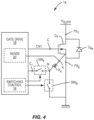
- the purpose of the additional sense resistor R sa is to prevent current from flowing from the gate drive circuitry 16 into the power loop. Accordingly, the functionality of the additional sense resistor R sa could also be accomplished by a sense switching element SW s as shown in Figure 4 .
- the switching control circuitry 18 may operate the sense switching element SW s in a complementary fashion to the feedback switching element SW fb such that when the feedback switching element SW fb is closed, the sense switching element SW s is open, and vice versa.
- the sense circuitry 20 shown in Figures 4 and 5 is merely exemplary.
- the present disclosure proposes providing a parallel current path to the power loop with a much smaller current than the power loop and measuring the current in the parallel current path to detect overcurrent events. This may be accomplished in many different ways, all of which are contemplated herein.
- external circuitry may be provided and operated to protect the power transistor.
- the gate drive circuitry 16 may change the control signal CNT based on the detection of an overcurrent event. For example, on detection of an overcurrent event when the power transistor Q 1 is operating in the first quadrant mode of operation, the control signal CNT may be provided to cause the power transistor Q 1 to partially or fully enter a blocking mode of operation.
- the control signal CNT may be provided to cause the power transistor Q 1 to enter a conduction mode of operation. This may enable the reverse current through the freewheeling diode D fw to be partially or entirely shared by the power transistor Q 1 , thereby increasing current carrying capacity in the reverse direction and reducing power dissipation such that the overcurrent withstand time of the power transistor Q 1 and the freewheeling diode D fw (and other paralleled devices that are not shown) is increased, sometimes indefinitely.
- FIG. 5 shows the gate drive system 14 according to an additional embodiment of the present disclosure.
- the gate drive system 14 shown in Figure 5 is substantially similar to that shown in Figure 3 , but further includes a first overcurrent protection switching element SW op1 , a second overcurrent protection switching element SW op2 , and an overcurrent protection diode D op .
- the overcurrent protection diode D op is coupled between the intermediate node IN and an additional intermediate node IN a .
- the first overcurrent protection switching element SW op1 is coupled between the additional intermediate node IN a and the control node CNT.
- the second overcurrent protection switching element SW op2 is coupled between the control node CNT and a predetermined voltage V pd .
- the switching control circuitry 18 is coupled to the first overcurrent protection switching element SW op1 and the second overcurrent protection switching element SW op2 .
- the switching control circuitry 18 may cause the first overcurrent protection switching element SW op1 to close and the second overcurrent protection switching element SW op2 to open, thus coupling the intermediate node IN to the control node CNT via the overcurrent protection diode D op .
- the switching control circuitry 18 may cause the first overcurrent protection switching element SW op1 to open and the second overcurrent protection switching element SW op2 to close, thus coupling the control node CNT to the predetermined voltage V pd .
- the predetermined voltage V pd may be configured to ensure that the power transistor Q 1 is in a conduction mode of operation such that current can be conducted through a channel thereof. Accordingly, a current from the second power switching node PS 2 to the first power switching node PS 1 can flow through both the freewheeling diode D fw and the channel of the power transistor Q 1 .
- the power transistor Q 1 may be any suitable type of power transistor such as an insulated gate bipolar transistor (IGBT). Specifically, the power transistor Q 1 may be a reverse conducting IGBT (RC-IGBT).
- Figure 6 shows the gate drive system 14 wherein the power transistor Q 1 is an IGBT.
- the gate drive system 10 is substantially similar to that shown in Figure 5 .
- the power transistor Q 1 includes a semiconductor structure between the control node, the first power switching node PS 1 , the second power switching node PS 2 , and the Kelvin connection node K such that a control signal CNT provided between the control node C and the Kelvin connection node K varies a resistance between the first power switching node PS 1 and the second power switching node PS 2 .
- the control node C is coupled to a gate region in the semiconductor structure
- the first power switching node PS 1 is coupled to a collector region and a cathode region in the semiconductor structure
- the second power switching node PS 2 and the Kelvin connection node are coupled to an emitter region and an anode region in the semiconductor structure.
- FIG. 7 is a flow diagram illustrating a method for providing overcurrent protection for a power transistor according to one embodiment of the present disclosure.
- a control signal is provided between a control node and a Kelvin connection node of a power transistor (step 100).
- a resistance between a first power switching node and a second power switching node of the power transistor is based on the control signal.
- the Kelvin connection node is coupled to the second power switching node after the control signal is provided such that the power transistor is switched from a blocking mode of operation to a conduction mode of operation (step 102).
- the Kelvin connection node Before providing the control signal such that the power transistor is switched from the conduction mode of operation to the blocking mode of operation, the Kelvin connection node is isolated from the second power switching node (step 104). As discussed above, coupling the Kelvin connection node to the second power switching node introduces feedback between the control loop and the power loop that partially turns off the power transistor in the event of an overcurrent event and thus increases a short circuit withstand time of the power transistor. Isolating the Kelvin connection node from the second power switching node before switching the power transistor from the conduction mode of operation to the blocking mode of operation maintains the switching speed of the power transistor. Further as discussed above, the power transistor may be a MOSFET, an IGBT, or any other suitable power transistor.
- the conduction mode of operation may include a first quadrant mode of operation or a third quadrant mode of operation. In some embodiments, the conduction mode may include a second quadrant mode of operation or a fourth quadrant mode of operation.
- the Kelvin connection node is coupled to the second power switching node at least 5 picoseconds after the control signal is provided such that the power transistor is switched from the blocking mode to the conduction mode. Generally, the Kelvin connection node may be coupled to the second power switching mode anywhere between 5 picoseconds and 500 microseconds after the control signal is provided such that the power transistor is switched from the blocking mode to the conduction mode. Notably, these timing values are merely exemplary.
- the Kelvin connection node is isolated from the second power switching node at least 5 picoseconds before the control signal is provided such that the power transistor is switched from the conduction mode to the blocking mode.
- the Kelvin connection node may be isolated from the second power switching node anywhere between 5 picoseconds and 500 microseconds before the control signal is provided such that the power transistor is switched from the conduction mode to the blocking mode.
- these timing values are merely exemplary.
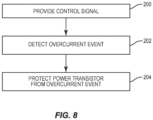
- FIG. 8 is a flow diagram illustrating a method for measuring an overcurrent event according to one embodiment of the present disclosure.
- a control signal is provided between a control node and a Kelvin node of a power transistor, wherein a resistance between a first power switching node and a second power switching node of the power transistor is based on the control signal (step 200).
- An overcurrent event is detected based on a signal measured at the Kelvin connection node of the power transistor (step 202).
- an overcurrent event is detected based on a signal measured in the control loop of the power transistor, or in a parallel current path to the power loop that provides a current that is proportional to the power loop.
- the power transistor is protected from the overcurrent event (step 204).
- the overcurrent event may be detected by measuring a voltage across a sense resistor coupled to the Kelvin connection node.
- the power transistor may be protected from the overcurrent event by partially or fully turning off the power transistor when the power transistor is operating in the first quadrant mode of operation or by partially or fully turning on the power transistor when the power transistor is operating in a third quadrant mode of operation. Further, any devices coupled in parallel with the power transistor (e.g., freewheeling diodes, etc.) will also be protected from overcurrent events.
Landscapes
- Engineering & Computer Science (AREA)
- Power Engineering (AREA)
- Power Conversion In General (AREA)
- Electronic Switches (AREA)
Claims (15)
- Unterstützungsschaltung für einen Leistungstransistor (Q1), wobei der Leistungstransistor (Q1) einen Steuerknoten (C), einen Kelvin-Verbindungsknoten (K), einen ersten Leistungsschaltknoten (PS1), einen zweiten Leistungsschaltknoten (PS2) und eine solche Halbleiterstruktur zwischen dem Steuerknoten (C), dem Kelvin-Verbindungsknoten (K), dem ersten Leistungsschaltknoten (PS1) und dem zweiten Leistungsschaltknoten (PS2) umfasst, dass ein Widerstand zwischen dem ersten Leistungsschaltknoten (PS1) und dem zweiten Leistungsschaltknoten (PS2) auf einem zwischen dem Steuerknoten (C) und dem Kelvin-Verbindungsknoten (K) bereitgestellten Steuersignal basiert, wobei die Unterstützungsschaltung umfasst:ein Rückkopplungsschaltelement (SWfb), das zwischen dem Kelvin-Verbindungsknoten (K) und dem zweiten Leistungsschaltknoten (PS2) gekoppelt ist; undeine Schaltsteuerschaltung (18), die mit dem Rückkopplungsschaltelement (SWfb) gekoppelt ist, wobei die Schaltsteuerschaltung (18) konfiguriert ist, umdas Rückkopplungsschaltelement (SWfb) zu veranlassen, nach Umschalten des Leistungstransistors (Q1) von einem Sperrbetrieb in einen Leitungsbetrieb den Kelvin-Verbindungsknoten (K) mit dem zweiten Leistungsschaltknoten (PS2) zu koppeln; unddas Rückkopplungsschaltelement (SWfb) zu veranlassen, vor Umschalten des Leistungstransistors (Q1) von dem Leitungsbetriebsmodus in den Sperrbetriebsmodus den Kelvin-Verbindungsknoten (K) von dem zweiten Leistungsschaltknoten (PS2) zu trennen.
- Unterstützungsschaltung nach Anspruch 1, bei der der Leistungstransistor (Q1) ein Metall-Oxid-Halbleiter-Feldeffekttransistor, MOSFET, ist, der die Halbleiterstruktur zwischen dem Steuerknoten (C), dem Kelvin-Verbindungsknoten (K), dem ersten Leistungsschaltknoten (PS1) und dem zweiten Leistungsschaltknoten (PS2) umfasst, so dass der Steuerknoten (C) mit einem Gatebereich der Halbleiterstruktur gekoppelt ist, der erste Leistungsschaltknoten (PS1) mit einem Drainbereich der Halbleiterstruktur gekoppelt ist und der zweite Leistungsschaltknoten (PS2) und der Kelvin-Verbindungsknoten (K) mit einem Sourcebereich der Halbleiterstruktur gekoppelt sind.
- Unterstützungsschaltung nach Anspruch 2, die ferner den Leistungstransistor (Q1) umfasst.
- Unterstützungsschaltung nach Anspruch 1, bei der der Leistungstransistor (Q1) ein Bipolartransistor mit isoliertem Gate (IGBT) ist, der die Halbleiterstruktur zwischen dem Steuerknoten (C), dem Kelvin-Verbindungsknoten (K), dem ersten Leistungsschaltknoten (PS1) und dem zweiten Leistungsschaltknoten (PS2) umfasst, so dass der Steuerknoten (C) mit einem Gatebereich der Halbleiterstruktur gekoppelt ist, der erste Leistungsschaltknoten (PS1) mit einem Kollektorbereich der Halbleiterstruktur gekoppelt ist und der zweite Leistungsschaltknoten (PS2) und der Kelvin-Verbindungsknoten (K) mit einem Emitterbereich der Halbleiterstruktur gekoppelt sind.
- Unterstützungsschaltung nach Anspruch 4, die ferner den Leistungstransistor (Q1) umfasst.
- Unterstützungsschaltung nach Anspruch 1, bei der der Leitungsbetriebsmodus ein Erster-Quadrant-Betriebsmodus oder ein Dritter-Quadrant-Betriebsmodus ist.
- Unterstützungsschaltung nach Anspruch 1, die ferner einen Messwiderstand (RS) umfasst, der zwischen dem Kelvin-Verbindungsknoten (K) des Leistungstransistors (Q1) und einem Zwischenknoten (IN) gekoppelt ist, wobei das Rückkopplungsschaltelement (SWfb) zwischen dem Zwischenknoten (IN) und dem zweiten Leistungsschaltknoten (PS2) gekoppelt ist.
- Unterstützungsschaltung nach Anspruch 7, die ferner eine Erfassungsschaltung (20) umfasst, die konfiguriert ist, um ein Überstromereignis auf der Grundlage einer Spannung über dem Messwiderstand (RS) zu erfassen.
- Unterstützungsschaltung nach Anspruch 7, die ferner einen zusätzlichen Messwiderstand (Rsa) umfasst, der zwischen dem Zwischenknoten (IN) und einem Steuerrückkopplungsknoten (Cr) gekoppelt ist, wobei das Steuersignal zwischen dem Steuerknoten (C) und dem Steuerrückkopplungsknoten (Cr) bereitgestellt wird.
- Unterstützungsschaltung nach Anspruch 9, die ferner eine Erfassungsschaltung (20) umfasst, die konfiguriert ist, um ein Überstromereignis auf der Grundlage einer Spannung über dem Messwiderstand (RS) und dem zusätzlichen Messwiderstand (Rsa) zu erfassen.
- Unterstützungsschaltung nach Anspruch 7, die ferner ein Messschaltelement (SWS) umfasst, das zwischen dem Zwischenknoten (IN) und einem Steuerrückkopplungsknoten (Cr) gekoppelt ist, wobei:das Steuersignal zwischen dem Steuerknoten (C) und dem Steuerrückkopplungsknoten (Cr) bereitgestellt wird; unddie Schaltsteuerschaltung (18) ferner konfiguriert ist, um das Messschaltelement (SWS) komplementär zu dem Rückkopplungsschaltelement (SWfb) zu betreiben.
- Unterstützungsschaltung nach Anspruch 11, die ferner eine Messschaltung (20) umfasst, die konfiguriert ist, um ein Überstromereignis auf der Grundlage einer Spannung über dem Messwiderstand (RS) zu erfassen.
- Unterstützungsschaltung nach Anspruch 12, die ferner umfasst:ein erstes Überstromschutz-Schaltelement (SWop1), das zwischen dem Steuerknoten (C) und einem zusätzlichen Zwischenknoten (INa) gekoppelt ist;eine Überstromschutzdiode (Dop) mit einer Anode, die mit dem Zwischenknoten (IN) und dem zusätzlichen Zwischenknoten (INa) gekoppelt ist; undein zweites Überstromschutz-Schaltelement (SWop2), das zwischen einer vorgegebenen Spannung und dem Steuerknoten (C) gekoppelt ist, wobeidie Schaltsteuerschaltung (18) ferner konfiguriert ist, um das erste Überstromschutz-Schaltelement (SWop1) zu veranlassen, den Steuerknoten (C) mit dem zusätzlichen Zwischenknoten (INa) zu koppeln, und das zweite Überstromschutz-Schaltelement (SWop2) zu veranlassen, den Steuerknoten (C) von der vorgegebenen Spannung zu trennen, wenn ein Überstromereignis erkannt wird,wobei die Schaltsteuerschaltung (18) ferner konfiguriert ist, um das erste Überstromschutz-Schaltelement (SWop1) zu veranlassen, den Steuerknoten (C) von dem zusätzlichen Zwischenknoten (INa) zu trennen, und das zweite Überstromschutz-Schaltelement (SWop2) zu veranlassen, den Steuerknoten (C) mit der vorgegebenen Spannung zu koppeln, wobei die vorgegebene Spannung ausreicht, um einen Kanal des Leistungstransistors (Q1) zum Leiten von Strom zu veranlassen, so dass ein Strom vom zweiten Leistungsschaltknoten (PS2) zum ersten Leistungsschaltknoten (PS1) durch den Kanal des Leistungstransistors (Q1) fließt, wenn der Leistungstransistor (Q1) in einem Dritter-Quadrant-Betriebsmodus arbeitet.
- Verfahren zum Betreiben eines die Unterstützungsschaltung nach Anspruch 1 und einen Leistungstransistor (Q1) umfassenden Systems (14), wobei das Verfahren umfasst:• Bereitstellen eines Steuersignals zwischen dem Steuerknoten und dem Kelvin-Verbindungsknoten des Leistungstransistors;• nach dem Bereitstellen des Steuersignals derart, dass der Leistungstransistor von einem Sperrbetrieb in einen Leitungsbetrieb geschaltet wird, Koppeln des Kelvin-Verbindungsknotens mit dem zweiten Leistungsschaltknoten; und• vor dem Bereitstellen des Steuersignals derart, dass der Leistungstransistor von dem Leitungsbetrieb in den Sperrbetrieb geschaltet wird, Trennen des Kelvin-Verbindungsknotens von dem zweiten Leistungsschaltknoten.
- Verfahren zum Betreiben eines die Unterstützungsschaltung nach Anspruch 1 und einen Leistungstransistor (Q1) umfassenden Systems (14), wobei das Verfahren umfasst:• Bereitstellen eines Steuersignals zwischen dem Steuerknoten und dem Kelvin-Verbindungsknoten des Leistungstransistors;• Erkennen eines Überstromereignisses auf der Grundlage eines am Kelvin-Verbindungsknoten des Leistungstransistors gemessenen Signals; und• als Reaktion auf die Erkennung des Überstromereignisses, Schützen des Leistungstransistors vor dem Überstromereignis.
Applications Claiming Priority (2)
| Application Number | Priority Date | Filing Date | Title |
|---|---|---|---|
| US16/524,726 US11139810B2 (en) | 2019-07-29 | 2019-07-29 | Overcurrent protection for power transistors |
| PCT/US2020/043196 WO2021021541A1 (en) | 2019-07-29 | 2020-07-23 | Overcurrent protection for power transistors |
Publications (2)
| Publication Number | Publication Date |
|---|---|
| EP4005093A1 EP4005093A1 (de) | 2022-06-01 |
| EP4005093B1 true EP4005093B1 (de) | 2024-12-11 |
Family
ID=71995178
Family Applications (1)
| Application Number | Title | Priority Date | Filing Date |
|---|---|---|---|
| EP20753641.8A Active EP4005093B1 (de) | 2019-07-29 | 2020-07-23 | Überstromschutz für leistungstransistoren |
Country Status (4)
| Country | Link |
|---|---|
| US (1) | US11139810B2 (de) |
| EP (1) | EP4005093B1 (de) |
| CN (1) | CN114175435A (de) |
| WO (1) | WO2021021541A1 (de) |
Families Citing this family (3)
| Publication number | Priority date | Publication date | Assignee | Title |
|---|---|---|---|---|
| JP7292874B2 (ja) * | 2018-12-26 | 2023-06-19 | 株式会社東芝 | 電流検出回路 |
| DE102019208122A1 (de) * | 2019-06-04 | 2020-12-10 | Audi Ag | Verfahren zum Betrieb einer elektrischen Schaltung, elektrische Schaltung und Kraftfahrzeug |
| US20250323639A1 (en) * | 2024-04-16 | 2025-10-16 | Semiconductor Components Industries, Llc | Asymmetric common source inductances to reduce turn-off overvoltage in mosfets |
Family Cites Families (12)
| Publication number | Priority date | Publication date | Assignee | Title |
|---|---|---|---|---|
| US4945445A (en) * | 1988-09-29 | 1990-07-31 | Gentron Corporation | Current sense circuit |
| US5191297A (en) * | 1991-07-25 | 1993-03-02 | Iomega Corporation | Transconductance amplifier having sensfets which drive a load with linearly proportional current |
| US5495154A (en) * | 1993-04-29 | 1996-02-27 | Sgs-Thomson Microelectronics, Inc. | Method and apparatus for Kelvin current sensing in a multi-phase driver for a polyphase DC motor |
| JP3132648B2 (ja) | 1996-09-20 | 2001-02-05 | 富士電機株式会社 | 電力変換器におけるゲート駆動回路 |
| US6127746A (en) * | 1996-10-21 | 2000-10-03 | International Rectifier Corp. | Method of controlling the switching DI/DT and DV/DT of a MOS-gated power transistor |
| EP1191692A4 (de) | 2000-02-25 | 2003-05-14 | Mitsubishi Electric Corp | Leistungsmodel |
| EP2495875A4 (de) | 2009-10-26 | 2013-12-18 | Nissan Motor | Treiberschaltung für ein schaltelement und stromumrichter damit |
| JP6155779B2 (ja) | 2013-04-09 | 2017-07-05 | 株式会社デンソー | パワー素子の電流検出回路 |
| EP2843425B1 (de) * | 2013-08-27 | 2018-11-21 | Nxp B.V. | Strommesskreis |
| US10008846B2 (en) * | 2015-10-20 | 2018-06-26 | Nxp B.V. | Control device for an electronic fuse and method for controlling an electronic fuse |
| EP3174205A1 (de) * | 2015-11-27 | 2017-05-31 | ABB Technology Oy | Steuerungsschaltung mit rückkopplung |
| US9991880B2 (en) * | 2016-06-07 | 2018-06-05 | Ford Global Technologies, Llc | Discrete power switching devices with reduced common source inductance |
-
2019
- 2019-07-29 US US16/524,726 patent/US11139810B2/en active Active
-
2020
- 2020-07-23 CN CN202080054206.6A patent/CN114175435A/zh active Pending
- 2020-07-23 WO PCT/US2020/043196 patent/WO2021021541A1/en not_active Ceased
- 2020-07-23 EP EP20753641.8A patent/EP4005093B1/de active Active
Also Published As
| Publication number | Publication date |
|---|---|
| US11139810B2 (en) | 2021-10-05 |
| EP4005093A1 (de) | 2022-06-01 |
| US20210036696A1 (en) | 2021-02-04 |
| CN114175435A (zh) | 2022-03-11 |
| WO2021021541A1 (en) | 2021-02-04 |
Similar Documents
| Publication | Publication Date | Title |
|---|---|---|
| US9203393B2 (en) | Semiconductor apparatus | |
| US7737761B2 (en) | Gate drive circuit with reduced switching loss and noise | |
| EP0402928B1 (de) | Schaltung zur internen Strombegrenzung für schnellen Leistungsschalter | |
| EP0706265B1 (de) | Stromdetektorschaltung | |
| US9184158B2 (en) | Semiconductor device having diode-built-in IGBT and semiconductor device having diode-built-in DMOS | |
| CN107615664B (zh) | 功率晶体管驱动装置 | |
| EP4005093B1 (de) | Überstromschutz für leistungstransistoren | |
| US20180375508A1 (en) | Power switching apparatus | |
| EP1028526B1 (de) | Schaltungsanordnung mit Schwachstromdetektion | |
| CN110311664B (zh) | 驱动装置以及功率模块 | |
| US11942927B2 (en) | Method and device for short-circuit detection by saturation detection in power semiconductor switches | |
| US5909135A (en) | High-side MOSFET gate protection shunt circuit | |
| US5561391A (en) | Clamp circuit and method for detecting an activation of same | |
| US20130314834A1 (en) | Semiconductor driving circuit and semiconductor device | |
| US6441679B1 (en) | Semiconductor active fuse operating at higher supply voltage employing current oscillation | |
| JP7508906B2 (ja) | 電子回路及び半導体モジュール | |
| JP5630484B2 (ja) | 半導体装置 | |
| US20250247089A1 (en) | Power Device, Electronic Device, and Circuit Structure | |
| EP3731413A1 (de) | Gate-treiberschaltung und verfahren zur ansteuerung eines gates eines feldeffekttransistors | |
| US7489490B2 (en) | Current limiting MOSFET structure for solid state relays | |
| JP7206976B2 (ja) | スイッチング回路 | |
| US12451880B2 (en) | On-state voltage measurement circuit | |
| JP7774518B2 (ja) | 短絡保護回路、半導体装置、及び短絡保護方法 | |
| JP2010246179A (ja) | 半導体装置 |
Legal Events
| Date | Code | Title | Description |
|---|---|---|---|
| STAA | Information on the status of an ep patent application or granted ep patent |
Free format text: STATUS: UNKNOWN |
|
| STAA | Information on the status of an ep patent application or granted ep patent |
Free format text: STATUS: THE INTERNATIONAL PUBLICATION HAS BEEN MADE |
|
| PUAI | Public reference made under article 153(3) epc to a published international application that has entered the european phase |
Free format text: ORIGINAL CODE: 0009012 |
|
| STAA | Information on the status of an ep patent application or granted ep patent |
Free format text: STATUS: REQUEST FOR EXAMINATION WAS MADE |
|
| 17P | Request for examination filed |
Effective date: 20220106 |
|
| AK | Designated contracting states |
Kind code of ref document: A1 Designated state(s): AL AT BE BG CH CY CZ DE DK EE ES FI FR GB GR HR HU IE IS IT LI LT LU LV MC MK MT NL NO PL PT RO RS SE SI SK SM TR |
|
| DAV | Request for validation of the european patent (deleted) | ||
| DAX | Request for extension of the european patent (deleted) | ||
| GRAP | Despatch of communication of intention to grant a patent |
Free format text: ORIGINAL CODE: EPIDOSNIGR1 |
|
| STAA | Information on the status of an ep patent application or granted ep patent |
Free format text: STATUS: GRANT OF PATENT IS INTENDED |
|
| INTG | Intention to grant announced |
Effective date: 20240708 |
|
| GRAS | Grant fee paid |
Free format text: ORIGINAL CODE: EPIDOSNIGR3 |
|
| GRAA | (expected) grant |
Free format text: ORIGINAL CODE: 0009210 |
|
| STAA | Information on the status of an ep patent application or granted ep patent |
Free format text: STATUS: THE PATENT HAS BEEN GRANTED |
|
| P01 | Opt-out of the competence of the unified patent court (upc) registered |
Free format text: CASE NUMBER: APP_57890/2024 Effective date: 20241023 |
|
| AK | Designated contracting states |
Kind code of ref document: B1 Designated state(s): AL AT BE BG CH CY CZ DE DK EE ES FI FR GB GR HR HU IE IS IT LI LT LU LV MC MK MT NL NO PL PT RO RS SE SI SK SM TR |
|
| REG | Reference to a national code |
Ref country code: GB Ref legal event code: FG4D |
|
| REG | Reference to a national code |
Ref country code: CH Ref legal event code: EP |
|
| REG | Reference to a national code |
Ref country code: DE Ref legal event code: R096 Ref document number: 602020042981 Country of ref document: DE |
|
| REG | Reference to a national code |
Ref country code: IE Ref legal event code: FG4D |
|
| REG | Reference to a national code |
Ref country code: LT Ref legal event code: MG9D |
|
| PG25 | Lapsed in a contracting state [announced via postgrant information from national office to epo] |
Ref country code: HR Free format text: LAPSE BECAUSE OF FAILURE TO SUBMIT A TRANSLATION OF THE DESCRIPTION OR TO PAY THE FEE WITHIN THE PRESCRIBED TIME-LIMIT Effective date: 20241211 |
|
| PG25 | Lapsed in a contracting state [announced via postgrant information from national office to epo] |
Ref country code: FI Free format text: LAPSE BECAUSE OF FAILURE TO SUBMIT A TRANSLATION OF THE DESCRIPTION OR TO PAY THE FEE WITHIN THE PRESCRIBED TIME-LIMIT Effective date: 20241211 |
|
| PG25 | Lapsed in a contracting state [announced via postgrant information from national office to epo] |
Ref country code: BG Free format text: LAPSE BECAUSE OF FAILURE TO SUBMIT A TRANSLATION OF THE DESCRIPTION OR TO PAY THE FEE WITHIN THE PRESCRIBED TIME-LIMIT Effective date: 20241211 |
|
| REG | Reference to a national code |
Ref country code: NL Ref legal event code: MP Effective date: 20241211 |
|
| PG25 | Lapsed in a contracting state [announced via postgrant information from national office to epo] |
Ref country code: ES Free format text: LAPSE BECAUSE OF FAILURE TO SUBMIT A TRANSLATION OF THE DESCRIPTION OR TO PAY THE FEE WITHIN THE PRESCRIBED TIME-LIMIT Effective date: 20241211 |
|
| PG25 | Lapsed in a contracting state [announced via postgrant information from national office to epo] |
Ref country code: NO Free format text: LAPSE BECAUSE OF FAILURE TO SUBMIT A TRANSLATION OF THE DESCRIPTION OR TO PAY THE FEE WITHIN THE PRESCRIBED TIME-LIMIT Effective date: 20250311 |
|
| PG25 | Lapsed in a contracting state [announced via postgrant information from national office to epo] |
Ref country code: LV Free format text: LAPSE BECAUSE OF FAILURE TO SUBMIT A TRANSLATION OF THE DESCRIPTION OR TO PAY THE FEE WITHIN THE PRESCRIBED TIME-LIMIT Effective date: 20241211 Ref country code: GR Free format text: LAPSE BECAUSE OF FAILURE TO SUBMIT A TRANSLATION OF THE DESCRIPTION OR TO PAY THE FEE WITHIN THE PRESCRIBED TIME-LIMIT Effective date: 20250312 |
|
| PG25 | Lapsed in a contracting state [announced via postgrant information from national office to epo] |
Ref country code: RS Free format text: LAPSE BECAUSE OF FAILURE TO SUBMIT A TRANSLATION OF THE DESCRIPTION OR TO PAY THE FEE WITHIN THE PRESCRIBED TIME-LIMIT Effective date: 20250311 |
|
| PG25 | Lapsed in a contracting state [announced via postgrant information from national office to epo] |
Ref country code: NL Free format text: LAPSE BECAUSE OF FAILURE TO SUBMIT A TRANSLATION OF THE DESCRIPTION OR TO PAY THE FEE WITHIN THE PRESCRIBED TIME-LIMIT Effective date: 20241211 |
|
| REG | Reference to a national code |
Ref country code: AT Ref legal event code: MK05 Ref document number: 1751170 Country of ref document: AT Kind code of ref document: T Effective date: 20241211 |
|
| PG25 | Lapsed in a contracting state [announced via postgrant information from national office to epo] |
Ref country code: SM Free format text: LAPSE BECAUSE OF FAILURE TO SUBMIT A TRANSLATION OF THE DESCRIPTION OR TO PAY THE FEE WITHIN THE PRESCRIBED TIME-LIMIT Effective date: 20241211 |
|
| PG25 | Lapsed in a contracting state [announced via postgrant information from national office to epo] |
Ref country code: PL Free format text: LAPSE BECAUSE OF FAILURE TO SUBMIT A TRANSLATION OF THE DESCRIPTION OR TO PAY THE FEE WITHIN THE PRESCRIBED TIME-LIMIT Effective date: 20241211 |
|
| PG25 | Lapsed in a contracting state [announced via postgrant information from national office to epo] |
Ref country code: IS Free format text: LAPSE BECAUSE OF FAILURE TO SUBMIT A TRANSLATION OF THE DESCRIPTION OR TO PAY THE FEE WITHIN THE PRESCRIBED TIME-LIMIT Effective date: 20250411 |
|
| PG25 | Lapsed in a contracting state [announced via postgrant information from national office to epo] |
Ref country code: PT Free format text: LAPSE BECAUSE OF FAILURE TO SUBMIT A TRANSLATION OF THE DESCRIPTION OR TO PAY THE FEE WITHIN THE PRESCRIBED TIME-LIMIT Effective date: 20250411 |
|
| PG25 | Lapsed in a contracting state [announced via postgrant information from national office to epo] |
Ref country code: EE Free format text: LAPSE BECAUSE OF FAILURE TO SUBMIT A TRANSLATION OF THE DESCRIPTION OR TO PAY THE FEE WITHIN THE PRESCRIBED TIME-LIMIT Effective date: 20241211 |
|
| PG25 | Lapsed in a contracting state [announced via postgrant information from national office to epo] |
Ref country code: RO Free format text: LAPSE BECAUSE OF FAILURE TO SUBMIT A TRANSLATION OF THE DESCRIPTION OR TO PAY THE FEE WITHIN THE PRESCRIBED TIME-LIMIT Effective date: 20241211 Ref country code: AT Free format text: LAPSE BECAUSE OF FAILURE TO SUBMIT A TRANSLATION OF THE DESCRIPTION OR TO PAY THE FEE WITHIN THE PRESCRIBED TIME-LIMIT Effective date: 20241211 |
|
| PG25 | Lapsed in a contracting state [announced via postgrant information from national office to epo] |
Ref country code: SK Free format text: LAPSE BECAUSE OF FAILURE TO SUBMIT A TRANSLATION OF THE DESCRIPTION OR TO PAY THE FEE WITHIN THE PRESCRIBED TIME-LIMIT Effective date: 20241211 |
|
| PG25 | Lapsed in a contracting state [announced via postgrant information from national office to epo] |
Ref country code: CZ Free format text: LAPSE BECAUSE OF FAILURE TO SUBMIT A TRANSLATION OF THE DESCRIPTION OR TO PAY THE FEE WITHIN THE PRESCRIBED TIME-LIMIT Effective date: 20241211 |
|
| PG25 | Lapsed in a contracting state [announced via postgrant information from national office to epo] |
Ref country code: IT Free format text: LAPSE BECAUSE OF FAILURE TO SUBMIT A TRANSLATION OF THE DESCRIPTION OR TO PAY THE FEE WITHIN THE PRESCRIBED TIME-LIMIT Effective date: 20241211 |
|
| PG25 | Lapsed in a contracting state [announced via postgrant information from national office to epo] |
Ref country code: SE Free format text: LAPSE BECAUSE OF FAILURE TO SUBMIT A TRANSLATION OF THE DESCRIPTION OR TO PAY THE FEE WITHIN THE PRESCRIBED TIME-LIMIT Effective date: 20241211 |
|
| REG | Reference to a national code |
Ref country code: DE Ref legal event code: R097 Ref document number: 602020042981 Country of ref document: DE |
|
| PG25 | Lapsed in a contracting state [announced via postgrant information from national office to epo] |
Ref country code: DK Free format text: LAPSE BECAUSE OF FAILURE TO SUBMIT A TRANSLATION OF THE DESCRIPTION OR TO PAY THE FEE WITHIN THE PRESCRIBED TIME-LIMIT Effective date: 20241211 |
|
| PGFP | Annual fee paid to national office [announced via postgrant information from national office to epo] |
Ref country code: DE Payment date: 20250729 Year of fee payment: 6 |
|
| PGFP | Annual fee paid to national office [announced via postgrant information from national office to epo] |
Ref country code: GB Payment date: 20250728 Year of fee payment: 6 |
|
| PLBE | No opposition filed within time limit |
Free format text: ORIGINAL CODE: 0009261 |
|
| STAA | Information on the status of an ep patent application or granted ep patent |
Free format text: STATUS: NO OPPOSITION FILED WITHIN TIME LIMIT |
|
| PGFP | Annual fee paid to national office [announced via postgrant information from national office to epo] |
Ref country code: FR Payment date: 20250725 Year of fee payment: 6 |
|
| PGFP | Annual fee paid to national office [announced via postgrant information from national office to epo] |
Ref country code: CH Payment date: 20250801 Year of fee payment: 6 |
|
| 26N | No opposition filed |
Effective date: 20250912 |
|
| PG25 | Lapsed in a contracting state [announced via postgrant information from national office to epo] |
Ref country code: LU Free format text: LAPSE BECAUSE OF NON-PAYMENT OF DUE FEES Effective date: 20250723 |
|
| REG | Reference to a national code |
Ref country code: BE Ref legal event code: MM Effective date: 20250731 |
|
| PG25 | Lapsed in a contracting state [announced via postgrant information from national office to epo] |
Ref country code: BE Free format text: LAPSE BECAUSE OF NON-PAYMENT OF DUE FEES Effective date: 20250731 |