EP4005097B1 - Empfängerschaltungen mit einem blockerdämpfenden rf-filter - Google Patents
Empfängerschaltungen mit einem blockerdämpfenden rf-filter Download PDFInfo
- Publication number
- EP4005097B1 EP4005097B1 EP21743857.1A EP21743857A EP4005097B1 EP 4005097 B1 EP4005097 B1 EP 4005097B1 EP 21743857 A EP21743857 A EP 21743857A EP 4005097 B1 EP4005097 B1 EP 4005097B1
- Authority
- EP
- European Patent Office
- Prior art keywords
- signal
- filter
- response
- amplifier
- clipping
- Prior art date
- Legal status (The legal status is an assumption and is not a legal conclusion. Google has not performed a legal analysis and makes no representation as to the accuracy of the status listed.)
- Active
Links
Images

Classifications
-
- H—ELECTRICITY
- H04—ELECTRIC COMMUNICATION TECHNIQUE
- H04L—TRANSMISSION OF DIGITAL INFORMATION, e.g. TELEGRAPHIC COMMUNICATION
- H04L27/00—Modulated-carrier systems
- H04L27/10—Frequency-modulated carrier systems, i.e. using frequency-shift keying
- H04L27/14—Demodulator circuits; Receiver circuits
-
- H—ELECTRICITY
- H04—ELECTRIC COMMUNICATION TECHNIQUE
- H04L—TRANSMISSION OF DIGITAL INFORMATION, e.g. TELEGRAPHIC COMMUNICATION
- H04L27/00—Modulated-carrier systems
- H04L27/32—Carrier systems characterised by combinations of two or more of the types covered by groups H04L27/02, H04L27/10, H04L27/18 or H04L27/26
- H04L27/34—Amplitude- and phase-modulated carrier systems, e.g. quadrature-amplitude modulated carrier systems
- H04L27/36—Modulator circuits; Transmitter circuits
- H04L27/366—Arrangements for compensating undesirable properties of the transmission path between the modulator and the demodulator
- H04L27/367—Arrangements for compensating undesirable properties of the transmission path between the modulator and the demodulator using predistortion
- H04L27/368—Arrangements for compensating undesirable properties of the transmission path between the modulator and the demodulator using predistortion adaptive predistortion
-
- H—ELECTRICITY
- H03—ELECTRONIC CIRCUITRY
- H03F—AMPLIFIERS
- H03F3/00—Amplifiers with only discharge tubes or only semiconductor devices as amplifying elements
- H03F3/189—High-frequency amplifiers, e.g. radio frequency amplifiers
-
- H—ELECTRICITY
- H03—ELECTRONIC CIRCUITRY
- H03F—AMPLIFIERS
- H03F3/00—Amplifiers with only discharge tubes or only semiconductor devices as amplifying elements
- H03F3/20—Power amplifiers, e.g. Class B amplifiers, Class C amplifiers
- H03F3/21—Power amplifiers, e.g. Class B amplifiers, Class C amplifiers with semiconductor devices only
- H03F3/211—Power amplifiers, e.g. Class B amplifiers, Class C amplifiers with semiconductor devices only using a combination of several amplifiers
-
- H—ELECTRICITY
- H03—ELECTRONIC CIRCUITRY
- H03F—AMPLIFIERS
- H03F3/00—Amplifiers with only discharge tubes or only semiconductor devices as amplifying elements
- H03F3/72—Gated amplifiers, i.e. amplifiers which are rendered operative or inoperative by means of a control signal
-
- H—ELECTRICITY
- H04—ELECTRIC COMMUNICATION TECHNIQUE
- H04B—TRANSMISSION
- H04B1/00—Details of transmission systems, not covered by a single one of groups H04B3/00 - H04B13/00; Details of transmission systems not characterised by the medium used for transmission
- H04B1/06—Receivers
- H04B1/10—Means associated with receiver for limiting or suppressing noise or interference
- H04B1/109—Means associated with receiver for limiting or suppressing noise or interference by improving strong signal performance of the receiver when strong unwanted signals are present at the receiver input
-
- H—ELECTRICITY
- H04—ELECTRIC COMMUNICATION TECHNIQUE
- H04B—TRANSMISSION
- H04B1/00—Details of transmission systems, not covered by a single one of groups H04B3/00 - H04B13/00; Details of transmission systems not characterised by the medium used for transmission
- H04B1/06—Receivers
- H04B1/10—Means associated with receiver for limiting or suppressing noise or interference
- H04B1/12—Neutralising, balancing, or compensation arrangements
-
- H—ELECTRICITY
- H04—ELECTRIC COMMUNICATION TECHNIQUE
- H04B—TRANSMISSION
- H04B1/00—Details of transmission systems, not covered by a single one of groups H04B3/00 - H04B13/00; Details of transmission systems not characterised by the medium used for transmission
- H04B1/06—Receivers
- H04B1/16—Circuits
-
- H—ELECTRICITY
- H03—ELECTRONIC CIRCUITRY
- H03F—AMPLIFIERS
- H03F2200/00—Indexing scheme relating to amplifiers
- H03F2200/165—A filter circuit coupled to the input of an amplifier
-
- H—ELECTRICITY
- H03—ELECTRONIC CIRCUITRY
- H03F—AMPLIFIERS
- H03F2200/00—Indexing scheme relating to amplifiers
- H03F2200/294—Indexing scheme relating to amplifiers the amplifier being a low noise amplifier [LNA]
-
- H—ELECTRICITY
- H03—ELECTRONIC CIRCUITRY
- H03F—AMPLIFIERS
- H03F2200/00—Indexing scheme relating to amplifiers
- H03F2200/405—Indexing scheme relating to amplifiers the output amplifying stage of an amplifier comprising more than three power stages
-
- H—ELECTRICITY
- H03—ELECTRONIC CIRCUITRY
- H03F—AMPLIFIERS
- H03F2200/00—Indexing scheme relating to amplifiers
- H03F2200/451—Indexing scheme relating to amplifiers the amplifier being a radio frequency amplifier
-
- H—ELECTRICITY
- H03—ELECTRONIC CIRCUITRY
- H03F—AMPLIFIERS
- H03F2203/00—Indexing scheme relating to amplifiers with only discharge tubes or only semiconductor devices as amplifying elements covered by H03F3/00
- H03F2203/20—Indexing scheme relating to power amplifiers, e.g. Class B amplifiers, Class C amplifiers
- H03F2203/21—Indexing scheme relating to power amplifiers, e.g. Class B amplifiers, Class C amplifiers with semiconductor devices only
- H03F2203/211—Indexing scheme relating to power amplifiers, e.g. Class B amplifiers, Class C amplifiers with semiconductor devices only using a combination of several amplifiers
- H03F2203/21109—An input signal being distributed by switching to a plurality of paralleled power amplifiers
-
- H—ELECTRICITY
- H03—ELECTRONIC CIRCUITRY
- H03F—AMPLIFIERS
- H03F2203/00—Indexing scheme relating to amplifiers with only discharge tubes or only semiconductor devices as amplifying elements covered by H03F3/00
- H03F2203/20—Indexing scheme relating to power amplifiers, e.g. Class B amplifiers, Class C amplifiers
- H03F2203/21—Indexing scheme relating to power amplifiers, e.g. Class B amplifiers, Class C amplifiers with semiconductor devices only
- H03F2203/211—Indexing scheme relating to power amplifiers, e.g. Class B amplifiers, Class C amplifiers with semiconductor devices only using a combination of several amplifiers
- H03F2203/21112—A filter circuit being added at the input of a power amplifier stage
-
- H—ELECTRICITY
- H03—ELECTRONIC CIRCUITRY
- H03F—AMPLIFIERS
- H03F2203/00—Indexing scheme relating to amplifiers with only discharge tubes or only semiconductor devices as amplifying elements covered by H03F3/00
- H03F2203/20—Indexing scheme relating to power amplifiers, e.g. Class B amplifiers, Class C amplifiers
- H03F2203/21—Indexing scheme relating to power amplifiers, e.g. Class B amplifiers, Class C amplifiers with semiconductor devices only
- H03F2203/211—Indexing scheme relating to power amplifiers, e.g. Class B amplifiers, Class C amplifiers with semiconductor devices only using a combination of several amplifiers
- H03F2203/21136—An input signal of a power amplifier being on/off switched
-
- H—ELECTRICITY
- H03—ELECTRONIC CIRCUITRY
- H03F—AMPLIFIERS
- H03F2203/00—Indexing scheme relating to amplifiers with only discharge tubes or only semiconductor devices as amplifying elements covered by H03F3/00
- H03F2203/20—Indexing scheme relating to power amplifiers, e.g. Class B amplifiers, Class C amplifiers
- H03F2203/21—Indexing scheme relating to power amplifiers, e.g. Class B amplifiers, Class C amplifiers with semiconductor devices only
- H03F2203/211—Indexing scheme relating to power amplifiers, e.g. Class B amplifiers, Class C amplifiers with semiconductor devices only using a combination of several amplifiers
- H03F2203/21157—A filter circuit being added at the output of a power amplifier stage
-
- H—ELECTRICITY
- H03—ELECTRONIC CIRCUITRY
- H03F—AMPLIFIERS
- H03F2203/00—Indexing scheme relating to amplifiers with only discharge tubes or only semiconductor devices as amplifying elements covered by H03F3/00
- H03F2203/72—Indexing scheme relating to gated amplifiers, i.e. amplifiers which are rendered operative or inoperative by means of a control signal
- H03F2203/7215—Indexing scheme relating to gated amplifiers, i.e. amplifiers which are rendered operative or inoperative by means of a control signal the gated amplifier being switched on or off by a switch at the input of the amplifier
-
- H—ELECTRICITY
- H03—ELECTRONIC CIRCUITRY
- H03F—AMPLIFIERS
- H03F2203/00—Indexing scheme relating to amplifiers with only discharge tubes or only semiconductor devices as amplifying elements covered by H03F3/00
- H03F2203/72—Indexing scheme relating to gated amplifiers, i.e. amplifiers which are rendered operative or inoperative by means of a control signal
- H03F2203/7236—Indexing scheme relating to gated amplifiers, i.e. amplifiers which are rendered operative or inoperative by means of a control signal the gated amplifier being switched on or off by putting into parallel or not, by choosing between amplifiers by (a ) switch(es)
Definitions
- EP2624463A1 provides a down-conversion circuit (30) for a receiver circuit (10). It comprises a first mixer (70) arranged to down-convert an RF signal with a first LO signal (LO1), thereby generating a first down-converted signal. It further comprises a second mixer (80) arranged to down-convert the RF signal with a second LO signal (LO2) having the same LO frequency as the first LO signal (LO1), but a different and a second duty cycle, thereby generating a second down-converted signal.
- the second mixer (80) has an enabled and a disabled mode.
- the down-conversion circuit (30) also comprises a third mixer (140) arranged to down-convert the RF signal with the second LO signal (LO2), thereby generating a third down-converted signal.
- a passive output combiner network is used to combine the first and the second down-converted signals such that harmonically down-converted signal content present in the first down-converted signal and harmonically down-converted signal content present in the second down-converted signal cancel in a combined output signal of the down-conversion circuit.
- EP0913934A2 discloses a receiving apparatus which can cope with the fluctuation of input level of RF signal appropriately and has a first amplifier means (13) wherein the amplifying and the attenuating of input signal are selectively performed and for processing the signal in a communication band handled by this apparatus, and a second amplifier means (18) for gain-variably amplifying a signal which is a signal converted from the output of the first amplification means 13 into the intermediate frequency signal or base band signal, the gain of the second amplifier means (18) being set based on the detection of output level of the second amplifier means (18), and the selection of the amplification or attenuation in the first amplifier means (13) being performed based on the detection level of output from the first amplifier means (13).
- US2013/0115904A1 discloses method for detect interference, which involves detecting the interference component in the received signal if there is such a component, controlling a band reject filter according to the detected interference component to filter the received signal to suppress the interference component, and synchronizing the receiver to the received signal, wherein the step of detecting the interference component is started before synchronization is achieved. By starting the interference detection without waiting for synchronization to be achieved, rather than following the synchronization, then the interference detection is no longer dependent on the synchronization being achieved.
- FIG. 1 is a schematic diagram of an embodiment of a receiver circuit 100.
- Receiver circuit 100 includes low noise amplifier (LNA) 110, mixer 120 which receives an oscillator signal from oscillator 130, low-pass filter (LPF) 140, variable gain amplifier (VGA) 150, analog-to-digital converter (ADC) 160, and controller 170.
- LNA low noise amplifier
- LPF low-pass filter
- VGA variable gain amplifier
- ADC analog-to-digital converter
- Low noise amplifier 110 is configured to receive a high-frequency carrier signal modulated with a low frequency information signal.
- the received signal may also include a blocker signal, such as a high power signal also modulating the high-frequency carrier signal near the frequency of the information signal.
- Low noise amplifier 110 may be any low noise amplifier or amplifier, as understood by those of skill in the art.
- mixer 120 In response to the output from the low noise amplifier 110 and the oscillator signal, mixer 120 down converts the signal from the low noise amplifier 110.
- the resulting baseband signal includes information of the low frequency information signal and of the blocker signal.
- the baseband signal is then processed by the low-pass filter 140. Because of the blocker signal, signals at the low-pass filter 140 may exceed an input or output range limit, such that signals at the input, the output, or internal to the low-pass filter 140 experience clipping, as understood by those of skill in the art. Not being part of the present invention, using techniques known to those of skill in the art, the clipping may be detected, and communicated to controller 170. In response to the detected clipping, controller 170 may generate control signals for low-pass filter 140 to attenuate the baseband signal such that the signal range limit is no longer exceeded, and the clipping stops.
- the low-pass filter 140 does not detect whether the baseband signal exceeds a signal range limit.
- the baseband signal is then processed by the variable gain amplifier 150. Because of the blocker signal, signals at the variable gain amplifier 150 may exceed an input or output range limit, such that signals at the input, the output, or internal to the variable gain amplifier 150 experience clipping. Using techniques known to those of skill in the art, the clipping may be detected, and communicated to controller 170. In response to the detected clipping, controller 170 may generate control signals for variable gain amplifier 150 to attenuate the baseband signal such that the signal range limit is no longer exceeded, and the clipping stops. Additionally or alternatively, in response to the detected clipping, controller 170 may generate control signals for low-pass filter 140 to attenuate the baseband signal such that the signal range limit is no longer exceeded, and the clipping stops.
- variable gain amplifier 150 does not detect whether the baseband signal exceeds a signal range limit.
- the baseband signal is then processed by the analog-to-digital converter 160. Because of the blocker signal, signals at the analog-to-digital converter 160 may exceed an input or output range limit, such that signals at the input, the output, or internal to the analog-to-digital converter 160 experience clipping. Using techniques known to those of skill in the art, the clipping may be detected, and communicated to controller 170. In response to the detected clipping, controller 170 may generate control signals for analog-to-digital converter 160 to attenuate the baseband signal such that the signal range limit is no longer exceeded, and the clipping stops.
- controller 170 may generate control signals for variable gain amplifier 150 to attenuate the baseband signal such that the signal range limit is no longer exceeded, and the clipping stops. Additionally or alternatively, in response to the detected clipping, controller 170 may generate control signals for low-pass filter 140 to attenuate the baseband signal such that the signal range limit is no longer exceeded, and the clipping stops.
- the analog-to-digital converter 160 does not detect whether the baseband signal exceeds a signal range limit.
- control signals from controller 170 may cause one or more gain elements to attenuate the blocker signal. Additionally or alternatively, as understood by those of skill in the art, the control signals from controller 170 may cause one or more filtering elements to filter the blocker signal by, for example, moving a pole of the one or more filtering elements.
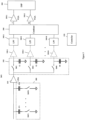
- FIG. 2 is a schematic diagram of another embodiment of a receiver circuit 200.
- Receiver circuit 200 includes low noise amplifier (LNA) 210, low-pass filter (LPF) 280, mixer 220, optional buffer 230, low-pass filter (LPF) 240, variable gain amplifier (VGA) 250, analog-to-digital converter (ADC) 260, and controller 270.
- LNA low noise amplifier
- LPF low-pass filter
- mixer 220 optional buffer 230
- LPF low-pass filter
- VGA variable gain amplifier
- ADC analog-to-digital converter
- controller 270 controller 270.
- Low noise amplifier 210 is configured to receive a high-frequency carrier signal modulated with a low frequency information signal as filtered by filter 280.
- the filtering of filter 280 is sufficient, that a SAW filter (or other similar) filter is not used to filter the high-frequency carrier signal prior to its being received by receiver 200.
- low noise amplifier 210 includes a matching network, as understood by those of skill in the art.
- the high-frequency carrier signal is an output of a matching network, as understood by one of skill in the art.
- the received signal also includes a blocker signal, such as a high power signal also modulating the high-frequency carrier signal near the frequency of the information signal.
- Low noise amplifier 210 may be any low noise amplifier or amplifier, as understood by those of skill in the art.
- filter 280 includes capacitor C2 and switch SW2. As understood by those of skill in the art, the connection relationship between capacitor C2 and switch SW2 may be reversed, such that switch SW2 is connected to LNA 210 and capacitor C2 is connected to ground. In some embodiments, filter 280 may be a multiphase filter, such as multiphase filter 380 discussed below.
- mixer 220 In response to the output from the low noise amplifier 210 and low-pass filter 280, and in response to control signals from controller 270, mixer 220 down converts the signal from the low noise amplifier 210 and low-pass filter 280.
- the resulting initial baseband signal includes information of the low frequency information signal and of the blocker signal.
- the baseband signal may then be processed by optional buffer 230. Because of the blocker signal, signals at the optional buffer 230 may exceed an input or output range limit, such that signals at the input, the output, or internal to the optional buffer 230 experience clipping. Not being part of the present invention, using techniques known to those of skill in the art, the clipping may be detected, and communicated to controller 270. In response to the detected clipping, controller 270 may generate control signals for optional buffer 230 to attenuate the baseband signal such that the signal range limit is no longer exceeded, and the clipping stops. Additionally or alternatively, in response to the detected clipping, controller 270 may generate control signals for low-pass filter 280 which cause low-pass filter 280 to attenuate the baseband signal such that the signal range limit is no longer exceeded, and the clipping stops.
- the optional buffer 230 does not detect whether the baseband signal exceeds a signal range limit.
- the baseband signal is then processed by the low-pass filter 240. Because of the blocker signal, signals at the low-pass filter 240 may exceed an input or output range limit, such that signals at the input, the output, or internal to the low-pass filter 240 experience clipping. Not being part of the present invention, using techniques known to those of skill in the art, the clipping may be detected, and communicated to controller 270. In response to the detected clipping, controller 270 may generate control signals for low-pass filter 240 to attenuate the baseband signal such that the signal range limit is no longer exceeded, and the clipping stops.
- controller 270 may generate control signals for optional buffer 230 to attenuate the baseband signal such that the signal range limit is no longer exceeded, and the clipping stops. Additionally or alternatively, in response to the detected clipping, controller 270 may generate control signals for low-pass filter 280 which cause low-pass filter 280 to attenuate the baseband signal such that the signal range limit is no longer exceeded, and the clipping stops.
- the low-pass filter 240 does not detect whether the baseband signal exceeds a signal range limit.
- the baseband signal is then processed by the variable gain amplifier 250. Because of the blocker signal, signals at the variable gain amplifier 250 exceed an input or output range limit, such that signals at the input, the output, or internal to the variable gain amplifier 250 experience clipping. Using techniques known to those of skill in the art, the clipping is detected, and communicated to controller 270. In response to the detected clipping, controller 270 generates control signals for low-pass filter 280 which cause low-pass filter 280 to attenuate the baseband signal such that the signal range limit is no longer exceeded, and the clipping stops.
- variable gain amplifier 250 does not detect whether the baseband signal exceeds a signal range limit.
- the baseband signal is then processed by the analog-to-digital converter 260. Because of the blocker signal, signals at the analog-to-digital converter 260 exceed an input or output range limit, such that signals at the input, the output, or internal to the analog-to-digital converter 260 experience clipping. Using techniques known to those of skill in the art, the clipping is detected, and communicated to controller 270. In response to the detected clipping, controller 270 generates control signal for low-pass filter 280 which cause low-pass filter 280 to attenuate the baseband signal such that the signal range limit is no longer exceeded, and the clipping stops.
- the analog-to-digital converter 260 does not detect whether the baseband signal exceeds a signal range limit.
- control signals from controller 270 causes one or more gain elements to attenuate the blocker signal. Additionally or alternatively, as understood by those of skill in the art, the control signals from controller 270 may cause one or more filtering elements to filter the blocker signal by, for example, moving a pole of the one or more filtering elements.
- FIG. 3 is a schematic diagram of yet another embodiment of a receiver circuit 300.
- Receiver circuit 300 includes low noise amplifier (LNA) 310, multi-phase mixer 320, optional buffers 330-1, 330-2 ... 330-N, low-pass filters (LPF) 340-1, 340-2 ... 340-N, combiner 390, variable gain amplifiers (VGA) 350-1 and 350-2, digital signal processor (DSP) 360, controller 370, and multiphase filter 380.
- LNA low noise amplifier
- LPF low-pass filters
- VGA variable gain amplifiers
- DSP digital signal processor
- Low noise amplifier 310 is configured to receive a high-frequency carrier signal modulated with a low frequency information signal as filtered by filter 380.
- the filtering of filter 380 is sufficient, that a SAW filter (or other similar) filter is not used to filter the high-frequency carrier signal prior to its being received by receiver 300.
- low noise amplifier 310 includes a matching network, as understood by those of skill in the art.
- the high-frequency carrier signal is an output of a matching network, as understood by one of skill in the art.
- filter 380 includes capacitors CF1 - CFN and switches SWF1-SWFN. As understood by those of skill in the art, the connection relationship between capacitors CF1 - CFN and switches SWF1-SWFN such that the capacitors CF1 - CFN may be connected to ground and switches SWF1-SWFN may be connected to LNA 310. In some embodiments, filter 380 may be a single phase filter, such as single phase filter 280 discussed above.
- the high-frequency carrier signal may also include a blocker signal, such as a high power signal also modulating the high-frequency carrier signal near the frequency of the information signal.
- Low noise amplifier 310 may be any low noise amplifier or amplifier, as understood by those of skill in the art.
- multi-phase mixer 320 In response to the output from the low noise amplifier 310, and in response to control signals from controller 370, multi-phase mixer 320 down converts the signal from the low noise amplifier 310.
- the resulting initial baseband signals include information of the low frequency information signal and of the blocker signal.
- the baseband signals may then be processed by optional buffers 330-1, 330-2 ... 330-N, which buffer the signals, as understood by those of ordinary skill in the art. Because of the blocker signal, signals at the optional buffers 330-1, 330-2 ... 330-N may exceed an input or output range limit, such that signals at the inputs, the outputs, or internal to the optional buffers 330-1, 330-2 ... 330-N experience clipping. Not being part of the present invention, using techniques known to those of skill in the art, the clipping may be detected, and communicated to controller 370. In response to the detected clipping, controller 370 may generate control signals for optional buffers 330-1, 330-2 ...
- controller 370 may generate control signals for multi-phase mixer 320 which cause multi-phase mixer 320 to attenuate the baseband signals such that the signal range limit is no longer exceeded, and the clipping stops. Additionally or alternatively, in response to the detected clipping, controller 370 may generate control signals for low-pass filter 380 which cause low-pass filter 380 to attenuate the baseband signal such that the signal range limit is no longer exceeded, and the clipping stops.
- optional buffers 330-1, 330-2 ... 330-N do not detect whether the baseband signal exceeds a signal range limit.
- the baseband signals are then processed by the low-pass filters 340-1, 340-2 ... 340-N, which filter the signals, as understood by those of ordinary skill in the art. Because of the blocker signal, signals at the low-pass filters 340-1, 340-2 ... 340-N may exceed an input or output range limit, such that signals at the input, the output, or internal to the low-pass filters 340-1, 340-2 ... 340-N experience clipping. Not being part of the present invention, using techniques known to those of skill in the art, the clipping may be detected, and communicated to controller 370. In response to the detected clipping, controller 370 may generate control signals for low-pass filters 340-1, 340-2 ...
- controller 370 may generate control signals for optional buffers 330-1, 330-2 ... 330-N to attenuate the baseband signal such that the signal range limit is no longer exceeded, and the clipping stops. Additionally or alternatively, in response to the detected clipping, controller 370 may generate control signals for multi-phase mixer 320 which cause multi-phase mixer 320 to attenuate the baseband signals such that the signal range limit is no longer exceeded, and the clipping stops. Additionally or alternatively, in response to the detected clipping, controller 370 may generate control signals for low-pass filter 380 which cause low-pass filter 380 to attenuate the baseband signal such that the signal range limit is no longer exceeded, and the clipping stops.
- the low-pass filters 340-1, 340-2 ... 340-N do not detect whether the baseband signal exceeds a signal range limit.
- the baseband signals are then processed by the combiner 390, which combines the signals to generate baseband I and Q signals, using techniques such as weighted harmonic rejection, as understood by those of ordinary skill in the art. Other combining techniques may be used. Because of the blocker signal, signals at the combiner 390 may exceed an input or output range limit, such that signals at the input, the output, or internal to the combiner 390 experience clipping. Not being part of the present invention, using techniques known to those of skill in the art, the clipping may be detected, and communicated to controller 370. In response to the detected clipping, controller 370 may generate control signals for combiner 390 to attenuate the baseband signal such that the signal range limit is no longer exceeded, and the clipping stops.
- controller 370 may generate control signals for combiner 390 to attenuate the baseband signal such that the signal range limit is no longer exceeded, and the clipping stops.
- controller 370 may generate control signals for low-pass filters 340-1, 340-2 ... 340-N to attenuate the baseband signal such that the signal range limit is no longer exceeded, and the clipping stops. Additionally or alternatively, in response to the detected clipping, controller 370 may generate control signals for optional buffers 330-1, 330-2 ... 330-N to attenuate the baseband signal such that the signal range limit is no longer exceeded, and the clipping stops. Additionally or alternatively, in response to the detected clipping, controller 370 may generate control signals for multi-phase mixer 320 which cause multi-phase mixer 320 to attenuate the baseband signals such that the signal range limit is no longer exceeded, and the clipping stops. Additionally or alternatively, in response to the detected clipping, controller 370 may generate control signals for low-pass filter 380 which cause low-pass filter 380 to attenuate the high-frequency carrier signal such that the signal range limit is no longer exceeded, and the clipping stops.
- low-pass filters 340-1, 340-2 ... 340-N may be included in combiner 390, such that a low-pass filter/combiner circuit receives baseband signals from either the multi-phase mixer 320 or the optional buffers 330-1, 330-2 ... 330-N, and both filters the baseband signals, and generates corresponding I and Q signals.
- the baseband I and Q signals are then processed by the variable gain amplifiers 350-1 and 350-2. Because of the blocker signal, signals at the variable gain amplifiers 350-1 and 350-2 may exceed an input or output range limit, such that signals at the input, the output, or internal to the variable gain amplifiers 350-1 and 350-2 experience clipping. Using techniques known to those of skill in the art, the clipping may be detected, and communicated to controller 370. In response to the detected clipping, controller 370 may generate control signals for variable gain amplifiers 350-1 and 350-2 to attenuate the baseband signal such that the signal range limit is no longer exceeded, and the clipping stops.
- controller 370 may generate control signals for combiner 390 to attenuate the baseband signal such that the signal range limit is no longer exceeded, and the clipping stops. Additionally or alternatively, in response to the detected clipping, controller 370 may generate control signals for low-pass filters 340-1, 340-2 ... 340-N to attenuate the baseband signal such that the signal range limit is no longer exceeded, and the clipping stops. Additionally or alternatively, in response to the detected clipping, controller 370 may generate control signals for optional buffers 330-1, 330-2 ... 330-N to attenuate the baseband signal such that the signal range limit is no longer exceeded, and the clipping stops.
- controller 370 may generate control signals for multi-phase mixer 320 which cause multi-phase mixer 320 to attenuate the baseband signals such that the signal range limit is no longer exceeded, and the clipping stops. Additionally or alternatively, in response to the detected clipping, controller 370 may generate control signals for low-pass filter 380 which cause low-pass filter 380 to attenuate the baseband signal such that the signal range limit is no longer exceeded, and the clipping stops.
- variable gain amplifiers 350-1 and 350-2 do not detect whether the baseband signal exceeds a signal range limit.
- the baseband signals are then processed by the digital signal processor 360. Because of the blocker signal, signals at the digital signal processor 360 may exceed an input or output range limit, such that signals at the input, the output, or internal to the digital signal processor 360 experience clipping. Using techniques known to those of skill in the art, the clipping may be detected, and communicated to controller 370. In response to the detected clipping, controller 370 may generate control signals for digital signal processor 360 to attenuate the baseband signal such that the signal range limit is no longer exceeded, and the clipping stops. Additionally or alternatively, in response to the detected clipping, controller 370 may generate control signals for variable gain amplifiers 350-1 and 350-2 to attenuate the baseband signal such that the signal range limit is no longer exceeded, and the clipping stops.
- controller 370 may generate control signals for low-pass filters 340-1, 340-2 ... 340-N to attenuate the baseband signal such that the signal range limit is no longer exceeded, and the clipping stops. Additionally or alternatively, in response to the detected clipping, controller 370 may generate control signals for optional buffers 330-1, 330-2 ... 330-N to attenuate the baseband signal such that the signal range limit is no longer exceeded, and the clipping stops. Additionally or alternatively, in response to the detected clipping, controller 370 may generate control signals for multi-phase mixer 320 which cause multi-phase mixer 320 to attenuate the baseband signals such that the signal range limit is no longer exceeded, and the clipping stops. Additionally or alternatively, in response to the detected clipping, controller 370 may generate control signals for low-pass filter 380 which cause low-pass filter 380 to attenuate the baseband signal such that the signal range limit is no longer exceeded, and the clipping stops.
- the digital signal processor 360 does not detect whether the baseband signal exceeds a signal range limit.
- control signals from controller 370 may cause one or more gain elements to attenuate the blocker signal. Additionally or alternatively, as understood by those of skill in the art, the control signals from controller 370 may cause one or more filtering elements to filter the blocker signal by, for example, moving a pole of the one or more filtering elements.
Landscapes
- Engineering & Computer Science (AREA)
- Computer Networks & Wireless Communication (AREA)
- Signal Processing (AREA)
- Power Engineering (AREA)
- Circuits Of Receivers In General (AREA)
- Amplifiers (AREA)
Claims (6)
- Empfängerschaltung (200), die Folgendes umfasst:einen Verstärker (210), der konfiguriert ist, basierend auf einem empfangenen Signal ein RF-Signal zu erzeugen, wobei das RF-Signal ein Informationssignal und ein Blockierersignal, die eine RF-Trägerfrequenz modulieren, umfasst;einen Einphasenmischer (220), der mit dem Verstärker (210) verbunden ist, wobei der Einphasenmischer (220) konfiguriert ist, das RF-Signal zu empfangen und das RF-Signal in ein Basisbandsignal abwärts umzusetzen, wobei das Basisbandsignal das Informationssignal und das Blockierersignal, die eine Basisbandsignalträgerfrequenz modulieren, umfasst, und wobei die Basisbandträgerfrequenz kleiner ist als die RF-Trägerfrequenz;ein RF-Filter (280), das mit dem Verstärker (210) verbunden ist, wobei das RF-Filter (280) konfiguriert ist, das Blockierersignal als Antwort auf ein Steuersignal, das von einer Steuereinrichtung (270) erzeugt wird, zu dämpfen;wobei die Empfängerschaltung (200) ferner einen Verstärker (250) mit variabler Verstärkung umfasst, der konfiguriert ist, das Basisband zu bearbeiten, wobei die Steuereinrichtung (270) konfiguriert ist, als Antwort auf das Eingangs- oder das Ausgangssignal an dem Verstärker (250) mit variabler Verstärkung, das eine Eingangs- oder Ausgangsbereichsgrenze des Verstärkers (250) mit variabler Verstärkung überschreitet, das Steuersignal für das RF-Filter (280) zu erzeugen, wobei das RF-Filter (280) konfiguriert ist, als Antwort auf die Steuersignale das Blockierersignal zu dämpfen; oderwobei die Empfängerschaltung (200) einen Analog/DigitalUmsetzer (260) umfasst, der konfiguriert ist, das Basisbandsignal zu bearbeiten, und die Steuereinrichtung (270) konfiguriert ist, als Antwort auf das Eingangs- oder das Ausgangssignal an dem Analog/Digital-Umsetzer (260), das eine Eingangs- oder Ausgangsbereichsgrenze des Analog/Digital-Umsetzers (260) überschreitet, das Steuersignal für das RF-Filter (280) zu erzeugen, wobei das RF-Filter (280) konfiguriert ist, als Antwort auf die Steuersignale das Blockierersignal zu dämpfen.
- Empfängerschaltung (200) nach Anspruch 1, wobei das RF-Filter (280) einen Kondensator (C2) umfasst, der einen Anschluss aufweist, der mit einem Eingang des Verstärkers (210) verbunden oder selektiv verbunden ist und der konfiguriert ist, das empfangene Signal zu empfangen.
- Empfängerschaltung (200) nach Anspruch 2, wobei das RF-Filter (280) einen Schalter (SW2) umfasst, der mit Masse oder dem Verstärker (210) verbunden ist.
- Verfahren zum Betreiben einer Empfängerschaltung (200), wobei die Empfängerschaltung Folgendes umfasst:einen Verstärker (210); undein RF-Filter (280), das mit dem Verstärker (210) verbunden ist,einen Einphasenmischer (220), der mit dem Verstärker (210) verbunden ist,wobei das Verfahren Folgendes umfasst:mit dem Verstärker (210) Erzeugen eines RF-Signals basierend auf einem empfangenen Signal, wobei das RF-Signal ein Informationssignal und ein Blockierersignal, die eine RF-Trägerfrequenz modulieren, umfasst;mit dem Einphasenmischer (220) Empfangen des RF-Signals und Abwärtsumsetzen des RF-Signals in ein Basisbandsignal, wobei das Basisbandsignal das Informationssignal und das Blockierersignal, die eine Basisbandträgerfrequenz modulieren, umfasst und wobei die Basisbandträgerfrequenz kleiner ist als die RF-Trägerfrequenz;mit dem RF-Filter (280) Dämpfen des Blockierersignals als Antwort auf ein Steuersignal, das von einer Steuereinrichtung (270) erzeugt wird;wobei die Empfängerschaltung (200) ferner einen Verstärker (250) mit variabler Verstärkung oder einen Analog/DigitalUmsetzer (260) umfasst und wobei das Verfahren ferner Folgendes umfasst:mit dem Verstärker (250) mit variabler Verstärkung, Bearbeiten des Basisbandsignals, mit der Steuereinrichtung (270) Erzeugen des Steuersignals für das RF-Filter (280) als Antwort auf das Eingangs- oder Ausgangssignal an dem Verstärker (250) mit variabler Verstärkung, das eine Eingangs- oder Ausgangsbereichsgrenze des Verstärkers (250) mit variabler Verstärkung überschreitet, und mit dem RF-Filter (280) als Antwort auf die Steuersignale Dämpfen des Blockierersignals; odermit dem Analog/Digital-Umsetzer (260) Bearbeiten des Basisbandsignals, mit der Steuereinrichtung (270) Erzeugen des Steuersignals für das RF-Filter (280) als Antwort auf das Eingangs- oder Ausgangssignal an dem Analog/DigitalUmsetzer (260), das eine Eingangs- oder Ausgangsbereichsgrenze des Analog/Digital-Umsetzers (260) überschreitet, und mit dem RF-Filter (280) als Antwort auf die Steuersignale Dämpfen des Blockierersignals.
- Verfahren nach Anspruch 4, wobei das RF-Filter einen Kondensator (C2) umfasst, der einen Anschluss aufweist, der mit einem Eingang des Verstärkers (210) verbunden oder selektiv verbunden ist und der konfiguriert ist, das empfangene Signal zu empfangen.
- Verfahren nach Anspruch 5, wobei das RF-Filter (280) einen Schalter (SW2) umfasst, der mit Masse oder dem Verstärker (210) verbunden ist.
Applications Claiming Priority (2)
| Application Number | Priority Date | Filing Date | Title |
|---|---|---|---|
| US16/749,996 US10873486B1 (en) | 2020-01-23 | 2020-01-23 | Receiver circuits with blocker attenuating RF filter |
| PCT/CN2021/071598 WO2021147743A1 (en) | 2020-01-23 | 2021-01-13 | Receiver circuits with blocker attenuating rf filter |
Publications (3)
| Publication Number | Publication Date |
|---|---|
| EP4005097A1 EP4005097A1 (de) | 2022-06-01 |
| EP4005097A4 EP4005097A4 (de) | 2022-10-12 |
| EP4005097B1 true EP4005097B1 (de) | 2024-08-21 |
Family
ID=73823621
Family Applications (1)
| Application Number | Title | Priority Date | Filing Date |
|---|---|---|---|
| EP21743857.1A Active EP4005097B1 (de) | 2020-01-23 | 2021-01-13 | Empfängerschaltungen mit einem blockerdämpfenden rf-filter |
Country Status (4)
| Country | Link |
|---|---|
| US (2) | US10873486B1 (de) |
| EP (1) | EP4005097B1 (de) |
| CN (1) | CN114342270B (de) |
| WO (1) | WO2021147743A1 (de) |
Families Citing this family (9)
| Publication number | Priority date | Publication date | Assignee | Title |
|---|---|---|---|---|
| US11387857B2 (en) * | 2019-12-06 | 2022-07-12 | Silicon Laboratories Inc. | Dynamically reconfigurable frequency selective attenuator for radio frequency receiver front end |
| US11463064B2 (en) | 2019-12-06 | 2022-10-04 | Silicon Laboratories Inc. | Frequency selective attenuator for optimized radio frequency coexistence |
| US11177988B2 (en) * | 2020-01-23 | 2021-11-16 | Shenzhen GOODIX Technology Co., Ltd. | Receiver circuits with blocker attenuating mixer |
| US10873486B1 (en) | 2020-01-23 | 2020-12-22 | Goodix Technology Inc. | Receiver circuits with blocker attenuating RF filter |
| US11356136B2 (en) * | 2020-09-08 | 2022-06-07 | Shenzhen GOODIX Technology Co., Ltd. | Harmonic rejection in multiphase signals |
| US11750166B2 (en) | 2021-01-13 | 2023-09-05 | Marvell Asia Pte. Ltd. | Method and device for high bandwidth receiver for high baud-rate communications |
| US11309904B1 (en) | 2021-02-24 | 2022-04-19 | Marvell Asia Pte Ltd. | Method and device for synchronization of large-scale systems with multiple time interleaving sub-systems |
| US11456760B1 (en) * | 2021-03-05 | 2022-09-27 | Motorola Solutions, Inc. | Linearizing narrowband carriers with low resolution predistorters |
| KR20240048103A (ko) * | 2022-10-06 | 2024-04-15 | 주식회사 디비하이텍 | 수신기 입력부의 블록커 신호 제거장치 및 방법 |
Citations (1)
| Publication number | Priority date | Publication date | Assignee | Title |
|---|---|---|---|---|
| US20130115904A1 (en) * | 2010-07-13 | 2013-05-09 | St-Ericsson Sa | Synchronizing and Detecting Interference in Wireless Receiver |
Family Cites Families (19)
| Publication number | Priority date | Publication date | Assignee | Title |
|---|---|---|---|---|
| KR100251560B1 (ko) | 1996-10-29 | 2000-04-15 | 윤종용 | 부호분할 다중 접속방식 단말기의 외부 간섭신호 제거장치 |
| JPH11136154A (ja) | 1997-10-31 | 1999-05-21 | Sony Corp | 受信装置 |
| GB9807052D0 (en) | 1998-04-02 | 1998-06-03 | Philips Consumer Communication | Communications device |
| EP1710920A1 (de) * | 2005-04-06 | 2006-10-11 | Telefonaktiebolaget LM Ericsson (publ) | Empfang von modulierten Funksignalen |
| JP5075605B2 (ja) * | 2007-12-13 | 2012-11-21 | 株式会社東芝 | 受信装置 |
| US7773545B2 (en) | 2008-02-27 | 2010-08-10 | Mediatek Inc. | Full division duplex system and a leakage cancellation method |
| US8145172B2 (en) * | 2008-11-25 | 2012-03-27 | Silicon Laboratories Inc. | Low-cost receiver using tracking filter |
| US8606209B2 (en) | 2009-06-24 | 2013-12-10 | Intel Corporation | Apparatus and methods for efficient implementation of tuners |
| WO2011066474A1 (en) | 2009-11-24 | 2011-06-03 | Maxlinear, Inc. | Analog front end circuit for cable and wireless systems |
| US8655299B2 (en) * | 2010-06-03 | 2014-02-18 | Broadcom Corporation | Saw-less receiver with RF frequency translated BPF |
| US8761710B2 (en) * | 2010-06-03 | 2014-06-24 | Broadcom Corporation | Portable computing device with a saw-less transceiver |
| US8725085B2 (en) * | 2010-06-03 | 2014-05-13 | Broadcom Corporation | RF front-end module |
| US9154166B2 (en) * | 2010-06-03 | 2015-10-06 | Broadcom Corporation | Front-end module network |
| US8693595B2 (en) * | 2011-05-10 | 2014-04-08 | Issc Technologies Corp. | Adaptive wireless communication receiver |
| CN102231906B (zh) * | 2011-06-22 | 2017-04-12 | 中兴通讯股份有限公司 | 一种增益控制方法及射频拉远单元 |
| EP2624463B1 (de) | 2012-02-03 | 2015-04-15 | Telefonaktiebolaget L M Ericsson (PUBL) | Abwärtskonvertierungsschaltung mit Interferenzerkennung |
| US10027355B2 (en) | 2016-01-19 | 2018-07-17 | Analog Devices Global | Blocker detection based automatic gain control |
| US9929769B1 (en) | 2017-01-20 | 2018-03-27 | Resonant Inc. | Communications receiver using multi-band transmit blocking filters |
| US10873486B1 (en) | 2020-01-23 | 2020-12-22 | Goodix Technology Inc. | Receiver circuits with blocker attenuating RF filter |
-
2020
- 2020-01-23 US US16/749,996 patent/US10873486B1/en active Active
- 2020-11-16 US US17/098,456 patent/US11546192B2/en active Active
-
2021
- 2021-01-13 EP EP21743857.1A patent/EP4005097B1/de active Active
- 2021-01-13 WO PCT/CN2021/071598 patent/WO2021147743A1/en not_active Ceased
- 2021-01-13 CN CN202180005000.9A patent/CN114342270B/zh active Active
Patent Citations (1)
| Publication number | Priority date | Publication date | Assignee | Title |
|---|---|---|---|---|
| US20130115904A1 (en) * | 2010-07-13 | 2013-05-09 | St-Ericsson Sa | Synchronizing and Detecting Interference in Wireless Receiver |
Also Published As
| Publication number | Publication date |
|---|---|
| US10873486B1 (en) | 2020-12-22 |
| US20210234737A1 (en) | 2021-07-29 |
| CN114342270A (zh) | 2022-04-12 |
| CN114342270B (zh) | 2023-09-05 |
| US11546192B2 (en) | 2023-01-03 |
| EP4005097A4 (de) | 2022-10-12 |
| EP4005097A1 (de) | 2022-06-01 |
| WO2021147743A1 (en) | 2021-07-29 |
Similar Documents
| Publication | Publication Date | Title |
|---|---|---|
| EP4005097B1 (de) | Empfängerschaltungen mit einem blockerdämpfenden rf-filter | |
| US11177988B2 (en) | Receiver circuits with blocker attenuating mixer | |
| US7804922B2 (en) | System and method for adjacent channel power detection and dynamic bandwidth filter control | |
| US5678213A (en) | Radio receiver for processing a multi-carrier signal with a large dynamic range | |
| US20120189040A1 (en) | Multi-mode receiver | |
| US8624654B2 (en) | Automatic step variable attenuator and radio communication device | |
| JP2005151011A (ja) | 高周波信号受信装置および半導体集積回路 | |
| WO2009024085A1 (fr) | Procédé antibrouillage pour récepteur, récepteur antibrouillage et dispositif antibrouillage | |
| KR20070100843A (ko) | Rf 수신기에서의 전달―임피던스 필터링 | |
| CN111245457B (zh) | 一种兼容宽窄带信号的接收机直流处理方法 | |
| US4761828A (en) | Radio receiver | |
| US9859857B2 (en) | DC offset cancellation circuit | |
| EP1710920A1 (de) | Empfang von modulierten Funksignalen | |
| US20060009186A1 (en) | Receiver front-end filtering using low pass filtering and equalization | |
| JP3746209B2 (ja) | 無線送受信機 | |
| WO2013147581A1 (en) | Method and apparatus for reducing fm audio artifacts in a receiver | |
| US20210351800A1 (en) | Radio-frequency module and communication apparatus | |
| JP2001136447A (ja) | デジタルテレビジョン受信用チューナ | |
| JP4755666B2 (ja) | 無線通信モジュール | |
| JPH07326980A (ja) | 移動通信用受信機 | |
| WO2006137007A1 (en) | Transmitter in wireless communication system | |
| JP2010147975A (ja) | 高周波受信装置 | |
| KR20030006574A (ko) | Dc 오프셋 제거 회로 | |
| JP2010004286A (ja) | 高周波受信装置、放送受信機、および高周波受信装置の利得制御方法 | |
| JP2002031657A (ja) | 受信電界強度検出信号の生成回路とその生成回路を具備する移動体通信装置。 |
Legal Events
| Date | Code | Title | Description |
|---|---|---|---|
| STAA | Information on the status of an ep patent application or granted ep patent |
Free format text: STATUS: THE INTERNATIONAL PUBLICATION HAS BEEN MADE |
|
| PUAI | Public reference made under article 153(3) epc to a published international application that has entered the european phase |
Free format text: ORIGINAL CODE: 0009012 |
|
| STAA | Information on the status of an ep patent application or granted ep patent |
Free format text: STATUS: REQUEST FOR EXAMINATION WAS MADE |
|
| 17P | Request for examination filed |
Effective date: 20220223 |
|
| AK | Designated contracting states |
Kind code of ref document: A1 Designated state(s): AL AT BE BG CH CY CZ DE DK EE ES FI FR GB GR HR HU IE IS IT LI LT LU LV MC MK MT NL NO PL PT RO RS SE SI SK SM TR |
|
| A4 | Supplementary search report drawn up and despatched |
Effective date: 20220912 |
|
| RIC1 | Information provided on ipc code assigned before grant |
Ipc: H04L 27/14 20060101ALI20220906BHEP Ipc: H03F 3/189 20060101ALI20220906BHEP Ipc: H04B 1/12 20060101ALI20220906BHEP Ipc: H04B 1/10 20060101AFI20220906BHEP |
|
| DAV | Request for validation of the european patent (deleted) | ||
| DAX | Request for extension of the european patent (deleted) | ||
| STAA | Information on the status of an ep patent application or granted ep patent |
Free format text: STATUS: EXAMINATION IS IN PROGRESS |
|
| 17Q | First examination report despatched |
Effective date: 20230606 |
|
| GRAP | Despatch of communication of intention to grant a patent |
Free format text: ORIGINAL CODE: EPIDOSNIGR1 |
|
| STAA | Information on the status of an ep patent application or granted ep patent |
Free format text: STATUS: GRANT OF PATENT IS INTENDED |
|
| GRAS | Grant fee paid |
Free format text: ORIGINAL CODE: EPIDOSNIGR3 |
|
| INTG | Intention to grant announced |
Effective date: 20240617 |
|
| GRAA | (expected) grant |
Free format text: ORIGINAL CODE: 0009210 |
|
| STAA | Information on the status of an ep patent application or granted ep patent |
Free format text: STATUS: THE PATENT HAS BEEN GRANTED |
|
| AK | Designated contracting states |
Kind code of ref document: B1 Designated state(s): AL AT BE BG CH CY CZ DE DK EE ES FI FR GB GR HR HU IE IS IT LI LT LU LV MC MK MT NL NO PL PT RO RS SE SI SK SM TR |
|
| REG | Reference to a national code |
Ref country code: GB Ref legal event code: FG4D |
|
| REG | Reference to a national code |
Ref country code: CH Ref legal event code: EP |
|
| REG | Reference to a national code |
Ref country code: IE Ref legal event code: FG4D |
|
| REG | Reference to a national code |
Ref country code: DE Ref legal event code: R096 Ref document number: 602021017581 Country of ref document: DE |
|
| REG | Reference to a national code |
Ref country code: LT Ref legal event code: MG9D |
|
| REG | Reference to a national code |
Ref country code: NL Ref legal event code: MP Effective date: 20240821 |
|
| PG25 | Lapsed in a contracting state [announced via postgrant information from national office to epo] |
Ref country code: NO Free format text: LAPSE BECAUSE OF FAILURE TO SUBMIT A TRANSLATION OF THE DESCRIPTION OR TO PAY THE FEE WITHIN THE PRESCRIBED TIME-LIMIT Effective date: 20241121 |
|
| REG | Reference to a national code |
Ref country code: AT Ref legal event code: MK05 Ref document number: 1716531 Country of ref document: AT Kind code of ref document: T Effective date: 20240821 |
|
| PG25 | Lapsed in a contracting state [announced via postgrant information from national office to epo] |
Ref country code: NL Free format text: LAPSE BECAUSE OF FAILURE TO SUBMIT A TRANSLATION OF THE DESCRIPTION OR TO PAY THE FEE WITHIN THE PRESCRIBED TIME-LIMIT Effective date: 20240821 Ref country code: FI Free format text: LAPSE BECAUSE OF FAILURE TO SUBMIT A TRANSLATION OF THE DESCRIPTION OR TO PAY THE FEE WITHIN THE PRESCRIBED TIME-LIMIT Effective date: 20240821 Ref country code: PL Free format text: LAPSE BECAUSE OF FAILURE TO SUBMIT A TRANSLATION OF THE DESCRIPTION OR TO PAY THE FEE WITHIN THE PRESCRIBED TIME-LIMIT Effective date: 20240821 Ref country code: PT Free format text: LAPSE BECAUSE OF FAILURE TO SUBMIT A TRANSLATION OF THE DESCRIPTION OR TO PAY THE FEE WITHIN THE PRESCRIBED TIME-LIMIT Effective date: 20241223 Ref country code: GR Free format text: LAPSE BECAUSE OF FAILURE TO SUBMIT A TRANSLATION OF THE DESCRIPTION OR TO PAY THE FEE WITHIN THE PRESCRIBED TIME-LIMIT Effective date: 20241122 |
|
| PG25 | Lapsed in a contracting state [announced via postgrant information from national office to epo] |
Ref country code: BG Free format text: LAPSE BECAUSE OF FAILURE TO SUBMIT A TRANSLATION OF THE DESCRIPTION OR TO PAY THE FEE WITHIN THE PRESCRIBED TIME-LIMIT Effective date: 20240821 |
|
| PG25 | Lapsed in a contracting state [announced via postgrant information from national office to epo] |
Ref country code: LV Free format text: LAPSE BECAUSE OF FAILURE TO SUBMIT A TRANSLATION OF THE DESCRIPTION OR TO PAY THE FEE WITHIN THE PRESCRIBED TIME-LIMIT Effective date: 20240821 |
|
| PG25 | Lapsed in a contracting state [announced via postgrant information from national office to epo] |
Ref country code: IS Free format text: LAPSE BECAUSE OF FAILURE TO SUBMIT A TRANSLATION OF THE DESCRIPTION OR TO PAY THE FEE WITHIN THE PRESCRIBED TIME-LIMIT Effective date: 20241221 Ref country code: AT Free format text: LAPSE BECAUSE OF FAILURE TO SUBMIT A TRANSLATION OF THE DESCRIPTION OR TO PAY THE FEE WITHIN THE PRESCRIBED TIME-LIMIT Effective date: 20240821 |
|
| PG25 | Lapsed in a contracting state [announced via postgrant information from national office to epo] |
Ref country code: HR Free format text: LAPSE BECAUSE OF FAILURE TO SUBMIT A TRANSLATION OF THE DESCRIPTION OR TO PAY THE FEE WITHIN THE PRESCRIBED TIME-LIMIT Effective date: 20240821 |
|
| PG25 | Lapsed in a contracting state [announced via postgrant information from national office to epo] |
Ref country code: ES Free format text: LAPSE BECAUSE OF FAILURE TO SUBMIT A TRANSLATION OF THE DESCRIPTION OR TO PAY THE FEE WITHIN THE PRESCRIBED TIME-LIMIT Effective date: 20240821 Ref country code: RS Free format text: LAPSE BECAUSE OF FAILURE TO SUBMIT A TRANSLATION OF THE DESCRIPTION OR TO PAY THE FEE WITHIN THE PRESCRIBED TIME-LIMIT Effective date: 20241121 |
|
| PG25 | Lapsed in a contracting state [announced via postgrant information from national office to epo] |
Ref country code: RS Free format text: LAPSE BECAUSE OF FAILURE TO SUBMIT A TRANSLATION OF THE DESCRIPTION OR TO PAY THE FEE WITHIN THE PRESCRIBED TIME-LIMIT Effective date: 20241121 Ref country code: PT Free format text: LAPSE BECAUSE OF FAILURE TO SUBMIT A TRANSLATION OF THE DESCRIPTION OR TO PAY THE FEE WITHIN THE PRESCRIBED TIME-LIMIT Effective date: 20241223 Ref country code: PL Free format text: LAPSE BECAUSE OF FAILURE TO SUBMIT A TRANSLATION OF THE DESCRIPTION OR TO PAY THE FEE WITHIN THE PRESCRIBED TIME-LIMIT Effective date: 20240821 Ref country code: NO Free format text: LAPSE BECAUSE OF FAILURE TO SUBMIT A TRANSLATION OF THE DESCRIPTION OR TO PAY THE FEE WITHIN THE PRESCRIBED TIME-LIMIT Effective date: 20241121 Ref country code: NL Free format text: LAPSE BECAUSE OF FAILURE TO SUBMIT A TRANSLATION OF THE DESCRIPTION OR TO PAY THE FEE WITHIN THE PRESCRIBED TIME-LIMIT Effective date: 20240821 Ref country code: LV Free format text: LAPSE BECAUSE OF FAILURE TO SUBMIT A TRANSLATION OF THE DESCRIPTION OR TO PAY THE FEE WITHIN THE PRESCRIBED TIME-LIMIT Effective date: 20240821 Ref country code: IS Free format text: LAPSE BECAUSE OF FAILURE TO SUBMIT A TRANSLATION OF THE DESCRIPTION OR TO PAY THE FEE WITHIN THE PRESCRIBED TIME-LIMIT Effective date: 20241221 Ref country code: HR Free format text: LAPSE BECAUSE OF FAILURE TO SUBMIT A TRANSLATION OF THE DESCRIPTION OR TO PAY THE FEE WITHIN THE PRESCRIBED TIME-LIMIT Effective date: 20240821 Ref country code: GR Free format text: LAPSE BECAUSE OF FAILURE TO SUBMIT A TRANSLATION OF THE DESCRIPTION OR TO PAY THE FEE WITHIN THE PRESCRIBED TIME-LIMIT Effective date: 20241122 Ref country code: FI Free format text: LAPSE BECAUSE OF FAILURE TO SUBMIT A TRANSLATION OF THE DESCRIPTION OR TO PAY THE FEE WITHIN THE PRESCRIBED TIME-LIMIT Effective date: 20240821 Ref country code: ES Free format text: LAPSE BECAUSE OF FAILURE TO SUBMIT A TRANSLATION OF THE DESCRIPTION OR TO PAY THE FEE WITHIN THE PRESCRIBED TIME-LIMIT Effective date: 20240821 Ref country code: BG Free format text: LAPSE BECAUSE OF FAILURE TO SUBMIT A TRANSLATION OF THE DESCRIPTION OR TO PAY THE FEE WITHIN THE PRESCRIBED TIME-LIMIT Effective date: 20240821 Ref country code: AT Free format text: LAPSE BECAUSE OF FAILURE TO SUBMIT A TRANSLATION OF THE DESCRIPTION OR TO PAY THE FEE WITHIN THE PRESCRIBED TIME-LIMIT Effective date: 20240821 |
|
| PG25 | Lapsed in a contracting state [announced via postgrant information from national office to epo] |
Ref country code: RO Free format text: LAPSE BECAUSE OF FAILURE TO SUBMIT A TRANSLATION OF THE DESCRIPTION OR TO PAY THE FEE WITHIN THE PRESCRIBED TIME-LIMIT Effective date: 20240821 Ref country code: SM Free format text: LAPSE BECAUSE OF FAILURE TO SUBMIT A TRANSLATION OF THE DESCRIPTION OR TO PAY THE FEE WITHIN THE PRESCRIBED TIME-LIMIT Effective date: 20240821 Ref country code: DK Free format text: LAPSE BECAUSE OF FAILURE TO SUBMIT A TRANSLATION OF THE DESCRIPTION OR TO PAY THE FEE WITHIN THE PRESCRIBED TIME-LIMIT Effective date: 20240821 |
|
| PG25 | Lapsed in a contracting state [announced via postgrant information from national office to epo] |
Ref country code: EE Free format text: LAPSE BECAUSE OF FAILURE TO SUBMIT A TRANSLATION OF THE DESCRIPTION OR TO PAY THE FEE WITHIN THE PRESCRIBED TIME-LIMIT Effective date: 20240821 |
|
| PG25 | Lapsed in a contracting state [announced via postgrant information from national office to epo] |
Ref country code: CZ Free format text: LAPSE BECAUSE OF FAILURE TO SUBMIT A TRANSLATION OF THE DESCRIPTION OR TO PAY THE FEE WITHIN THE PRESCRIBED TIME-LIMIT Effective date: 20240821 |
|
| PG25 | Lapsed in a contracting state [announced via postgrant information from national office to epo] |
Ref country code: SK Free format text: LAPSE BECAUSE OF FAILURE TO SUBMIT A TRANSLATION OF THE DESCRIPTION OR TO PAY THE FEE WITHIN THE PRESCRIBED TIME-LIMIT Effective date: 20240821 Ref country code: IT Free format text: LAPSE BECAUSE OF FAILURE TO SUBMIT A TRANSLATION OF THE DESCRIPTION OR TO PAY THE FEE WITHIN THE PRESCRIBED TIME-LIMIT Effective date: 20240821 |
|
| REG | Reference to a national code |
Ref country code: DE Ref legal event code: R097 Ref document number: 602021017581 Country of ref document: DE |
|
| PLBE | No opposition filed within time limit |
Free format text: ORIGINAL CODE: 0009261 |
|
| STAA | Information on the status of an ep patent application or granted ep patent |
Free format text: STATUS: NO OPPOSITION FILED WITHIN TIME LIMIT |
|
| 26N | No opposition filed |
Effective date: 20250522 |
|
| REG | Reference to a national code |
Ref country code: DE Ref legal event code: R119 Ref document number: 602021017581 Country of ref document: DE |
|
| REG | Reference to a national code |
Ref country code: CH Ref legal event code: PL |
|
| PG25 | Lapsed in a contracting state [announced via postgrant information from national office to epo] |
Ref country code: SE Free format text: LAPSE BECAUSE OF FAILURE TO SUBMIT A TRANSLATION OF THE DESCRIPTION OR TO PAY THE FEE WITHIN THE PRESCRIBED TIME-LIMIT Effective date: 20240821 |
|
| PG25 | Lapsed in a contracting state [announced via postgrant information from national office to epo] |
Ref country code: MC Free format text: LAPSE BECAUSE OF FAILURE TO SUBMIT A TRANSLATION OF THE DESCRIPTION OR TO PAY THE FEE WITHIN THE PRESCRIBED TIME-LIMIT Effective date: 20240821 Ref country code: LU Free format text: LAPSE BECAUSE OF NON-PAYMENT OF DUE FEES Effective date: 20250113 |
|
| GBPC | Gb: european patent ceased through non-payment of renewal fee |
Effective date: 20250113 |
|
| PG25 | Lapsed in a contracting state [announced via postgrant information from national office to epo] |
Ref country code: DE Free format text: LAPSE BECAUSE OF NON-PAYMENT OF DUE FEES Effective date: 20250801 |
|
| PG25 | Lapsed in a contracting state [announced via postgrant information from national office to epo] |
Ref country code: BE Free format text: LAPSE BECAUSE OF NON-PAYMENT OF DUE FEES Effective date: 20250131 Ref country code: GB Free format text: LAPSE BECAUSE OF NON-PAYMENT OF DUE FEES Effective date: 20250113 |
|
| PG25 | Lapsed in a contracting state [announced via postgrant information from national office to epo] |
Ref country code: FR Free format text: LAPSE BECAUSE OF NON-PAYMENT OF DUE FEES Effective date: 20250131 |
|
| PG25 | Lapsed in a contracting state [announced via postgrant information from national office to epo] |
Ref country code: CH Free format text: LAPSE BECAUSE OF NON-PAYMENT OF DUE FEES Effective date: 20250131 |
|
| REG | Reference to a national code |
Ref country code: BE Ref legal event code: MM Effective date: 20250131 |
|
| PG25 | Lapsed in a contracting state [announced via postgrant information from national office to epo] |
Ref country code: IE Free format text: LAPSE BECAUSE OF NON-PAYMENT OF DUE FEES Effective date: 20250113 |