EP4005802A1 - Dispositif d'impression à jet d'encre, procédé permettant d'aligner un élément bipolaire et procédé permettant de fabriquer un dispositif d'affichage - Google Patents
Dispositif d'impression à jet d'encre, procédé permettant d'aligner un élément bipolaire et procédé permettant de fabriquer un dispositif d'affichage Download PDFInfo
- Publication number
- EP4005802A1 EP4005802A1 EP20843237.7A EP20843237A EP4005802A1 EP 4005802 A1 EP4005802 A1 EP 4005802A1 EP 20843237 A EP20843237 A EP 20843237A EP 4005802 A1 EP4005802 A1 EP 4005802A1
- Authority
- EP
- European Patent Office
- Prior art keywords
- electrode
- electric field
- ink
- disposed
- printing device
- Prior art date
- Legal status (The legal status is an assumption and is not a legal conclusion. Google has not performed a legal analysis and makes no representation as to the accuracy of the status listed.)
- Pending
Links
Images


Classifications
-
- B—PERFORMING OPERATIONS; TRANSPORTING
- B41—PRINTING; LINING MACHINES; TYPEWRITERS; STAMPS
- B41J—TYPEWRITERS; SELECTIVE PRINTING MECHANISMS, i.e. MECHANISMS PRINTING OTHERWISE THAN FROM A FORME; CORRECTION OF TYPOGRAPHICAL ERRORS
- B41J2/00—Typewriters or selective printing mechanisms characterised by the printing or marking process for which they are designed
- B41J2/005—Typewriters or selective printing mechanisms characterised by the printing or marking process for which they are designed characterised by bringing liquid or particles selectively into contact with a printing material
- B41J2/01—Ink jet
- B41J2/135—Nozzles
- B41J2/14—Structure thereof only for on-demand ink jet heads
- B41J2/14016—Structure of bubble jet print heads
- B41J2/14072—Electrical connections, e.g. details on electrodes, connecting the chip to the outside...
-
- H—ELECTRICITY
- H10—SEMICONDUCTOR DEVICES; ELECTRIC SOLID-STATE DEVICES NOT OTHERWISE PROVIDED FOR
- H10H—INORGANIC LIGHT-EMITTING SEMICONDUCTOR DEVICES HAVING POTENTIAL BARRIERS
- H10H20/00—Individual inorganic light-emitting semiconductor devices having potential barriers, e.g. light-emitting diodes [LED]
- H10H20/01—Manufacture or treatment
-
- B—PERFORMING OPERATIONS; TRANSPORTING
- B41—PRINTING; LINING MACHINES; TYPEWRITERS; STAMPS
- B41J—TYPEWRITERS; SELECTIVE PRINTING MECHANISMS, i.e. MECHANISMS PRINTING OTHERWISE THAN FROM A FORME; CORRECTION OF TYPOGRAPHICAL ERRORS
- B41J2/00—Typewriters or selective printing mechanisms characterised by the printing or marking process for which they are designed
- B41J2/005—Typewriters or selective printing mechanisms characterised by the printing or marking process for which they are designed characterised by bringing liquid or particles selectively into contact with a printing material
- B41J2/01—Ink jet
- B41J2/015—Ink jet characterised by the jet generation process
- B41J2/04—Ink jet characterised by the jet generation process generating single droplets or particles on demand
- B41J2/06—Ink jet characterised by the jet generation process generating single droplets or particles on demand by electric or magnetic field
-
- B—PERFORMING OPERATIONS; TRANSPORTING
- B41—PRINTING; LINING MACHINES; TYPEWRITERS; STAMPS
- B41J—TYPEWRITERS; SELECTIVE PRINTING MECHANISMS, i.e. MECHANISMS PRINTING OTHERWISE THAN FROM A FORME; CORRECTION OF TYPOGRAPHICAL ERRORS
- B41J2/00—Typewriters or selective printing mechanisms characterised by the printing or marking process for which they are designed
- B41J2/005—Typewriters or selective printing mechanisms characterised by the printing or marking process for which they are designed characterised by bringing liquid or particles selectively into contact with a printing material
- B41J2/01—Ink jet
- B41J2/07—Ink jet characterised by jet control
- B41J2/075—Ink jet characterised by jet control for many-valued deflection
- B41J2/08—Ink jet characterised by jet control for many-valued deflection charge-control type
- B41J2/085—Charge means, e.g. electrodes
-
- B—PERFORMING OPERATIONS; TRANSPORTING
- B41—PRINTING; LINING MACHINES; TYPEWRITERS; STAMPS
- B41J—TYPEWRITERS; SELECTIVE PRINTING MECHANISMS, i.e. MECHANISMS PRINTING OTHERWISE THAN FROM A FORME; CORRECTION OF TYPOGRAPHICAL ERRORS
- B41J2/00—Typewriters or selective printing mechanisms characterised by the printing or marking process for which they are designed
- B41J2/005—Typewriters or selective printing mechanisms characterised by the printing or marking process for which they are designed characterised by bringing liquid or particles selectively into contact with a printing material
- B41J2/01—Ink jet
- B41J2/07—Ink jet characterised by jet control
- B41J2/075—Ink jet characterised by jet control for many-valued deflection
- B41J2/095—Ink jet characterised by jet control for many-valued deflection electric field-control type
-
- B—PERFORMING OPERATIONS; TRANSPORTING
- B41—PRINTING; LINING MACHINES; TYPEWRITERS; STAMPS
- B41J—TYPEWRITERS; SELECTIVE PRINTING MECHANISMS, i.e. MECHANISMS PRINTING OTHERWISE THAN FROM A FORME; CORRECTION OF TYPOGRAPHICAL ERRORS
- B41J2/00—Typewriters or selective printing mechanisms characterised by the printing or marking process for which they are designed
- B41J2/005—Typewriters or selective printing mechanisms characterised by the printing or marking process for which they are designed characterised by bringing liquid or particles selectively into contact with a printing material
- B41J2/01—Ink jet
- B41J2/135—Nozzles
- B41J2/14—Structure thereof only for on-demand ink jet heads
- B41J2/1433—Structure of nozzle plates
-
- H—ELECTRICITY
- H10—SEMICONDUCTOR DEVICES; ELECTRIC SOLID-STATE DEVICES NOT OTHERWISE PROVIDED FOR
- H10H—INORGANIC LIGHT-EMITTING SEMICONDUCTOR DEVICES HAVING POTENTIAL BARRIERS
- H10H20/00—Individual inorganic light-emitting semiconductor devices having potential barriers, e.g. light-emitting diodes [LED]
- H10H20/80—Constructional details
- H10H20/81—Bodies
- H10H20/819—Bodies characterised by their shape, e.g. curved or truncated substrates
- H10H20/821—Bodies characterised by their shape, e.g. curved or truncated substrates of the light-emitting regions, e.g. non-planar junctions
-
- H—ELECTRICITY
- H10—SEMICONDUCTOR DEVICES; ELECTRIC SOLID-STATE DEVICES NOT OTHERWISE PROVIDED FOR
- H10H—INORGANIC LIGHT-EMITTING SEMICONDUCTOR DEVICES HAVING POTENTIAL BARRIERS
- H10H20/00—Individual inorganic light-emitting semiconductor devices having potential barriers, e.g. light-emitting diodes [LED]
- H10H20/80—Constructional details
- H10H20/84—Coatings, e.g. passivation layers or antireflective coatings
-
- H—ELECTRICITY
- H10—SEMICONDUCTOR DEVICES; ELECTRIC SOLID-STATE DEVICES NOT OTHERWISE PROVIDED FOR
- H10H—INORGANIC LIGHT-EMITTING SEMICONDUCTOR DEVICES HAVING POTENTIAL BARRIERS
- H10H29/00—Integrated devices, or assemblies of multiple devices, comprising at least one light-emitting semiconductor element covered by group H10H20/00
- H10H29/10—Integrated devices comprising at least one light-emitting semiconductor component covered by group H10H20/00
- H10H29/14—Integrated devices comprising at least one light-emitting semiconductor component covered by group H10H20/00 comprising multiple light-emitting semiconductor components
- H10H29/142—Two-dimensional arrangements, e.g. asymmetric LED layout
-
- B—PERFORMING OPERATIONS; TRANSPORTING
- B41—PRINTING; LINING MACHINES; TYPEWRITERS; STAMPS
- B41J—TYPEWRITERS; SELECTIVE PRINTING MECHANISMS, i.e. MECHANISMS PRINTING OTHERWISE THAN FROM A FORME; CORRECTION OF TYPOGRAPHICAL ERRORS
- B41J2/00—Typewriters or selective printing mechanisms characterised by the printing or marking process for which they are designed
- B41J2/005—Typewriters or selective printing mechanisms characterised by the printing or marking process for which they are designed characterised by bringing liquid or particles selectively into contact with a printing material
- B41J2/01—Ink jet
- B41J2/135—Nozzles
- B41J2/14—Structure thereof only for on-demand ink jet heads
- B41J2002/14475—Structure thereof only for on-demand ink jet heads characterised by nozzle shapes or number of orifices per chamber
-
- B—PERFORMING OPERATIONS; TRANSPORTING
- B41—PRINTING; LINING MACHINES; TYPEWRITERS; STAMPS
- B41J—TYPEWRITERS; SELECTIVE PRINTING MECHANISMS, i.e. MECHANISMS PRINTING OTHERWISE THAN FROM A FORME; CORRECTION OF TYPOGRAPHICAL ERRORS
- B41J2202/00—Embodiments of or processes related to ink-jet or thermal heads
- B41J2202/01—Embodiments of or processes related to ink-jet heads
- B41J2202/09—Ink jet technology used for manufacturing optical filters
Definitions
- the disclosure relates to an inkjet printing device, a method for aligning a bipolar element, and a method for manufacturing a display device.
- OLED organic light emitting display
- LCD liquid crystal display
- a display device is a device for displaying an image, and includes a display panel, such as an organic light emitting display panel or a liquid crystal display panel.
- the light emitting display panel may include light emitting elements, e.g., light emitting diodes (LED), and examples of the light emitting diode include an organic light emitting diode (OLED) using an organic material as a fluorescent material and an inorganic light emitting diode using an inorganic material as a fluorescent material.
- LED light emitting diodes
- OLED organic light emitting diode
- An inorganic light emitting diode using an inorganic semiconductor as a fluorescent material has an advantage in that it has durability even in a high temperature environment, and has higher efficiency of blue light than an organic light emitting diode. Also, in the manufacturing process, as noted as a drawback of a conventional inorganic light emitting diode, a transfer method using a dielectrophoresis (DEP) method has been developed. Accordingly, continuous studies have been conducted on the inorganic light emitting diode having superior durability and efficiency compared to the organic light emitting diode.
- DEP dielectrophoresis
- an inkjet printing device may be used to transfer an inorganic light emitting diode element using a dielectrophoresis method or to form an organic material layer included in a display device. After an arbitrary ink or solution is inkjet-printed, a post-treatment process may be executed to transfer the inorganic light emitting diode element or to form the organic material layer.
- the inkjet printing device may execute a process of supplying a predetermined ink or solution to an inkjet head and spraying the ink or the solution onto a predetermined substrate using the inkjet head.
- aspects of the disclosure provide an inkjet printing device in which a bipolar element may be ejected with a predetermined orientation.
- aspects of the disclosure also provide a method for aligning a bipolar element with an improved alignment degree by using an inkjet printing device, and a method for manufacturing a display device including the bipolar element.
- an inkjet printing device for ejecting ink including a bipolar element extending in one direction
- the inkjet printing device comprising: an electric field generation unit including a stage and a probe unit generating an electric field on the stage, and an inkjet head positioned above the stage and including a plurality of nozzles from which the ink is ejected, wherein the nozzle includes an inlet having a first diameter and an outlet connected to the inlet and having a second diameter smaller than the first diameter.
- a first side surface which is one side surface of the outlet, may extend in a first direction
- a second side surface which is one side surface of the inlet, may be formed to be inclined with respect to the first direction
- the ink may be introduced into the outlet through the inlet, and the bipolar element may be introduced into the outlet along the second side surface of the nozzle.
- the bipolar element may be ejected from the outlet in a state in which one direction of extension is parallel to the first direction.
- the inkjet head may further include a guide part positioned between the plurality of nozzles, and the guide part may include a first guide part between the outlets and a second guide part between the inlets.
- the inkjet head may further include an electric field generation electrode disposed in the guide part.
- the electric field generation electrode may include a first electric field generation electrode disposed on one surface of the first guide part in contact with the first side surface and a second electric field generation electrode disposed on one surface of the second guide part in contact with the second side surface and spaced apart from the first electric field generation electrode in the first direction.
- the first electric field generation electrode and the second electric field generation electrode may generate an electric field in the first direction at the inlet and the outlet.
- the inkjet head may further include an electric field generation coil disposed to surround the nozzle.
- the electric field generation coil may generate an electric field in the first direction at the inlet and the outlet.
- the inkjet head may further include an inner tube connected to the inlet, and a first diameter of the inlet may decrease from the inner tube to the outlet.
- the inkjet head may further include a plurality of third guide parts disposed between the inlet and the inner tube, and the nozzle may further include an inlet tube formed by a separation space between the third guide parts between the inner tube and the inlet.
- the ink may be supplied from the inner tube to the inlet along the inlet tube, and the bipolar element may be introduced to the second side surface along one side surface of the inlet tube.
- the inkjet head may be disposed on a print head unit mounted on a support extending in one direction, and the print head unit may move in the one direction.
- the ejected ink may be sprayed onto the stage, and the electric field generation unit may generate an electric field on the stage.
- the bipolar element sprayed onto the stage may be aligned by the electric field such that its extension direction faces a second direction different from the first direction.
- a method for aligning a bipolar element comprising: spraying ink including a bipolar element oriented in one direction onto a target substrate, and generating an electric field above the target substrate to place the bipolar element on the target substrate.
- the bipolar element may have a shape extending in one direction, and the spraying of the ink may be performed in a state in which an orientation direction of a long axis of the bipolar element is perpendicular to a top surface of the target substrate.
- the spraying of the ink may comprise generating an electric field in the ink such that the long axis of the bipolar element is oriented in a direction that the electric field faces.
- the ink may be sprayed in a state in which a first end of the bipolar element is oriented toward the top surface of the target substrate.
- the target substrate may include a first electrode and a second electrode, and the placing of the bipolar element may comprise placing the bipolar element between the first electrode and the second electrode.
- At least one end of the bipolar element may be disposed on at least one of the first electrode or the second electrode.
- the spraying of the ink onto the target substrate may be performed using an inkjet printing device.
- the inkjet printing device may include an electric field generation unit including a stage and a probe unit generating an electric field on the stage; and an inkjet head positioned above the stage and including a plurality of nozzles from which the ink is ejected, and the nozzle may include an inlet having a first width and an outlet connected to the inlet and having a second width smaller than the first width.
- a method for manufacturing a display device comprising: preparing a target substrate on which a first electrode and a second electrode are formed, spraying ink including a light emitting element oriented in one direction onto the target substrate, and placing the light emitting element between the first electrode and the second electrode.
- the bipolar element may have a shape extending in one direction, and the spraying of the ink may be performed in a state in which an orientation direction of a long axis of the bipolar element is perpendicular to a top surface of the target substrate.
- the placing of the light emitting element may further comprise generating an electric field on the first electrode and the second electrode, and aligning an orientation direction of the light emitting element by the electric field.
- An inkjet printing device may include nozzles that have an inclined side surface and different diameters in some regions, and bipolar elements dispersed in the ink may be ejected in a state having an arbitrary orientation direction.
- members capable of generating an electric field may be further disposed in the inkjet head, and the bipolar element may be ejected in an aligned state having a specific orientation direction.
- the bipolar elements may be aligned with a high alignment degree using the inkjet printing device according to one embodiment.
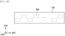
- FIG. 1 is a schematic plan view of an inkjet printing device according to one embodiment.
- an inkjet printing device 1000 includes a print head unit 100 including a plurality of inkjet heads 300 (see FIG. 2 ) and an electric field generation unit 700.
- the inkjet printing device 1000 may further include a base frame 600 and a stage STA.
- the inkjet printing device 1000 may spray a predetermined ink 90 (see FIG. 3 ) onto a target substrate SUB (see FIG. 3 ) by using the print head unit 100.
- An electric field may be generated by the electric field generation unit 700 on the target substrate SUB onto which the ink 90 is sprayed, and particles such as bipolar elements included in the ink 90 may be aligned on the target substrate SUB.
- the target substrate SUB may be provided on the electric field generation unit 700, the electric field generation unit 700 may form an electric field above the target substrate SUB, and the electric field may be transferred to the ink 90 sprayed on the target substrate SUB.
- Particles such as bipolar elements included in the ink 90 may have a shape extending in one direction, and may be aligned such that the extension direction faces one direction by the electric field.
- the inkjet printing device 1000 may include the inkjet head 300 to be described later, such that particles such as bipolar elements to be aligned on the target substrate SUB may be sprayed onto the target substrate SUB in a state of being oriented in an arbitrary direction.
- the inkjet head 300 may prevent a nozzle 350 from which the ink 90 is ejected from being clogged by the particles included in the ink 90.
- the inkjet printing device 1000 will be described in detail with reference to the drawings.
- a first direction DR1, a second direction DR2, and a third direction DR3 are defined.
- the first direction DR1 and the second direction DR2 are located on one plane and are orthogonal to each other, and the third direction DR3 is a direction perpendicular to the first direction DR1 and the second direction DR2.
- the first direction DR1 refers to a horizontal direction in the drawing
- the second direction DR2 refers to a vertical direction in the drawing
- the third direction DR3 refers to an upward and downward direction in the drawing.
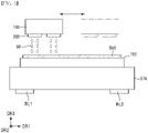
- FIG. 2 is a schematic plan view of a print head unit according to one embodiment.
- the inkjet printing device 1000 includes the print head unit 100 including the plurality of inkjet heads 300 and the electric field generation unit 700.
- the inkjet printing device 1000 may further include the stage STA on which the electric field generation unit 700 is disposed.
- the stage STA may provide a region in which the electric field generation unit 700 is disposed.
- the inkjet printing device 1000 includes a first rail RL1 and a second rail RL2 extending in the second direction DR2, and the stage STA is disposed on the first rail RL1 and the second rail RL2.
- the stage STA may move in the second direction DR2 through a separate moving member on the first rail RL1 and the second rail RL2.
- the electric field generation unit 700 may move together with the stage STA in the second direction DR2, and the ink 90 may be sprayed above the electric field generation unit 700 while the electric field generation unit 700 passes by the print head unit 100.
- the print head unit 100 may include the plurality of inkjet heads 300 and may be disposed on the base frame 600.
- the print head unit 100 may spray the predetermined ink 90 onto the target substrate SUB provided in the electric field generation unit 700 by using the inkjet head 300 connected to a separate ink storage unit.
- the ink 90 may include a solvent 91 and a plurality of bipolar elements 95 included in the solvent 91.
- the ink 90 may be provided in a solution or colloidal state.
- the solvent 91 may be acetone, water, alcohol, toluene, propylene glycol (PG), or propylene glycol methyl acetate (PGMA), or the like, but is not limited thereto.
- the plurality of bipolar elements 95 may be supplied to and ejected from the print head unit 100 while being included in a dispersed state in the solvent 91.
- the base frame 600 may include a support unit 610 and a moving unit 630.
- the support unit 610 may include a first support part 611 extending in the first direction DR1 which is the horizontal direction, and a second support part 612 connected to the first support part 611 and extending in the third direction DR3 which is the vertical direction.
- the extension direction of the first support part 611 may be the same as the first direction DR1 which is a long side direction of the electric field generation unit 700.
- the print head unit 100 may be disposed on the moving unit 630 mounted on the first support part 611.
- the moving unit 630 may include a moving part 631 mounted on the first support part 611 and movable in one direction and a fixing part 632 disposed on the bottom surface of the moving part 631 and on which the print head unit 100 is placed.
- the moving part 631 may move in the first direction DR1 on the first support part 611, and the print head unit 100 may be fixed to the fixing part 632 to move together with the moving part 631 in the first direction DR1.
- the print head unit 100 may be disposed on the base frame 600, and may spray the ink 90 provided from an ink reservoir onto the target substrate SUB through the inkjet head 300 to be described later.
- the print head unit 100 may be spaced apart from the stage STA passing below the base frame 600 by a predetermined distance.
- the distance between the print head unit 100 and the stage STA may be adjusted by the height of the second support part 612 of the base frame 600.
- the separation distance between the print head unit 100 and the stage STA may be adjusted within a range in which a process space can be secured due to a certain distance between the print head unit 100 and the target substrate SUB when the electric field generation unit 700 and the target substrate SUB are disposed on the stage STA.
- the print head unit 100 may include the inkjet head 300 including a plurality of nozzles 350.
- the inkjet head 300 may be disposed on the bottom surface of the print head unit 100.
- the plurality of inkjet heads 300 may be disposed to be spaced apart from each other in one direction, and may be arranged in one row or a plurality of rows.
- the drawing illustrates that the inkjet heads 300 are disposed in two rows and the inkjet heads 300 of each row are alternately disposed.
- the disclosure is not limited thereto, and the inkjet heads 300 may be arranged in a larger number of rows and may be disposed to overlap each other without crossing each other.
- the shape of the inkjet head 300 is not particularly limited, but as an example, the inkjet head 300 may have a quadrilateral shape.
- At least one inkjet head 300 may form one pack to be disposed adjacent to each other.
- the number of inkjet heads 300 included in one pack is not limited thereto, and for example, the number of inkjet heads 300 included in one pack may be one to five.
- the drawing illustrates only six inkjet heads 300 disposed in the print head unit 100, this is to schematically illustrate the print head unit 100, and the number of inkjet heads 300 is not limited thereto.
- the inkjet head 300 disposed in the print head unit 100 may spray the ink 90 onto the target substrate SUB disposed above the stage STA.
- the print head unit 100 may move on the first support part 611 in one direction, and the inkjet head 300 may move in the one direction to spray the ink 90 onto the target substrate SUB.
- FIG. 3 is a schematic view illustrating an operation of a print head unit according to one embodiment.
- FIG. 3 illustrates a front view of the print head unit 100 and the electric field generation unit 700 disposed on the stage STA according to one embodiment.
- the print head unit 100 may move in the first direction DR1 in which the first support part 611 extends, and the inkjet head 300 may move in the first direction DR1 and spray the ink 90 onto the target substrate SUB.
- a width of the target substrate SUB measured in the first direction DR1 may be greater than a width of the print head unit 100.
- the print head unit 100 may move in the first direction DR1 and spray the ink 90 over the entire surface of the target substrate SUB.
- the print head unit 100 may spray the ink 90 onto each of the plurality of target substrates SUB while moving in the first direction DR1.
- the print head unit 100 may be positioned on the outside of the first rail RL1 and the second rail RL2 and then move in the first direction DR1 to spray the ink 90 onto the target substrate SUB.
- the print head unit 100 may move between the first rail RL1 and the second rail RL2 to spray the ink 90 through the inkjet head 300.
- the operation of the inkjet head 300 is not limited thereto and may be modified in various ways within a range in which it can be implemented. A detailed description of the operation of the inkjet head 300 will be omitted.
- FIG. 4 is a schematic cross-sectional view of an inkjet head according to one embodiment.
- FIG. 5 is a cross-sectional view illustrating ink ejected from an inkjet head according to one embodiment.
- the inkjet head 300 may include the plurality of nozzles 350 to eject the ink 90 through the nozzles 350.
- the ink 90 ejected from the nozzle 350 may be sprayed to the target substrate SUB provided on the stage STA or the electric field generation unit 700.
- the nozzles 350 may be positioned on the bottom surface of the inkjet head 300 and may be arranged along one direction in which the inkjet head 300 extends.
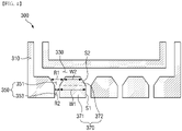
- the inkjet head 300 may include a base part 310, an inner tube 330 to which the ink 90 is supplied, a plurality of nozzles 350 connected to the inner tube 330 to eject the ink 90, and a guide part 370 positioned between the plurality of nozzles 350 of the base part 310.
- the base part 310 may be a part constituting a main body of the inkjet head 300.
- the base part 310 may be attached to the print head unit 100, and the inner tube 330 included in the base part 310 may be connected to the inner flow path of the print head unit 100 such that the ink 90 may be supplied.
- the base part 310 may have a shape extending in one direction, and the inner tube 330 may be formed along the extension direction of the base part 310.
- the ink 90 supplied through the print head unit 100 may be introduced along the inner tube 330 and may be ejected through the nozzle 350 of the inkjet head 300.
- the inkjet head 300 may include the plurality of nozzles 350, and the base part 310 may include the guide part 370 between the plurality of nozzles 350.
- the plurality of nozzles 350 may be arranged to be spaced apart from each other, and a portion of the base part 310 between the nozzles 350 may be the guide part 370.
- the plurality of nozzles 350 may be connected to the inner tube 330 and arranged along the extension direction of the base part 310. Although not illustrated in the drawings, the plurality of nozzles 350 may be arranged in one row or a plurality of rows. In addition, although the drawing illustrates that four nozzles 350 are formed in the inkjet head 300, the disclosure is not limited thereto. In some embodiments, the number of nozzles 350 included in the inkjet head 300 may range from 128 to 1800.
- the nozzle 350 may eject the ink 90 introduced along the inner tube 330.
- the amount of the ink 90 sprayed through the nozzles 350 may be adjusted according to a voltage applied to each nozzle 350.
- the amount of the ink 90 ejected once from each nozzle 350 may be 1 to 50 pico-liter (pL), but the disclosure is not limited thereto.
- the nozzle 350 may include an inlet 351 having a first diameter R1 and an outlet 353 connected to the inlet 351 and having a second diameter R2 smaller than the first diameter R1.
- the inlet 351 is directly connected to the inner tube 330, and is a portion in which the ink 90 flowing along the inner tube 330 is supplied to the nozzle 350.
- the outlet 353 is connected to the inlet 351, and the ink 90 supplied from the inlet 351 may be ejected through the outlet 353.
- the bipolar elements 95 dispersed in the ink 90 may have a shape extending in one direction.
- the bipolar elements 95 randomly dispersed in the ink 90 may flow along the inner tube 330 and then be supplied to the nozzle 350.
- the bipolar elements 95 in the ink 90 may be supplied to the nozzle 350 in a clustered state, and a phenomenon may occur in which the entrance of the nozzle 350 is clogged.
- the inkjet head 300 may include the inlet 351 having the first diameter R1 that is larger than the second diameter R2 of the outlet 353, to prevent the nozzle 350 from being clogged by the bipolar elements 95.
- the first diameter R1 of the inlet 351 may be greater than the length of the long axis of the bipolar element 95, but is not limited thereto.
- the orientation direction of the plurality of bipolar elements 95 which is a direction that the long axis faces, may be determined.
- the plurality of bipolar elements 95 may be supplied to the inner tube 330 in a state having random orientation directions in the ink 90.
- the direction that the long axis of the bipolar element 95 faces that is, the orientation direction may be changed according to the shape of the inlet 351.
- the nozzle 350 of the inkjet head 300 may have an inclined side surface in at least some regions.
- a first side surface S1 that is one side surface of the outlet 353 may extend in one direction
- a second side surface S2 that is one side surface of the inlet 351 may be formed to be inclined with respect to the one direction.
- the first diameter R1 of the inlet 351 may decrease from the inner tube 330 toward the outlet 353.
- the inlet 351 has a larger diameter than the outlet 353, and the portion adjacent to the outlet 353 has a smaller diameter than the portion adjacent to the inner tube 330, so that the second side surface S2 may be formed to be inclined.
- the ink 90 supplied from the inner tube 330 to the nozzle 350 may flow along the inclined side surface of the inlet 351.
- the bipolar elements 95 dispersed in the ink 90 flow along the second side surface S2 of the inlet 351, and as the bipolar elements 95 having random orientation directions flow along the second side surface S2, the orientation direction thereof may change.
- the bipolar elements 95 extending in one direction the direction of the long axis thereof may change in parallel with the inclined direction of the second side surface S2. Accordingly, the bipolar elements 95 dispersed in the ink 90 may have an orientation direction facing an arbitrary one direction.
- the first side surface S1 may extend in one direction.
- the ink 90 introduced through the inlet 351 may be ejected without changing the orientation direction while flowing along the first side surface S1 of the outlet 353.
- the bipolar elements 95 introduced into the outlet 353 may have an arbitrary orientation direction while flowing along the second side surface S2 of the inlet 351, and may be ejected from the outlet 353 in a state having the orientation direction.
- the bipolar element 95 ejected from the inkjet head 300 may be ejected in a state in which the direction of the long axis is parallel to one direction in which the first side surface S1 of the outlet 353 extends.
- the bipolar elements 95 supplied to the inner tube 330 flow with a random orientation direction.
- the bipolar elements 95 introduced into the outlet 353 through the inlet 351 of the nozzle 350 may be oriented such that one direction of extension is parallel to one direction in which the first side surface S1 extends.
- the ink 90 ejected from the nozzle 350 of the inkjet head 300 may include the plurality of bipolar elements 95 having an arbitrary orientation direction in a dispersed state.
- the base part 310 of the inkjet head 300 may include the guide part 370 which is a portion positioned between the nozzles 350, and the shapes of the side surfaces S1 and S2 and the diameters R1 and R2 of the inlet 351 and the outlet 353 may be determined according to the shape of the guide part 370.
- the inkjet head 300 may include the guide part 370 positioned between the plurality of nozzles 350, and the guide part 370 may include a first guide part 371 between the outlets 353 and a second guide part 372 between the inlets 351.
- the diameter R1 of the inlet 351 may be greater than the diameter R2 of the outlet 353, and similarly, a first width W1 of the first guide part 371 may be greater than a second width W2 of the second guide part 372.
- the second width W2 of the second guide part 372 may increase from the inner tube 330 toward the first guide part 371. Accordingly, the first diameter R1 of the inlet 351 between the second guide parts 372 may be changed, and an inclined side surface may be formed.
- the nozzle 350 having the first side surface S1 and the second side surface S2 may eject the ink 90 in a state in which the plurality of bipolar elements 95 have an arbitrary orientation direction, and as described above, the ink 90 ejected from the inkjet head 300 may be sprayed onto the target substrate SUB.
- FIG. 6 is a schematic view illustrating ink ejected from an inkjet head according to one embodiment.
- the ink 90 ejected from the inkjet head 300 is sprayed onto the target substrate SUB.
- the bipolar elements 95 having a random orientation in the inner tube 330 may be ejected with an arbitrary orientation direction through the nozzle 350.
- the ink 90 may be ejected from the inkjet head 300 in a state in which the orientation direction of the long axis of the bipolar element 95 is perpendicular to the top surface of the target substrate SUB.
- the direction of the long axes of the bipolar elements 95 may face the top surface of the target substrate SUB.
- the bipolar elements 95 may be sprayed onto the target substrate SUB with an arbitrary orientation direction, and may be placed on the target substrate SUB with a specific orientation direction by the electric field generated by the electric field generation unit 700.
- the bipolar element 95 may include a first end having a first polarity and a second end having a second polarity.
- a specific orientation direction may be defined based on the direction that the first end faces.
- the bipolar elements 95 dispersed in the ink 90 are illustrated to face the upward direction and the downward direction in the drawing without a uniform direction that the first end faces.
- the disclosure is not limited thereto.
- the inkjet head 300 may further include a member for generating an electric field in the nozzle 350 such that the first ends of the bipolar elements 95 dispersed in the ink 90 face the same direction. A description thereof may refer to other embodiments.
- the electric field generation unit 700 may generate an electric field above the target substrate SUB.
- the bipolar elements 95 included in the ink 90 may be aligned to have a specific orientation direction.
- the electric field generation unit 700 will be described with reference to other drawings.
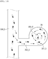
- FIG. 7 is a schematic plan view of an electric field generation unit according to one embodiment.
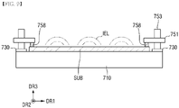
- the electric field generation unit 700 may include a sub-stage 710, a probe support 730, a probe unit 750, and an aligner 780.
- the electric field generation unit 700 may be disposed on the stage STA and may move in the second direction DR2 together with the stage STA.
- the electric field generation unit 700 on which the target substrate SUB is disposed may move along the stage STA, and the ink 90 may be sprayed above the electric field generation unit 700.
- the electric field generation unit 700 may generate an electric field above the target substrate SUB when the ink 90 is sprayed.
- the sub-stage 710 may provide a space where the target substrate SUB is disposed.
- the probe support 730, the probe unit 750, and the aligner 780 may be disposed on the sub-stage 710.
- the shape of the sub-stage 710 is not particularly limited, but for example, as illustrated in the drawing, the sub-stage 710 may have a quadrilateral shape with both sides extending in the first direction DR1 and the second direction DR2.
- the sub-stage 710 may include long sides extending in the first direction DR1 and short sides extending in the second direction DR2.
- the overall planar shape of the sub-stage 710 may vary depending on the shape of the target substrate SUB in plan view.
- the shape of the sub-stage 710 may be rectangular as illustrated in the drawing, and when the target substrate SUB has a circular planar shape, the sub-stage 710 may also have a circular shape in plan view.
- At least one aligner 780 may be disposed on the sub-stage 710.
- the aligner 780 may be disposed on each side of the sub-stage 710, and a region surrounded by the plurality of aligners 780 may be a region in which the target substrate SUB is disposed.
- two aligners 780 are disposed to be spaced apart on each side of the sub-stage 710, and a total of eight aligners 780 are disposed on the sub-stage 710.
- the disclosure is not limited thereto, and the number, disposition, or the like of the aligners 780 may vary depending on the shape or type of the target substrate SUB.
- the probe support 730 and the probe unit 750 are disposed on the sub-stage 710.
- the probe support 730 may provide a space in which the probe unit 750 is disposed on the sub-stage 710.
- the probe support 730 may be disposed on at least one side of the sub-stage 710 and extend along the direction in which the one side portion extends.
- the probe support 730 may be disposed to extend in the second direction DR2 on the left and right sides of the sub-stage 710.
- the disclosure is not limited thereto, and a larger number of probe supports 730 may be included, and in some cases, may also be disposed on the upper and lower sides of the sub-stage 710. That is, the structure of the probe support 730 may vary according to the number, disposition, structure, or the like of the probe units 750 included in the electric field generation unit 700.
- the probe unit 750 may be disposed on the probe support 730 to form an electric field on the target substrate SUB prepared on the sub-stage 710. Like the probe support 730, the probe unit 750 may extend in one direction, for example, the second direction DR2, and the extension length may cover the entire target substrate SUB. That is, the size and shape of the probe support 730 and the probe unit 750 may vary depending on the target substrate SUB.
- the probe unit 750 may include a probe driver 753 disposed on the probe support 730, a probe jig 751 disposed on the probe driver 753 to receive an electrical signal, and a probe pad 758 connected to the probe jig 751 to transmit the electrical signal to the target substrate SUB.
- the probe driver 753 may be disposed on the probe support 730 to move the probe jig 751 and the probe pad 758.
- the probe driver 753 may move the probe jig 751 in a horizontal direction and a vertical direction, for example, the first direction DR1 which is the horizontal direction and the third direction DR3 which is the vertical direction.
- the probe pad 758 may be connected to or separated from the target substrate SUB by the driving of the probe driver 753.
- the probe driver 753 may be driven to connect the probe pad 758 to the target substrate SUB, and in other steps, the probe driver 753 may be driven again to separate the probe pad 758 from the target substrate SUB. A detailed description thereof will be given later with reference to other drawings.
- the probe pad 758 may form an electric field on the target substrate SUB through an electrical signal transmitted from the probe jig 751.
- the probe pad 758 may be connected to the target substrate SUB and transmit the electrical signal to form an electric field on the target substrate SUB.
- the probe pad 758 may be in contact with an electrode or a power pad of the target substrate SUB, and an electrical signal of the probe jig 751 may be transmitted to the electrode or the power pad.
- the electrical signal transmitted to the target substrate SUB may form an electric field on the target substrate SUB.
- the probe pad 758 may be a member that forms an electric field through an electrical signal transmitted from the probe jig 751. That is, when the probe pad 758 receives the electrical signal to form an electric field, the probe pad 758 may not be connected to the target substrate SUB.
- the shape of the probe pad 758 is not particularly limited, but in an embodiment, the probe pad 758 may have a shape extending in one direction to cover the entire target substrate SUB.
- the probe jig 751 may be connected to the probe pad 758 and may be connected to a separate voltage applying device.
- the probe jig 751 may transmit an electrical signal transmitted from the voltage applying device to the probe pad 758 to form an electric field on the target substrate SUB.
- the electrical signal transmitted to the probe jig 751 may be a voltage for forming an electric field, for example, an alternating current (AC) voltage.
- AC alternating current
- the probe unit 750 may include a plurality of probe jigs 751 and the number thereof is not particularly limited. Although the drawing illustrates that three probe jigs 751 and three probe driver 753 are disposed, the probe unit 750 may include a larger number of probe jigs 751 and probe drivers 753 to form an electric field having a higher density on the target substrate SUB.
- the probe unit 750 is not limited thereto. Although the drawing illustrates that the probe unit 750 is disposed on the probe support 730, that is, the electric field generation unit 700, the probe unit 750 may be disposed as a separate device in some cases. As long as the electric field generation unit 700 includes a device capable of forming an electric field and may form an electric field on the target substrate SUB, the structure or disposition thereof is not limited.
- FIGS. 8 and 9 are schematic views illustrating an operation of a probe unit according to one embodiment.
- the probe driver 753 of the probe unit 750 may be operated according to a process step of the inkjet printing device 1000. Referring to FIGS. 8 and 9 , in a first state in which no electric field is formed in the electric field generation unit 700, the probe unit 750 may be disposed on the probe support 730 to be spaced apart from the target substrate SUB. The probe driver 753 of the probe unit 750 may be driven in the second direction DR2 that is the horizontal direction and in the third direction DR3 that is the vertical direction, to separate the probe pad 758 from the target substrate SUB.
- the probe driver 753 of the probe unit 750 may be driven to connect the probe pad 758 to the target substrate SUB.
- the probe driver 753 may be driven in the third direction DR3 that is the vertical direction and in the first direction DR1 that is the horizontal direction such that the probe pad 758 may be in contact with the target substrate SUB.
- the probe jig 751 of the probe unit 750 may transmit an electrical signal to the probe pad 758, and an electric field may be formed on the target substrate SUB.
- any first probe unit 750 may first form an electric field on the target substrate SUB, and a second probe unit 750 may not be connected to the target substrate SUB. Thereafter, the first probe unit 750 may be separated from the target substrate SUB and the second probe unit 750 may be connected to the target substrate SUB to form an electric field. That is, the plurality of probe units 750 may be simultaneously driven to form an electric field, or each may be sequentially driven to sequentially form an electric field.
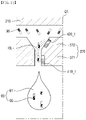
- FIG. 10 is a schematic view illustrating that an electric field is generated on a target substrate by an electric field generation unit according to one embodiment.
- the bipolar element 95 may be an object having one end having a first polarity and the other end having a second polarity different from the first polarity.
- one end of the bipolar element 95 may have a positive polarity, and the other end of the bipolar element 95 may have a negative polarity.
- the bipolar element 95 having different polarities at both ends may receive electric forces (attractive and repulsive forces) when placed in a predetermined electric field, and the orientation direction thereof may be controlled.
- the ink 90 including the bipolar elements 95 is ejected from the nozzle 350 of the inkjet head 300.
- the ink 90 ejected from the nozzle 350 may be sprayed onto the target substrate SUB including the bipolar elements 95 having an arbitrary orientation direction.
- the bipolar element 95 having the first polarity and the second polarity may receive an electric force until the ink 90 is placed on the target substrate SUB or even after placed.
- the bipolar element 95 may be oriented according to the polarities of the first end and the second end.
- the orientation direction of the bipolar element 95 may be a direction that the electric field IEL faces.
- the bipolar element 95 ejected from the inkjet head 300 may be oriented such that the direction of the long axis thereof is perpendicular to the top surface of the target substrate SUB.
- the electric field IEL generated on the target substrate SUB may be formed in a direction horizontal to the top surface of the target substrate SUB, and the orientation direction and position of the first end and the second end of the bipolar element 95 may be changed along the direction of the electric field IEL.
- the bipolar element 95 sprayed onto the target substrate SUB may be oriented such that by the electric field IEL, the extension direction faces a direction different from the direction perpendicular to the top surface of the target substrate SUB.
- the bipolar element 95 extending in one direction may be oriented such that the first end and the second end face a direction horizontal to the target substrate SUB.
- the bipolar element 95 may be oriented such that the first end having the first polarity faces one direction, and the second end having the second polarity faces the other direction.
- the bipolar element 95 ejected from the inkjet head 300 may be oriented such that the direction of the long axis thereof is perpendicular to the top surface of the target substrate SUB but the first end of each bipolar element 95 faces a random direction.
- each of the bipolar elements 95 may be oriented such that the first ends thereof face the same direction and may be aligned on the target substrate SUB.
- the inkjet printing device 1000 may align the bipolar elements 95 on the target substrate SUB such that the first end has a specific direction.
- the bipolar elements 95 ejected from the inkjet head 300 have an arbitrary orientation direction, the bipolar elements 95 may be smoothly aligned according to the direction of the electric field IEL generated on the target substrate SUB.
- the orientation error of the other bipolar elements 95 may be calculated, and the alignment degree of the oriented bipolar elements 95 may be measured based thereon.
- the 'alignment degree' of the bipolar elements 95 may mean a degree of error between orientation directions of the bipolar elements 95 aligned on the target substrate SUB.
- the alignment degree of the bipolar elements 95 is low, and when the error between the orientation directions of the bipolar elements 95 is small, the alignment degree of the bipolar elements 95 is high or improved.
- the inkjet printing device 1000 may eject the bipolar element 95 in a state having an arbitrary orientation direction, and the alignment degree of the bipolar element 95 to be aligned on the target substrate SUB may be improved.
- a time point at which the electric field generation unit 700 generates the electric field IEL above the target substrate SUB is not particularly limited.
- the drawing illustrates that the probe unit 750 generates the electric field IEL while the ink 90 is ejected from the nozzle 350 and reaches the target substrate SUB.
- the bipolar element 95 may receive a force due to the electric field IEL until the bipolar element 95 is ejected from the nozzle 350 and reaches the target substrate SUB.
- the disclosure is not limited thereto, and in some cases, the probe unit 750 may generate the electric field IEL after the ink 90 is sprayed onto the target substrate SUB.
- the electric field generation unit 700 may generate the electric field IEL when the ink 90 is sprayed from the inkjet head 300 or thereafter.
- an electric field generation member may be further disposed on the sub-stage 710.
- the electric field generation member may form an electric field in an upward direction (i.e., the third direction DR3) or above the target substrate SUB, like the probe unit 750 to be described later.
- an antenna unit or a device including a plurality of electrodes may be applied as the electric field generation member.
- the inkjet printing device 1000 may further include a heat treatment unit in which a process of volatilizing the ink 90 sprayed onto the target substrate SUB is performed.
- the heat treatment unit may irradiate heat to the ink 90 sprayed onto the target substrate SUB such that the solvent 91 of the ink 90 is volatilize and removed, and the bipolar element 95 may be disposed on the target substrate SUB.
- the process of removing the solvent 91 by irradiating heat to the ink 90 may be performed by using a conventional heat treatment unit. A detailed description thereof will be omitted.
- the inkjet printing device 1000 may include the nozzle 350 in which the inkjet head 300 has the inclined second side surface S2 such that the bipolar elements 95 may be ejected in an arbitrary orientation direction.
- the bipolar elements 95 may have an arbitrary orientation direction and be dispersed, and the bipolar elements 95 may be aligned in a specific orientation direction by the electric field IEL generated by the electric field generation unit 700.
- the inkjet printing device 1000 may improve the alignment degree of the bipolar element 95 aligned on the target substrate SUB.
- the bipolar element 95 may include a first end having a first polarity and a second end having a second polarity, and may have a specific orientation direction that the first end faces.
- the inkjet head 300 according to one embodiment further includes a member generating the electric field IEL in the nozzle 350 such that the bipolar elements 95 to be ejected may be induced to have a specific orientation direction with the first ends thereof facing the same direction.
- FIG. 11 is a schematic cross-sectional view of an inkjet head according to another embodiment.
- FIG. 12 is an enlarged view of part Q1 of FIG. 11 .
- an inkjet head 300_1 may further include an electric field generation electrode 400_1 disposed on the guide part 370.
- the electric field generation electrode 400_1 may generate the electric field IEL in the nozzle 350 by an applied electrical signal.
- the bipolar element 95 ejected through the nozzle 350 may be aligned such that the first end and the second end having polarities face a specific direction by the electric field IEL generated by the electric field generation electrode 400_1.
- the electric field generation electrode 400_1 disposed on the guide part 370 may be further included such that the plurality of bipolar elements 95 dispersed in the ink 90 may be ejected in an aligned state so that the first ends face the same direction. Descriptions of the other members are the same as those of the embodiment of FIG. 4 , and thus hereinafter, redundant description will be omitted while focusing on differences.
- the electric field generation electrode 400_1 may be disposed on a side surface of the guide part 370.
- the electric field generation electrode 400_1 may include a first electric field generation electrode 410_1 and a second electric field generation electrode 420_1, the first electric field generation electrode 410_1 may be disposed on one side surface of the first guide part 371, and the second electric field generation electrode 420_1 may be disposed on one side surface of the second guide part 372.
- the first electric field generation electrode 410_1 may be disposed on one side surface of the first guide part 371 to be disposed on the first side surface S1 of the outlet 353, and the second electric field generation electrode 420_1 may be disposed on one side surface of the second guide part 372 to be disposed on the second side surface S2 of the inlet 351.
- the first side surface S1 of the outlet 353 may have a shape extending in one direction, and the second side surface S2 of the inlet 351 may be formed to be inclined. Accordingly, the first electric field generation electrode 410_1 may be disposed on a side surface extending in one direction, and the second electric field generation electrode 420_1 may be disposed on a side surface formed to be inclined.
- the first electric field generation electrode 410_1 and the second electric field generation electrode 420_1 may be spaced apart from each other in one direction.
- the first electric field generation electrode 410_1 and the second electric field generation electrode 420_1 may be disposed to be spaced apart from each other along side surfaces of the nozzle 350.
- the first electric field generation electrode 410_1 may be disposed below the second electric field generation electrode 420_1.
- the first electric field generation electrode 410_1 and the second electric field generation electrode 420_1 may perform substantially the same function as the probe unit 750 of the electric field generation unit 700. However, the electric field generation electrode 400_1 is different from the electric field generation unit 700 in that the electric field generation electrode 400_1 is directly disposed in the inkjet head 300.
- a predetermined electrical signal may be applied to the first electric field generation electrode 410_1 and the second electric field generation electrode 420_1, and an electric field IEL may be generated therebetween.
- the first electric field generation electrode 410_1 and the second electric field generation electrode 420_1 may generate the electric field IEL that faces one direction in which the first side surface S1 extends, at the inlet 351 and the outlet 353.
- the electric field IEL may align the bipolar elements 95 dispersed in the ink 90 such that the first ends having the first polarities face the same direction.
- 11 and 12 may further include the electric field generation electrode 400_1 such that the bipolar elements 95 to be ejected may be aligned with a specific orientation direction so that the first ends have the same direction. Accordingly, the bipolar elements 95, which are aligned such that the first ends thereof face the same direction, may be dispersed in the ink 90 that is sprayed onto the target substrate SUB, and the bipolar element 95 may be smoothly aligned by the electric field IEL generated by the electric field generation unit 700. That is, the inkjet printing device 1000 further including the electric field generation electrode 400_1 may further improve the alignment degree of the bipolar element 95.
- FIG. 13 is a schematic cross-sectional view illustrating another example of the inkjet head of FIG. 11 .
- FIG. 14 is a schematic cross-sectional view illustrating still another example of the inkjet head of FIG. 11 .
- an inkjet head 300_2 may include a larger number of electric field generation electrodes 400_2.
- a first electric field generation electrode 410_2 may be disposed on both side surfaces of the first guide part 371, and a second electric field generation electrode 420_2 may be disposed on both side surfaces of the second guide part 372. Accordingly, a stronger electric field IEL may be generated in the nozzle 350 of the inkjet head 300_2, and the bipolar elements 95 may be ejected from the inkjet head 300_2 in an aligned state with a specific orientation direction.
- the embodiment is different from the embodiment of FIG. 11 in that a larger number of electric field generation electrodes 400_2 are disposed.
- electric field generation electrodes 400_3 may be disposed to surround the nozzle 350. Accordingly, the uniform electric field IEL may be generated in the nozzle 350 of the inkjet head 300_3 according to the position, and the bipolar elements 95 may receive a force uniformly generated by the electric field IEL until the bipolar elements 95 are ejected through the nozzle 350.
- the embodiment is different from the embodiment of FIG. 13 in that the disposition of the electric field generation electrode 400_3 is different. Hereinafter, redundant description will be omitted.
- FIG. 15 is a schematic cross-sectional view of an inkjet head according to still another embodiment.
- FIG. 16 is an enlarged view of part Q2 of FIG. 15 .
- an inkjet head 300_4 may include an electric field generation coil 500_4 disposed to surround the nozzle 350.
- the electric field generation coil 500_4 may generate the electric field IEL in one direction in which the coil extends, by the flowing current.
- the electric field generation coil 500_4 disposed to surround at least the outlet 353 in the nozzles 350 may generate the electric field IEL along one direction in which the first side surface S1 of the outlet 353 extends.
- the bipolar elements 95 introduced into the nozzle 350 may have a first end and a second end that are oriented according to the direction of the electric field IEL, and may be ejected from the inkjet head 300_4 in an aligned state having a specific orientation direction.
- the embodiment is different from the embodiment of FIG. 11 in that the member generating the electric field IEL in the nozzle 350 of the inkjet head 300_4 is the electric field generation coil 500_4.
- redundant description will be omitted.
- FIG. 17 is a schematic cross-sectional view of an inkjet head according to still another embodiment.
- FIG. 18 is a schematic view illustrating ink flowing in the inkjet head of FIG. 17 .
- an inkjet head 300_5 may further include a plurality of third guide parts 380_5 disposed between an inlet 351_5 and an inner tube 330_5, and a nozzle 350_5 may further include an inlet tube 355_5 formed by a separation space between the third guide parts 380_5 between the inner tube 330 and the inlet 351_5.
- the embodiment is different from the embodiment of FIG. 5 in that the inkjet head 300_5 further includes the third guide part 380_5 such that the ink 90 flowing along the inner tube 330 is supplied to the inlet 351_5 through the inlet tube 355_5.
- redundant description will be omitted while focusing on differences.
- the third guide part 380_5 may be disposed on the second guide part 372_5.
- the third guide part 380_5 may have a shape extending in one direction and may protrude from one side surface of the inlet 351_5 toward the other side surface.
- a first guide part 371_5 and a second guide part 372_5 may be positioned between the plurality of nozzles 350_5, and the third guide part 380_5 may also be disposed between the plurality of nozzles 350_5.
- the inkjet head 300_5 may include the plurality of third guide parts 380_5, which may be spaced apart from each other.
- the third guide part 380_5 may be disposed between the inner tube 330 and the inlet 351_5 of the nozzle 350_5, and the inlet tube 355_5 may be formed in a space where the third guide parts 380_5 are spaced apart.
- the entrance of the inlet 351_5 through which the ink 90 is supplied from the inner tube 330 may be narrowed. That is, a third diameter R3 that is the diameter of the inlet tube 355_5 may be smaller than the first diameter R1 that is the diameter of the inlet 351_5.
- the ink 90 flowing along the inner tube 330 may be supplied to the inlet 351_5 through the inlet tube 355_5 having a narrow diameter.
- the flow rate of the ink 90 increases while flowing through the inlet tube 355_5, and the ink 90 may be introduced into an outlet 353_5 with an increased flow rate along the inclined side surface of the inlet 351_5.
- FIG. 18 schematically illustrates that the ink 90 is supplied to the inlet 351_5 through the inlet tube 355_5 formed by the third guide part 380_5.
- the third guide part 380_5 is positioned above and below the inlet tube 355_5.
- the ink 90 flowing along the inner tube 330_5 may be supplied to the inlet 351_5 through the inlet tube 355_5.
- the ink 90 supplied from the inner tube 330_5 having a relatively wide diameter to the inlet tube 355_5 having a narrow diameter flows along the side surface of the inlet 351_5 with a high flow rate.
- the ink 90 may flow while rotating along the side surface of the inlet 351_5, and may be introduced into the outlet 353_5 in a state having a rotational force.
- the inlet 351_5 may be formed such that the second side surface S2, which is one side surface, is inclined, and the bipolar elements 95 dispersed in the ink 90 having a high flow rate may have an arbitrary orientation direction.
- the inkjet head 300_5 may further include the third guide part 380_5 to induce the bipolar element 95 to be ejected from the nozzle 350_5 with an arbitrary orientation direction. Thereafter, when the bipolar element 95 is sprayed onto the target substrate SUB, the bipolar element 95 may be aligned to have a specific orientation direction by the electric field IEL generated by the electric field generation unit 700.
- redundant description will be omitted.
- the inkjet printing device 1000 described above may eject the ink 90 having a state in which the bipolar elements 95 are arranged in an arbitrary direction.
- the ink 90 having a state in which the bipolar elements 95 are arranged is sprayed onto the target substrate SUB, and the electric field generation unit 700 generates the electric field IEL above the target substrate SUB onto which the ink 90 is sprayed.
- the orientation direction and position of the bipolar element 95 may be changed by the electric field IEL, and the bipolar element 95 may be aligned in a specific direction on the target substrate SUB.
- a method for aligning the bipolar element 95 using the inkjet printing device 1000 according to one embodiment will be described in detail.
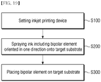
- FIG. 19 is a flowchart illustrating a method for aligning a bipolar element according to one embodiment.
- FIGS. 20 to 23 are cross-sectional views illustrating a method for aligning a bipolar element by using an inkjet printing device according to one embodiment.
- the method for aligning the bipolar element 95 may include setting the inkjet printing device 1000 (step S100), spraying the ink 90 including the bipolar element 95 oriented in one direction onto the target substrate SUB (step S200), and placing the bipolar element 95 on the target substrate SUB (step S300).
- the method for aligning the bipolar element 95 may be performed using the inkjet printing device 1000 described above with reference to FIG. 1 , and when the ink 90 is sprayed on the target substrate SUB, the bipolar elements 95 may be ejected in a state of being oriented in an arbitrary one direction. Thereafter, the bipolar elements 95 may be aligned in one direction by the electric field IEL generated above the target substrate SUB.
- the step S100 of setting the inkjet printing device 1000 is a step of tuning the inkjet printing device 1000 according to a target process. For precise tuning, an inkjet print test process is performed on an inspection substrate, and a setting value of the inkjet printing device 1000 may be adjusted according to the result.
- the inspection substrate may have the same structure as the target substrate SUB, but a bare substrate such as a glass substrate may be used.
- the top surface of the inspection substrate is treated with a water repellent treatment.
- the water repellent treatment may be performed by fluorine coating or plasma surface treatment.
- the ink 90 including the bipolar element 95 is sprayed onto the top surface of the inspection substrate using the inkjet printing device 1000, and a droplet amount for each inkjet head 300 is measured.
- the measurement of the droplet amount for each inkjet head 300 may be performed by using a camera to check the size of the droplet at the moment the droplet is sprayed and the size of the droplet applied to the substrate.
- the voltage for each corresponding inkjet head 300 is adjusted such that the reference droplet amount may be ejected.
- Such an inspection method may be repeated several times until each inkjet head 300 ejects an accurate droplet amount.
- step S100 of setting the inkjet printing device may be omitted.
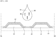
- the target substrate SUB is prepared.
- the first electrode 21 and the second electrode 22 may be disposed on the target substrate SUB.
- the drawing illustrates that a pair of electrodes are disposed, a larger number of electrode pairs may be formed on the target substrate SUB, and the plurality of inkjet heads 300 may spray the ink 90 to each electrode pair in the same manner.
- the ink 90 including the solvent 91 in which the bipolar elements 95 are dispersed is sprayed on the target substrate SUB (step S200).
- the ink 90 may be ejected from the inkjet head 300 of the print head unit 100, and may be sprayed onto the first electrode 21 and the second electrode 22 disposed on the target substrate SUB.
- the inkjet head 300 may include the nozzle 350 including the inlet 351 and the outlet 353 that have different widths, and the bipolar elements 95 dispersed in the ink 90 may be ejected in a state of being oriented in one direction.
- the ink 90 may be sprayed onto the first electrode 21 and the second electrode 22 disposed on the target substrate SUB, and one direction in which the bipolar elements 95 dispersed in the ink 90 extend may be oriented in a direction perpendicular to the top surface of the target substrate SUB.
- each of the bipolar elements 95 dispersed in the ink 90 may be sprayed in an aligned state in which the first end having the first polarity or the second end having the second polarity have the same direction. A description thereof is the same as that described above, and thus a detailed description thereof will be omitted.
- the electric field IEL is generated on the target substrate SUB, and the bipolar element 95 is placed on the target substrate SUB by the electric field IEL (step S300).
- the bipolar element 95 may be disposed between the first electrode 21 and the second electrode 22 by receiving a dielectrophoretic force by the electric field IEL generated above the target substrate SUB.
- an electrical signal is applied to the first electrode 21 and the second electrode 22 using the probe unit 750.
- the probe unit 750 may be connected to a predetermined pad (not shown) provided on the target substrate SUB, and may apply an electrical signal to the first electrode 21 and the second electrode 22 connected to the pad.
- the electrical signal may be an AC voltage, and the AC voltage may have a voltage of ⁇ (10 to 50) V and a frequency of 10 kHz to 1 MHz.
- the bipolar element 95 receives the dielectrophoretic force caused by the electric field IEL.
- the bipolar element 95 receiving the dielectrophoretic force may be disposed on the first electrode 21 and the second electrode 22 while the orientation direction and position thereof are changed.
- the orientation direction of the bipolar elements 95 dispersed in the ink 90 such that one direction of extension is perpendicular to the target substrate SUB may be changed according to the direction of the electric field IEL.
- the bipolar element 95 may be aligned by the electric field IEL such that one direction of extension faces the direction that the electric field IEL faces.
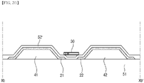
- the bipolar element 95 may be aligned such that the extension direction is parallel to the target substrate SUB and may be disposed between the first electrode 21 and the second electrode 22.
- the step of placing the bipolar element 95 is a step of placing the bipolar element 95 between the first electrode 21 and the second electrode 22, and at least one end of the bipolar element 95 may be disposed on at least one of the first electrode 21 or the second electrode 22.
- the disclosure is not limited thereto, and the bipolar element 95 may be directly disposed on the target substrate SUB between the first electrode 21 and the second electrode 22.
- the solvent 91 of the ink 90 sprayed onto the target substrate SUB is removed.
- the step of removing the solvent 91 is performed through a heat treatment device, and the heat treatment device may irradiate the target substrate SUB with heat H or infrared rays. Since the solvent 91 is removed from the ink 90 sprayed onto the target substrate SUB, the flow of the bipolar element 95 may be prevented and the bipolar element 95 may be placed on the electrodes 21 and 22.
- the inkjet printing device 1000 may align the bipolar element 95 on the target substrate SUB.
- the above-described bipolar element 95 may be a light emitting element including a plurality of semiconductor layers, and according to one embodiment, a display device including the light emitting element may be manufactured using the inkjet printing device 1000.
- FIG. 24 is a schematic view of a light emitting element according to one embodiment.
- the light emitting element 30 may be a light emitting diode.
- the light emitting element 30 may be an inorganic light emitting diode that has a micrometer or nanometer size, and is made of an inorganic material.
- the inorganic light emitting diode may be aligned between two electrodes having polarity when an electric field is formed in a specific direction between two electrodes opposing each other.
- the light emitting element 30 may be aligned between two electrodes by the electric field generated between the electrodes.
- the light emitting element 30 may have a shape extending in one direction.
- the light emitting element 30 may have a shape of a rod, wire, tube, or the like.
- the light emitting element 30 may have a cylindrical or rod shape.
- the shape of the light emitting element 30 is not limited thereto, and the light emitting element 30 may have a polygonal prism shape such as a regular cube, a rectangular parallelepiped and a hexagonal prism, or may have various shapes such as a shape extending in one direction and having an outer surface partially inclined.
- a plurality of semiconductors included in the light emitting element 30 to be described later may have a structure in which they are sequentially arranged or stacked along the one direction.
- the light emitting element 30 may include a semiconductor layer doped with any conductivity type (e.g., p-type or n-type) impurities.
- the semiconductor layer may emit light of a specific wavelength band by receiving an electrical signal applied from an external power source.
- the light emitting element 30 may include a first semiconductor layer 31, a second semiconductor layer 32, an active layer 33, an electrode layer 37, and an insulating film 38.
- the first semiconductor layer 31 may be an n-type semiconductor.
- the first semiconductor layer 31 may include a semiconductor material having a chemical formula of AlxGayIn1-x-yN (0 ⁇ x ⁇ 1, 0 ⁇ y ⁇ 1, 0 ⁇ x+y ⁇ 1).
- it may be any one or more of n-type doped AlGaInN, GaN, AlGaN, InGaN, AlN and InN.
- the first semiconductor layer 31 may be doped with an n-type dopant.
- the n-type dopant may be Si, Ge, Sn, or the like.
- the first semiconductor layer 31 may be n-GaN doped with n-type Si.
- the length of the first semiconductor layer 31 may have a range of 1.5 ⁇ m to 5 ⁇ m, but is not limited thereto.
- the second semiconductor layer 32 is disposed on the active layer 33 to be described later.
- the second semiconductor layer 32 may be a p-type semiconductor.
- the second semiconductor layer 32 may include a semiconductor material having a chemical formula of AlxGayIn1-x-yN (0 ⁇ x ⁇ 1, 0 ⁇ y ⁇ 1, 0 ⁇ x+y ⁇ 1).
- it may be any one or more of p-type doped AlGaInN, GaN, AlGaN, InGaN, AlN and InN.
- the second semiconductor layer 32 may be doped with a p-type dopant.
- the p-type dopant may be Mg, Zn, Ca, Se, Ba, or the like.
- the second semiconductor layer 32 may be p-GaN doped with p-type Mg.
- the length of the second semiconductor layer 32 may have a range of 0.05 ⁇ m to 0.10 ⁇ m, but is not limited thereto.
- the first semiconductor layer 31 and the second semiconductor layer 32 are configured as one layer, the disclosure is not limited thereto. According to some embodiments, depending on the material of the active layer 33, the first semiconductor layer 31 and the second semiconductor layer 32 may further include a larger number of layers, such as a cladding layer or a tensile strain barrier reducing (TSBR) layer. A description thereof will be given later with reference to other drawings.
- TSBR tensile strain barrier reducing
- the active layer 33 is disposed between the first semiconductor layer 31 and the second semiconductor layer 32.
- the active layer 33 may include a material having a single or multiple quantum well structure.
- the active layer 33 includes a material having a multiple quantum well structure, a plurality of quantum layers and well layers may be stacked alternately.
- the active layer 33 may emit light by coupling of electron-hole pairs according to an electrical signal applied through the first semiconductor layer 31 and the second semiconductor layer 32.
- a material such as AlGaN or AlGaInN may be included.
- the active layer 33 when the active layer 33 has a structure in which quantum layers and well layers are alternately stacked in a multiple quantum well structure, the quantum layer may include a material such as AlGaN or AlGaInN, and the well layer may include a material such as GaN or AlInN.
- the active layer 33 includes AlGaInN as a quantum layer and AlInN as a well layer, and the active layer 33 may emit blue light having a central wavelength band of 450 nm to 495 nm.
- the active layer 33 may have a structure in which semiconductor materials having large band gap energy and semiconductor materials having small band gap energy are alternately stacked, and may include other group III to V semiconductor materials according to the wavelength band of the emitted light.
- the light emitted by the active layer 33 is not limited to light of a blue wavelength band, but the active layer 36 may also emit light of a red or green wavelength band in some cases.
- the length of the active layer 33 may have a range of 0.05 ⁇ m to 0.10 ⁇ m, but is not limited thereto.
- light emitted from the active layer 33 may be emitted to both side surfaces as well as the outer surface of the light emitting element 30 in a longitudinal direction.
- the directionality of the light emitted from the active layer 33 is not limited to one direction.
- the electrode layer 37 may be an ohmic contact electrode. However, the disclosure is not limited thereto, and it may be a Schottky contact electrode.
- the light emitting element 30 may include at least one electrode layer 37. Although FIG. 24 illustrates that the light emitting element 30 includes one electrode layer 37, the disclosure is not limited thereto. In some cases, the light emitting element 30 may include a larger number of electrode layers 37, or may be omitted. The following description of the light emitting element 30 may be equally applied even if the number of electrode layers 37 is different or further includes other structures.
- the electrode layer 37 may reduce the resistance between the light emitting element 30 and the electrode or contact electrode.
- the electrode layer 37 may include a conductive metal.
- the electrode layer 37 may include at least one of aluminum (Al), titanium (Ti), indium (In), gold (Au), silver (Ag), indium tin oxide (ITO), indium zinc oxide (IZO), or indium tin zinc oxide (ITZO).
- the electrode layer 37 may include an n-type or p-type doped semiconductor material.
- the electrode layer 37 may include the same material or different materials, but is not limited thereto.
- the insulating film 38 is arranged to surround the outer surfaces of the plurality of semiconductor layers and electrode layers described above. In an embodiment, the insulating film 38 may be arranged to surround at least the outer surface of the active layer 33 and extend along the extension direction of the light emitting element 30. The insulating film 38 may function to protect the members. For example, the insulating film 38 may be formed to surround side surfaces of the members to expose both ends of the light emitting element 30 in the longitudinal direction.
- the insulating film 38 extends in the longitudinal direction of the light emitting element 30 to cover a region from the first semiconductor layer 31 to the side surface of the electrode layer 37, the disclosure is not limited thereto.
- the insulating film 38 may include the active layer 33 to cover only the outer surfaces of some semiconductor layers, or may cover only a portion of the outer surface of the electrode layer 37 to partially expose the outer surface of each electrode layer 37. Further, in cross-sectional view, the insulating film 38 may have a top surface, which is rounded in a region adjacent to at least one end of the light emitting element 30.
- the thickness of the insulating film 38 may have a range of 10 nm to 1.0 ⁇ m, but is not limited thereto. Preferably, the thickness of the insulating film 38 may be around 40 nm.
- the insulating film 38 may include materials having insulating properties, for example, silicon oxide (SiOx), silicon nitride (SiNx), silicon oxynitride (SiOxNy), aluminum nitride (AlN), aluminum oxide (A 2 O 3 ), and the like. Accordingly, it is possible to prevent an electrical short circuit that may occur when the active layer 33 is in direct contact with the electrode through which the electrical signal is transmitted to the light emitting element 30. In addition, since the insulating film 38 includes the active layer 33 to protect the outer surface of the light emitting element 30, it is possible to prevent degradation in luminous efficiency.
- the insulating film 38 may have an outer surface which is surface-treated.
- the light emitting elements 30 may be aligned by being sprayed on the electrodes in a state of being dispersed in predetermined ink.
- the surface of the insulating film 38 may be treated in a hydrophobic or hydrophilic manner in order to keep the light emitting elements 30 in a dispersed state without aggregation with other light emitting elements 30 adjacent in the ink.
- the light emitting element 30 may have a length h of 1 ⁇ m to 10 ⁇ m or 2 ⁇ m to 6 ⁇ m, and preferably 3 ⁇ m to 5 ⁇ m. Further, a diameter of the light emitting element 30 may have a range of 30 nm to 700 nm, and an aspect ratio of the light emitting element 30 may be 1.2 to 100. However, the disclosure is not limited thereto, and the plurality of light emitting elements 30 included in the display device 10 may have different diameters according to a difference in composition of the active layer 33. Preferably, the diameter of the light emitting element 30 may have a range of about 500 nm.
- the light emitting element 30 may have a shape extending in one direction.
- the light emitting element 30 may have a shape such as a nanorod, a nanowire, or a nanotube.
- the light emitting element 30 may have a cylindrical or rod shape.
- the shape of the light emitting element 30 is not limited thereto, and may have various shapes such as a regular cube, a rectangular parallelepiped and a hexagonal prism.
- the structure of the light emitting element 30 is not limited to that illustrated in FIG. 24 and may have other structures.
- FIG. 25 is a schematic view of a light emitting element according to another embodiment.
- a light emitting element 30' may have a shape extending in one direction, and may have a side surface with a partially inclined shape. That is, the light emitting element 30' according to one embodiment may have a partially conical shape.
- the light emitting element 30' may be formed such that a plurality of layers are not stacked in one direction, and each layer surrounds the outer surface of any other layer.
- the light emitting element 30' of FIG. 25 may be formed such that a plurality of semiconductor layers surround at least a part of the outer surface of any other layer.
- the light emitting element 30 may include at least some regions of a semiconductor core extending in one direction and an insulating film 38' formed to surround the semiconductor core.
- the semiconductor core may include a first semiconductor layer 31', an active layer 33', a second semiconductor layer 32', and an electrode layer 37'.
- the light emitting element 30' of FIG. 25 is the same as the light emitting element 30 of FIG. 24 except that the shape of each of the layers is partially different.
- the same contents will be omitted and differences will be described.
- the first semiconductor layer 31' may be formed to extend in one direction and to have both ends inclined toward the center.
- the first semiconductor layer 31' of FIG. 25 may include a body portion having a rod shape or a cylindrical shape, and end portions whose side surfaces have inclined shapes, which are formed above or below the body portion, respectively.
- the upper end portion of the body portion may have a steeper inclination than the lower end portion.
- the active layer 33' is disposed to surround the outer surface of the body portion of the first semiconductor layer 31'.
- the active layer 33' may have an annular shape extending in one direction.
- the active layer 33' may not be formed on the upper end portion and the lower end portion of the first semiconductor layer 31'.
- the active layer 33' may be formed only on the non-inclined side surface of the first semiconductor layer 31'. However, it is not limited thereto. Accordingly, light emitted from the active layer 33' may be emitted not only from both ends of the light emitting element 30' in the longitudinal direction, but also from both side surfaces of the light emitting element 30' with respect to the longitudinal direction. Compared to the light emitting element 30 of FIG. 24 , the light emitting element 30' of FIG. 25 has a larger area of the active layer 33' such that a larger amount of light may be emitted.
- the second semiconductor layer 32' is disposed to surround the outer surface of the active layer 33' and the upper end portion of the first semiconductor layer 31'.
- the second semiconductor layer 32' may include an annular body portion extending in one direction and an upper end portion formed to be inclined at a side surface. That is, the second semiconductor layer 32' may be directly in contact with the parallel side surface of the active layer 33' and the inclined upper end portion of the first semiconductor layer 31'. However, the second semiconductor layer 32' is not formed on the lower end portion of the first semiconductor layer 31'.
- the electrode layer 37' is disposed to surround the outer surface of the second semiconductor layer 32'. That is, the shape of the electrode layer 37' may be substantially the same as that of the second semiconductor layer 32'. That is, the electrode layer 37' may be entirely in contact with the outer surface of the second semiconductor layer 32'.
- the insulating film 38' may be disposed to surround outer surfaces of the electrode layer 37' and the first semiconductor layer 31'.
- the insulating film 38' may be directly in contact with the lower end portion of the first semiconductor layer 31', and the exposed lower end portion of the active layer 33' and the second semiconductor layer 32', including the electrode layer 37'.
- the inkjet printing device 1000 may disperse the light emitting elements 30 and 30' of FIG. 24 or 25 in the ink 90 to be sprayed or ejected onto the target substrate SUB, thereby manufacturing the display device 10 including the light emitting element 30.
- FIG. 26 is a schematic plan view of a display device according to one embodiment.
- a display device 10 displays a moving image or a still image.
- the display device 10 may refer to any electronic device providing a display screen. Examples of the display device 10 may include a television, a laptop computer, a monitor, a billboard, an Internet-of-Things device, a mobile phone, a smartphone, a tablet personal computer (PC), an electronic watch, a smart watch, a watch phone, a head-mounted display, a mobile communication terminal, an electronic notebook, an electronic book, a portable multimedia player (PMP), a navigation device, a game machine, a digital camera, a camcorder and the like, which provide a display screen.
- PMP portable multimedia player
- the shape of the display device 10 may be variously modified.
- the display device 10 may have a shape such as a rectangular shape elongated in a horizontal direction, a rectangular shape elongated in a vertical direction, a square shape, a quadrilateral shape with rounded corners (vertices), another polygonal shape and a circular shape.
- the shape of a display area DA of the display device 10 may also be similar to the overall shape of the display device 10. In FIG. 26 , the display device 10 and the display area DA having a rectangular shape elongated in the horizontal direction are illustrated.
- the display device 10 may include a display area DA and a non-display area NDA.
- the display area DA is an area where a screen can be displayed
- the non-display area NDA is an area where a screen is not displayed.
- the display area DA may also be referred to as an active region
- the non-display area NDA may also be referred to as a non-active region.
- the display area DA may substantially occupy the center of the display device 10.
- the display area DA may include a plurality of pixels PX.
- the plurality of pixels PX may be arranged in a matrix.
- the shape of each pixel PX may be a rectangular or square shape in plan view. However, the disclosure is not limited thereto, and it may be a rhombic shape in which each side is inclined with respect to one direction.
- Each of the pixels PX may include one or more light emitting elements 30 that emit light of a specific wavelength band to display a specific color.
- FIG. 27 is a schematic plan view of one pixel of a display device according to one embodiment.
- each of the plurality of pixels PX may include a first sub-pixel PX1, a second sub-pixel PX2, and a third sub-pixel PX3.
- the first sub-pixel PX1 may emit light of a first color
- the second sub-pixel PX2 may emit light of a second color
- the third sub-pixel PX3 may emit light of a third color.
- the first color may be blue
- the second color may be green
- the third color may be red, but is not limited thereto
- each sub-pixel PXn may emit light of the same color.
- the pixel PX includes three sub-pixels PXn, the disclosure is not limited thereto, and the pixel PX may include a larger number of sub-pixels PXn.
- Each sub-pixel PXn of the display device 10 may include a region defined as an emission area EMA.
- the first sub-pixel PX1 may include a first emission area EMA1
- the second sub-pixel PX2 may include a second emission area EMA2
- the third sub-pixel PX3 may include a third emission area EMA2.
- the emission area EMA may be defined as a region where the light emitting elements 30 included in the display device 10 are disposed to emit light of a specific wavelength band.
- each sub-pixel PXn of the display device 10 may include a non-emission area defined as a region other than the emission area EMA.
- the non-emission area may be a region in which the light emitting element 30 is not disposed and a region from which light is not emitted because light emitted from the light emitting element 30 does not reach it.
- Each sub-pixel PXn of the display device 10 includes a light emitting layer EML.
- the light emitting layer EML may include a plurality of electrodes 21 and 22, the light emitting element 30, a plurality of contact electrodes 26, a plurality of internal banks 41 and 42 (see FIG. 28 ), an external bank 43, and at least one of insulating layers 51, 52, 53, and 55 (see FIG. 28 ).
- the plurality of electrodes 21 and 22 may be electrically connected to the light emitting elements 30, and may be applied with a predetermined voltage such that the light emitting element 30 emits light in a specific wavelength band.
- at least a part of each of the electrodes 21 and 22 may be utilized to form an electric field in the sub-pixel PXn to align the light emitting element 30.
- the plurality of electrodes 21 and 22 may include a first electrode 21 and a second electrode 22.
- the first electrode 21 may be a separate pixel electrode for each sub-pixel PXn
- the second electrode 22 may be a common electrode commonly connected along each sub-pixel PXn.
- One of the first electrode 21 and the second electrode 22 may be an anode electrode of the light emitting element 30, and the other one may be a cathode electrode of the light emitting element 30.
- the disclosure is not limited thereto, and an opposite case may also be possible.
- the first electrode 21 and the second electrode 22 may include respective electrode stems 21S and 22S disposed to extend in a fourth direction DR4, and at least one respective electrode branches 21B and 22B extending in a fifth direction DR5, which is a direction crossing the fourth direction DR4, from the electrode stems 21S and 22S.
- the first electrode 21 may include a first electrode stem 21S disposed to extend in the fourth direction DR4, and at least one first electrode branch 21B branched from the first electrode stem 21S and extending in the fifth direction DR5.
- Both ends of the first electrode stem 21S of any one pixel may be terminated with gaps between the respective sub-pixels PXn, and the first electrode stem 21S may be placed on substantially the same straight line as the first electrode stem 21S of the neighboring sub-pixel in the same row (for example, adjacent in the fourth direction DR4). Since the first electrode stems 21S disposed in the respective sub-pixels PXn are arranged such that both ends thereof are spaced apart from each other, it may be possible to apply different electric signals to the first electrode branches 21B, so that the first electrode branches 21B may be driven individually.
- the first electrode branch 21B may be branched from at least a part of the first electrode stem 21S and be disposed to extend in the fifth direction DR5, and may be terminated while being spaced apart from the second electrode stem 22S disposed to face the first electrode stem 21S.
- the second electrode 22 may include the second electrode stem 22S extending in the fourth direction DR4 and spaced apart from the first electrode stem 21S in the fifth direction DR5, to face the first electrode stem 21S, and the second electrode branch 22B branched from the second electrode stem 22S and extending in the fifth direction DR5.
- the other end of the second electrode stem 22S may be connected to the second electrode stem 22S of another sub-pixel PXn adjacent in the fourth direction DR4. That is, unlike the first electrode stem 21S, the second electrode stem 22S may extend in the fourth direction DR4 and may be disposed to cross each sub-pixel PXn.
- the second electrode stem 22S crossing each sub-pixel PXn may be connected to a portion extending in one direction in the non-display area NDA, or in the outer part of the display area DA where the respective pixels PX or sub-pixels PXn are placed.
- the second electrode branch 22B may be spaced apart from and face the first electrode branch 21B, and may be terminated while being spaced apart from the first electrode stem 21S.
- the second electrode branch 22B may be connected to the second electrode stem 22S, and an end in an extended direction may be disposed in the sub-pixel PXn while being spaced apart from the first electrode stem 21S.
- the first electrode 21 and the second electrode 22 may be electrically connected to a circuit element layer (not shown) of the display device 10 through a contact hole, for example, a first electrode contact hole CNTD and a second electrode contact hole CNTS, respectively.
- a contact hole for example, a first electrode contact hole CNTD and a second electrode contact hole CNTS, respectively.
- the drawing illustrates that the first electrode contact hole CNTD is formed for each of the first electrode stems 21S of each sub-pixel PXn, and only one second electrode contact hole CNTS is formed on one second electrode stem 22S that crosses each sub-pixel PXn.
- the disclosure is not limited thereto, and in some cases, even the second electrode contact hole CNTS may be formed for each sub-pixel PXn.
- a plurality of banks 41, 42, and 43 may include an external bank 43 disposed at a boundary between the respective sub-pixels PXn, and a plurality of internal banks 41 and 42 adjacent to the center of each sub-pixel PXn and disposed below each of the electrodes 21 and 22.
- the plurality of internal banks 41 and 42 are not illustrated in the drawing, the first internal bank 41 and the second internal bank 42 may be disposed below the first electrode branch 21B and the second electrode branch 22B, respectively.
- the external bank 43 may be disposed at a boundary between the respective sub-pixels PXn.
- the plurality of first electrode stems 21S may be terminated such that their respective ends are spaced apart from each other with the external banks 430 therebetween.
- the external bank 43 may extend in the fifth direction DR5 and may be disposed at a boundary between the sub-pixels PXn arranged in the fourth direction DR4.
- the disclosure is not limited thereto, and the external bank 43 may extend in the fourth direction DR4 and may also be disposed at a boundary between the sub-pixels PXn arranged in the fifth direction DR5.
- the external bank 43 may be formed simultaneously in one process by including the same material as the internal banks 41 and 42.
- the light emitting element 30 may be disposed between the first electrode 21 and the second electrode 22.
- the light emitting element 30 may have one end electrically connected to the first electrode 21 and the other end electrically connected to the second electrode 22.
- the light emitting element 30 may be electrically connected to each of the first electrode 21 and the second electrode 22 through the contact electrode 26 to be described later.
- the plurality of light emitting elements 30 may be disposed to be spaced apart from each other and aligned substantially parallel to each other.
- the distance between the light emitting elements 30 is not particularly limited.
- the plurality of light emitting elements 30 may be disposed adjacent to each other to form a group, and a plurality of other light emitting elements 30 may be grouped while being spaced apart from each other by a predetermined interval, and may have non-uniform density but be aligned by being oriented in one direction.
- the light emitting element 30 may have a shape extending in one direction, and the extension direction of the electrodes, for example, the first electrode branch 21B and the second electrode branch 22B, may be substantially perpendicular to the extension direction of the light emitting element 30.
- the disclosure is not limited thereto, and the light emitting element 30 may be disposed diagonally with respect to the extension direction of the first electrode branch 21B and the second electrode branch 22B, not perpendicularly thereto.
- the light emitting elements 30 may have the active layers 30 including different materials, and thus may emit lights of different wavelength bands to the outside.
- the light emitting element 30 of the first sub-pixel PX1 may emit a first light L1 having a central wavelength band of a first wavelength
- the light emitting element 30 of the second sub-pixel PX2 may emit a second light L2 having a central wavelength band of a second wavelength
- the light emitting element 30 of the third sub-pixel PX3 may emit a third light L3 a central wavelength band of a third wavelength.
- the first light L1 may be emitted from the first sub-pixel PX1, the second light L2 may be emitted from the second sub-pixel PX2, and the third light L3 may be emitted from the third sub-pixel PX3.
- the first light L1 may be blue light having a central wavelength band having a range of 450 nm to 495 nm
- the second light L2 may be green light having a central wavelength band having a range of 495 nm to 570 nm
- the third light L3 may be red light having a central wavelength band having a range of 620 nm to 750 nm.
- the disclosure is not limited thereto.
- the display device 10 may include a second insulating layer 52 covering at least a part of the first electrode 21 and the second electrode 22.
- the second insulating layer 52 may be disposed in each sub-pixel PXn of the display device 10.
- the second insulating layer 52 may be disposed to substantially entirely cover each sub-pixel PXn, and may also be disposed to extend to other adjacent sub-pixels PXn.
- the second insulating layer 52 may be disposed to cover at least a part of the first electrode 21 and the second electrode 22.
- the second insulating layer 52 may be disposed to expose a part of the first electrode 21 and the second electrode 22, specifically, some regions of the first electrode branch 21B and the second electrode branch 22B.
- the plurality of contact electrodes 26 may have a shape in which at least some regions extend in one direction.
- the plurality of contact electrodes 26 may be in contact with the light emitting element 30 and the electrodes 21 and 22, respectively, and the light emitting elements 30 may receive electrical signals from the first electrode 21 and the second electrode 22 through the contact electrode 26.
- the contact electrode 26 may include a first contact electrode 26a and a second contact electrode 26b.
- the first contact electrode 26a and the second contact electrode 26b may be disposed on the first electrode branch 21B and the second electrode branch 22B, respectively.
- the first contact electrode 26a may be disposed on the first electrode 21 or the first electrode branch 21B to extend in the fifth direction DR5.
- the first contact electrode 26a may be in contact with one end of the light emitting element 30.
- the first contact electrode 26a may be in contact with the exposed first electrode 21 without being disposed on the second insulating layer 52. Accordingly, the light emitting element 30 may be electrically connected to the first electrode 21 through the first contact electrode 26a.
- the second contact electrode 26b may be disposed on the second electrode 22 or the second electrode branch 22B to extend in the fifth direction DR5.
- the second contact electrode 26b may be spaced apart from the first contact electrode 26a in the fourth direction DR4.
- the second contact electrode 26b may be in contact with the other end of the light emitting element 30.
- the second contact electrode 26b may be in contact with the exposed second electrode 22 without being disposed on the second insulating layer 52. Accordingly, the light emitting element 30 may be electrically connected to the second electrode 22 through the second contact electrode 26b.
- two first contact electrodes 26a and one second contact electrode 26b are disposed in one sub-pixel PXn, the disclosure is not limited thereto.
- the number of the first contact electrodes 26a and the second contact electrodes 26b may be changed according to the first electrode 21 and the second electrode 22 disposed in each sub-pixel PXn, or the number of the first electrode branches 21B and the second electrode branches 22B.
- the widths of the first contact electrode 26a and the second contact electrode 26b measured in one direction may be larger than the widths of the first electrode 21 and the second electrode 22, or the first electrode branch 21B and the second electrode branch 22B measured in the one direction, respectively.
- the disclosure is not limited thereto, and in some cases, the first contact electrode 26a and the second contact electrode 26b may be disposed to cover only one side portion of the first electrode branch 21B and the second electrode branch 22B.
- the display device 10 in addition to the second insulating layer 52, may include a circuit element layer (not shown) positioned below each of the electrodes 21 and 22, the third insulating layer 53 (see FIG. 28 ) disposed to cover at least a part of each of the electrodes 21 and 22 and the light emitting element 30, and the passivation layer 55 (see FIG. 28 ).
- the structure of the display device 10 will be described in detail with reference to FIG. 28 .
- FIG. 28 is a cross-sectional view taken along lines Xa-Xa', Xb-Xb', and Xc-Xc' of FIG. 27 .
- FIG. 28 illustrates only a cross section of the first sub-pixel PX1, but the same may also be applied to other pixels PX or sub-pixels PXn.
- FIG. 28 illustrates a cross section crossing one end and the other end of the light emitting element 30 disposed in the first sub-pixel PX1.
- the display device 10 may further include a circuit element layer positioned below each of the electrodes 21 and 22.
- the circuit element layer may include a plurality of semiconductor layers and a plurality of conductive patterns, and may include at least one transistor and a power wire. However, a detailed description thereof will be omitted below.
- the display device 10 may include the first insulating layer 51, and the electrodes 21 and 22, the light emitting element 30, and the like disposed on the first insulating layer 51.
- a circuit element layer (not shown) may be further disposed below the first insulating layer 51.
- the first insulating layer 51 may include an organic insulating material to perform a surface planarization function.
- the plurality of banks 41, 42, and 43, the plurality of electrodes 21 and 22, and the light emitting element 30 may be disposed on the first insulating layer 51.
- the plurality of banks 41, 42, and 43 may include the internal banks 41 and 42 disposed to be spaced apart from each other in each sub-pixel PXn, and the external bank 43 disposed at a boundary of the neighboring sub-pixel PXn.
- the external bank 43 may extend in the fifth direction DR5 and may be disposed at a boundary between the sub-pixels PXn arranged in the fourth direction DR4. However, the disclosure is not limited thereto, and the external bank 43 may extend in the fourth direction DR4 and may also be disposed at a boundary between the sub-pixels PXn arranged in the fifth direction DR5. That is, the external bank 43 may delimit a boundary of each sub-pixel PXn.
- the external bank 43 may perform a function of preventing the ink from crossing the boundary of the sub-pixel PXn. In order not to mix the inks with each other in which the different light emitting elements 30 are dispersed for each of the different sub-pixels PXn, the external bank 43 may separate the inks. However, it is not limited thereto.
- the plurality of internal banks 41 and 42 may include the first internal bank 41 and the second internal bank 42 disposed adjacent to the center of each sub-pixel PXn.
- the first internal bank 41 and the second internal bank 42 are spaced apart from each other and disposed to face each other.
- the first electrode 21 may be disposed on the first internal bank 41
- the second electrode 22 may be disposed on the second internal bank 42. Referring to FIGS. 27 and 28 , it may be understood that the first electrode branch 21B is disposed on the first internal bank 41 and the second electrode branch 22B is disposed on the second internal bank 42.
- the first internal bank 41 and the second internal bank 42 may be disposed to extend in the fifth direction DR5 in each sub-pixel PXn. However, the disclosure is not limited thereto, and the first internal bank 41 and the second internal bank 42 may be disposed for each sub-pixel PXn to form a pattern on the front surface of the display device 10.
- the plurality of banks 41, 42, and 43 may include polyimide (PI), but is not limited thereto.
- the first internal bank 41 and the second internal bank 42 may have a structure in which at least a part thereof protrudes with respect to the first insulating layer 51.
- the first internal bank 41 and the second internal bank 42 may protrude upward beyond a plane on which the light emitting element 30 is disposed, and at least a part of the protruding portion may have an inclination. Since the internal banks 41 and 42 protrude with respect to the first insulating layer 51 and have inclined side surfaces, the light emitted from the light emitting element 30 may be reflected from the inclined side surface of the internal banks 41 and 42.
- the electrodes 21 and 22 disposed on the internal banks 41 and 42 include a material having high reflectivity, light emitted from the light emitting element 30 may be reflected by the electrodes 21 and 22 and may proceed in an upward direction of the first insulating layer 51.
- the plurality of banks 41, 42, and 43 may be formed in the same process by including the same material.
- the external bank 43 is disposed at a boundary of each sub-pixel PXn to form a grid pattern, but the internal banks 41 and 42 are disposed within each sub-pixel PXn to have a shape extending in one direction.
- the plurality of electrodes 21 and 22 may be disposed on the first insulating layer 51 and the internal banks 41 and 42. As described above, each of the electrodes 21 and 22 includes the electrode stems 21S and 22S and the electrode branches 21B and 22B.
- first electrode 21 and the second electrode 22 may be disposed on the first insulating layer 51, and some regions thereof may be disposed on the first internal bank 41 and the second internal bank 42.
- first electrode stem 21S of the first electrode 21 and the second electrode stem 22S of the second electrode 22 may extend in the fourth direction DR4
- first internal bank 41 and the second internal bank 42 may extend in the fifth direction DR5 and may also be disposed in the sub-pixel PXn adjacent in the fifth direction DR5.
- the first electrode contact hole CNDT penetrating the first insulating layer 51 and exposing a part of the circuit element layer may be formed in the first electrode stem 21S of the first electrode 21.
- the first electrode 21 may be electrically connected to a transistor of the circuit element layer through the first electrode contact hole CNTD.
- the first electrode 21 may receive a predetermined electrical signal from the transistor.
- the second electrode stem 22S of the second electrode 22 may extend in one direction to be disposed also in a non-emission area where the light emitting elements 30 are not disposed.
- the second electrode contact hole CNTS penetrating the first insulating layer 51 and exposing a part of the circuit element layer may be formed in the second electrode stem 22S.
- the second electrode 22 may be electrically connected to a power electrode through the second electrode contact hole CNTS.
- the second electrode 22 may receive a predetermined electrical signal from the power electrode.
- first electrode branch 21B and the second electrode branch 22B may be disposed on the first internal bank 41 and the second internal bank 42, respectively.
- the plurality of light emitting elements 30 may be disposed in a region between the first electrode 21 and the second electrode 22, that is, in a space where the first electrode branch 21B and the second electrode branch 22B are spaced apart and face each other.
- each of the electrodes 21 and 22 may include a transparent conductive material.
- each of the electrodes 21 and 22 may include a material such as indium tin oxide (ITO), indium zinc oxide (IZO), and indium tin zinc oxide (ITZO), but is not limited thereto.
- each of the electrodes 21 and 22 may include a conductive material having high reflectivity.
- each of the electrodes 21 and 22 may include, as a material having high reflectivity, metal such as silver (Ag), copper (Cu), or aluminum (Al). In this case, light incident on each of the electrodes 21 and 22 may be reflected and emitted in an upward direction of each sub-pixel PXn.
- each of the electrodes 21 and 22 may have a structure in which at least one transparent conductive material and at least one metal layer having high reflectivity are stacked, or may be formed as one layer including them.
- each of the electrodes 21 and 22 may have a stacked structure of ITO/silver (Ag)/ITO/IZO, or may be an alloy including aluminum (Al), nickel (Ni), lanthanum (La), or the like. However, it is not limited thereto.
- the second insulating layer 52 is disposed on the first insulating layer 51, the first electrode 21, and the second electrode 22.
- the second insulating layer 52 is disposed to partially cover the first electrode 21 and the second electrode 22.
- the second insulating layer 52 may be arranged to mostly cover the top surfaces of the first and second electrodes 21 and 22 and partially expose the first and second electrodes 21 and 22.
- the second insulating layer 52 may be disposed to expose a part of the top surfaces of the first electrode 21 and the second electrode 22, for example, a part of the top surface of the first electrode branch 21B disposed on the first internal bank 41 and the top surface of the second electrode branch 22B disposed on the second internal bank 42. That is, the second insulating layer 52 may be formed substantially entirely on the first insulating layer 51, and may include an opening partially exposing the first electrode 21 and the second electrode 22.
- the second insulating layer 52 may be formed to have a step between the first electrode 21 and the second electrode 22 such that a portion of the top surface thereof is recessed between the first electrode 21 and the second electrode 22.
- the second insulating layer 52 may include an inorganic insulating material, and a portion of the top surface of the second insulating layer 52 disposed to cover the first electrode 21 and the second electrode 22 may be recessed due to a step of a member disposed therebelow.
- the light emitting element 30 disposed on the second insulating layer 52 between the first electrode 21 and the second electrode 22 may form an empty space with respect to the recessed top surface of the second insulating layer 52.
- the light emitting element 30 may be disposed to be partially spaced apart from the top surface of the second insulating layer 52, and a material forming the third insulating layer 53 to be described later may be filled in the space.
- the second insulating layer 52 may form a flat top surface such that the light emitting element 30 is disposed thereon.
- the second insulating layer 52 may protect the first electrode 21 and the second electrode 22 while insulating them from each other. Further, it is possible to prevent the light emitting element 30 disposed on the second insulating layer 52 from being damaged by direct contact with other members.
- the shape and structure of the second insulating layer 52 are not limited thereto.
- the light emitting element 30 may be disposed on the second insulating layer 52 between the electrodes 21 and 22.
- at least one light emitting element 30 may be disposed on the second insulating layer 52 disposed between the respective electrode branches 21B and 22B.
- the disclosure is not limited thereto, and although not illustrated in the drawings, at least some of the light emitting elements 30 disposed in each sub-pixel PXn may be disposed in a region other than the region between the respective electrode branches 21B and 22B.
- the light emitting element 30 may be disposed on each of the ends, which face each other, of the first electrode branch 21B and the second electrode branch 22B, and may be electrically connected to each of the electrodes 21 and 22 through the contact electrode 26.
- a plurality of layers may be disposed in a horizontal direction with respect to the first insulating layer 51.
- the light emitting element 30 of the display device 10 may have a shape extending in one direction and may have a structure in which a plurality of semiconductor layers are sequentially arranged in one direction.
- the first semiconductor layer 31, the active layer 33, the second semiconductor layer 32, and the electrode layer 37 may be sequentially disposed along one direction, and the insulating film 38 may surround the outer surface thereof.
- the light emitting element 30 disposed in the display device 10 may be disposed such that one direction of extension is parallel to the first insulating layer 51, and the plurality of semiconductor layers included in the light emitting element 30 may be sequentially disposed along a direction parallel to the top surface of the first insulating layer 51.
- the disclosure is not limited thereto.
- the plurality of layers may be disposed in a direction perpendicular to the first insulating layer 51.
- one end of the light emitting element 30 may be in contact with the first contact electrode 26a, and the other end thereof may be in contact with the second contact electrode 26b.
- the light emitting element 30 since the light emitting element 30 has the end surface on which the insulating film 38 is not formed on the side of one direction of extension and which is exposed, the light emitting element 30 may be in contact with the first contact electrode 26a and the second contact electrode 26b that will be described later in the exposed region.
- the disclosure is not limited thereto.
- at least some regions of the insulating film 38 may be removed, and the insulating film 38 may be removed to partially expose both end side surfaces of the light emitting element 30.
- the third insulating layer 53 may be partially disposed on the light emitting element 30 disposed between the first electrode 21 and the second electrode 22.
- the third insulating layer 53 may be disposed to partially surround the outer surface of the light emitting element 30.
- the third insulating layer 53 may function to protect the light emitting element 30 and also fix the light emitting element 30 in a manufacturing process of the display device 10. Further, in an embodiment, a portion of the material of the third insulating layer 53 may be disposed between the bottom surface of the light emitting element 30 and the second insulating layer 52.
- the third insulating layer 53 may be formed to fill a space between the second insulating layer 52 and the light emitting element 30 formed during the manufacturing process of the display device 10. Accordingly, the third insulating layer 53 may be formed to surround the outer surface of the light emitting element 30.
- the disclosure is not limited thereto.
- the third insulating layer 53 may be disposed to extend in the fifth direction DR5 between the first electrode branch 21B and the second electrode branch 22B in plan view.
- the third insulating layer 53 may have an island shape or a linear shape on the first insulating layer 51 in plan view.
- the third insulating layer 53 may be disposed above the light emitting element 30.
- the first contact electrode 26a and the second contact electrode 26b are disposed on the electrodes 21 and 22, respectively, and on the third insulating layer 53.
- the first contact electrode 26a and the second contact electrode 26b may be disposed to be spaced apart from each other on the third insulating layer 53.
- the third insulating layer 53 may insulate the first contact electrode 26a and the second contact electrode 26b from each other such that they are not directly in contact with each other.
- the first contact electrode 26a may be in contact with the exposed some regions of the first electrode 21 on the first internal bank 41, and the second contact electrode 26b may be in contact with the exposed some regions of the second electrode 22 on the second internal bank 42.
- the first contact electrode 26a and the second contact electrode 26b may transmit electrical signals transmitted from the respective electrodes 21 and 22 to the light emitting element 30.
- the contact electrode 26 may include a conductive material.
- they may include ITO, IZO, ITZO, aluminum (Al), or the like. However, it is not limited thereto.
- the passivation layer 55 may be disposed on the contact electrode 26 and the third insulating layer 53.
- the passivation layer 55 may function to protect members disposed on the first insulating layer 51 from external environment.
- Each of the second insulating layer 52, the third insulating layer 53, and the passivation layer 55 described above may include an inorganic insulating material or an organic insulating material.
- the second insulating layer 52, the third insulating layer 53, and the passivation layer 55 may include an inorganic insulating material such as silicon oxide (SiOx), silicon nitride (SiNx), silicon oxynitride (SiOxNy), aluminum oxide (Al 2 O 3 ), and aluminum nitride (AlN).
- the second insulating layer 52, the third insulating layer 53, and the passivation layer 55 may include an organic insulating material such as acrylic resin, epoxy resin, phenolic resin, polyamide resin, polyimide resin, unsaturated polyester resin, polyphenylene resin, polyphenylene sulfide resin, benzocyclobutene, cardo resin, siloxane resin, silsesquioxane resin, polymethylmethacrylate, polycarbonate, and polymethylmethacrylate-polycarbonate synthetic resin.
- an organic insulating material such as acrylic resin, epoxy resin, phenolic resin, polyamide resin, polyimide resin, unsaturated polyester resin, polyphenylene resin, polyphenylene sulfide resin, benzocyclobutene, cardo resin, siloxane resin, silsesquioxane resin, polymethylmethacrylate, polycarbonate, and polymethylmethacrylate-polycarbonate synthetic resin.
- FIGS. 29 to 31 are cross-sectional views partially illustrating a method for manufacturing a display device according to one embodiment.
- the display device 10 may be manufactured using the inkjet printing device 1000 described above with reference to FIG. 1 .
- the inkjet printing device 1000 may spray the ink 90 in which the light emitting elements 30 are dispersed, and the light emitting element 30 may be disposed between the first electrode 21 and the second electrode 22 of the display device 10.
- the first insulating layer 51, the first internal bank 41 and the second internal bank 42 disposed to be spaced apart from each other on the first insulating layer 51, the first electrode 21 and the second electrode 22 disposed on the first internal bank 41 and the second internal bank 42, respectively, and a second insulating material layer 52' covering the first electrode 21 and the second electrode 22, are prepared.
- the second insulating material layer 52' may be partially patterned in a subsequent process to form the second insulating layer 52 of the display device 10.
- the members may be formed by patterning a metal, an inorganic material, an organic material, or the like by performing a conventional mask process.
- the ink 90 in which the light emitting elements 30 are dispersed is sprayed on the first electrode 21 and the second electrode 22.
- the light emitting element 30 is a type of bipolar element, and the ink 90 in which the light emitting elements 30 are dispersed may be sprayed using the inkjet printing device 1000 and the bipolar element alignment method described above.
- the ink 90 sprayed through the inkjet printing device 1000 the light emitting elements 30 extending in one direction may be dispersed, and the light emitting elements 30 may be sprayed in a state in which one direction of extension is perpendicular to the top surface of the first insulating layer 51.
- a description thereof is the same as that described above, and thus a detailed description thereof will be omitted.
- an electrical signal is applied to the first electrode 21 and the second electrode 22 to generate the electric field IEL in the ink 90 in which the light emitting elements 30 are dispersed.
- the light emitting element 30 may receive a dielectrophoretic force by the electric field IEL, and may be placed between the first electrode 21 and the second electrode 22 while the orientation direction and position thereof are changed.
- the solvent 91 of the ink 90 is removed.
- the light emitting element 30 may be disposed between the first electrode 21 and the second electrode 22.
- the second insulating material layer 52' may be patterned to form the second insulating layer 52, and the third insulating layer 53, the first contact electrode 26a and the second contact electrode 26b, and the passivation layer 55 may be formed to manufacture the display device 10.
- the light emitting element 30 may be aligned between the first electrode 21 and the second electrode 22 with a high alignment degree.
- the light emitting element 30 with an improved alignment degree may reduce poor connection or contact between the respective electrodes 21 and 22 or the contact electrodes 26a and 26b, and may improve the emission reliability for each pixel PX of the display device 10.
Landscapes
- Coating Apparatus (AREA)
- Application Of Or Painting With Fluid Materials (AREA)
- Led Device Packages (AREA)
- Devices For Indicating Variable Information By Combining Individual Elements (AREA)
- Electroluminescent Light Sources (AREA)
Applications Claiming Priority (2)
| Application Number | Priority Date | Filing Date | Title |
|---|---|---|---|
| KR1020190089752A KR102893810B1 (ko) | 2019-07-24 | 2019-07-24 | 잉크젯 프린팅 장치, 쌍극성 소자 정렬 방법 및 표시 장치의 제조 방법 |
| PCT/KR2020/002798 WO2021015385A1 (fr) | 2019-07-24 | 2020-02-27 | Dispositif d'impression à jet d'encre, procédé permettant d'aligner un élément bipolaire et procédé permettant de fabriquer un dispositif d'affichage |
Publications (2)
| Publication Number | Publication Date |
|---|---|
| EP4005802A1 true EP4005802A1 (fr) | 2022-06-01 |
| EP4005802A4 EP4005802A4 (fr) | 2023-07-26 |
Family
ID=74193279
Family Applications (1)
| Application Number | Title | Priority Date | Filing Date |
|---|---|---|---|
| EP20843237.7A Pending EP4005802A4 (fr) | 2019-07-24 | 2020-02-27 | Dispositif d'impression à jet d'encre, procédé permettant d'aligner un élément bipolaire et procédé permettant de fabriquer un dispositif d'affichage |
Country Status (6)
| Country | Link |
|---|---|
| US (1) | US12433064B2 (fr) |
| EP (1) | EP4005802A4 (fr) |
| JP (1) | JP7536079B2 (fr) |
| KR (1) | KR102893810B1 (fr) |
| CN (1) | CN114144309B (fr) |
| WO (1) | WO2021015385A1 (fr) |
Families Citing this family (9)
| Publication number | Priority date | Publication date | Assignee | Title |
|---|---|---|---|---|
| EP3817036A4 (fr) | 2018-06-27 | 2022-03-23 | Samsung Display Co., Ltd. | Appareil de fabrication de dispositif d'affichage électroluminescent |
| KR102630588B1 (ko) * | 2018-09-21 | 2024-01-31 | 삼성디스플레이 주식회사 | 발광 표시 장치의 제조 장치 및 제조 방법 |
| KR102813580B1 (ko) * | 2019-07-02 | 2025-05-28 | 삼성디스플레이 주식회사 | 발광 소자, 이의 제조 방법 및 표시 장치 |
| KR102757069B1 (ko) * | 2020-02-17 | 2025-01-20 | 삼성디스플레이 주식회사 | 잉크젯 프린팅 장치, 이를 이용한 잉크젯 헤드의 검사 방법 |
| KR102896062B1 (ko) * | 2020-09-22 | 2025-12-08 | 삼성디스플레이 주식회사 | 잉크, 이를 이용한 표시 장치의 제조 방법, 및 표시 장치 |
| KR102514777B1 (ko) * | 2021-03-09 | 2023-03-29 | (주)에스티아이 | 잉크젯 헤드와 이를 이용한 잉크 토출 방법 |
| KR20220134813A (ko) * | 2021-03-25 | 2022-10-06 | 삼성디스플레이 주식회사 | 표시 장치의 제조 장치, 이를 이용한 표시 장치의 제조 방법, 및 이에 의해 제조된 표시 장치 |
| KR20220167809A (ko) * | 2021-06-14 | 2022-12-22 | 삼성디스플레이 주식회사 | 잉크젯 프린팅 장치 |
| KR20230161004A (ko) * | 2022-05-17 | 2023-11-27 | 삼성디스플레이 주식회사 | 잉크젯 프린팅 장치 |
Family Cites Families (24)
| Publication number | Priority date | Publication date | Assignee | Title |
|---|---|---|---|---|
| US5144340A (en) * | 1989-03-10 | 1992-09-01 | Minolta Camera Kabushiki Kaisha | Inkjet printer with an electric curtain force |
| KR100205745B1 (ko) * | 1996-06-14 | 1999-07-01 | 윤종용 | 잉크젯 프린터의 분사 장치 및 분사 방법 |
| JP2834104B2 (ja) * | 1996-11-28 | 1998-12-09 | 新潟日本電気株式会社 | インクジェット記録装置 |
| US6312110B1 (en) * | 1999-09-28 | 2001-11-06 | Brother International Corporation | Methods and apparatus for electrohydrodynamic ejection |
| JP2001129999A (ja) | 1999-11-02 | 2001-05-15 | Sharp Corp | インクジェットヘッドおよびインクジェット記録装置における記録方法 |
| JP4315760B2 (ja) | 2003-07-31 | 2009-08-19 | 株式会社沖データ | 半導体発光装置、ledヘッド、画像形成装置、及び半導体発光装置の製造方法 |
| JP4044012B2 (ja) * | 2003-08-29 | 2008-02-06 | シャープ株式会社 | 静電吸引型流体吐出装置 |
| JP4716678B2 (ja) | 2004-06-01 | 2011-07-06 | キヤノンファインテック株式会社 | インク供給装置、インク供給方法および印刷装置 |
| KR20060100600A (ko) | 2005-03-17 | 2006-09-21 | 엘지.필립스 엘시디 주식회사 | 평판 표시장치의 검사장치 및 검사방법 |
| KR101000715B1 (ko) | 2008-09-03 | 2010-12-10 | 연세대학교 산학협력단 | 전기수력학적 분무방식의 미세 전도성라인 패터닝 장치 및이를 이용한 패터닝 방법 |
| KR101276749B1 (ko) | 2009-08-03 | 2013-06-19 | 엘지디스플레이 주식회사 | 전기영동 표시장치 및 그 제조 방법 |
| KR101162833B1 (ko) * | 2010-01-13 | 2012-07-11 | (유)에스엔티 | 압전방식 잉크젯 프린터 헤드 |
| KR101244926B1 (ko) | 2011-04-28 | 2013-03-18 | 피에스아이 주식회사 | 초소형 led 소자 및 그 제조방법 |
| US8551692B1 (en) | 2012-04-30 | 2013-10-08 | Fujilfilm Corporation | Forming a funnel-shaped nozzle |
| KR101968636B1 (ko) * | 2012-12-06 | 2019-04-12 | 삼성전자주식회사 | 잉크젯 프린팅 장치 및 노즐 형성 방법 |
| JP6072551B2 (ja) * | 2013-01-29 | 2017-02-01 | スタンレー電気株式会社 | インクジェットヘッド及び吐出液の吐出方法 |
| KR101482951B1 (ko) * | 2014-04-25 | 2015-01-15 | 연세대학교 산학협력단 | 나노입자 생성 및 프린팅 장치 및 이를 이용한 나노입자 프린팅 방법 |
| KR101672781B1 (ko) | 2014-11-18 | 2016-11-07 | 피에스아이 주식회사 | 수평배열 어셈블리용 초소형 led 소자, 이의 제조방법 및 이를 포함하는 수평배열 어셈블리 |
| KR101712990B1 (ko) | 2014-12-17 | 2017-03-07 | 율촌화학 주식회사 | 플렉서블 셀 파우치 및 이를 포함하는 이차전지 |
| KR102386735B1 (ko) | 2015-11-06 | 2022-04-14 | 주식회사 제넥신 | 변형된 인터루킨-7 융합 단백질의 제형 |
| KR102027168B1 (ko) | 2016-05-02 | 2019-10-02 | 한국전자통신연구원 | 금속 재료 토출 장치 및 이를 이용한 3차원 프린터 |
| KR101987196B1 (ko) | 2016-06-14 | 2019-06-11 | 삼성디스플레이 주식회사 | 픽셀 구조체, 픽셀 구조체를 포함하는 표시장치 및 그 제조 방법 |
| KR102592276B1 (ko) * | 2016-07-15 | 2023-10-24 | 삼성디스플레이 주식회사 | 발광장치 및 그의 제조방법 |
| KR102701861B1 (ko) * | 2016-11-15 | 2024-09-04 | 삼성디스플레이 주식회사 | 발광장치 및 그의 제조방법 |
-
2019
- 2019-07-24 KR KR1020190089752A patent/KR102893810B1/ko active Active
-
2020
- 2020-02-27 JP JP2022504282A patent/JP7536079B2/ja active Active
- 2020-02-27 CN CN202080053265.1A patent/CN114144309B/zh active Active
- 2020-02-27 WO PCT/KR2020/002798 patent/WO2021015385A1/fr not_active Ceased
- 2020-02-27 EP EP20843237.7A patent/EP4005802A4/fr active Pending
- 2020-02-27 US US17/628,981 patent/US12433064B2/en active Active
Also Published As
| Publication number | Publication date |
|---|---|
| US12433064B2 (en) | 2025-09-30 |
| JP7536079B2 (ja) | 2024-08-19 |
| KR102893810B1 (ko) | 2025-12-02 |
| JP2022542259A (ja) | 2022-09-30 |
| WO2021015385A1 (fr) | 2021-01-28 |
| US20220320365A1 (en) | 2022-10-06 |
| CN114144309B (zh) | 2024-04-02 |
| EP4005802A4 (fr) | 2023-07-26 |
| KR20210013416A (ko) | 2021-02-04 |
| CN114144309A (zh) | 2022-03-04 |
Similar Documents
| Publication | Publication Date | Title |
|---|---|---|
| US12433064B2 (en) | Inkjet printing device, method for aligning bipolar element, and method for manufacturing display device | |
| US12068279B2 (en) | Dipole alignment apparatus for use in manufacturing of display device including electric field forming unit having a stage and probe generating electric field, and applying electric field simultaneously with light irradiation generated by the light irradiation device to the ink sprayed on the stage | |
| US12017453B2 (en) | Inkjet printing device, method for printing bipolar elements, and method for manufacturing display device | |
| KR102715331B1 (ko) | 잉크젯 프린팅 장치, 쌍극성 소자의 프린팅 방법 및 표시 장치의 제조 방법 | |
| CN113330587A (zh) | 显示装置及其制造方法 | |
| US12545023B2 (en) | Inkjet printing apparatus and method for manufacturing display device | |
| US20230150277A1 (en) | Inkjet printing apparatus and printing method of bipolar element using the same | |
| EP3982430B1 (fr) | Dispositif d'affichage | |
| KR102812168B1 (ko) | 잉크젯 프린팅 장치, 쌍극성 소자의 정렬 방법 및 표시 장치의 제조 방법 | |
| CN220129803U (zh) | 喷墨打印装置 | |
| KR102959081B1 (ko) | 잉크젯 프린팅 장치 및 표시 장치의 제조 방법 | |
| KR20230120193A (ko) | 잉크젯 프린팅 장치 및 잉크젯 프린팅 방법 |
Legal Events
| Date | Code | Title | Description |
|---|---|---|---|
| STAA | Information on the status of an ep patent application or granted ep patent |
Free format text: STATUS: THE INTERNATIONAL PUBLICATION HAS BEEN MADE |
|
| PUAI | Public reference made under article 153(3) epc to a published international application that has entered the european phase |
Free format text: ORIGINAL CODE: 0009012 |
|
| STAA | Information on the status of an ep patent application or granted ep patent |
Free format text: STATUS: REQUEST FOR EXAMINATION WAS MADE |
|
| 17P | Request for examination filed |
Effective date: 20220121 |
|
| AK | Designated contracting states |
Kind code of ref document: A1 Designated state(s): AL AT BE BG CH CY CZ DE DK EE ES FI FR GB GR HR HU IE IS IT LI LT LU LV MC MK MT NL NO PL PT RO RS SE SI SK SM TR |
|
| DAV | Request for validation of the european patent (deleted) | ||
| DAX | Request for extension of the european patent (deleted) | ||
| P01 | Opt-out of the competence of the unified patent court (upc) registered |
Effective date: 20230516 |
|
| A4 | Supplementary search report drawn up and despatched |
Effective date: 20230622 |
|
| RIC1 | Information provided on ipc code assigned before grant |
Ipc: B41J 2/095 20060101ALI20230616BHEP Ipc: B41J 2/085 20060101ALI20230616BHEP Ipc: B41J 2/14 20060101AFI20230616BHEP |
|
| STAA | Information on the status of an ep patent application or granted ep patent |
Free format text: STATUS: EXAMINATION IS IN PROGRESS |
|
| 17Q | First examination report despatched |
Effective date: 20241113 |