EP4006496B1 - Sous-ensemble pour un capteur - Google Patents
Sous-ensemble pour un capteur Download PDFInfo
- Publication number
- EP4006496B1 EP4006496B1 EP20210352.9A EP20210352A EP4006496B1 EP 4006496 B1 EP4006496 B1 EP 4006496B1 EP 20210352 A EP20210352 A EP 20210352A EP 4006496 B1 EP4006496 B1 EP 4006496B1
- Authority
- EP
- European Patent Office
- Prior art keywords
- extension section
- subassembly
- sensor
- circuit board
- section
- Prior art date
- Legal status (The legal status is an assumption and is not a legal conclusion. Google has not performed a legal analysis and makes no representation as to the accuracy of the status listed.)
- Active
Links
Images


Classifications
-
- G—PHYSICS
- G01—MEASURING; TESTING
- G01D—MEASURING NOT SPECIALLY ADAPTED FOR A SPECIFIC VARIABLE; ARRANGEMENTS FOR MEASURING TWO OR MORE VARIABLES NOT COVERED IN A SINGLE OTHER SUBCLASS; TARIFF METERING APPARATUS; MEASURING OR TESTING NOT OTHERWISE PROVIDED FOR
- G01D11/00—Component parts of measuring arrangements not specially adapted for a specific variable
- G01D11/24—Housings ; Casings for instruments
- G01D11/245—Housings for sensors
Definitions
- the present invention relates to a subassembly for a sensor according to the preamble of patent claim 1.
- a sensor is a technical device that can qualitatively record certain physical or chemical properties such as heat quantity, temperature, humidity, pressure, sound field sizes, brightness, acceleration, pH value, electrochemical potential, but also material properties of its environment. These quantities are recorded using physical, chemical or biological effects and converted into an electrical signal. This electrical signal can then be further processed. All of these sensors have a subassembly that has a circuit board.
- a sensor with a converter unit wherein the converter unit is arranged in a housing sleeve at a measuring end.
- Connection means are provided at a connection end of the housing sleeve opposite the measuring end, with a module carrier accommodated in the housing sleeve, on which sensor electronics are arranged and which extends along an axis of the housing sleeve.
- lighting means are provided for optically signaling operating and/or switching states of the sensor.
- circuit boards could be shortened accordingly to bridge a smaller distance.
- shortening a large circuit board is relatively expensive.
- the object of the present invention is therefore to provide a subassembly that can be used in sensors of different lengths in order to easily bridge a distance between the coil system and the device plug or between the coil system and the cable connection.
- the invention thus relates to a subassembly for a sensor, comprising a coil system and a circuit board arranged thereon, wherein an extension section adjoins the circuit board, whereby the circuit board is arranged between the coil system and the extension section.
- a separation point is provided between the extension section and the circuit board, which enables the extension section to be easily separated from the circuit board using a tool.
- the tool is preferably a web separator.
- the separation points can be a milled recess, at least one notch and/or at least one bore.
- the notches can be, for example, V-notches or U-notches. The separation points designed in this way can be introduced into the extension section easily and therefore inexpensively.
- each separation point it is possible for each separation point to have several holes and/or several notches along a transverse direction of the extension section and preferably also at a defined distance from one another. If several holes or several notches are next to one another, cutting through using a tool at the desired separation point is even easier.
- the at least one bore and/or the at least one notch are arranged essentially in a milled recess that runs along the transverse direction. This makes separation particularly easy.
- each section has an arrangement comprising at least one connection element for cables, because this ensures that the at least one cable or an arrangement consisting of several cables is always arranged at one end of the subassembly. Since this end is opposite the end of the subassembly to which the coil system is attached, the cable length in the sensor no longer has to be adapted to the length of the sensor.
- the invention relates to a sensor having the subassembly described above.
- the invention relates to a sensor in which the extension section is completely or partially removed from the circuit board has been.
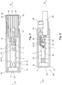
- a subassembly 1 for a sensor (not shown) is shown, which has a circuit board 2, to which a coil system 4 is attached at a first end 3 and an extension section 6 is attached at an opposite second end 5.
- the circuit board 2 is thus arranged between the coil system 4 and the extension section 6.
- the circuit board 2 is only shown schematically and has various electronic components 7 to 10, 28 and an arrangement 23 comprising three connection elements 11, 12, 13 for cables.
- the reference number 28 designates a light source for optically signaling the operating and/or switching states of a sensor, whereby this light source 28 can be a display LED. It goes without saying that more than just one light source can also be provided on the circuit board 2. For example, it is possible for four light sources to be arranged on the circuit board 2.
- a separation point 22 is provided between the extension section 6 and the circuit board 2, which enables the extension section 2 to be easily separated, i.e. removed, from the circuit board 2.
- the extension section 6 is divided in the longitudinal direction 18 into several preferably identical sections 14 to 17. Between each section 14 to 17, a separation point 19 to 21 is provided, which enables the extension section to be easily separated from the adjacent section.
- These separation points 19 to 22 have a defined, preferably the same, distance from one another.
- Each section also comprises an arrangement 24 to 27 of at least one connection element for at least one cable.
- Each arrangement 24 to 27 of sections 14 to 17 comprises three connection elements, whereby these connection elements of the arrangements 24 to 27 are not provided with reference numbers.
- Four cables 29 to 32 are attached to the arrangement 27 with its three connection elements. The cables are led to a plug or a cable connection. Such a plug or cable connection is in the Figure 1 However, these elements are not visible because they are part of the finished sensor, which Figure 1 but is not shown.
- the holes 34, 35 can also be replaced by notches. It is also possible for the separation points 19 to 22 to have both notches and holes. Instead of these notches or holes, a milling can also be provided. be provided.
- the at least one bore and/or the at least one notch can be arranged on a milled recess that runs along the transverse direction 33 of the extension section 6. This makes cutting through the corresponding separation point 19 to 22 particularly easy.
- the extension section 6 shown can, for example, have a length of 20 mm, whereby the sections 14 to 17 each have a length of 5 mm. By cutting off one of the sections 14 to 17, the subassembly 1 can be shortened by 5 mm each. If the subassembly 1 is to be shortened by 20 mm, the entire extension section 6 must be cut off from the circuit board 2.
- extension section 6 can also be larger or smaller than 20 mm.
- each section of the extension section 6 can be made smaller, so that the extension section 6 has more than just four sections. This and the variation in the length of the extension section make it possible to cover a wide variety of sensor lengths. In this case, a separation point for easy cutting is also provided between the section of the extension section directly adjacent to the circuit board 2 and between every other section of the extension section.
- each section also includes an arrangement with at least one connection element for at least one cable.
- extension section has fewer than four sections, which of course limits the possibility of variation with regard to different sensor lengths. It is therefore advantageous if the extension section has as many sections as possible that are connected to one another via separation points.
- the extension section has a length such that the subassembly can be installed in a sensor with the greatest length without shortening the extension section and in a sensor with the shortest length after removing the extension section.
- the subassembly consisting of the circuit board and the coil system, has a standardized size that can be installed in a sensor with the shortest length without machining.
- the subassembly has the extension section, which can be adapted to the desired sensor length by shortening the extension section.
- FIG 2 is a variant 40 of the Figure 1 Since this subassembly 40 can only be shortened by the construction of the separation points 19 to 22 for the subassembly 1 to Figure 1 , the reference numbers have essentially been retained. For the sake of clarity, however, only some elements of subassembly 40 are provided with reference numbers.
- the subassembly 40 in turn has the circuit board 2, which is arranged between the coil system 4 and the extension section 6.
- the extension section 6 consists of the four sections 14 to 17, wherein several cables 29 to 32 are attached to the arrangement 27 with the three connection elements of the last section 17.
- the separation points 19 to 22 are designed as milled recesses 41 to 45, with a bore 46 to 49 provided in the middle of each milled recess 41 to 45.
- the bores 46 to 49 are thus located in the corresponding milled recess 41 to 45.
- the combination of a milled recess 41 to 45 with a bore 46 to 49 makes cutting through the corresponding separation point 19 to 22 particularly easy.
- holes adjacent to one another can of course also be provided in the milled recesses 41 to 45 in the transverse direction 33 of the extension section 6.
- the holes can also optionally be replaced by other means, such as notches.
- Figure 3 shows a sensor 50 with subassembly 1 according to Figure 1 .
- the subassembly 1 is completely located in a housing 51 of the sensor 50, the housing 51 being closed by a cap 53 at a first end 52 of the sensor 50, where the coil system 4 is located.
- the subassembly 1 is completely surrounded by potting compound, which in the Figure 3 but is not shown.
- the subassembly 1 is to be installed in a sensor with a shorter length, this is also possible because some of the sections or even all of the sections, i.e. the entire extension section 6, can be separated.
- the cables 29 to 32 are led to a cable connection 36 of the sensor 50.
- the structure of such a cable connection 36 is known and is arranged at a second end 54 opposite the first end 52 of the sensor 50.
- the second end 54 is closed by a closure cap 37 and additionally sealed by a seal 38.
- the seal 38 can be designed as an O-ring.
- the cable connection 36 is additionally fixed in the sensor 50 by a holder 39.
- Figure 4 is a sensor 60 with the subassembly 1 according to Figure 1 shown.
- the subassembly 1 in turn consists of the coil system 4, the circuit board 2 arranged thereon and the extension section 6 adjoining the circuit board 2.
- the subassembly 1 is surrounded by a potting compound (not shown). This potting compound is in turn enclosed by the housing 51 together with the subassembly 1 in the longitudinal direction 18 and is surrounded at the end 52 by the cap 53, which closes the sensor 60 at this end 52.
- the extension section 6 was shortened by one section, namely section 17 (see Figure 1 ), so that the cables 29 to 32 are attached to the arrangement 26 with its three connection elements (without reference numbers) of the section 16.
- section 17 By removing, ie by cutting off, the section 17, not only the extension section 6 but the entire subassembly 1 has been shortened, so that the subassembly 1 now has a shorter length and is thus installed in a sensor 60 which has a shorter length than the sensor 50.
- the cables 29 to 32 are in turn led to the cable connection 36 of the sensor 60, wherein the cable connection 36 is accommodated at the second end 54 of the sensor 60.
- a sensor 70 is shown with the subassembly 1, in which the entire extension section 6 has been removed.
- the separation of this extension section 6 was achieved by cutting at the separation point 22, which lies between the extension section 6 and the circuit board 2 (compare Figure 1 ), is carried out.
- the shortening of the subassembly 1 by removing the extension section 6 is preferably carried out with a web separator (not shown) because this does not produce any dust or smoke. Because the extension section 6 can be easily separated due to the separation point 22, the separation can be excellently integrated into the manufacturing process of the sensor 70 and can even be easily automated.
- the cable connection 36 is provided, into which the cables 29 to 32 are guided.
- Connector pins are not required because the distance between the corresponding subassemblies and the corresponding cable connections is very small. If it is nevertheless necessary to use connector pins for these sensors 50, 60, 70, these connector pins can have standard lengths because the distances between the subassembly and the cable connection for sensors of different lengths can only be bridged by adjusting the extension section or removing the extension section.
Landscapes
- Physics & Mathematics (AREA)
- General Physics & Mathematics (AREA)
- Fire Alarms (AREA)
Claims (6)
- Sous-ensemble (1, 40) pour un capteur (50, 60, 70), comportant un système de bobines (4) ainsi qu'une carte de circuit imprimé (2) disposée sur celui-ci, une section de prolongement (6) étant montée dans la direction longitudinale (18) sur la carte de circuit imprimé (2) de sorte que la carte de circuit imprimé (2) est disposée entre le système de bobines (4) et la section de prolongement (6), un point de sectionnement (22) étant prévu entre la section de prolongement (6) et la carte de circuit imprimé (2), et le point de sectionnement (22) permettant de séparer facilement la section de prolongement (6) de la carte de circuit imprimé (2), caractérisé en ce que la section de prolongement (6) comporte, le long de la direction longitudinale (18), plusieurs sections (14 à 17) disposées les unes derrière les autres, un point de sectionnement (19 à 21) étant respectivement prévu entre deux sections voisines (14 à 17) pour une séparation facile de la section de prolongement (6).
- Sous-ensemble pour un capteur selon la revendication 1, caractérisé en ce que les points de sectionnement (19 à 22) sont réalisés sous forme d'un fraisage (41 à 45) et/ou d'au moins une encoche et/ou d'au moins un alésage (34, 35, 46 à 49).
- Sous-ensemble pour un capteur selon la revendication 1, caractérisé en ce que chaque point de sectionnement (19 à 22) présente plusieurs alésages (34, 35) et/ou plusieurs encoches le long d'une direction transversale (33) de la section de prolongement (6) et avec un écartement défini les uns des autres.
- Sous-ensemble pour un capteur selon la revendication 2, caractérisé en ce que l'au moins un alésage (46 à 49) et/ou l'au moins une encoche sont disposés dans un fraisage (41 à 45), le fraisage (41 à 45) s'étendant le long d'une direction transversale (33) de la section de prolongement (6).
- Sous-ensemble pour un capteur selon la revendication 1, caractérisé en ce que chaque section (14 à 17) comporte un agencement (23 à 27) comprenant au moins un élément de connexion pour des câbles (29 à 32).
- Capteur (50, 60, 70) comportant le sous-ensemble selon les revendications 1 à 5.
Priority Applications (1)
| Application Number | Priority Date | Filing Date | Title |
|---|---|---|---|
| EP20210352.9A EP4006496B1 (fr) | 2020-11-27 | 2020-11-27 | Sous-ensemble pour un capteur |
Applications Claiming Priority (1)
| Application Number | Priority Date | Filing Date | Title |
|---|---|---|---|
| EP20210352.9A EP4006496B1 (fr) | 2020-11-27 | 2020-11-27 | Sous-ensemble pour un capteur |
Publications (3)
| Publication Number | Publication Date |
|---|---|
| EP4006496A1 EP4006496A1 (fr) | 2022-06-01 |
| EP4006496B1 true EP4006496B1 (fr) | 2025-01-29 |
| EP4006496C0 EP4006496C0 (fr) | 2025-01-29 |
Family
ID=73642692
Family Applications (1)
| Application Number | Title | Priority Date | Filing Date |
|---|---|---|---|
| EP20210352.9A Active EP4006496B1 (fr) | 2020-11-27 | 2020-11-27 | Sous-ensemble pour un capteur |
Country Status (1)
| Country | Link |
|---|---|
| EP (1) | EP4006496B1 (fr) |
Family Cites Families (4)
| Publication number | Priority date | Publication date | Assignee | Title |
|---|---|---|---|---|
| DE3321666A1 (de) * | 1983-06-15 | 1984-12-20 | Siemens AG, 1000 Berlin und 8000 München | Anordnung zum verbinden von schaltungsplatinen |
| US5588202A (en) * | 1995-03-17 | 1996-12-31 | Honeywell Inc. | Method for manufacturing an overmolded sensor |
| DE19712879A1 (de) * | 1997-03-27 | 1998-10-01 | Turck Werner Kg | Verfahren zum Herstellen einer Schaltung und zugehöriges Nutzen |
| DE102008006746A1 (de) | 2008-01-30 | 2009-08-06 | Pepperl + Fuchs Gmbh | Sensor und Verfahren zu dessen Herstellung |
-
2020
- 2020-11-27 EP EP20210352.9A patent/EP4006496B1/fr active Active
Also Published As
| Publication number | Publication date |
|---|---|
| EP4006496A1 (fr) | 2022-06-01 |
| EP4006496C0 (fr) | 2025-01-29 |
Similar Documents
| Publication | Publication Date | Title |
|---|---|---|
| DE69816236T2 (de) | Schnittstellenvorrichtung zwischen Teilen einer Anlage | |
| EP2728982B1 (fr) | Composant à plaquettes pour un appareil de commande, appareil de commande pour un véhicule automobile et agencement de traitement du signal | |
| DE102011087328B4 (de) | Verfahren zur Herstellung einer umspritzten Sensorbaugruppe sowie eine Sensorbaugruppe | |
| EP0015309A1 (fr) | Dispositif de pression d'un guide d'onde optique contre un élément photoélectrique | |
| DE102009055859A1 (de) | Verfahren zum Kontaktieren einer beidseitig mit elektrischen Kontakten versehenen Leiterplatte und solche Leiterplatte | |
| EP2023442A2 (fr) | Platine en plusieurs parties | |
| DE102016125350A1 (de) | Verbindungselement und Transmittergehäuse mit darin eingesetzten Verbindungselement | |
| DE102016121047A1 (de) | Beleuchtungseinrichtung für ein fahrzeug sowie herstellungsverfahren für eine beleuchtungseinrichtung | |
| DE102013209296A1 (de) | Elektronisches Modul, insbesondere Steuergerät für ein Fahrzeug und Verfahren zu dessen Herstellung | |
| EP0740082A1 (fr) | Dispositif électrique modulaire pour un assemblage de bloc de vannes | |
| EP4006496B1 (fr) | Sous-ensemble pour un capteur | |
| DE3910913C2 (de) | Pneumatische oder hydraulische Ventileinheit | |
| EP2614691B1 (fr) | Carte de circuit imprimé pour le montage de corps lumineux | |
| DE3717743C2 (de) | Verfahren zur Herstellung elektrischer Geräte und nach diesem Verfahren hergestellte Geräte | |
| DE60121820T2 (de) | Verfahren zur Herstellung integrierter Schaltungen mit verbesserten Leiterbahnen in sogenannter "Sägebügel"-Form | |
| DE102011076377A1 (de) | Elektrische Reihenklemmenanordnung | |
| DE102017202329A1 (de) | Multilayer-Leiterplatte sowie elektronische Anordnung mit einer solchen | |
| DE102004014034A1 (de) | Leiterplatte mit wenigstens einer Anschlußbohrung für einen Anschlußdraht bzw. -Pin eines bedrahteten elektronischen Bauteils | |
| DE3806792A1 (de) | Vorrichtung zum pruefen von leiterplatten | |
| DE19943388B4 (de) | Vorrichtung zum Prüfen von Leiterplatten | |
| DE102015220794A1 (de) | Trägerelement für ein Lichtmodul einer Kraftfahrzeugbeleuchtungseinrichtung | |
| DE102019217344A1 (de) | Beleuchtungsmodule mit einem schaltungsträger und lichtquellen | |
| EP0982806B1 (fr) | Connecteur avec éléments de contact adapté à être monté sur une plaquette à circuits imprimés | |
| EP4351291A1 (fr) | Agencement de composants pour une électronique de puissance et procédé de fourniture d'un agencement de composants pour une électronique de puissance | |
| AT18098U1 (de) | Leiterplatte umfassend Öffnung zum Anordnen einer weiteren Leiterplatte auf der Leiterplatte |
Legal Events
| Date | Code | Title | Description |
|---|---|---|---|
| PUAI | Public reference made under article 153(3) epc to a published international application that has entered the european phase |
Free format text: ORIGINAL CODE: 0009012 |
|
| STAA | Information on the status of an ep patent application or granted ep patent |
Free format text: STATUS: THE APPLICATION HAS BEEN PUBLISHED |
|
| AK | Designated contracting states |
Kind code of ref document: A1 Designated state(s): AL AT BE BG CH CY CZ DE DK EE ES FI FR GB GR HR HU IE IS IT LI LT LU LV MC MK MT NL NO PL PT RO RS SE SI SK SM TR |
|
| STAA | Information on the status of an ep patent application or granted ep patent |
Free format text: STATUS: REQUEST FOR EXAMINATION WAS MADE |
|
| 17P | Request for examination filed |
Effective date: 20220615 |
|
| RBV | Designated contracting states (corrected) |
Designated state(s): AL AT BE BG CH CY CZ DE DK EE ES FI FR GB GR HR HU IE IS IT LI LT LU LV MC MK MT NL NO PL PT RO RS SE SI SK SM TR |
|
| STAA | Information on the status of an ep patent application or granted ep patent |
Free format text: STATUS: EXAMINATION IS IN PROGRESS |
|
| 17Q | First examination report despatched |
Effective date: 20230310 |
|
| GRAP | Despatch of communication of intention to grant a patent |
Free format text: ORIGINAL CODE: EPIDOSNIGR1 |
|
| STAA | Information on the status of an ep patent application or granted ep patent |
Free format text: STATUS: GRANT OF PATENT IS INTENDED |
|
| INTG | Intention to grant announced |
Effective date: 20241016 |
|
| RIN1 | Information on inventor provided before grant (corrected) |
Inventor name: DREBES, PATRICK Inventor name: GEIGER, THOMAS Inventor name: ELTER, JOHANN |
|
| GRAS | Grant fee paid |
Free format text: ORIGINAL CODE: EPIDOSNIGR3 |
|
| GRAA | (expected) grant |
Free format text: ORIGINAL CODE: 0009210 |
|
| STAA | Information on the status of an ep patent application or granted ep patent |
Free format text: STATUS: THE PATENT HAS BEEN GRANTED |
|
| AK | Designated contracting states |
Kind code of ref document: B1 Designated state(s): AL AT BE BG CH CY CZ DE DK EE ES FI FR GB GR HR HU IE IS IT LI LT LU LV MC MK MT NL NO PL PT RO RS SE SI SK SM TR |
|
| REG | Reference to a national code |
Ref country code: GB Ref legal event code: FG4D Free format text: NOT ENGLISH |
|
| REG | Reference to a national code |
Ref country code: CH Ref legal event code: EP |
|
| REG | Reference to a national code |
Ref country code: DE Ref legal event code: R096 Ref document number: 502020010303 Country of ref document: DE |
|
| REG | Reference to a national code |
Ref country code: IE Ref legal event code: FG4D Free format text: LANGUAGE OF EP DOCUMENT: GERMAN |
|
| U01 | Request for unitary effect filed |
Effective date: 20250221 |
|
| U07 | Unitary effect registered |
Designated state(s): AT BE BG DE DK EE FI FR IT LT LU LV MT NL PT RO SE SI Effective date: 20250228 |
|
| PG25 | Lapsed in a contracting state [announced via postgrant information from national office to epo] |
Ref country code: RS Free format text: LAPSE BECAUSE OF FAILURE TO SUBMIT A TRANSLATION OF THE DESCRIPTION OR TO PAY THE FEE WITHIN THE PRESCRIBED TIME-LIMIT Effective date: 20250429 |
|
| PG25 | Lapsed in a contracting state [announced via postgrant information from national office to epo] |
Ref country code: PL Free format text: LAPSE BECAUSE OF FAILURE TO SUBMIT A TRANSLATION OF THE DESCRIPTION OR TO PAY THE FEE WITHIN THE PRESCRIBED TIME-LIMIT Effective date: 20250129 |
|
| PG25 | Lapsed in a contracting state [announced via postgrant information from national office to epo] |
Ref country code: ES Free format text: LAPSE BECAUSE OF FAILURE TO SUBMIT A TRANSLATION OF THE DESCRIPTION OR TO PAY THE FEE WITHIN THE PRESCRIBED TIME-LIMIT Effective date: 20250129 |
|
| PG25 | Lapsed in a contracting state [announced via postgrant information from national office to epo] |
Ref country code: IS Free format text: LAPSE BECAUSE OF FAILURE TO SUBMIT A TRANSLATION OF THE DESCRIPTION OR TO PAY THE FEE WITHIN THE PRESCRIBED TIME-LIMIT Effective date: 20250529 Ref country code: NO Free format text: LAPSE BECAUSE OF FAILURE TO SUBMIT A TRANSLATION OF THE DESCRIPTION OR TO PAY THE FEE WITHIN THE PRESCRIBED TIME-LIMIT Effective date: 20250429 |
|
| PG25 | Lapsed in a contracting state [announced via postgrant information from national office to epo] |
Ref country code: HR Free format text: LAPSE BECAUSE OF FAILURE TO SUBMIT A TRANSLATION OF THE DESCRIPTION OR TO PAY THE FEE WITHIN THE PRESCRIBED TIME-LIMIT Effective date: 20250129 |
|
| PG25 | Lapsed in a contracting state [announced via postgrant information from national office to epo] |
Ref country code: GR Free format text: LAPSE BECAUSE OF FAILURE TO SUBMIT A TRANSLATION OF THE DESCRIPTION OR TO PAY THE FEE WITHIN THE PRESCRIBED TIME-LIMIT Effective date: 20250430 |
|
| PG25 | Lapsed in a contracting state [announced via postgrant information from national office to epo] |
Ref country code: SM Free format text: LAPSE BECAUSE OF FAILURE TO SUBMIT A TRANSLATION OF THE DESCRIPTION OR TO PAY THE FEE WITHIN THE PRESCRIBED TIME-LIMIT Effective date: 20250129 |
|
| PG25 | Lapsed in a contracting state [announced via postgrant information from national office to epo] |
Ref country code: SK Free format text: LAPSE BECAUSE OF FAILURE TO SUBMIT A TRANSLATION OF THE DESCRIPTION OR TO PAY THE FEE WITHIN THE PRESCRIBED TIME-LIMIT Effective date: 20250129 |
|
| REG | Reference to a national code |
Ref country code: CH Ref legal event code: U11 Free format text: ST27 STATUS EVENT CODE: U-0-0-U10-U11 (AS PROVIDED BY THE NATIONAL OFFICE) Effective date: 20251201 |
|
| PLBE | No opposition filed within time limit |
Free format text: ORIGINAL CODE: 0009261 |
|
| STAA | Information on the status of an ep patent application or granted ep patent |
Free format text: STATUS: NO OPPOSITION FILED WITHIN TIME LIMIT |
|
| U20 | Renewal fee for the european patent with unitary effect paid |
Year of fee payment: 6 Effective date: 20251117 |
|
| 26N | No opposition filed |
Effective date: 20251030 |
|
| PGFP | Annual fee paid to national office [announced via postgrant information from national office to epo] |
Ref country code: CH Payment date: 20251201 Year of fee payment: 6 |
|
| PGFP | Annual fee paid to national office [announced via postgrant information from national office to epo] |
Ref country code: CZ Payment date: 20251118 Year of fee payment: 6 |