EP4006561B1 - Procédé de connexion de tête d'essai - Google Patents
Procédé de connexion de tête d'essai Download PDFInfo
- Publication number
- EP4006561B1 EP4006561B1 EP21208608.6A EP21208608A EP4006561B1 EP 4006561 B1 EP4006561 B1 EP 4006561B1 EP 21208608 A EP21208608 A EP 21208608A EP 4006561 B1 EP4006561 B1 EP 4006561B1
- Authority
- EP
- European Patent Office
- Prior art keywords
- test head
- test
- load board
- test fixture
- connection method
- Prior art date
- Legal status (The legal status is an assumption and is not a legal conclusion. Google has not performed a legal analysis and makes no representation as to the accuracy of the status listed.)
- Active
Links
Images



Classifications
-
- G—PHYSICS
- G01—MEASURING; TESTING
- G01R—MEASURING ELECTRIC VARIABLES; MEASURING MAGNETIC VARIABLES
- G01R31/00—Arrangements for testing electric properties; Arrangements for locating electric faults; Arrangements for electrical testing characterised by what is being tested not provided for elsewhere
- G01R31/28—Testing of electronic circuits, e.g. by signal tracer
- G01R31/2851—Testing of integrated circuits [IC]
- G01R31/2886—Features relating to contacting the IC under test, e.g. probe heads; chucks
- G01R31/2887—Features relating to contacting the IC under test, e.g. probe heads; chucks involving moving the probe head or the IC under test; docking stations
-
- H—ELECTRICITY
- H10—SEMICONDUCTOR DEVICES; ELECTRIC SOLID-STATE DEVICES NOT OTHERWISE PROVIDED FOR
- H10P—GENERIC PROCESSES OR APPARATUS FOR THE MANUFACTURE OR TREATMENT OF DEVICES COVERED BY CLASS H10
- H10P74/00—Testing or measuring during manufacture or treatment of wafers, substrates or devices
- H10P74/20—Testing or measuring during manufacture or treatment of wafers, substrates or devices characterised by the properties tested or measured, e.g. structural or electrical properties
- H10P74/203—Structural properties, e.g. testing or measuring thicknesses, line widths, warpage, bond strengths or physical defects
-
- G—PHYSICS
- G01—MEASURING; TESTING
- G01R—MEASURING ELECTRIC VARIABLES; MEASURING MAGNETIC VARIABLES
- G01R1/00—Details of instruments or arrangements of the types included in groups G01R5/00 - G01R13/00 and G01R31/00
- G01R1/02—General constructional details
- G01R1/06—Measuring leads; Measuring probes
- G01R1/067—Measuring probes
- G01R1/073—Multiple probes
- G01R1/07307—Multiple probes with individual probe elements, e.g. needles, cantilever beams or bump contacts, fixed in relation to each other, e.g. bed of nails fixture or probe card
- G01R1/07342—Multiple probes with individual probe elements, e.g. needles, cantilever beams or bump contacts, fixed in relation to each other, e.g. bed of nails fixture or probe card the body of the probe being at an angle other than perpendicular to test object, e.g. probe card
-
- G—PHYSICS
- G01—MEASURING; TESTING
- G01R—MEASURING ELECTRIC VARIABLES; MEASURING MAGNETIC VARIABLES
- G01R31/00—Arrangements for testing electric properties; Arrangements for locating electric faults; Arrangements for electrical testing characterised by what is being tested not provided for elsewhere
- G01R31/28—Testing of electronic circuits, e.g. by signal tracer
- G01R31/2851—Testing of integrated circuits [IC]
- G01R31/2855—Environmental, reliability or burn-in testing
- G01R31/286—External aspects, e.g. related to chambers, contacting devices or handlers
- G01R31/2863—Contacting devices, e.g. sockets, burn-in boards or mounting fixtures
-
- G—PHYSICS
- G01—MEASURING; TESTING
- G01R—MEASURING ELECTRIC VARIABLES; MEASURING MAGNETIC VARIABLES
- G01R31/00—Arrangements for testing electric properties; Arrangements for locating electric faults; Arrangements for electrical testing characterised by what is being tested not provided for elsewhere
- G01R31/28—Testing of electronic circuits, e.g. by signal tracer
- G01R31/2851—Testing of integrated circuits [IC]
- G01R31/2886—Features relating to contacting the IC under test, e.g. probe heads; chucks
- G01R31/2889—Interfaces, e.g. between probe and tester
-
- H—ELECTRICITY
- H10—SEMICONDUCTOR DEVICES; ELECTRIC SOLID-STATE DEVICES NOT OTHERWISE PROVIDED FOR
- H10P—GENERIC PROCESSES OR APPARATUS FOR THE MANUFACTURE OR TREATMENT OF DEVICES COVERED BY CLASS H10
- H10P72/00—Handling or holding of wafers, substrates or devices during manufacture or treatment thereof
- H10P72/70—Handling or holding of wafers, substrates or devices during manufacture or treatment thereof for supporting or gripping
- H10P72/78—Handling or holding of wafers, substrates or devices during manufacture or treatment thereof for supporting or gripping using vacuum or suction, e.g. Bernoulli chucks
-
- G—PHYSICS
- G01—MEASURING; TESTING
- G01R—MEASURING ELECTRIC VARIABLES; MEASURING MAGNETIC VARIABLES
- G01R31/00—Arrangements for testing electric properties; Arrangements for locating electric faults; Arrangements for electrical testing characterised by what is being tested not provided for elsewhere
- G01R31/28—Testing of electronic circuits, e.g. by signal tracer
- G01R31/2851—Testing of integrated circuits [IC]
- G01R31/2855—Environmental, reliability or burn-in testing
- G01R31/286—External aspects, e.g. related to chambers, contacting devices or handlers
- G01R31/2868—Complete testing stations; systems; procedures; software aspects
Definitions
- the present invention pertains to a method for connecting a test head, more specifically to a method for connecting a test head and a probing machine by direct probing.
- the wafer In order to properly move and load a wafer, the wafer is usually placed in a probing machine during test procedures and tested by a test head.
- the test head may have many probe cards which are electrically connected to a load board, and then the load board is electrically connected to the wafer.
- the load board does not directly contact the wafer.
- the load board should be connected to a pogo tower, and then the pogo tower contacts the wafer. Since the pogo tower and the load board need to be placed between the test head and the probing machine, it is obvious that the test head will be away from the probing machine.
- the pogo tower and the load board need to be placed between the test head and the probing machine, it is obvious that the test head will be away from the probing machine.
- there is the pogo tower disposed between the load board and the wafer which makes the signal transmission path much longer, and there will be more interference and greater signal attenuation.
- the test head and the probing machine are fixed together by mechanical means to fix the relative position of the load board and the pogo tower, and then the load board can be electrically connected to the wafer through the pogo tower.
- the traditional probing machine is designed to have the pogo tower, and the load board and the wafer are not close to each other. In other words, even though the pogo tower is removed, the load board is still away from the wafer by a considerable distance. And, if the load board is still locked to the test head, there is a problem that the load board cannot touch the wafer for sure. Accordingly, the industry needs a new method for connecting the test head, so that the test head and the probing machine can be adjusted to operate in the direct docking mode.
- US 9 903 885 B1 discloses a traditional tester with direct docking using a load board, and a test fixture, where the load board is accommodated, disposed on the test head.
- US 2003/201764 A1 and US 6 166 552 A also disclose traditional testers.
- the present invention provides a test head connection method, which can be used to connect a test head to a probing machine.
- the load board is set on the probing machine instead of the test head, and when the test head contacts the load board, the load board can be sucked tightly by the vacuum function of the test head to increase the stability between the test head and the probing machine.
- the present invention discloses a test head connection method comprising the following steps: disposing a load board and a test fixture between the test head and a probing machine; activating a vacuum function of the test head; moving the test head to align the test fixture; moving the test head until touching the load board in the test fixture; fixing the test head and the test fixture by at least one engaging member.
- the test fixture is disposed in the probing machine, the test fixture is used to accommodate the load board, and the load board is configured to connect a wafer by direct probing.
- the test fixture defines a first upper surface, the first upper surface defines a first accommodating space, and the first accommodating space may be used for accommodating the load board.
- the load board and the first upper surface may form a coplanar surface.
- the test head connection method may further comprise: providing a fixing plate detachably locked to the probing machine. Wherein a second upper surface of the fixing plate defines a second accommodating space, and the second accommodating space may be used for accommodating the test fixture.
- the first upper surface and the second upper surface are not coplanar, and the test fixture is detachably locked in the second accommodating space of the fixing plate.
- the load board may be detachably locked in the first accommodating space.
- the step of moving the test head to align the test fixture may further comprise: providing an alignment member, disposed on the test fixture, to guide the test head to align with the test fixture.
- the test head may contact an upper surface of the load board, and the test fixture may contact a lower surface of the load board.
- the upper surface of the load board defines at least a vacuum area, and the vacuum area may be surrounded by a metal strip.
- the test head connection method provided by the present invention can be used to connect the test head to the probing machine, and the vacuum function of the test head can be used to suck the load board tightly, so that the load board can be pressed toward the test head more efficiently.
- the load board is arranged in the probing machine, the stability between the test head and the probing machine can also be increased.
- the base body 12 is approximately cube-shaped, and the width W2 of the base body 12, in the same axial direction, is slightly narrower than the width W1 of the housing 10.
- the present embodiment does not limit the numerical or proportional value between the width W1 and the width W2. Since the base body 12 protrudes from the bottom surface 10a, persona having ordinary skill in the art can understand that the bottom surface 10a and the test surface 12a will not be coplanar. In one example, the test surface 12a is closer, in FIG. 1 , to the probing machine 2 than the bottom surface 10a.
- the housing 10 can be provided with various components for the electrical testing and the vacuum function.
- the housing 10 can be provided with multiple probe cards, and each probe card can have more than one probe set. The probe sets can protrude from the test surface 12a through an opening 120 on the test surface 12a.
- each opening 120 on the test surface 12a does not necessarily correspond to one of the probe cards. For example, there may be only a few probe cards inside the housing 10, so that some openings 120 may not have protruding probe sets. Taking the example shown in FIG. 2 and FIG. 3 , the openings 120 on the test surface 12a can be divided into two rows, and the number of the openings 120 in each row is the same. This embodiment does not limit the number of the openings 120 on the test surface 12a.
- the openings in each row can be surrounded by a sealing strip 122 in appearance. In practice, the area surrounded by the sealing strip 122 is provided with one or more through holes for vacuum suction, that is, the area surrounded by the sealing strip 122 is related to the vacuum function of the test head 1, which will be described later.
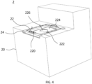
- the fixing plate 24 is first disposed on the housing 20, and the test fixture 22 is then fixed to the housing 20 by the fixing plate 24.
- the test fixture 22 is detachably locked to the fixing plate 24.
- the test fixture 22 can be fixed to the fixing plate 24 with screws, which is not limited in this embodiment.
- the test fixture 22 may be provided with an engaging member 220 and an alignment member 222, and the engaging member 220 and the engaging member 100 may structurally correspond to each other.
- the engaging member 100 may be a slot
- the engaging member 220 may be a short post which can be slid into the slot to be locked and fixed to each other.
- the alignment member 104 and the alignment member 222 can be used to align the test head 1 and the probing machine 2.
- the alignment member 104 may be a groove
- the alignment member 222 may be a column
- the alignment member 104 may accommodate the alignment member 222.
- This embodiment does not limit the shape of the alignment member 104 and the shape of the alignment member 222, as long as the shape of the alignment member 222 can correspond to the shape of the alignment member 104, it should be in the scope described in this embodiment.
- the engaging member 220 and the alignment member 222 can be set on the fixing plate 24.
- the fixing member 102 such as a handle
- the fixing member 102 may trigger a blocking structure (not shown in figures) which can prevent the engaging member 220 from exiting or detaching from the engaging member 100.
- This embodiment does not limit the means of the blocking structure.
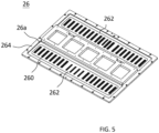
- FIG. 5 is a schematic diagram of a load board in accordance with an embodiment of the present invention.
- FIG. 6 is a schematic diagram of the load board and a fixing plate in accordance with an embodiment of the present invention.
- FIG. 6 shows that the test fixture 22 and the fixing plate 24 are separable.
- the test fixture 22 has an upper surface 22a (first upper surface), and the upper surface 22a defines an accommodating space 224 (first accommodating space).
- the test fixture 22 has a basin-shaped in appearance.
- the edge of the basin-shaped test fixture 22 can be locked to the fixing plate 24, and the bottom of the basin-shaped test fixture 22 can be accommodated in the fixing plate 24.
- the test fixture 22 is locked to the upper surface 24a, so the edge of the test fixture 22 is higher than the bottom of the test fixture 22. That is, the edge of the test fixture 22 is closer to the test surface 12a of the test head 1 than the bottom of the test fixture 22.
- the bottom of the test fixture 22 is the upper surface 22a (first upper surface). When the test fixture 22 is contained in the fixing plate 24, the upper surface 22a and the upper surface 24a are not coplanar.
- the upper surface 26a of the load board 26 which is adjacent to the test head 1 (shown in FIG. 5 ) may have a plurality of pads 260 and vacuum areas 262. Similar to the examples shown in FIG. 2 and FIG. 3 , the pads 260 on the load board 26 can also be divided into two rows, and each row of the pads 260 is located in one of the vacuum areas 262. In one example, the load board 26 is further provided with a metal strip 264 on the edge of the upper surface 26a.
- the metal strip 264 can be regarded as a rectangle in appearance and surround both of the vacuum areas 262. The present embodiment does not limit the position and shape of the metal strip 264.
- the metal strip 264 may not be arranged on the edge of the upper surface 26a, but on the edge of each vacuum area 262.
- the metal strip 264 can be regarded as two rectangles, each rectangle encloses one of the vacuum areas 262.
- the lower side of the load board 26 away from the test head 1 may have a plurality of probes (not shown) for connecting the wafer, and the probe can pass through the upper surface 22a through the slot 226 in the test fixture 22, and directly contact the wafer (not shown) disposed below, which will not be rep
- the load board 26 will also be pre-locked in the accommodating space 224 of the test fixture 22.
- the upper surface 26a of the load board 26 can be the same height (coplanar) with the upper surface 22a of the test fixture 22, or the top of the metal strip 264 located on the upper surface 26a can be the same height (coplanar) with the upper surface 22a of the test fixture 22, which is not limited in this embodiment.
- the load board 26 is locked in the accommodating space 224, at least a part of the load board 26 will be coplanar with the upper surface 22a.
- the base body 12 of the test head 1 is aligned with the test fixture 22, which also represents the openings 120 on the test surface 12a can be aligned with the pads 260 on the upper surface 26a since the load board 26 and the test fixture 22 do not move relatively to each other.
- the upper surface 26a of the load board 26 is used to contact the base body 12 of the test head 1, and the surface (for example, the lower side) of the load board 26 opposite to the upper surface 26a is used to contact the test fixture 22.
- the test head 1 and the probing machine 2 can perform the alignment procedures, such as aligning the alignment member 104 and the alignment member 222 with each other, and let the engaging member 220 fit or enter the engaging member 100.
- the user can pull the fixing element 102 on the test head 1 to lock the relative position of the engaging member 100 and the engaging member 240.
- the test head 1 has been fully connected or fixed to the probing machine 2.
- part of the base body 12 will be pushed into the recess, the basin-shaped structure, of the test fixture 22.
- the recess, the basin-shaped structure, of the test fixture 22 may be square in appearance and have a width W3 in an axial direction.
- the vacuum function of the test head 1 mentioned in this embodiment can be used for other purposes in addition to stabilizing the electrical connection between the probe sets and the pads 260.
- the test head 1 may be originally designed with the vacuum function, but it is not used to stabilize the electrical connection between the probe sets and the pads 260.
- the vacuum function may be designed to suck exhaust gas around the object under test or suck the replaced pogo tower, that is, a new application of the vacuum function is introduced in this embodiment.
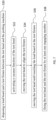
- FIG. 7 shows a flowchart of the test head connection method according to an embodiment of the present invention.
- step S30 the load board 26 and the test fixture 22 are arranged between the test head 1 and the probing machine 2.
- the test fixture 22 is set in the probing machine 2, and the test fixture 22 is used for accommodating the load board 26.
- step S32 the vacuum function of the test head 1 is activated, and in step S34, the test head 1 is moved to align the test fixture 22.
- step S36 the test head 1 is moved to contact the load board 26 in the test fixture 22.
- step S38 the engaging member 100 and the engaging member 220 are used to fix the test head 1 and the test fixture 22.
- the test head 1 and the probing machine 2 are connected in the direct probing connection, and the load board 26 can directly contact the wafer.
- the other steps of the test head connection method have been described in the previous embodiment, and this embodiment will not be repeated here.
- the test head connection method provided by the present invention can be used by the old probing machine. As long as the test fixture is replaced with a recessed basin-shaped structure, the old probing machine and the test head can be connected to each other in the direct docking connection. In this way, the problem of the long signal transmission path corresponding to the traditional pogo tower is solved.
- the present invention can also use the vacuum function of the test head can be used to suck the load board tightly, so that the load board can be pressed toward the test head more efficiently. Since the load board is arranged in the probing machine, the stability between the test head and the probing machine can also be increased.
Landscapes
- Engineering & Computer Science (AREA)
- Physics & Mathematics (AREA)
- General Physics & Mathematics (AREA)
- Computer Hardware Design (AREA)
- Microelectronics & Electronic Packaging (AREA)
- General Engineering & Computer Science (AREA)
- Environmental & Geological Engineering (AREA)
- Testing Or Measuring Of Semiconductors Or The Like (AREA)
- Tests Of Electronic Circuits (AREA)
- Cable Accessories (AREA)
- Magnetic Heads (AREA)
- Coupling Device And Connection With Printed Circuit (AREA)
- Testing Of Individual Semiconductor Devices (AREA)
Claims (10)
- Procédé de connexion de tête d'essai pour connecter une tête d'essai (1) et une machine de sondage (2), comprenant :la disposition d'un plateau de chargement (26) et d'un montage d'essai (22) entre la tête d'essai et la machine de sondage ;l'activation d'une fonction d'aspiration de la tête d'essai (1) ;le déplacement de la tête d'essai (1) pour aligner le montage d'essai ;le déplacement de la tête d'essai (1) jusqu'à ce qu'elle touche le plateau de chargement (26) dans le montage d'essai (22) ; etla fixation de la tête d'essai (1) et du montage d'essai (22) par au moins un élément d'engagement (100, 220) ;dans lequel le montage d'essai (22) est disposé dans la machine de sondage (2), et le montage d'essai (22) est utilisé pour accueillir le plateau de chargement (26) ;dans lequel le plateau de chargement (26) est configuré pour connecter une plaquette par sondage direct.
- Procédé de connexion de tête d'essai selon la revendication 1, dans lequel le montage d'essai définit une première surface supérieure (22a), la première surface supérieure définit un premier espace de logement (224), et le premier espace de logement est utilisé pour loger le plateau de chargement.
- Procédé de connexion de tête d'essai selon la revendication 2, dans lequel lorsque le plateau de chargement est logé dans le premier espace de logement, le plateau de chargement et la première surface supérieure forment une surface coplanaire.
- Procédé de connexion de tête d'essai selon la revendication 2, comprenant en outre : la fourniture d'une plaque de fixation (24) verrouillée de manière amovible à la machine de sondage ; une deuxième surface supérieure (24a) de la plaque de fixation définissant un deuxième espace de logement (240), et le deuxième espace de logement étant utilisé pour loger le montage d'essai.
- Procédé de connexion de tête d'essai selon la revendication 4, dans lequel la première surface supérieure et la deuxième surface supérieure ne sont pas coplanaires.
- Procédé de connexion de tête d'essai selon la revendication 4, dans lequel le montage d'essai est verrouillé de manière amovible dans le deuxième espace de logement de la plaque de fixation.
- Procédé de connexion de tête d'essai selon la revendication 2, dans lequel le plateau de chargement est verrouillé de manière amovible dans le premier espace de logement.
- Procédé de connexion de tête d'essai selon la revendication 1, dans lequel l'étape de déplacement de la tête d'essai pour aligner le montage d'essai comprend en outre :
la fourniture d'un élément d'alignement (222), disposé sur le montage d'essai, pour guider la tête d'essai afin de l'aligner avec le montage d'essai. - Procédé de connexion de tête d'essai selon la revendication 1, dans lequel la tête d'essai est en contact avec une surface supérieure (26a) du plateau de chargement, et le montage d'essai est en contact avec une surface inférieure du plateau de chargement.
- Procédé de connexion de tête d'essai selon la revendication 9, dans lequel la surface supérieure du plateau de chargement définit au moins une zone d'aspiration (262), et la zone d'aspiration est entourée d'une bande métallique (264).
Applications Claiming Priority (1)
| Application Number | Priority Date | Filing Date | Title |
|---|---|---|---|
| TW109140284A TWI771805B (zh) | 2020-11-18 | 2020-11-18 | 探針頭連接方法 |
Publications (3)
| Publication Number | Publication Date |
|---|---|
| EP4006561A1 EP4006561A1 (fr) | 2022-06-01 |
| EP4006561C0 EP4006561C0 (fr) | 2025-03-05 |
| EP4006561B1 true EP4006561B1 (fr) | 2025-03-05 |
Family
ID=78676394
Family Applications (1)
| Application Number | Title | Priority Date | Filing Date |
|---|---|---|---|
| EP21208608.6A Active EP4006561B1 (fr) | 2020-11-18 | 2021-11-16 | Procédé de connexion de tête d'essai |
Country Status (4)
| Country | Link |
|---|---|
| US (1) | US11908753B2 (fr) |
| EP (1) | EP4006561B1 (fr) |
| JP (1) | JP7297034B2 (fr) |
| TW (1) | TWI771805B (fr) |
Families Citing this family (1)
| Publication number | Priority date | Publication date | Assignee | Title |
|---|---|---|---|---|
| TWI797824B (zh) * | 2021-09-17 | 2023-04-01 | 致茂電子股份有限公司 | 壓測頭之快速拆裝組件及具備該組件之電子元件測試設備 |
Family Cites Families (11)
| Publication number | Priority date | Publication date | Assignee | Title |
|---|---|---|---|---|
| US6166552A (en) * | 1996-06-10 | 2000-12-26 | Motorola Inc. | Method and apparatus for testing a semiconductor wafer |
| US7382142B2 (en) | 2000-05-23 | 2008-06-03 | Nanonexus, Inc. | High density interconnect system having rapid fabrication cycle |
| JP2002076073A (ja) | 2000-08-28 | 2002-03-15 | Nec Corp | ウェハの検査装置及びウェハの検査方法 |
| US6794889B2 (en) * | 2002-04-26 | 2004-09-21 | Agilent Technologies, Inc. | Unified apparatus and method to assure probe card-to-wafer parallelism in semiconductor automatic wafer test, probe card measurement systems, and probe card manufacturing |
| WO2007057944A1 (fr) * | 2005-11-15 | 2007-05-24 | Advantest Corporation | Dispositif d'essai de composants electroniques et procede de chargement de panneau de performance sur ce dispositif |
| SG180056A1 (en) * | 2010-10-28 | 2012-05-30 | Sony Corp | An antenna |
| US9134357B1 (en) * | 2011-03-25 | 2015-09-15 | Maxim Integrated, Inc. | Universal direct docking at probe test |
| JP5926954B2 (ja) | 2011-12-28 | 2016-05-25 | 株式会社日本マイクロニクス | プローブカードの平行確認方法及び平行確認装置並びにプローブカード及びテストヘッド |
| TWI447414B (zh) * | 2012-06-07 | 2014-08-01 | 矽品精密工業股份有限公司 | 測試裝置及測試方法 |
| JP6895772B2 (ja) * | 2017-03-07 | 2021-06-30 | 東京エレクトロン株式会社 | 検査装置およびコンタクト方法 |
| JP7267058B2 (ja) | 2019-03-26 | 2023-05-01 | 東京エレクトロン株式会社 | 検査装置 |
-
2020
- 2020-11-18 TW TW109140284A patent/TWI771805B/zh active
-
2021
- 2021-11-06 US US17/520,631 patent/US11908753B2/en active Active
- 2021-11-16 EP EP21208608.6A patent/EP4006561B1/fr active Active
- 2021-11-16 JP JP2021186106A patent/JP7297034B2/ja active Active
Also Published As
| Publication number | Publication date |
|---|---|
| EP4006561A1 (fr) | 2022-06-01 |
| TW202221334A (zh) | 2022-06-01 |
| EP4006561C0 (fr) | 2025-03-05 |
| JP7297034B2 (ja) | 2023-06-23 |
| US20220068726A1 (en) | 2022-03-03 |
| JP2022080881A (ja) | 2022-05-30 |
| US11908753B2 (en) | 2024-02-20 |
| TWI771805B (zh) | 2022-07-21 |
Similar Documents
| Publication | Publication Date | Title |
|---|---|---|
| KR101859388B1 (ko) | 수직 프로브 카드 | |
| US20160231355A1 (en) | Semiconductor chip test device | |
| EP4006561B1 (fr) | Procédé de connexion de tête d'essai | |
| JP2000182741A (ja) | 電気部品用ソケット | |
| KR20130005874A (ko) | 반도체 패키지 테스트용 소켓 | |
| KR20060087125A (ko) | 반도체 소자 테스트용 소켓 어셈블리 | |
| KR102012439B1 (ko) | 반도체 칩 테스트 소켓 | |
| TW202119035A (zh) | Ic檢查用插座 | |
| JP2002365310A (ja) | 垂直型プローブカード | |
| CN114518472B (zh) | 探针头连接方法 | |
| KR100773194B1 (ko) | 볼 그리드 어레이 패키지용 소켓 | |
| KR102673746B1 (ko) | 프로버의 콤보 척 | |
| JP2020161631A (ja) | 検査装置 | |
| KR20230103390A (ko) | 칩 레벨 테스트용 웨이퍼 및 이를 이용하여 테스트하는 방법 | |
| KR101332656B1 (ko) | 반도체 모듈 테스트용 반도체칩 접속 디바이스 | |
| KR20220091170A (ko) | 반도체 칩 패키지 테스트 장치 | |
| JP3061008B2 (ja) | プローブ装置 | |
| KR102688319B1 (ko) | 검사 지그 | |
| JPH0720622Y2 (ja) | プリント基板検査用治具 | |
| JP5269303B2 (ja) | 電気部品用ソケット | |
| JP4579164B2 (ja) | 半導体装置収納用トレイ及びicテスタ | |
| JP3773661B2 (ja) | 電気部品用ソケット及びその組立方法 | |
| JPH1074571A (ja) | Bga型icパッケージ用のicソケット | |
| JPH04146640A (ja) | ハンドラ装置 | |
| JP4786414B2 (ja) | 電気部品用ソケット |
Legal Events
| Date | Code | Title | Description |
|---|---|---|---|
| PUAI | Public reference made under article 153(3) epc to a published international application that has entered the european phase |
Free format text: ORIGINAL CODE: 0009012 |
|
| STAA | Information on the status of an ep patent application or granted ep patent |
Free format text: STATUS: REQUEST FOR EXAMINATION WAS MADE |
|
| 17P | Request for examination filed |
Effective date: 20211216 |
|
| AK | Designated contracting states |
Kind code of ref document: A1 Designated state(s): AL AT BE BG CH CY CZ DE DK EE ES FI FR GB GR HR HU IE IS IT LI LT LU LV MC MK MT NL NO PL PT RO RS SE SI SK SM TR |
|
| GRAP | Despatch of communication of intention to grant a patent |
Free format text: ORIGINAL CODE: EPIDOSNIGR1 |
|
| STAA | Information on the status of an ep patent application or granted ep patent |
Free format text: STATUS: GRANT OF PATENT IS INTENDED |
|
| RIC1 | Information provided on ipc code assigned before grant |
Ipc: G01R 1/073 20060101ALN20240823BHEP Ipc: G01R 31/28 20060101AFI20240823BHEP |
|
| RIC1 | Information provided on ipc code assigned before grant |
Ipc: G01R 1/073 20060101ALN20240909BHEP Ipc: G01R 31/28 20060101AFI20240909BHEP |
|
| INTG | Intention to grant announced |
Effective date: 20240924 |
|
| RIC1 | Information provided on ipc code assigned before grant |
Ipc: G01R 1/073 20060101ALN20240913BHEP Ipc: G01R 31/28 20060101AFI20240913BHEP |
|
| GRAS | Grant fee paid |
Free format text: ORIGINAL CODE: EPIDOSNIGR3 |
|
| GRAA | (expected) grant |
Free format text: ORIGINAL CODE: 0009210 |
|
| STAA | Information on the status of an ep patent application or granted ep patent |
Free format text: STATUS: THE PATENT HAS BEEN GRANTED |
|
| AK | Designated contracting states |
Kind code of ref document: B1 Designated state(s): AL AT BE BG CH CY CZ DE DK EE ES FI FR GB GR HR HU IE IS IT LI LT LU LV MC MK MT NL NO PL PT RO RS SE SI SK SM TR |
|
| REG | Reference to a national code |
Ref country code: GB Ref legal event code: FG4D |
|
| REG | Reference to a national code |
Ref country code: CH Ref legal event code: EP |
|
| REG | Reference to a national code |
Ref country code: IE Ref legal event code: FG4D |
|
| REG | Reference to a national code |
Ref country code: DE Ref legal event code: R096 Ref document number: 602021027082 Country of ref document: DE |
|
| U01 | Request for unitary effect filed |
Effective date: 20250312 |
|
| U07 | Unitary effect registered |
Designated state(s): AT BE BG DE DK EE FI FR IT LT LU LV MT NL PT RO SE SI Effective date: 20250320 |
|
| PG25 | Lapsed in a contracting state [announced via postgrant information from national office to epo] |
Ref country code: RS Free format text: LAPSE BECAUSE OF FAILURE TO SUBMIT A TRANSLATION OF THE DESCRIPTION OR TO PAY THE FEE WITHIN THE PRESCRIBED TIME-LIMIT Effective date: 20250605 |
|
| PG25 | Lapsed in a contracting state [announced via postgrant information from national office to epo] |
Ref country code: ES Free format text: LAPSE BECAUSE OF FAILURE TO SUBMIT A TRANSLATION OF THE DESCRIPTION OR TO PAY THE FEE WITHIN THE PRESCRIBED TIME-LIMIT Effective date: 20250305 |
|
| PG25 | Lapsed in a contracting state [announced via postgrant information from national office to epo] |
Ref country code: NO Free format text: LAPSE BECAUSE OF FAILURE TO SUBMIT A TRANSLATION OF THE DESCRIPTION OR TO PAY THE FEE WITHIN THE PRESCRIBED TIME-LIMIT Effective date: 20250605 |
|
| PG25 | Lapsed in a contracting state [announced via postgrant information from national office to epo] |
Ref country code: HR Free format text: LAPSE BECAUSE OF FAILURE TO SUBMIT A TRANSLATION OF THE DESCRIPTION OR TO PAY THE FEE WITHIN THE PRESCRIBED TIME-LIMIT Effective date: 20250305 |
|
| PG25 | Lapsed in a contracting state [announced via postgrant information from national office to epo] |
Ref country code: GR Free format text: LAPSE BECAUSE OF FAILURE TO SUBMIT A TRANSLATION OF THE DESCRIPTION OR TO PAY THE FEE WITHIN THE PRESCRIBED TIME-LIMIT Effective date: 20250606 |
|
| PG25 | Lapsed in a contracting state [announced via postgrant information from national office to epo] |
Ref country code: SM Free format text: LAPSE BECAUSE OF FAILURE TO SUBMIT A TRANSLATION OF THE DESCRIPTION OR TO PAY THE FEE WITHIN THE PRESCRIBED TIME-LIMIT Effective date: 20250305 |
|
| PG25 | Lapsed in a contracting state [announced via postgrant information from national office to epo] |
Ref country code: PL Free format text: LAPSE BECAUSE OF FAILURE TO SUBMIT A TRANSLATION OF THE DESCRIPTION OR TO PAY THE FEE WITHIN THE PRESCRIBED TIME-LIMIT Effective date: 20250305 |
|
| PG25 | Lapsed in a contracting state [announced via postgrant information from national office to epo] |
Ref country code: CZ Free format text: LAPSE BECAUSE OF FAILURE TO SUBMIT A TRANSLATION OF THE DESCRIPTION OR TO PAY THE FEE WITHIN THE PRESCRIBED TIME-LIMIT Effective date: 20250305 |
|
| PG25 | Lapsed in a contracting state [announced via postgrant information from national office to epo] |
Ref country code: SK Free format text: LAPSE BECAUSE OF FAILURE TO SUBMIT A TRANSLATION OF THE DESCRIPTION OR TO PAY THE FEE WITHIN THE PRESCRIBED TIME-LIMIT Effective date: 20250305 |
|
| PG25 | Lapsed in a contracting state [announced via postgrant information from national office to epo] |
Ref country code: IS Free format text: LAPSE BECAUSE OF FAILURE TO SUBMIT A TRANSLATION OF THE DESCRIPTION OR TO PAY THE FEE WITHIN THE PRESCRIBED TIME-LIMIT Effective date: 20250705 |
|
| U20 | Renewal fee for the european patent with unitary effect paid |
Year of fee payment: 5 Effective date: 20251030 |
|
| PGFP | Annual fee paid to national office [announced via postgrant information from national office to epo] |
Ref country code: GB Payment date: 20251030 Year of fee payment: 5 |
|
| PLBE | No opposition filed within time limit |
Free format text: ORIGINAL CODE: 0009261 |
|
| STAA | Information on the status of an ep patent application or granted ep patent |
Free format text: STATUS: NO OPPOSITION FILED WITHIN TIME LIMIT |
|
| REG | Reference to a national code |
Ref country code: CH Ref legal event code: L10 Free format text: ST27 STATUS EVENT CODE: U-0-0-L10-L00 (AS PROVIDED BY THE NATIONAL OFFICE) Effective date: 20260114 |
|
| 26N | No opposition filed |
Effective date: 20251208 |