EP4006576B1 - Disposif de mesure du temps del vol multicanal avec convertisseurs temps-numérique dans un circuit intégré programmable - Google Patents
Disposif de mesure du temps del vol multicanal avec convertisseurs temps-numérique dans un circuit intégré programmable Download PDFInfo
- Publication number
- EP4006576B1 EP4006576B1 EP20210724.9A EP20210724A EP4006576B1 EP 4006576 B1 EP4006576 B1 EP 4006576B1 EP 20210724 A EP20210724 A EP 20210724A EP 4006576 B1 EP4006576 B1 EP 4006576B1
- Authority
- EP
- European Patent Office
- Prior art keywords
- delay
- signal
- time
- measurement device
- receiver circuit
- Prior art date
- Legal status (The legal status is an assumption and is not a legal conclusion. Google has not performed a legal analysis and makes no representation as to the accuracy of the status listed.)
- Active
Links
Images



Classifications
-
- G—PHYSICS
- G01—MEASURING; TESTING
- G01B—MEASURING LENGTH, THICKNESS OR SIMILAR LINEAR DIMENSIONS; MEASURING ANGLES; MEASURING AREAS; MEASURING IRREGULARITIES OF SURFACES OR CONTOURS
- G01B11/00—Measuring arrangements characterised by the use of optical techniques
- G01B11/24—Measuring arrangements characterised by the use of optical techniques for measuring contours or curvatures
-
- G—PHYSICS
- G01—MEASURING; TESTING
- G01S—RADIO DIRECTION-FINDING; RADIO NAVIGATION; DETERMINING DISTANCE OR VELOCITY BY USE OF RADIO WAVES; LOCATING OR PRESENCE-DETECTING BY USE OF THE REFLECTION OR RERADIATION OF RADIO WAVES; ANALOGOUS ARRANGEMENTS USING OTHER WAVES
- G01S7/00—Details of systems according to groups G01S13/00, G01S15/00, G01S17/00
- G01S7/48—Details of systems according to groups G01S13/00, G01S15/00, G01S17/00 of systems according to group G01S17/00
- G01S7/481—Constructional features, e.g. arrangements of optical elements
- G01S7/4814—Constructional features, e.g. arrangements of optical elements of transmitters alone
- G01S7/4815—Constructional features, e.g. arrangements of optical elements of transmitters alone using multiple transmitters
-
- G—PHYSICS
- G01—MEASURING; TESTING
- G01S—RADIO DIRECTION-FINDING; RADIO NAVIGATION; DETERMINING DISTANCE OR VELOCITY BY USE OF RADIO WAVES; LOCATING OR PRESENCE-DETECTING BY USE OF THE REFLECTION OR RERADIATION OF RADIO WAVES; ANALOGOUS ARRANGEMENTS USING OTHER WAVES
- G01S17/00—Systems using the reflection or reradiation of electromagnetic waves other than radio waves, e.g. lidar systems
- G01S17/02—Systems using the reflection of electromagnetic waves other than radio waves
- G01S17/06—Systems determining position data of a target
-
- G—PHYSICS
- G01—MEASURING; TESTING
- G01S—RADIO DIRECTION-FINDING; RADIO NAVIGATION; DETERMINING DISTANCE OR VELOCITY BY USE OF RADIO WAVES; LOCATING OR PRESENCE-DETECTING BY USE OF THE REFLECTION OR RERADIATION OF RADIO WAVES; ANALOGOUS ARRANGEMENTS USING OTHER WAVES
- G01S17/00—Systems using the reflection or reradiation of electromagnetic waves other than radio waves, e.g. lidar systems
- G01S17/88—Lidar systems specially adapted for specific applications
- G01S17/89—Lidar systems specially adapted for specific applications for mapping or imaging
- G01S17/894—Three-dimensional [3D] imaging with simultaneous measurement of time-of-flight at a two-dimensional [2D] array of receiver pixels, e.g. time-of-flight cameras or flash lidar
-
- G—PHYSICS
- G01—MEASURING; TESTING
- G01S—RADIO DIRECTION-FINDING; RADIO NAVIGATION; DETERMINING DISTANCE OR VELOCITY BY USE OF RADIO WAVES; LOCATING OR PRESENCE-DETECTING BY USE OF THE REFLECTION OR RERADIATION OF RADIO WAVES; ANALOGOUS ARRANGEMENTS USING OTHER WAVES
- G01S7/00—Details of systems according to groups G01S13/00, G01S15/00, G01S17/00
- G01S7/48—Details of systems according to groups G01S13/00, G01S15/00, G01S17/00 of systems according to group G01S17/00
- G01S7/481—Constructional features, e.g. arrangements of optical elements
- G01S7/4816—Constructional features, e.g. arrangements of optical elements of receivers alone
-
- G—PHYSICS
- G01—MEASURING; TESTING
- G01S—RADIO DIRECTION-FINDING; RADIO NAVIGATION; DETERMINING DISTANCE OR VELOCITY BY USE OF RADIO WAVES; LOCATING OR PRESENCE-DETECTING BY USE OF THE REFLECTION OR RERADIATION OF RADIO WAVES; ANALOGOUS ARRANGEMENTS USING OTHER WAVES
- G01S7/00—Details of systems according to groups G01S13/00, G01S15/00, G01S17/00
- G01S7/48—Details of systems according to groups G01S13/00, G01S15/00, G01S17/00 of systems according to group G01S17/00
- G01S7/481—Constructional features, e.g. arrangements of optical elements
- G01S7/4817—Constructional features, e.g. arrangements of optical elements relating to scanning
-
- G—PHYSICS
- G01—MEASURING; TESTING
- G01S—RADIO DIRECTION-FINDING; RADIO NAVIGATION; DETERMINING DISTANCE OR VELOCITY BY USE OF RADIO WAVES; LOCATING OR PRESENCE-DETECTING BY USE OF THE REFLECTION OR RERADIATION OF RADIO WAVES; ANALOGOUS ARRANGEMENTS USING OTHER WAVES
- G01S7/00—Details of systems according to groups G01S13/00, G01S15/00, G01S17/00
- G01S7/48—Details of systems according to groups G01S13/00, G01S15/00, G01S17/00 of systems according to group G01S17/00
- G01S7/483—Details of pulse systems
- G01S7/486—Receivers
- G01S7/4865—Time delay measurement, e.g. time-of-flight measurement, time of arrival measurement or determining the exact position of a peak
-
- G—PHYSICS
- G01—MEASURING; TESTING
- G01S—RADIO DIRECTION-FINDING; RADIO NAVIGATION; DETERMINING DISTANCE OR VELOCITY BY USE OF RADIO WAVES; LOCATING OR PRESENCE-DETECTING BY USE OF THE REFLECTION OR RERADIATION OF RADIO WAVES; ANALOGOUS ARRANGEMENTS USING OTHER WAVES
- G01S7/00—Details of systems according to groups G01S13/00, G01S15/00, G01S17/00
- G01S7/48—Details of systems according to groups G01S13/00, G01S15/00, G01S17/00 of systems according to group G01S17/00
- G01S7/483—Details of pulse systems
- G01S7/486—Receivers
- G01S7/487—Extracting wanted echo signals, e.g. pulse detection
Definitions
- the present invention relates to a multi-beam measurement device for the three-dimensional geometric capture of an environment, particularly for surveying, surveillance, or monitoring.
- Such measurement devices may be used in the fields of mobile mapping, surveying, surveillance, or autonomous driving.
- the devices are mounted on vehicles, airborne systems, backpacks or drones, e.g. unmanned ground vehicles (UGVs) or unmanned aerial vehicles (UAVs), to measure the environment or to detect obstacles.
- the measurement devices may be used in a static assembly, e.g. to monitor certain areas (surveillance) or to measure, detect, count or classify objects moving past the measuring device, such as workpieces on a conveyor belt or motor vehicles on the highway.
- Scanning objects or surfaces in surroundings is carried out by means of a distance measurement beam, e.g. a directional pulsed laser beam, wherein the spatial position of a surface point is determined from the measured distance to the targeted surface point and angle information providing the direction of the distance measurement beam.
- Typical measurement devices are able to move, e.g. rotate, one or multiple distance measurement beams to different pointing directions, wherein individual measurement directions and associated distances are linked with one another to generate a so-called 3D point cloud.
- Such 3D scanning is a very effective technology for producing millions of individual measurement points, in particular 3D coordinates, within minutes or multiple times per second.
- an image recording is additionally carried out by a camera, providing not only the visual overall view but also further information, e.g. with respect to the surface texture.
- One approach consists in emitting pulsed electromagnetic radiation, such as e.g. laser light, at a target to be measured and subsequently receiving an echo from said target as backscattering object, wherein the distance to the target to be measured can be determined for example on the basis of the time-of-flight, the shape, and/or the phase of the pulse.
- pulsed electromagnetic radiation such as e.g. laser light
- Such laser distance measuring devices have in the meantime gained acceptance as standard solutions in many fields.
- the round-trip time of an emitted light pulse towards a target and back corresponds to the distance between the measuring device and the target to be measured.
- multi-channel (also referred to as multi-beam) measurement systems based on the time-of-flight method has steadily increased.
- multi-beam measurement devices have various advantages, e.g. the provision of a higher point rate or a higher point density even with a slower rotational speed of a transmitter unit, no need of mechanical beam deflection, and the provision of a homogenous point distribution at the measurement object.
- the number of channels in prior art multi-channel devices ranges from eight up to 128 channels or more.
- ADC analog-to-digital converter
- ADC analog-to-digital converter
- the signal pulses are essentially generated at the same time and the detectors are not read out sequentially, e.g. by multiplexing, multiple channels increase the need for the number of ADCs and the number of corresponding evaluation units. This may lead to additional costs, restricted space and thus more complex packaging and design, and higher energy consumption.
- ADCs are expensive and require a lot of electrical energy.
- subsequent processing of the sampled values generated by ADCs to determine the distance from the digitized signals is algorithmically complex. This leads to a need for expensive and complex processing units in the form of field-programmable gate arrays (FPGA) or microcontrollers ( ⁇ C).
- FPGA field-programmable gate arrays
- ⁇ C microcontrollers
- a possible solution to these problems is the use of several groups of detectors which are sampled at the same time but wherein the individual groups are read out sequentially. Another solution is the use of multiple storage elements, so-called sample-and-hold circuits, which are associated with a single ADC.
- the need for the availability of a precise, simple, cost-effective and energy-saving time measurement circuit remains, e.g. for the flexible and multiple implementation in a complex but compact multi-beam measurement device.
- US 2019/0064329 A1 relates to a device for measuring distance to an object, wherein the device comprises a field-programmable gate array (FPGA) configured to measure timing information for light pulses received by a light detection and ranging system.
- the FPGA includes a time-to-digital converter (TDC) having a series of sequentially coupled delay units, which are associated with corresponding individual delay times. At least some of the sequentially coupled delay units have different individual delay times.
- the TDC is configured to measure timing information of the pulse signal based at least in part on the individual delay times of the sequentially coupled delay units.
- a particular object of the present invention is to provide a multi-beam measurement device based on the time-of-flight distance measuring method having an improved distance measuring unit, which provides precise distance measuring but at the same time more relaxed design requirements with regard to packaging and/or energy consumption of the measurement device.
- the invention is defined by a measurement device according to claim 1, with further embodiments set out in the dependent claims.
- the invention relates to a measurement device for the three-dimensional geometric capture of an environment.
- the measurement device has: a multi-beam emitter for emitting a plurality of transmission beams, a multi-beam receiver having a plurality of receiving areas, e.g. multiple individual receiving surfaces or separately readable sub areas within a receiving surface, for receiving emitted transmission beams of the plurality of transmission beams returning from the environment, and a receiver circuit configured to generate (digital) return signals corresponding to the emitted transmission beams and to time signal changes of the return signals in order to derive time-of-flights of the emitted transmission beams.
- the multi-beam emitter has a plurality of emission elements and/or comprises a beam splitting component, e.g. a diffractive or refractive optical element, configured to split an incoming beam into multiple outgoing beams having well-defined angular separations.
- the receiver circuit comprises a so-called programmable integrated circuit, also referred to as programmable digital electronic component, which provides hardware-related parallel processing.
- the programmable integrated circuit is an integrated circuit (also referred to as solid-state circuit or monolithic integrated circuit) specifically designed to be configured (programmed) after manufacturing, e.g. by a user or a designer.
- the programmability of the programmable integrated circuit is also referred to as so-called "field-programmability" of the integrated circuit, namely in the sense of "programmable in the field” or "programmable on site", e.g. by a customer.
- the programmable integrated circuit may be embodied as a field-programmable gate array (FPGA), a complex programmable logic device (CPLD), a programmable logic device (PLD), or an adaptive compute acceleration platform (ACAP).
- FPGA field-programmable gate array
- CPLD complex programmable logic device
- PLD programmable logic device
- ACAP adaptive compute acceleration platform
- the programmable integrated circuit has a plurality of parallel delay lines.
- Each delay line has a plurality of delay elements, which sequentially propagate an input signal of the respective delay line, wherein each of the delay elements is configured to provide a binary output as a function of the input signal, e.g. as a function of a signal change or of a signal amplitude of the input signal.
- the delay elements e.g. configured as carry chains of adders, logic elements or routing elements, provide the binary outputs in case a rising and a falling edge of the input signal is recognized.
- each of the plurality of parallel delay lines comprises at least hundred, particularly at least thousand, delay elements.
- the receiver circuit is configured to carry out a time measurement of a signal change of the input signal by sampling the binary outputs of the respective delay line and simultaneous consideration of the sampled binary outputs at a certain point in time by further taking into account individual time delays of the delay elements.
- This simultaneous consideration of the sampled binary outputs at a certain point in time is also referred to as so-called fine measurement
- the receiver circuit comprises a register line (or multiple register lines), wherein each register line has a plurality of registers associated to the plurality of delay elements and is configured to store the binary outputs, which, for example, are then provided to an analysis unit configured to carry out the time measurement of the signal change based on the stored binary outputs.
- the receiver circuit further comprises a reference generator and a selector.
- the reference generator and the selector may be built as separate components or at least one of the reference generator and the selector may be part of the programmable integrated circuit.
- the selector is placed outside the programmable integrated circuit with an electronic multiplexer circuit.
- the reference generator is configured to generate a reference signal having a reference signal change, wherein the reference signal (e.g. the occurrence of the reference signal change) is asynchronous to a sampling clock driving the sampling of the binary outputs.
- the reference signal e.g. the occurrence of the reference signal change
- the selector is configured that individual ones of the delay lines are fed with individual ones of the return signals and that alternating each of the individual ones of the delay lines is fed with the reference signal instead.
- the receiver circuit is configured to carry out a statistical analysis of the sampled binary outputs that correspond to the reference signal that propagated through one of the delay lines and, based thereof, to determine individual time delays of the delay elements of the one of the delay lines. These determined individual time delays are then taken into account in the time measurement of the signal change when the one of the delay lines is fed with one of the return signals.
- a series connection of several hundred or thousand delay elements e.g. configured as carry chains of adders, logic elements or routing elements, is used in the form of a delay line through which the change of the input signal (e.g. the edges of the input signal) is propagated sequentially.
- the temporal sampling takes place at fixed predetermined times according to a high-precision, external clock.
- the receiver circuit comprises a common sampling clock configured to commonly drive the sampling of the binary outputs for all of the delay lines.
- the receiver circuit is configured to count clock cycles of the sampling clock before the occurrence of the signal change (also referred to as coarse counting or coarse measurement), and to determine the elapsed time (also referred to as fine measurement) between clock cycles of the sampling clock since the occurrence of the signal change by using an asynchronous logic, e.g. an asynchronous FPGA logic in case the programmable integrated circuit is embodied as FPGA.
- the time measurement of the signal change is then carried out by combining the counted clock cycles of the sampling clock and the determined elapsed time between clock cycles of the sampling clock.
- the counting of the clock cycles of the sampling clock before the occurrence of the signal change is referred to as coarse counting, wherein the determining of the elapsed time between clock cycles of the sampling clock since the occurrence of the signal change is referred to as fine measurement.
- coarse counting the counting of the clock cycles of the sampling clock before the occurrence of the signal change
- fine measurement the determining of the elapsed time between clock cycles of the sampling clock since the occurrence of the signal change.
- the time resolution is determined by the delay time of individual elements of the delay line. The lower the delay of an element, the better the time resolution of the timing circuit. Due to the technological progress in the field of programmable integrated circuit manufacturing processes, programmable integrated circuits will become faster, which will further improve the time resolution of the delay elements in the future. Furthermore, due to technological progress, the individual delay elements within the programmable integrated circuit require less and less installation space, which means that the number of available delay elements within a programmable integrated circuit will continue to increase and a larger number of measurement channels can be implemented on a programmable integrated circuit.
- the time delay of the individual delay elements is determined in a calibration process of the delay line that runs before the actual measurement sequence or in the background.
- This calibration process essentially comprises applying a, e.g. known, reference signal having a calibration switching edge (a reference signal change), which is asynchronous to the sampling clock (e.g. asynchronous to the coarse counting).
- a randomly occurring switching edge e.g. in the form of a temporally statistical noise signal, is propagated through the delay lines such that many random switching operations are recorded.
- the calibration switching edge is evenly distributed over time and that each delay element has exactly the same delay, one also expects an even distribution of the switching edge within the delay line.
- the switching edge occurs with the same number of times for a very large number of measurements (e.g. more than 100'000, particularly 1 '000'000 or more) for each delay line. If a delay element has a larger delay, a statistical accumulation (i.e. a higher number) of the switching edge occurs in this delay element. Therefore, based on the detection of the statistics of the switching edge for all delay elements, the duration of the delay of each of the individual delay elements can be inferred.
- the statistical analysis to determine the individual time delays of the delay elements of the one of the delay lines is based on multiple propagations of the reference signal through the one of the delay lines and the assumption that the reference signal (i.e. the calibration switching edge) is evenly distributed over time.
- the calibration process requires a considerable period of time, e.g. a few milliseconds up to a few seconds. During this period the delay line cannot be used for the actual measurement.
- One aspect of the present invention is characterized in that the calibration process of the delay line is carried out in the background and in parallel with the actual measurement.
- the delay lines are configured such that they can be decoupled from the actual measurement input by an input selector (e.g. a multiplexer) and connected to the above-mentioned reference signal.
- an input selector e.g. a multiplexer
- n-1 e.g. eight
- a greater number of delay lines is available in the programmable integrated circuit than the required number of measurement channels, the duration of the calibration process is not relevant and can be carried out in the background and in parallel with the actual time measurement. Thus, the actual measurement process does not have to be interrupted.
- the delay / transit time of the individual delay elements can change and may be influenced, among other things, by temperature and supply voltage of the programmable integrated circuit. Since these parameters change only very slowly over time, e.g. in the range from one to several minutes or hours, it may be sufficient that only one delay line is calibrated in the background. Once the calibration of this one delay line has been completed, the reference signal is connected to another delay line by switching the input switch (e.g. multiplexer) and the already calibrated delay line can be used again to measure the time of an external input signal. This process is repeated, e.g. periodically, for all delay lines and their delay elements so that the actual measurement never has to be interrupted.
- the input switch e.g. multiplexer
- the same input signal of a delay line may be measured with several registers (also referred to as register lines), wherein the additional routing delay between the delay element and the associated several registers results in a higher sampling rate.
- the receiver circuit for each of the plurality of parallel delay lines, the receiver circuit comprises multiple parallel register lines, each register line having a plurality of registers associated to the plurality of delay elements and being configured to store the binary outputs, wherein the receiver circuit is configured that an input signal propagating through a respective delay line of the plurality of delay lines is individually sampled by each of the corresponding register lines.
- the receiver circuit comprises a distributor section configured to generate several identical distributor section output signals out of a distributor section input signal, particularly wherein the distributor section output signals are copies of the distributor section input signal, and the receiver circuit is configured to feed the distributor section output signals to several of the plurality of parallel delay lines in parallel. Then, the receiver circuit is configured that the distributor section is fed with one of the return signals and/or the distributor section is fed with the reference signal.
- the distributor section is configured to connect an electrical signal (i.e. the distributor section input signal) to several inputs of a downstream component (i.e. each input of the downstream component receiving one of the distributor section output signals).
- the distributor section comprises a dedicated multiplication component, e.g. wherein different inputs of several comparators are connected electrically to form a so-called multiplier.
- the receiver circuit comprises multiple comparators providing different switching thresholds, each comparator providing a corresponding comparator output signal as a function of the corresponding switching threshold.
- the receiver circuit is further configured that individual comparator output signals are fed in parallel to individual delay lines of the plurality of parallel delay lines and that the multiple comparators are fed with comparator input signals generated from one of the return signals and/or from the reference signal.
- the receiver circuit is configured to compare the comparator output signals in order to determine amplitude dependent timing offsets in the time measurement of the signal change, particularly timing offsets due to range walk
- a threshold value comparator in a generic time-to-digital circuit (TDC), which processes purely digital signals, a threshold value comparator usually generates the digital pulse from the analog input signal, wherein often the pulse width is measured to compensate the amplitude dependent timing of the rising and falling edge (so-called range walk effect).
- the pulse width is an indicator for the received energy or amplitude.
- the TDC In a generic TDC, e.g. based on an ADC, the TDC must measure the time difference between the rising and falling edge in order to compensate the range walk.
- the rising / falling edges can be detected directly via the delay line information in one or more delay lines or via internal or external inversion and separate TDC channels.
- the receiver circuit comprises an analysis unit being separate from the programmable integrated circuit, in particular comprising a further programmable integrated circuit or a microprocessor.
- the analysis unit is configured to carry out the simultaneous consideration of the sampled binary outputs at a certain point in time for the time measurement of the signal change, to carry out the statistical analysis of the sampled binary outputs that correspond to the reference signal that propagated through one of the delay lines, and to determine the individual time delays of the delay elements of the one of the delay lines. For example, this leads to an increased performance as the switching noise, crosstalk and fluctuations of the power consumption of the analysis unit are located at a different position than the programmable integrated circuit containing the delay lines.
- each distance measuring channel is defined by a unique combination of transmission channel, involving a laser trigger signal, a laser source, and pulser electronics, and a corresponding receiving channel comprising a detector, an electronic amplification circuit, one or more comparators or Schmitt triggers as described above, and one or more assigned programmable integrated circuit delay lines (the assignment does not have to be 1:1, but can be made arbitrarily within a certain framework).
- a further aspect of the invention relates to the generation of a precisely known instant of time at which a laser pulse is transmitted within the plurality of transmission beams.
- a so-called stop-only system may be desirable due to its lower complexity.
- a stop-only arrangement only the point in time of the received signal pulse is determined and it is assumed that the point of transmission is known exactly or at least to such a degree that a desired distance measurement accuracy is provided.
- the time at which a laser pulse is sent is determined by the programmable integrated circuit and sent to a laser pulser electronics, e.g. via a connection pin.
- the time of the laser trigger is not precisely timed or noisy, e.g. due to non-ideal electronics (output driver of the programmable integrated circuit and interference such as crosstalk from other signals within the programmable integrated circuit or due to supply voltage fluctuations in the programmable integrated circuit). This is insufficient for an accurate distance measurement, e.g. to provide one to several millimeter accuracy. It is therefore necessary either to determine or measure the transmission time precisely or to define it exactly.
- Measuring the transmission time by means of a separate channel is complex and, since this requires an extra measuring channel including evaluation, may not be desirable.
- Another possibility to provide an exact transmission time without time jitter is to use a synchronization circuit outside the programmable integrated circuit, which synchronizes the noisy laser trigger signal of the programmable integrated circuit output with a precisely defined and noise-free clock signal.
- the programmable integrated circuit basically only specifies the imprecise time at which the laser pulse is transmitted, whereas the exact point in time is determined by the noise-free clock signal.
- the measurement device comprises laser pulser electronics configured to generate a synchronized laser trigger signal for triggering laser pulse emission in the scope of emitting of the plurality of transmission beams
- the programmable integrated circuit comprises a trigger generator configured to generate an initial trigger signal and wherein the laser pulser electronics is configured to generate the synchronized laser trigger signal by synchronizing the initial trigger signal with a known transmission clock signal.
- laser pulses or at least groups of laser pulses are often transmitted sequentially one after the other, e.g. to reduce optical crosstalk between the individual channels and for reasons of eye safety. For example, this could be implemented by several different laser trigger signals for the corresponding laser pulser.
- this may cause undesirable additional power consumption and a synchronization circuit would be required for each individual output.
- a single synchronized laser pulse (or, if required, a few pulses) precisely determined by the synchronization circuit described above is lead via an electronic linkage circuit, wherein the laser pulse is essentially active when any one (logical "or") of the numerous transmitting lasers is activated.
- activation signals are generated by the programmable integrated circuit, which are clearly assigned to the respective transmission channels. These activation signals have low requirements in terms of time accuracy (jitter) and can be implemented in a cost- and power-saving manner.
- the linking circuit now makes it possible to use the single or the few high-precision synchronized laser trigger(s) generated by the synchronizing circuit and the numerous linking signals to generate the high-precision and numerous laser trigger signals for the individual laser pulsers.
- This offers the advantage that only one or a few fast programmable integrated circuit output signal(s) and only one or a few power-intensive synchronization circuit(s) is / are required and the laser triggers with the low time jitter are still available for a large number of laser pulsers.
- the measurement device comprises a linking generator and multiple laser triggers, wherein each of the laser triggers is configured to provide the triggering of laser pulse emission in the scope of emitting an associated transmission beam of the plurality of transmission beams.
- the multiple laser triggers are controlled by the same synchronized laser trigger signal, wherein the linking generator is configured to generate activation signals for the transmission beams associated to the multiple laser triggers, particularly wherein each of the transmission beams associated to the multiple laser triggers is uniquely assigned to one of the activation signals.
- the measurement device is configured that each of the activation signals activates the emission of its associated transmission beam by its associated laser trigger.
- An alternative implementation is that the individual «common» laser trigger, sent by the programmable integrated circuit, is routed to a programmable integrated circuit input and a delay line connected behind it, in order to precisely determine the exact transmission time of this common laser trigger signal.
- the laser trigger is generated synchronously or asynchronously (e.g. angle triggered) to the system clock. It is only required to know or measure the exact time.
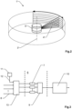
- Figure 1 schematically depicts, in a top view and in a perspective view, an embodiment of a multi-beam measurement device 1 within the scope of to the invention.
- the measurement device 1 comprises a mult-beam emitter 2, configured to generate a plurality of, e.g. pulsed, distance measuring beams.
- the plurality of measuring beams also referred to as transmission beams, are directed onto a varying deflection element, here a reflective polygon rotating around a vertical rotation axis 3.
- the plurality of transmission beams thus defines a fan 4 of distance measuring beams rotating about the rotation axis 3 (lying in a vertical plane).
- An instantaneous vertical field of view is covered by the fanned out multiple measuring beams, whereas scanning in azimuthal direction is achieved by means of the fast rotating polygon prism.
- the elevation here refers to an angle to the axis of rotation 3, typically measured from a ground plane orthogonal to the axis of rotation 3. With exactly vertical alignment of the axis of rotation 3, as shown in the figure, the elevation thus corresponds to a certain distance of height above ground.
- the measurement device 1 can be arranged in any orientation to the ground.
- the elevation in a horizontal orientation of the axis of rotation 3 corresponds to an angle to the rotation axis measured from a vertical plane.
- the multi-beam emitter 2 and the polygon prism are enclosed by a protective housing, which has window 5 allowing the transmitted and the returning radiation to pass.
- Figure 2 exemplarily shows an outer view of another multi-beam measurement device 1' within the scope of the invention, formed with a base and a rotating member (not shown) arranged rotatably on the base about a rotation axis 3' relative to the base.
- the rotating member is enclosed by a protective housing, which is fixed to the base and has a circumferential window 5' allowing the transmitted and the returning radiation to pass.
- the protective housing and a (e.g. non-circumferential) transmission and reception window could also be configured to rotate with the rotating member.
- the measurement device 1' is configured to generate a plurality of transmission beams for transmitting pulsed distance measuring radiation, wherein different elevations are scanned by different transmission beams.
- the elevation here refers to an angle to the axis of rotation 3' (similar to Fig. 1 ). With exactly vertical alignment of the axis of rotation 3', as shown in the figure, the elevation thus corresponds to a certain distance of height above ground.
- the plurality of transmission beams thus defines a fan 4' of distance measuring beams rotating about the rotation axis 3' (lying in a vertical plane).
- a circumferential field of view (field of the scanning area) may be generated, e.g. of 360 ° x 25 °, by rotating the fan 4' about the rotation axis 3'.
- a partial field of view e.g. 80 ° x 25 ° may be scanned by oscillating the fan 4' back and forth or by only generating coordinate measuring data for a particular observation window, e.g. a particular azimuthal range.
- the measurement device can also be configured to provide an extension of the vertical field of view by tilting the rotating member with respect to the rotation axis 3'.
- the transmission beams are generated by means of a plurality of laser arrays.
- Returning distance measuring beams of the different transmission beams entering a receiver objective unit are directed, e.g. in a straight or angled fashion, to a plurality of receiver arrays, e.g. based on semiconductor photomultiplier sensors (SiPM sensors or SPAD arrays) or avalanche photo diodes (APD) configured for distance measurements.
- SiPM sensors or SPAD arrays semiconductor photomultiplier sensors
- SPAD avalanche photo diodes
- the data of the measurement device 1' may then be used by a computing unit configured to derive a three-dimensional point cloud based on angle data providing the angular orientation of the rotating member about the rotation axis 3', the distance measurement data, and stored directional data providing the beam direction of each of the plurality of transmission beams.
- Figure 3 shows an exemplary embodiment of a programmable integrated circuit design, e.g. a FPGA design, to be used in a receiver circuit according to the invention.
- a programmable integrated circuit design e.g. a FPGA design
- FPGAs field-programmable gate arrays
- FPGA field-programmable gate arrays
- FPGA allow to implement a timing circuit programmed with picosecond accuracy for Lidar, which enables a compact setup of the measurement device 1 with multiple parallel measurement channels.
- no special ASIC application-specific integrated circuit
- ASIC application-specific integrated circuit
- the FPGA 6 comprises a plurality of parallel delay lines 7, wherein each delay line 7 has a plurality of delay elements (not shown), which sequentially propagate an input signal of the respective delay line, wherein each of the delay elements provides a binary output as a function of a signal change of the input signal.
- the FPGA is mounted on a printed circuit board (PCB) and receives return signals 8, each return signal corresponding to one of the emitted transmission beams.
- the outputs of each delay line 7 are provided, e.g.
- a serialization / arbitration uplink unit 9 configured to carry out a time measurement of signal changes of the return signals 8 by simultaneous consideration of the sampled binary outputs of an individual delay line 7 at a certain point in time, by further taking into account individual time delays of the delay elements of the respective delay line 7.
- the receiver circuit further comprises a reference generator 11 configured to generate a reference signal 12 having a reference signal change, wherein the reference signal is asynchronous to a sampling clock driving the sampling of the binary outputs. Furthermore, a selector 13 is used, being configured that individual ones of the delay lines 7 are fed with individual ones of the return signals 8 and that alternating each of the individual ones of the delay lines 7 is fed with the reference signal 12 instead.
- the analysis unit 10 is configured to carry out a statistical analysis of the sampled binary outputs that correspond to the reference signal 12 that propagated through one of the delay lines 7 and, based thereof, to determine individual time delays of the delay elements of the one of the delay lines and to take into account the determined individual time delays in the time measurement of the signal change when the one of the delay lines 7 is fed with one of the return signals 8.
- the TDC measures the point in time of an edge of a binary signal using a coarse and a fine measurement.
- the coarse measurement is based on counting clock cycles in the ns range (e.g. 2*10 -9 s).
- the fine measurement determines the time between clock cycles through signal propagation by asynchronous FPGA logic.
- This is achieved by chaining elementary FPGA resources such as look-up tables (LUTs), routing resources or carry logic for adders.
- LUTs look-up tables
- the use of adders currently allows the highest time resolution and is therefore beneficial for high measurement accuracy.
- the chaining of such modules is called a delay line. When the delay line is sampled one often refers to it as a tapped delay line.
- the content of the delay line is stored in one or more parallel register lines and then evaluated. The pattern in the register line, together with a calibration, allows an exact determination of the time of an edge.
- the analysis unit 10 is placed in a different FPGA (analysis FPGA) than the FPGA 6 containing the delay line. This leads to an increased performance as the switching noise, crosstalk and fluctuations of the power consumption of the analysis FPGA are located at a different position than the FPGA 6 containing the delay lines. Thus, the analysis FPGA has no influence on the individual time delays of the delay lines 7.
- Figure 4 shows an exemplary embodiment of an input channel of a receiver circuit having a comparator arrangement 14, which has several different comparators 15 driven by different switching thresholds 150, wherein each comparator 15 provides a corresponding comparator output signal 19 as a function of the corresponding switching threshold 150.
- Individual comparator output signals 19 are fed in parallel, e.g. via a selector 13 (not shown, see Fig. 3 ) to individual delay lines 7 of the plurality of parallel delay lines.
- the returning transmission pulse 16 is detected by a detector 17 and the comparator arrangement 14 receives a signal amplified by an amplifier 18.
- the comparator arrangement 14 outputs digitized signals 19 (each digitized signal 19 being associated with the returning transmission pulse 16), which are fed to several of the plurality of parallel delay lines 7 in parallel.
- FIGS. 6 and 7 schematically depict a delay channel (one delay line 7) of an FPGA useable according to the invention ( Fig. 6 ) and a corresponding timing scheme ( Fig. 7 ).
- the delay line shown by Fig. 6 comprises an input buffer 21 connected to an input channel 20 for receiving an input signal 200.
- the delay line may have 100 to 1000 delay elements 22. Each delay element causes a delay of a certain amount of time.
- the asynchronous output signal of the delay elements is sampled by registers 23 (same number of registers 23 as delay elements 22) using a highly stable sampling clock generated by an oscillator 24.
- the oscillator 24 may be followed by an FPGA-internal or external PLL for jitter reduction.
- the registers 23 are registered again at least once or twice by additional registers 25, e.g. in order to avoid metastabilities.
- a trap logic 26 determines if the data in the additional registers 25 contain an edge or not and, based thereof, the register content including values of a coarse counter 27 are provided to a FIFO 28 ("First In - First Out"). The output 29 of the FIFO 28 is then used for further processing.
- Figure 7 shows the timing scheme for the above described example, wherein the following lines are depicted: a line corresponding to the sampling clock 240, to the laser trigger 300, to the input signal 200, to the input signal propagating through the delay elements 220, to the first register 230, to the additional register 250, and to the trap logic 260, wherein at the bottom the corresponding coarse counter values 270 are indicated.
- the input signal 200 is fed through a delay line with nine delay elements 22.
- the input pulse is 1.5 clock cycles wide. This results in a binary sequence 250 of the additional registers 25 on the delay line at t 2 of 111000000, i.e. the fine point in time of the rising edge of the input pulse is at the third delay element and an edge point in time can be assigned to it (fine measurement).
- the delay elements all take the same amount of time for one pass, i.e. the rising edge is around 3/9 of a clock cycle. Normally, however, the transit times are unequal and must be calibrated.
- the falling edge can be found at time t 4 , wherein the binary sequence is 000000011, thus at around 7/9 of a clock cycle.
- the coarse counter value 270 needs to be saved as well for the final calculation at what time the edges happen.
- the width of the pulse can therefore be determined and is around 13/9, i.e. close to the original pulse width (1.5).
- the maximum measurement time of the delay line is increased. For example, this means that the coarse counter / sampling clock frequency could be lowered at the cost of lower accuracy due to jitter.
- the trap logic 26 determines from the registers 23, 25 whether a data record should be saved and processed, it must determine whether there is an edge or a pulse in the delay line. In the simplest case, it can observe the first register corresponding to the first delay element, e.g. wherein in case this changes its state, the output should be saved, otherwise not. This works for long pulses (> 1 sampling period), if shorter pulses or pulse intervals are to be detected, the trap logic 26 can be improved, wherein, for example, several registers (e.g. every 100th register of the additional registers 25) are included in the decision.
- An input pulse can also be fed into several delay lines in parallel, i.e. it can be sampled several times. This can lead to higher measurement accuracy.
- the pulse can also be directed to one delay line, which is then sampled several times by multiple parallel register lines. The additional routing delay between the delay element and register also results in higher sampling resolution, e.g. providing higher measurement accuracy.
- an inventive TDC calibration is used to determine the time delays between the neighboring delay elements in the delay line.
- this TDC calibration is carried out using a statistical measurement method (code density analysis).
- An asynchronous pulse is measured many times by the TDC and the delay of each delay element can be determined by assuming that the pulses are evenly distributed over time.
- This calibration is then used to convert the delay line information into a unit of time.
- the input can have different sources, e.g. asynchronous calibration pulses (oscillator) and measuring pulses.
- Switching input place of selector 13, see Fig. 3
- an internal or external oscillator is used for calibration.
- calibration includes alternating between reference signal and return signal, e.g. by using a selector 13 as described above.
- at least one of the delay lines is foreseen for calibration during the measurement process. Then it is switched to another delay line to be calibrated.
- each measuring channel is calibrated during the measurements, e.g. by using a calibration pulse after each measurement pulse.
- Figure 8 shows an exemplary embodiment of an emitter circuit useable in a measurement device according to the invention to precisely time the emission instant of measuring pulses.
- the above described FPGA 6 further comprises a laser pulser 35 having a trigger generator 36.
- the trigger generator 36 is configured to generate an initial laser trigger signal 38 for triggering laser pulse emission by individual laser triggers 39.
- the emitter circuit further comprises a synchronization circuit 37 configured to convert the initially noisy laser trigger signal 38 into a precise synchronized trigger signal 40 to be provided to the laser triggers 39, by synchronizing the initial trigger signal 38 with a known (jitter-free) transmission clock signal 41.
- the laser pulser 35 comprises a linking generator 42 configured to generate activation signals 43 for the transmission beams associated to the multiple laser triggers 39. Therefore, the single synchronized (high-precision) trigger signal 40 generated by the synchronizing circuit is useable to drive the individual laser triggers 39.
Landscapes
- Engineering & Computer Science (AREA)
- Physics & Mathematics (AREA)
- General Physics & Mathematics (AREA)
- Computer Networks & Wireless Communication (AREA)
- Radar, Positioning & Navigation (AREA)
- Remote Sensing (AREA)
- Electromagnetism (AREA)
- Optical Radar Systems And Details Thereof (AREA)
Claims (15)
- Dispositif de mesure (1, 1') pour capture géométrique tridimensionnelle d'un environnement avec• un émetteur multifaisceaux (2) pour émettre une pluralité de faisceaux de transmission (4),• un récepteur multifaisceaux ayant une pluralité de zones réceptrices pour recevoir des faisceaux de transmission émis de la pluralité de faisceaux de transmission de retour de l'environnement et• un circuit récepteur configuré pour générer des signaux de retour (8) qui correspondent aux faisceaux de transmission émis et à des changements de signaux de temps des signaux de retour pour dériver des temps de vol des faisceaux de transmission émis,caractérisé en ce que• le circuit récepteur comprend un circuit intégré programmable (6) qui a une pluralité de lignes à retard parallèles (7), cependant que chaque ligne à retard respective (7) de la pluralité de lignes à retard parallèles a une pluralité d'éléments retard (22) qui propagent de manière séquentielle un signal d'entrée (200) de la ligne à retard respective (7), cependant que chaque élément retard de la pluralité d'éléments retard (22) est configuré pour fournir une sortie binaire comme fonction du signal d'entrée (200),• le circuit récepteur est configuré pour exécuter une mesure du temps d'un changement de signal du signal d'entrée (200) en échantillonnant les sorties binaires de la ligne à retard respective (7) et la considération simultanée des sorties binaires échantillonnées (230, 250) à un certain point dans le temps en prenant de plus en compte des retards des éléments retard (22) et• le circuit récepteur comprend de plus∘ un générateur de référence (1) configuré pour générer un signal de référence (12) qui a un changement de signal de référence, cependant que le signal de référence est asynchrone par rapport à une horloge d'échantillonnage (24) qui entraîne l'échantillonnage des sorties binaires et∘ un sélecteur (13) configuré de telle manière que des lignes à retard individuelles sont alimentées avec des signaux de retour individuels (8) et de telle manière qu'alternativement chacune des lignes à retard individuelles (7) est alimentée à la place avec le signal de référence (12) et• le circuit récepteur est configuré pour exécuter une analyse statistique des sorties binaires échantillonnées (230, 250) qui correspondent au signal de référence (12) qui a été propagé par l'une des lignes à retard (7) et, sur la base de celle-ci, pour déterminer des retards individuels des éléments retard (22) de l'une des lignes à retard (7) et pour prendre en compte les retards individuels déterminés dans la mesure du temps du changement de signal lorsque l'une des lignes à retard (7) est alimentée avec l'un des signaux de retour (8).
- Dispositif de mesure (1, 1') selon la revendication 1,
caractérisé en ce que
les éléments retard sont configurés pour fournir les sorties binaires par reconnaissance d'un flanc montant et/ou descendant du signal d'entrée. - Dispositif de mesure (1, 1') selon la revendication 1 ou 2,
caractérisé en ce que
le circuit récepteur comprend une horloge d'échantillonnage commune (24) configurée pour entraîner de manière conjointe l'échantillonnage des sorties binaires pour toutes les lignes à retard (7). - Dispositif de mesure (1, 1') selon l'une des revendications précédentes,
caractérisé en ce quele circuit récepteur est configuré pour• compter des cycles d'horloge de l'horloge d'échantillonnage avant l'apparition du changement de signal en utilisant une logique asynchrone,• déterminer le temps écoulé entre les cycles d'horloge de l'horloge d'échantillonnage depuis l'apparition du changement de signal en utilisant une logique asynchrone,cependant que la mesure du temps du changement de signal est exécutée en combinant les cycles d'horloge comptés de l'horloge d'échantillonnage (24) et le temps écoulé entre des cycles d'horloge de l'horloge d'échantillonnage (24). - Dispositif de mesure (1, 1') selon l'une des revendications précédentes,
caractérisé en ce que,
pour chacune de la pluralité des lignes à retard parallèles (7), le circuit récepteur comprend une ligne de registre, chaque ligne de registre ayant une pluralité de registres (23, 25) associés à la pluralité d'éléments retard (22) et étant configurée pour stocker les sorties binaires. - Dispositif de mesure (1, 1') selon l'une des revendications 1 à 4,
caractérisé en ce que,• pour chacune de la pluralité des lignes à retard parallèles (7), le circuit récepteur comprend des lignes de registre multiples, chaque ligne de registre ayant une pluralité de registres (23, 25) associés à la pluralité d'éléments retard (22) et étant configurée pour stocker les sorties binaires et• le circuit récepteur est configuré de telle manière qu'un signal d'entrée (200) qui se propage par une ligne à retard respective (7) de la pluralité de lignes À retard est échantillonné individuellement par chacune des lignes de registre correspondantes. - Dispositif de mesure (1, 1') selon l'une des revendications précédentes,
caractérisé en ce que• le circuit récepteur comprend une section de distribution configurée pour générer plusieurs signaux de sortie identiques de section de distribution provenant d'un signal d'entrée de section de distribution (8, 12) et• le circuit récepteur est configuré pour alimenter des signaux de sortie de section de distribution à plusieurs de la pluralité de lignes à retard parallèles (7) en parallèle,cependant que le circuit récepteur est configuré de telle manière que la section de distribution est alimentée avec l'un des signaux de retour (8) et/ou que la section de distribution est alimentée avec le signal de référence (12). - Dispositif de mesure (1, 1') selon l'une des revendications précédentes, caractérisé en ce que• le circuit récepteur comprend des comparateurs multiples (15) fournissant différents seuils de commutation (150), chaque comparateur (15) fournissant un signal de sortie de comparateur correspondant (19) en tant que fonction du seuil de commutation correspondant (150),• le circuit récepteur est configuré de telle manière que des signaux individuels de sortie de comparateur (19) sont alimentés en parallèle à des lignes à retard individuelles (7) de la pluralité de lignes à retard parallèles et• le circuit récepteur est configuré de telle manière que les comparateurs multiples (15) sont alimentés avec des signaux d'entrée de comparateur générés à partir de l'un des signaux de retour (8) et/ou du signal de référence (12).
- Dispositif de mesure (1, 1') selon la revendication 8,
caractérisé en ce que
le circuit récepteur est configuré pour comparer les signaux de sortie de comparateur (19) pour déterminer des décalages de synchronisation dépendant de l'amplitude dans la mesure du temps du changement de signal, en particulier des décalages de synchronisation dus au déplacement en distance. - Dispositif de mesure (1, 1') selon l'une des revendications précédentes,
caractérisé en ce que
l'analyse statistique pour déterminer des décalages de synchronisation individuels des éléments retard (22) de l'une des lignes à retard (7) est basée sur des propagations multiples du signal de référence (12) par l'une des lignes à retard (7) et une supposition qu'un flanc ascendant et/ou descendant du signal de référence est réparti uniformément dans le temps. - Dispositif de mesure (1, 1') selon l'une des revendications précédentes,
caractérisé en ce que
chacune de la pluralité des lignes à retard parallèles (7) comprend au moins cent éléments retard (22). - Dispositif de mesure (1, 1') selon l'une des revendications précédentes,
caractérisé en ce quele circuit récepteur comprend une unité d'analyse (10) qui est séparée du circuit intégré programmable (6),cependant que l'unité d'analyse (10) est configurée• pour exécuter la considération simultanée des sorties binaires échantillonnées à un certain point dans le temps pour la mesure du temps du changement de signal et• pour exécuter l'analyse statistique des sorties binaires échantillonnées qui correspondent au signal de référence (12) qui s'est propagé par l'une des lignes à retard (7) et, sur la base de celle-ci, pour déterminer les retards individuels des éléments retard (22) de l'une des lignes à retard (7). - Dispositif de mesure (1, 1') selon l'une des revendications précédentes,
caractérisé en ce que
le dispositif de mesure (1, 1') comprend une électronique de pulseur laser configurée pour générer un signal de déclenchement laser synchronisé (40) pour déclencher l'émission de l'impulsion laser dans le but d'émettre la pluralité de faisceaux de transmission (4, 4'), cependant que• le circuit intégré programmable (6) comprend un générateur de déclenchement (36) configuré pour générer un signal de déclenchement initial (38) et• l'électronique de pulseur laser est configurée pour générer le signal de déclenchement laser synchronisé (40) en synchronisant le signal de déclenchement initial (38) avec un signal d'horloge de transmission connu (41), en particulier cependant que le signal d'horloge de transmission (41) est généré par la même horloge source (24) en tant qu'horloge d'échantillonnage. - Dispositif de mesure (1, 1') selon la revendication 13,
caractérisé en ce que
le dispositif de mesure (1, 1') comprend un générateur de liaison (42) et des déclencheurs laser multiples (39), cependant que• chacun des déclencheurs laser (39) est configuré pour fournir le déclenchement de l'émission d'impulsion laser dans le but d'émettre un faisceau de transmission associé de la pluralité de faisceaux de transmission (4, 4'),• les déclencheurs laser multiples (39) sont contrôlés par le même signal de déclenchement laser synchronisé (40),• le générateur de liaison (42) est configuré pour générer des signaux d'activation (43) pour les faisceaux de transmission (4, 4') associés aux déclencheurs laser multiples (39), cependant que chacun des faisceaux de transmission associés aux déclencheurs laser multiples (39) est affecté uniquement à l'un des signaux d'activation (43) et• le dispositif de mesure (1, 1') est configuré de telle manière que chacun des signaux d'activation (43) active l'émission de son faisceau de transmission associé par son déclencheur laser associé (39). - Dispositif de mesure (1, 1') selon l'une des revendications 1 à 14,
caractérisé en ce que• le circuit intégré programmable (6) comprend un générateur de déclenchement (36) configuré pour générer un signal de déclenchement laser (38),• le dispositif de mesure (1, 1') est configuré pour alimenter le signal de déclenchement laser (38) à une ligne à retard d'un autre circuit intégré programmable et, sur la base de celui-ci, pour déterminer un temps d'émission du signal de déclenchement laser (38).
Priority Applications (3)
| Application Number | Priority Date | Filing Date | Title |
|---|---|---|---|
| EP20210724.9A EP4006576B1 (fr) | 2020-11-30 | 2020-11-30 | Disposif de mesure du temps del vol multicanal avec convertisseurs temps-numérique dans un circuit intégré programmable |
| CN202111375542.3A CN114577138B (zh) | 2020-11-30 | 2021-11-19 | 用于环境的三维几何捕获的测量装置 |
| US17/537,067 US20220171038A1 (en) | 2020-11-30 | 2021-11-29 | Multichannel time-of-flight measurement device with time-to-digital converters in a programmable integrated circuit |
Applications Claiming Priority (1)
| Application Number | Priority Date | Filing Date | Title |
|---|---|---|---|
| EP20210724.9A EP4006576B1 (fr) | 2020-11-30 | 2020-11-30 | Disposif de mesure du temps del vol multicanal avec convertisseurs temps-numérique dans un circuit intégré programmable |
Publications (2)
| Publication Number | Publication Date |
|---|---|
| EP4006576A1 EP4006576A1 (fr) | 2022-06-01 |
| EP4006576B1 true EP4006576B1 (fr) | 2025-01-22 |
Family
ID=73646244
Family Applications (1)
| Application Number | Title | Priority Date | Filing Date |
|---|---|---|---|
| EP20210724.9A Active EP4006576B1 (fr) | 2020-11-30 | 2020-11-30 | Disposif de mesure du temps del vol multicanal avec convertisseurs temps-numérique dans un circuit intégré programmable |
Country Status (3)
| Country | Link |
|---|---|
| US (1) | US20220171038A1 (fr) |
| EP (1) | EP4006576B1 (fr) |
| CN (1) | CN114577138B (fr) |
Families Citing this family (3)
| Publication number | Priority date | Publication date | Assignee | Title |
|---|---|---|---|---|
| EP3657203B1 (fr) * | 2018-11-22 | 2026-04-01 | Hexagon Innovation Hub GmbH | Télémètre électrooptique et procédé de télémétrie |
| CN115113223B (zh) * | 2022-07-04 | 2026-04-21 | 杭州瑞盟科技股份有限公司 | 一种激光测距方法、装置及计算机可读存储介质 |
| CN115791574B (zh) * | 2023-02-08 | 2023-04-11 | 中国空气动力研究与发展中心低速空气动力研究所 | 一种固态与液态云粒子比例测量装置 |
Family Cites Families (5)
| Publication number | Priority date | Publication date | Assignee | Title |
|---|---|---|---|---|
| US3588349A (en) * | 1967-12-08 | 1971-06-28 | Kokusai Denshin Denwa Co Ltd | Demodulation apparatus of a phase-modulated telegraphic wave or waves |
| CN110809704B (zh) * | 2017-05-08 | 2022-11-01 | 威力登激光雷达美国有限公司 | Lidar数据获取与控制 |
| EP3455645A4 (fr) * | 2017-07-20 | 2019-04-24 | SZ DJI Technology Co., Ltd. | Systèmes et procédés de mesure de distance optique |
| CN111033312A (zh) * | 2017-08-31 | 2020-04-17 | 深圳市大疆创新科技有限公司 | 光学距离测量设备的延迟时间校准及相关联的系统和方法 |
| US10063221B1 (en) * | 2017-10-20 | 2018-08-28 | Lawrence Livermore National Security, Llc | Equivalent time sampling |
-
2020
- 2020-11-30 EP EP20210724.9A patent/EP4006576B1/fr active Active
-
2021
- 2021-11-19 CN CN202111375542.3A patent/CN114577138B/zh active Active
- 2021-11-29 US US17/537,067 patent/US20220171038A1/en active Pending
Also Published As
| Publication number | Publication date |
|---|---|
| US20220171038A1 (en) | 2022-06-02 |
| CN114577138B (zh) | 2024-06-04 |
| EP4006576A1 (fr) | 2022-06-01 |
| CN114577138A (zh) | 2022-06-03 |
Similar Documents
| Publication | Publication Date | Title |
|---|---|---|
| US11703569B2 (en) | LIDAR data acquisition and control | |
| CN111983589B (zh) | 单光子雪崩二极管(spad)微单元阵列及其操作方法 | |
| EP3834005B1 (fr) | Organe de commande d'éclairage lidar multicanaux | |
| KR102403544B1 (ko) | 방출기들의 어드레스가능 어레이를 사용하는 비행 시간 감지 | |
| EP3516415B1 (fr) | Commande de puissance de transmission adaptative pour lidar | |
| EP3593166B1 (fr) | Commande de puissance d'éclairage à lidar intégré | |
| CN107085218B (zh) | 确定返回光脉冲的返回时间的方法以及spl扫描仪 | |
| CN101449181B (zh) | 测距方法和用于确定目标的空间维度的测距仪 | |
| US20220171038A1 (en) | Multichannel time-of-flight measurement device with time-to-digital converters in a programmable integrated circuit | |
| EP4099052A1 (fr) | Convertisseur temporel-numérique en réseau | |
| US20190018119A1 (en) | Early-late pulse counting for light emitting depth sensors | |
| KR20200110451A (ko) | 고분해능 장거리 플래시 lidar를 위한 방법들 및 시스템들 | |
| EP3182156A1 (fr) | Appareil de télémétrie | |
| CN113260874A (zh) | 用于空间分布式选通的方法和系统 | |
| CN109239694A (zh) | 用于测量距离的光电传感器和方法 | |
| WO2020142948A1 (fr) | Dispositif radar laser, circuit intégré à application spécifique, et appareil de télémétrie | |
| US11971505B2 (en) | Methods and devices for peak signal detection | |
| US20250258280A1 (en) | Lidar systems for near-field and far-field detection, and related methods and apparatus | |
| KR20220106646A (ko) | 직접 tof 측정 기반 거리 센서를 위한 가변 펄스 생성기 | |
| US20220244385A1 (en) | Lidar device and method of operating the same | |
| US20230221442A1 (en) | Lidar Clocking Schemes For Power Management | |
| EP4624985A1 (fr) | Module de mesure de distance multicanal pour balayer un environnement | |
| WO2022016448A1 (fr) | Capteur tof indirect, puce de capteur empilée, et procédé de mesure de distance à un objet associé | |
| CN121899844A (zh) | 激光雷达系统以及测距方法 |
Legal Events
| Date | Code | Title | Description |
|---|---|---|---|
| PUAI | Public reference made under article 153(3) epc to a published international application that has entered the european phase |
Free format text: ORIGINAL CODE: 0009012 |
|
| STAA | Information on the status of an ep patent application or granted ep patent |
Free format text: STATUS: THE APPLICATION HAS BEEN PUBLISHED |
|
| AK | Designated contracting states |
Kind code of ref document: A1 Designated state(s): AL AT BE BG CH CY CZ DE DK EE ES FI FR GB GR HR HU IE IS IT LI LT LU LV MC MK MT NL NO PL PT RO RS SE SI SK SM TR |
|
| RIN1 | Information on inventor provided before grant (corrected) |
Inventor name: ROHNER, MARCEL Inventor name: BESTLER, SIMON Inventor name: KOLLER, ROMAN Inventor name: WOHLGENANNT, RAINER |
|
| STAA | Information on the status of an ep patent application or granted ep patent |
Free format text: STATUS: REQUEST FOR EXAMINATION WAS MADE |
|
| 17P | Request for examination filed |
Effective date: 20221130 |
|
| RBV | Designated contracting states (corrected) |
Designated state(s): AL AT BE BG CH CY CZ DE DK EE ES FI FR GB GR HR HU IE IS IT LI LT LU LV MC MK MT NL NO PL PT RO RS SE SI SK SM TR |
|
| REG | Reference to a national code |
Ref country code: DE Ref legal event code: R079 Free format text: PREVIOUS MAIN CLASS: G01S0007481000 Ipc: G01S0007487000 Ref country code: DE Ref legal event code: R079 Ref document number: 602020045088 Country of ref document: DE Free format text: PREVIOUS MAIN CLASS: G01S0007481000 Ipc: G01S0007487000 |
|
| GRAP | Despatch of communication of intention to grant a patent |
Free format text: ORIGINAL CODE: EPIDOSNIGR1 |
|
| RIC1 | Information provided on ipc code assigned before grant |
Ipc: G01S 7/481 20060101ALI20240814BHEP Ipc: G01S 7/4865 20200101ALI20240814BHEP Ipc: G01S 7/487 20060101AFI20240814BHEP |
|
| STAA | Information on the status of an ep patent application or granted ep patent |
Free format text: STATUS: GRANT OF PATENT IS INTENDED |
|
| INTG | Intention to grant announced |
Effective date: 20240919 |
|
| GRAS | Grant fee paid |
Free format text: ORIGINAL CODE: EPIDOSNIGR3 |
|
| GRAA | (expected) grant |
Free format text: ORIGINAL CODE: 0009210 |
|
| STAA | Information on the status of an ep patent application or granted ep patent |
Free format text: STATUS: THE PATENT HAS BEEN GRANTED |
|
| AK | Designated contracting states |
Kind code of ref document: B1 Designated state(s): AL AT BE BG CH CY CZ DE DK EE ES FI FR GB GR HR HU IE IS IT LI LT LU LV MC MK MT NL NO PL PT RO RS SE SI SK SM TR |
|
| REG | Reference to a national code |
Ref country code: GB Ref legal event code: FG4D |
|
| REG | Reference to a national code |
Ref country code: CH Ref legal event code: EP |
|
| REG | Reference to a national code |
Ref country code: IE Ref legal event code: FG4D |
|
| REG | Reference to a national code |
Ref country code: DE Ref legal event code: R096 Ref document number: 602020045088 Country of ref document: DE |
|
| REG | Reference to a national code |
Ref country code: NL Ref legal event code: MP Effective date: 20250122 |
|
| PG25 | Lapsed in a contracting state [announced via postgrant information from national office to epo] |
Ref country code: NL Free format text: LAPSE BECAUSE OF FAILURE TO SUBMIT A TRANSLATION OF THE DESCRIPTION OR TO PAY THE FEE WITHIN THE PRESCRIBED TIME-LIMIT Effective date: 20250122 |
|
| PG25 | Lapsed in a contracting state [announced via postgrant information from national office to epo] |
Ref country code: RS Free format text: LAPSE BECAUSE OF FAILURE TO SUBMIT A TRANSLATION OF THE DESCRIPTION OR TO PAY THE FEE WITHIN THE PRESCRIBED TIME-LIMIT Effective date: 20250422 |
|
| PG25 | Lapsed in a contracting state [announced via postgrant information from national office to epo] |
Ref country code: FI Free format text: LAPSE BECAUSE OF FAILURE TO SUBMIT A TRANSLATION OF THE DESCRIPTION OR TO PAY THE FEE WITHIN THE PRESCRIBED TIME-LIMIT Effective date: 20250122 |
|
| PG25 | Lapsed in a contracting state [announced via postgrant information from national office to epo] |
Ref country code: PL Free format text: LAPSE BECAUSE OF FAILURE TO SUBMIT A TRANSLATION OF THE DESCRIPTION OR TO PAY THE FEE WITHIN THE PRESCRIBED TIME-LIMIT Effective date: 20250122 |
|
| PG25 | Lapsed in a contracting state [announced via postgrant information from national office to epo] |
Ref country code: ES Free format text: LAPSE BECAUSE OF FAILURE TO SUBMIT A TRANSLATION OF THE DESCRIPTION OR TO PAY THE FEE WITHIN THE PRESCRIBED TIME-LIMIT Effective date: 20250122 |
|
| REG | Reference to a national code |
Ref country code: LT Ref legal event code: MG9D |
|
| PG25 | Lapsed in a contracting state [announced via postgrant information from national office to epo] |
Ref country code: NO Free format text: LAPSE BECAUSE OF FAILURE TO SUBMIT A TRANSLATION OF THE DESCRIPTION OR TO PAY THE FEE WITHIN THE PRESCRIBED TIME-LIMIT Effective date: 20250422 Ref country code: IS Free format text: LAPSE BECAUSE OF FAILURE TO SUBMIT A TRANSLATION OF THE DESCRIPTION OR TO PAY THE FEE WITHIN THE PRESCRIBED TIME-LIMIT Effective date: 20250522 |
|
| REG | Reference to a national code |
Ref country code: AT Ref legal event code: MK05 Ref document number: 1761853 Country of ref document: AT Kind code of ref document: T Effective date: 20250122 |
|
| PG25 | Lapsed in a contracting state [announced via postgrant information from national office to epo] |
Ref country code: HR Free format text: LAPSE BECAUSE OF FAILURE TO SUBMIT A TRANSLATION OF THE DESCRIPTION OR TO PAY THE FEE WITHIN THE PRESCRIBED TIME-LIMIT Effective date: 20250122 |
|
| PG25 | Lapsed in a contracting state [announced via postgrant information from national office to epo] |
Ref country code: LV Free format text: LAPSE BECAUSE OF FAILURE TO SUBMIT A TRANSLATION OF THE DESCRIPTION OR TO PAY THE FEE WITHIN THE PRESCRIBED TIME-LIMIT Effective date: 20250122 Ref country code: PT Free format text: LAPSE BECAUSE OF FAILURE TO SUBMIT A TRANSLATION OF THE DESCRIPTION OR TO PAY THE FEE WITHIN THE PRESCRIBED TIME-LIMIT Effective date: 20250522 |
|
| PG25 | Lapsed in a contracting state [announced via postgrant information from national office to epo] |
Ref country code: BG Free format text: LAPSE BECAUSE OF FAILURE TO SUBMIT A TRANSLATION OF THE DESCRIPTION OR TO PAY THE FEE WITHIN THE PRESCRIBED TIME-LIMIT Effective date: 20250122 Ref country code: GR Free format text: LAPSE BECAUSE OF FAILURE TO SUBMIT A TRANSLATION OF THE DESCRIPTION OR TO PAY THE FEE WITHIN THE PRESCRIBED TIME-LIMIT Effective date: 20250423 |
|
| PG25 | Lapsed in a contracting state [announced via postgrant information from national office to epo] |
Ref country code: AT Free format text: LAPSE BECAUSE OF FAILURE TO SUBMIT A TRANSLATION OF THE DESCRIPTION OR TO PAY THE FEE WITHIN THE PRESCRIBED TIME-LIMIT Effective date: 20250122 |
|
| PG25 | Lapsed in a contracting state [announced via postgrant information from national office to epo] |
Ref country code: SE Free format text: LAPSE BECAUSE OF FAILURE TO SUBMIT A TRANSLATION OF THE DESCRIPTION OR TO PAY THE FEE WITHIN THE PRESCRIBED TIME-LIMIT Effective date: 20250122 |
|
| PG25 | Lapsed in a contracting state [announced via postgrant information from national office to epo] |
Ref country code: SM Free format text: LAPSE BECAUSE OF FAILURE TO SUBMIT A TRANSLATION OF THE DESCRIPTION OR TO PAY THE FEE WITHIN THE PRESCRIBED TIME-LIMIT Effective date: 20250122 |
|
| PG25 | Lapsed in a contracting state [announced via postgrant information from national office to epo] |
Ref country code: DK Free format text: LAPSE BECAUSE OF FAILURE TO SUBMIT A TRANSLATION OF THE DESCRIPTION OR TO PAY THE FEE WITHIN THE PRESCRIBED TIME-LIMIT Effective date: 20250122 |
|
| PG25 | Lapsed in a contracting state [announced via postgrant information from national office to epo] |
Ref country code: IT Free format text: LAPSE BECAUSE OF FAILURE TO SUBMIT A TRANSLATION OF THE DESCRIPTION OR TO PAY THE FEE WITHIN THE PRESCRIBED TIME-LIMIT Effective date: 20250122 |
|
| PG25 | Lapsed in a contracting state [announced via postgrant information from national office to epo] |
Ref country code: CZ Free format text: LAPSE BECAUSE OF FAILURE TO SUBMIT A TRANSLATION OF THE DESCRIPTION OR TO PAY THE FEE WITHIN THE PRESCRIBED TIME-LIMIT Effective date: 20250122 Ref country code: EE Free format text: LAPSE BECAUSE OF FAILURE TO SUBMIT A TRANSLATION OF THE DESCRIPTION OR TO PAY THE FEE WITHIN THE PRESCRIBED TIME-LIMIT Effective date: 20250122 |
|
| REG | Reference to a national code |
Ref country code: DE Ref legal event code: R097 Ref document number: 602020045088 Country of ref document: DE |
|
| PG25 | Lapsed in a contracting state [announced via postgrant information from national office to epo] |
Ref country code: RO Free format text: LAPSE BECAUSE OF FAILURE TO SUBMIT A TRANSLATION OF THE DESCRIPTION OR TO PAY THE FEE WITHIN THE PRESCRIBED TIME-LIMIT Effective date: 20250122 |
|
| PG25 | Lapsed in a contracting state [announced via postgrant information from national office to epo] |
Ref country code: SK Free format text: LAPSE BECAUSE OF FAILURE TO SUBMIT A TRANSLATION OF THE DESCRIPTION OR TO PAY THE FEE WITHIN THE PRESCRIBED TIME-LIMIT Effective date: 20250122 |
|
| REG | Reference to a national code |
Ref country code: CH Ref legal event code: W10 Free format text: ST27 STATUS EVENT CODE: U-0-0-W10-W00 (AS PROVIDED BY THE NATIONAL OFFICE) Effective date: 20251119 |
|
| PLBE | No opposition filed within time limit |
Free format text: ORIGINAL CODE: 0009261 |
|
| STAA | Information on the status of an ep patent application or granted ep patent |
Free format text: STATUS: NO OPPOSITION FILED WITHIN TIME LIMIT |
|
| RAP2 | Party data changed (patent owner data changed or rights of a patent transferred) |
Owner name: HEXAGON INNOVATION HUB GMBH |
|
| 26N | No opposition filed |
Effective date: 20251023 |
|
| PGFP | Annual fee paid to national office [announced via postgrant information from national office to epo] |
Ref country code: DE Payment date: 20251119 Year of fee payment: 6 |
|
| PGFP | Annual fee paid to national office [announced via postgrant information from national office to epo] |
Ref country code: GB Payment date: 20251121 Year of fee payment: 6 |
|
| REG | Reference to a national code |
Ref country code: DE Ref legal event code: R081 Ref document number: 602020045088 Country of ref document: DE Owner name: HEXAGON INNOVATION HUB GMBH, CH Free format text: FORMER OWNER: HEXAGON TECHNOLOGY CENTER GMBH, HEERBRUGG, CH |
|
| PGFP | Annual fee paid to national office [announced via postgrant information from national office to epo] |
Ref country code: FR Payment date: 20251126 Year of fee payment: 6 |
|
| REG | Reference to a national code |
Ref country code: GB Ref legal event code: 732E Free format text: REGISTERED BETWEEN 20260305 AND 20260311 |