EP4006632A1 - Verfahren zur herstellung einer gekrümmten anzeigevorrichtung - Google Patents
Verfahren zur herstellung einer gekrümmten anzeigevorrichtung Download PDFInfo
- Publication number
- EP4006632A1 EP4006632A1 EP19940082.1A EP19940082A EP4006632A1 EP 4006632 A1 EP4006632 A1 EP 4006632A1 EP 19940082 A EP19940082 A EP 19940082A EP 4006632 A1 EP4006632 A1 EP 4006632A1
- Authority
- EP
- European Patent Office
- Prior art keywords
- display assembly
- flat display
- curved
- adhesive
- flat
- Prior art date
- Legal status (The legal status is an assumption and is not a legal conclusion. Google has not performed a legal analysis and makes no representation as to the accuracy of the status listed.)
- Granted
Links
Images






Classifications
-
- G—PHYSICS
- G02—OPTICS
- G02F—OPTICAL DEVICES OR ARRANGEMENTS FOR THE CONTROL OF LIGHT BY MODIFICATION OF THE OPTICAL PROPERTIES OF THE MEDIA OF THE ELEMENTS INVOLVED THEREIN; NON-LINEAR OPTICS; FREQUENCY-CHANGING OF LIGHT; OPTICAL LOGIC ELEMENTS; OPTICAL ANALOGUE/DIGITAL CONVERTERS
- G02F1/00—Devices or arrangements for the control of the intensity, colour, phase, polarisation or direction of light arriving from an independent light source, e.g. switching, gating or modulating; Non-linear optics
- G02F1/01—Devices or arrangements for the control of the intensity, colour, phase, polarisation or direction of light arriving from an independent light source, e.g. switching, gating or modulating; Non-linear optics for the control of the intensity, phase, polarisation or colour
- G02F1/13—Devices or arrangements for the control of the intensity, colour, phase, polarisation or direction of light arriving from an independent light source, e.g. switching, gating or modulating; Non-linear optics for the control of the intensity, phase, polarisation or colour based on liquid crystals, e.g. single liquid crystal display cells
- G02F1/133—Constructional arrangements; Operation of liquid crystal cells; Circuit arrangements
- G02F1/1333—Constructional arrangements; Manufacturing methods
- G02F1/133308—Support structures for LCD panels, e.g. frames or bezels
- G02F1/133325—Assembling processes
-
- G—PHYSICS
- G02—OPTICS
- G02F—OPTICAL DEVICES OR ARRANGEMENTS FOR THE CONTROL OF LIGHT BY MODIFICATION OF THE OPTICAL PROPERTIES OF THE MEDIA OF THE ELEMENTS INVOLVED THEREIN; NON-LINEAR OPTICS; FREQUENCY-CHANGING OF LIGHT; OPTICAL LOGIC ELEMENTS; OPTICAL ANALOGUE/DIGITAL CONVERTERS
- G02F1/00—Devices or arrangements for the control of the intensity, colour, phase, polarisation or direction of light arriving from an independent light source, e.g. switching, gating or modulating; Non-linear optics
- G02F1/01—Devices or arrangements for the control of the intensity, colour, phase, polarisation or direction of light arriving from an independent light source, e.g. switching, gating or modulating; Non-linear optics for the control of the intensity, phase, polarisation or colour
- G02F1/13—Devices or arrangements for the control of the intensity, colour, phase, polarisation or direction of light arriving from an independent light source, e.g. switching, gating or modulating; Non-linear optics for the control of the intensity, phase, polarisation or colour based on liquid crystals, e.g. single liquid crystal display cells
- G02F1/133—Constructional arrangements; Operation of liquid crystal cells; Circuit arrangements
- G02F1/1333—Constructional arrangements; Manufacturing methods
- G02F1/133308—Support structures for LCD panels, e.g. frames or bezels
- G02F1/13332—Front frames
-
- G—PHYSICS
- G02—OPTICS
- G02F—OPTICAL DEVICES OR ARRANGEMENTS FOR THE CONTROL OF LIGHT BY MODIFICATION OF THE OPTICAL PROPERTIES OF THE MEDIA OF THE ELEMENTS INVOLVED THEREIN; NON-LINEAR OPTICS; FREQUENCY-CHANGING OF LIGHT; OPTICAL LOGIC ELEMENTS; OPTICAL ANALOGUE/DIGITAL CONVERTERS
- G02F1/00—Devices or arrangements for the control of the intensity, colour, phase, polarisation or direction of light arriving from an independent light source, e.g. switching, gating or modulating; Non-linear optics
- G02F1/01—Devices or arrangements for the control of the intensity, colour, phase, polarisation or direction of light arriving from an independent light source, e.g. switching, gating or modulating; Non-linear optics for the control of the intensity, phase, polarisation or colour
- G02F1/13—Devices or arrangements for the control of the intensity, colour, phase, polarisation or direction of light arriving from an independent light source, e.g. switching, gating or modulating; Non-linear optics for the control of the intensity, phase, polarisation or colour based on liquid crystals, e.g. single liquid crystal display cells
- G02F1/133—Constructional arrangements; Operation of liquid crystal cells; Circuit arrangements
- G02F1/1333—Constructional arrangements; Manufacturing methods
-
- B—PERFORMING OPERATIONS; TRANSPORTING
- B32—LAYERED PRODUCTS
- B32B—LAYERED PRODUCTS, i.e. PRODUCTS BUILT-UP OF STRATA OF FLAT OR NON-FLAT, e.g. CELLULAR OR HONEYCOMB, FORM
- B32B17/00—Layered products essentially comprising sheet glass, or glass, slag, or like fibres
- B32B17/06—Layered products essentially comprising sheet glass, or glass, slag, or like fibres comprising glass as the main or only constituent of a layer, next to another layer of a specific material
-
- B—PERFORMING OPERATIONS; TRANSPORTING
- B32—LAYERED PRODUCTS
- B32B—LAYERED PRODUCTS, i.e. PRODUCTS BUILT-UP OF STRATA OF FLAT OR NON-FLAT, e.g. CELLULAR OR HONEYCOMB, FORM
- B32B37/00—Methods or apparatus for laminating, e.g. by curing or by ultrasonic bonding
- B32B37/12—Methods or apparatus for laminating, e.g. by curing or by ultrasonic bonding characterised by using adhesives
- B32B37/1284—Application of adhesive
- B32B37/1292—Application of adhesive selectively, e.g. in stripes, in patterns
-
- B—PERFORMING OPERATIONS; TRANSPORTING
- B32—LAYERED PRODUCTS
- B32B—LAYERED PRODUCTS, i.e. PRODUCTS BUILT-UP OF STRATA OF FLAT OR NON-FLAT, e.g. CELLULAR OR HONEYCOMB, FORM
- B32B38/00—Ancillary operations in connection with laminating processes
- B32B38/0012—Mechanical treatment, e.g. roughening, deforming, stretching
-
- B—PERFORMING OPERATIONS; TRANSPORTING
- B32—LAYERED PRODUCTS
- B32B—LAYERED PRODUCTS, i.e. PRODUCTS BUILT-UP OF STRATA OF FLAT OR NON-FLAT, e.g. CELLULAR OR HONEYCOMB, FORM
- B32B38/00—Ancillary operations in connection with laminating processes
- B32B38/18—Handling of layers or the laminate
- B32B38/1858—Handling of layers or the laminate using vacuum
-
- B—PERFORMING OPERATIONS; TRANSPORTING
- B32—LAYERED PRODUCTS
- B32B—LAYERED PRODUCTS, i.e. PRODUCTS BUILT-UP OF STRATA OF FLAT OR NON-FLAT, e.g. CELLULAR OR HONEYCOMB, FORM
- B32B7/00—Layered products characterised by the relation between layers; Layered products characterised by the relative orientation of features between layers, or by the relative values of a measurable parameter between layers, i.e. products comprising layers having different physical, chemical or physicochemical properties; Layered products characterised by the interconnection of layers
- B32B7/04—Interconnection of layers
- B32B7/12—Interconnection of layers using interposed adhesives or interposed materials with bonding properties
- B32B7/14—Interconnection of layers using interposed adhesives or interposed materials with bonding properties applied in spaced arrangements, e.g. in stripes
-
- G—PHYSICS
- G02—OPTICS
- G02F—OPTICAL DEVICES OR ARRANGEMENTS FOR THE CONTROL OF LIGHT BY MODIFICATION OF THE OPTICAL PROPERTIES OF THE MEDIA OF THE ELEMENTS INVOLVED THEREIN; NON-LINEAR OPTICS; FREQUENCY-CHANGING OF LIGHT; OPTICAL LOGIC ELEMENTS; OPTICAL ANALOGUE/DIGITAL CONVERTERS
- G02F1/00—Devices or arrangements for the control of the intensity, colour, phase, polarisation or direction of light arriving from an independent light source, e.g. switching, gating or modulating; Non-linear optics
- G02F1/01—Devices or arrangements for the control of the intensity, colour, phase, polarisation or direction of light arriving from an independent light source, e.g. switching, gating or modulating; Non-linear optics for the control of the intensity, phase, polarisation or colour
- G02F1/13—Devices or arrangements for the control of the intensity, colour, phase, polarisation or direction of light arriving from an independent light source, e.g. switching, gating or modulating; Non-linear optics for the control of the intensity, phase, polarisation or colour based on liquid crystals, e.g. single liquid crystal display cells
- G02F1/1303—Apparatus specially adapted to the manufacture of LCDs
-
- G—PHYSICS
- G02—OPTICS
- G02F—OPTICAL DEVICES OR ARRANGEMENTS FOR THE CONTROL OF LIGHT BY MODIFICATION OF THE OPTICAL PROPERTIES OF THE MEDIA OF THE ELEMENTS INVOLVED THEREIN; NON-LINEAR OPTICS; FREQUENCY-CHANGING OF LIGHT; OPTICAL LOGIC ELEMENTS; OPTICAL ANALOGUE/DIGITAL CONVERTERS
- G02F1/00—Devices or arrangements for the control of the intensity, colour, phase, polarisation or direction of light arriving from an independent light source, e.g. switching, gating or modulating; Non-linear optics
- G02F1/01—Devices or arrangements for the control of the intensity, colour, phase, polarisation or direction of light arriving from an independent light source, e.g. switching, gating or modulating; Non-linear optics for the control of the intensity, phase, polarisation or colour
- G02F1/13—Devices or arrangements for the control of the intensity, colour, phase, polarisation or direction of light arriving from an independent light source, e.g. switching, gating or modulating; Non-linear optics for the control of the intensity, phase, polarisation or colour based on liquid crystals, e.g. single liquid crystal display cells
- G02F1/133—Constructional arrangements; Operation of liquid crystal cells; Circuit arrangements
- G02F1/1333—Constructional arrangements; Manufacturing methods
- G02F1/133305—Flexible substrates, e.g. plastics, organic film
-
- G—PHYSICS
- G02—OPTICS
- G02F—OPTICAL DEVICES OR ARRANGEMENTS FOR THE CONTROL OF LIGHT BY MODIFICATION OF THE OPTICAL PROPERTIES OF THE MEDIA OF THE ELEMENTS INVOLVED THEREIN; NON-LINEAR OPTICS; FREQUENCY-CHANGING OF LIGHT; OPTICAL LOGIC ELEMENTS; OPTICAL ANALOGUE/DIGITAL CONVERTERS
- G02F1/00—Devices or arrangements for the control of the intensity, colour, phase, polarisation or direction of light arriving from an independent light source, e.g. switching, gating or modulating; Non-linear optics
- G02F1/01—Devices or arrangements for the control of the intensity, colour, phase, polarisation or direction of light arriving from an independent light source, e.g. switching, gating or modulating; Non-linear optics for the control of the intensity, phase, polarisation or colour
- G02F1/13—Devices or arrangements for the control of the intensity, colour, phase, polarisation or direction of light arriving from an independent light source, e.g. switching, gating or modulating; Non-linear optics for the control of the intensity, phase, polarisation or colour based on liquid crystals, e.g. single liquid crystal display cells
- G02F1/133—Constructional arrangements; Operation of liquid crystal cells; Circuit arrangements
- G02F1/1333—Constructional arrangements; Manufacturing methods
- G02F1/133308—Support structures for LCD panels, e.g. frames or bezels
- G02F1/133331—Cover glasses
-
- B—PERFORMING OPERATIONS; TRANSPORTING
- B32—LAYERED PRODUCTS
- B32B—LAYERED PRODUCTS, i.e. PRODUCTS BUILT-UP OF STRATA OF FLAT OR NON-FLAT, e.g. CELLULAR OR HONEYCOMB, FORM
- B32B2457/00—Electrical equipment
- B32B2457/20—Displays, e.g. liquid crystal displays, plasma displays
- B32B2457/202—LCD, i.e. liquid crystal displays
-
- B—PERFORMING OPERATIONS; TRANSPORTING
- B32—LAYERED PRODUCTS
- B32B—LAYERED PRODUCTS, i.e. PRODUCTS BUILT-UP OF STRATA OF FLAT OR NON-FLAT, e.g. CELLULAR OR HONEYCOMB, FORM
- B32B2605/00—Vehicles
- B32B2605/003—Interior finishings
-
- G—PHYSICS
- G02—OPTICS
- G02F—OPTICAL DEVICES OR ARRANGEMENTS FOR THE CONTROL OF LIGHT BY MODIFICATION OF THE OPTICAL PROPERTIES OF THE MEDIA OF THE ELEMENTS INVOLVED THEREIN; NON-LINEAR OPTICS; FREQUENCY-CHANGING OF LIGHT; OPTICAL LOGIC ELEMENTS; OPTICAL ANALOGUE/DIGITAL CONVERTERS
- G02F1/00—Devices or arrangements for the control of the intensity, colour, phase, polarisation or direction of light arriving from an independent light source, e.g. switching, gating or modulating; Non-linear optics
- G02F1/01—Devices or arrangements for the control of the intensity, colour, phase, polarisation or direction of light arriving from an independent light source, e.g. switching, gating or modulating; Non-linear optics for the control of the intensity, phase, polarisation or colour
- G02F1/13—Devices or arrangements for the control of the intensity, colour, phase, polarisation or direction of light arriving from an independent light source, e.g. switching, gating or modulating; Non-linear optics for the control of the intensity, phase, polarisation or colour based on liquid crystals, e.g. single liquid crystal display cells
- G02F1/133—Constructional arrangements; Operation of liquid crystal cells; Circuit arrangements
- G02F1/1333—Constructional arrangements; Manufacturing methods
- G02F1/133308—Support structures for LCD panels, e.g. frames or bezels
- G02F1/133314—Back frames
-
- G—PHYSICS
- G02—OPTICS
- G02F—OPTICAL DEVICES OR ARRANGEMENTS FOR THE CONTROL OF LIGHT BY MODIFICATION OF THE OPTICAL PROPERTIES OF THE MEDIA OF THE ELEMENTS INVOLVED THEREIN; NON-LINEAR OPTICS; FREQUENCY-CHANGING OF LIGHT; OPTICAL LOGIC ELEMENTS; OPTICAL ANALOGUE/DIGITAL CONVERTERS
- G02F2201/00—Constructional arrangements not provided for in groups G02F1/00 - G02F7/00
- G02F2201/56—Substrates having a particular shape, e.g. non-rectangular
-
- G—PHYSICS
- G02—OPTICS
- G02F—OPTICAL DEVICES OR ARRANGEMENTS FOR THE CONTROL OF LIGHT BY MODIFICATION OF THE OPTICAL PROPERTIES OF THE MEDIA OF THE ELEMENTS INVOLVED THEREIN; NON-LINEAR OPTICS; FREQUENCY-CHANGING OF LIGHT; OPTICAL LOGIC ELEMENTS; OPTICAL ANALOGUE/DIGITAL CONVERTERS
- G02F2202/00—Materials and properties
- G02F2202/28—Adhesive materials or arrangements
Definitions
- the present disclosure relates to a method of processing a flat display and a flat cover glass to manufacture a curved display device.
- the display device is provided with a display for displaying screen information and a cover glass for protecting the display.
- a curved cover glass In order to manufacture a curved display device, a curved cover glass must be provided therein. The curved cover glass must be processed to have the same curvature as that of the curved display.
- the curved display device has been manufactured by a method of bonding a light-transmitting adhesive layer to a flexible display and then bonding it to a curved cover glass.
- this method since curved lamination must be performed, there is a problem in that a process difficulty is increased, and a curved lamination process must be redesigned when there is a variation in a curved surface of the display device.
- an aspect of the detailed description is to provide a manufacturing method capable of easily bonding a curved display and a curved cover glass during the manufacture of the curved display.
- a method of manufacturing a curved display device including coupling a flat display, an optical clear adhesive, and a cover glass to manufacture a flat display assembly, applying an adhesive to an edge of the flat display assembly, seating the flat display assembly on a curved jig, sucking the flat display assembly to a surface of the curved jig using a vacuum hole disposed in the curved jig such that the flat display assembly is bent, and coupling a backlight unit to a region to which the adhesive is applied, wherein the coupling of a backlight unit to a region to which the adhesive is applied comprises curing the adhesive while the backlight unit is pressed to the display assembly so as to maintain a bent state of the display assembly.
- the curved jig may be provided with a plurality of vacuum holes, and the sucking of the flat display assembly to a surface of the curved jig may be performed by depressurizing an inside of the vacuum holes.
- the seating of the flat display assembly on a curved jig may be performed by a first lift pin coming into contact with a central portion of the flat display assembly and a second lift pin coming into contact with an edge portion of the flat display assembly.
- each of the first and second lift pins may include a vacuum suction pad that is vacuum-sucked to the display assembly.
- the seating of the flat display assembly on a curved jig may include seating the flat display assembly on first and second lift pins, moving the first and second lift pins to the curved jig such that the flat display assembly and the curved jig overlap each other, and descending the first and second lift pins to seat the flat display assembly on the curved jig.
- the descending of the first and second lift pins to seat the flat display assembly on the curved jig may be performed by descending the first and second lift pins until the flat display assembly comes into contact with an uppermost portion of the curved jig, and the sucking of the flat display assembly to a surface of the curved jig may be performed by descending the second lift pin.
- the sucking of the flat display assembly to a surface of the curved jig may be performed while maintaining a suction force of the vacuum suction pad provided in the second lift pin.
- the coupling of a backlight unit to a region to which the adhesive is applied may include fixing the display assembly and the backlight unit with a clamp so as to maintain the display assembly in a bent state.
- the method may further include fixing the display assembly with a clamp to maintain the display assembly in a bent state after sucking the flat display assembly to a surface of the curved jig.
- the coupling of a flat display, an optical clear adhesive, and a cover glass to manufacture a flat display assembly may be performed by roll lamination.
- a roll lamination process may be performed when a display and a cover glass are in a flat state, and thereby it is not required to design a lamination process for a curved surface.
- a curved surface of a curved jig may be changed according to a curvature of a display assembly to be implemented, thereby maximizing the productivity and profitability of a curved display.
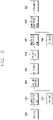
- FIG. 1 is a flowchart showing a method of bonding a curved cover glass to a display in the related art
- FIGS. 2 and 3 are conceptual views showing a method of bonding a curved cover glass to a display in the related art.
- pressing between the optical clear adhesive 110 and the flat display 130 may be performed by a roll lamination method (R), but is not limited thereto.
- removing air bubbles formed between the optical clear adhesive 110 and the flat display 130 is performed.
- the removing of the air bubbles may be carried out by atmospheric defoaming (auto clave).
- removing air bubbles formed between the optical clear adhesive 110 and the cover glass 140 (S110) is carried out.
- the removing of the air bubbles (S110) may be carried out atmospheric defoaming (auto clave).
- a state in which the cover glass 140, the optical clear adhesive 110, and the display 130 are bonded will be referred to as a display assembly 100.
- assembling a back cover to the display assembly is carried out.
- the display included in the display assembly is an LCD display
- assembling a backlight unit is carried out prior to the assembly of the back cover.
- a separate adhesive may be used to prevent separation between the back cover and the display assembly when assembling the display assembly and the back cover.
- the foregoing method in the related art has a problem in that it is difficult to implement a facility for a curved surface because roll lamination must be performed on the curved cover glass.
- the present disclosure provides a manufacturing method for implementing a curved display device using a flat cover glass and a flat display.
- the present disclosure provides a manufacturing method capable of implementing a curved display while using an existing roll lamination facility for bonding a flat cover glass and a flat display as it is.
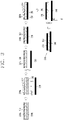
- FIGS. 3 to 6 are conceptual views showing a method of manufacturing a curved display device according to the present disclosure.
- the optical clear adhesive 210 may be a silicone-based or acrylic-based optical clear adhesive 210, but is not limited thereto.
- pressing between the optical clear adhesive 210 and the flat display 230 is performed in a roll lamination method.
- the bonding process may be performed inside a vacuum chamber.
- a pressure inside the chamber may be 10 to 1000 Pa.
- An inside of the vacuum chamber includes an adhesive chuck or an electro static chuck (ESC) capable of sucking the optical clear adhesive 210 and the display 230, and is provided with a robot or transfer device for putting and taking the display 230 therein and therefrom.
- the vacuum chamber is disposed with upper/lower adhesive chucks thereinside, and configured with suction lift pins for transferring the optical clear adhesive 210 and the display 230, and separate vacuum suction holes to fix the optical clear adhesive 210 and the display 230 to the adhesive chucks.
- a plurality of optical devices for precisely aligning the optical clear adhesive 210 and the display 230 may be disposed inside the vacuum chamber.
- depressurization inside the vacuum chamber may not be completed.
- an alignment between the optical clear adhesive 210 and the display 230 and depressurization inside the chamber are simultaneously performed.
- an alignment between the optical clear adhesive 210 and the display 230 may be performed at pressures of 100 to 1000 Pa, and a bonding process between the optical clear adhesive 210 and the display 230 may be performed in a vacuum atmosphere of 10 to 500 Pa.
- removing air bubbles formed between the optical clear adhesive 210 and the flat display 230 is carried out.
- the removing of the air bubbles may be carried out by atmospheric defoaming (auto clave).
- the defoaming condition may be performed at pressures of 3 to 15 kg/cm 2 , at temperatures of 24 to 80 °C for 4 to 15 minutes.
- An alignment between the optical clear adhesive 210 and the cover glass 240 is performed at pressures of 100 to 1000 Pa, and a bonding process between the optical clear adhesive 210 and the cover glass 240 may be performed in a vacuum atmosphere of 10 to 500 Pa.
- removing air bubbles formed between the optical clear adhesive 210 and the flat display 230 is carried out.
- the removing of the air bubbles may be carried out by atmospheric defoaming (auto clave).
- the defoaming condition may be performed at pressures of 3 to 15 kg/cm 2 , at temperatures of 24 to 80 °C for 4 to 15 minutes.
- the edge denotes an edge of the flat cover glass 240 that does not overlap the display 230.
- the adhesive 250 may be an acrylic-based, silicone-based, or urethane-based adhesive, but is not limited thereto.
- the adhesive may also be an adhesive in the form of a film.
- a curing method of the adhesive may be UV curing, thermal curing, or natural curing. The curing method of the adhesive may vary depending on the type of the adhesive.
- a first clamp C1 may be disposed at an edge of the display assembly 200.
- the first clamp C1 is not essentially required.
- a part of the backlight unit 400 is brought into contact with a position where the adhesive 250 is applied, and the adhesive 250 is cured.
- a second clamp C2 may be provided at an edge of the backlight unit 400 such that the display assembly 200 and the backlight unit 400 are strongly coupled to each other.
- the adhesive 250 is cured while the second clamp C2 is provided.
- the adhesive 250 is used for the purpose of coupling the backlight unit 400 and the back cover 500 to each other, a position to which the adhesive 250 is applied may vary depending on shapes of the backlight unit 400 and the back cover 500.
- the adhesive 250 must be applied to a region where the backlight unit 400 and the back cover 500 come into contact with each other.
- the adhesive 250 may be an acrylic-based, silicone-based, or urethane-based adhesive, but is not limited thereto.
- the adhesive 250 may be an adhesive in the form of a film.
- a curing method of the adhesive 250 may be UV curing, thermal curing, or natural curing.
- the curing method of the adhesive may vary depending on the type of the adhesive.
- the back cover 500 may be coupled to the backlight unit 400 in a state in which the adhesive layer 250 is formed in a partial region.
- the adhesive layer 250 formed on a partial region of the back cover 500 increases a coupling force between the backlight unit 400 and the back cover 500.
- a third clamp may be provided at an edge of the back cover 500 such that the back cover 500 and the backlight unit 400 are strongly coupled to each other.
- the adhesive 250 is cured in a state in which the third clamp is provided.
- a curved display is manufactured by physically bending a flat cover glass. For this reason, the present disclosure does not require a curved lamination process. Through this, the present disclosure may allow a curved display to be implemented while using an existing roll lamination facility for bonding a flat cover glass and a flat display as it is.
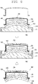
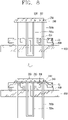
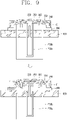
- FIGS. 7 to 11 are conceptual views showing a method of assembling a backlight unit and a back cover in a state in which a display assembly is physically bent.
- the flat display assembly 200 is put into a flat type loader unit.
- the display assembly 200 is loaded on a flat type chuck 700 by the lift pins 720.
- a plurality of holes 710 may be disposed in the flat chuck 700, and a vacuum may be formed through the holes 710 to fix the display assembly 200 to a surface of the chuck 700.
- holes are disposed in the flat chuck 700 to allow the lift pins 720 to move vertically and horizontally.
- the lift pins 720 may transfer the display assembly 200 onto the flat chuck 700 through the holes disposed in the flat chuck.
- the adhesive 250 is applied to an edge of the display assembly 200. Then, subsequent to releasing the vacuum formed in the flat chuck 700, the lift pins 720 ascend.
- the display assembly 200 is transferred to a curved jig 800.
- two types of lift pins 720a and 720b may be utilized.
- the display assembly 200 is transferred onto the curved jig 800 by the first and second lift pins 720a and 720b.
- the first lift pin 720a comes into contact with a central portion of the display assembly 200
- the second lift pin 720b comes into contact with an edge of the display assembly 200.
- each of the first and second lift pins 720a and 720b may include a vacuum suction pad that is vacuum-sucked to the display assembly 200.
- a vacuum is formed in the vacuum suction pad to fix the display assembly 200 when the first and second lift pins 720a and 720b transfer the display assembly 200.
- the curved jig 800 is a frame for processing the display assembly 200 into a curved surface.
- the first and second lift pins 720a and 720b descend.
- the first and second lift pins 720a and 720b descend until the display assembly 200 comes into contact with an uppermost portion of the curved jig 800.
- the first lift pin 720a stops descending, and a vacuum is formed through a vacuum hole 810 disposed in the curved jig 800. Accordingly, the display assembly 200 is bent.
- the second lift pin 720b descends together with the display assembly 200 according to a bending speed of the display assembly 200. At this time, the vacuum suction pad provided on the second lift pin 720b maintains a suction force, thereby providing an additional physical force to the display assembly 200. That is, in the present disclosure, the display assembly 200 is physically bent using a suction force formed by a curved jig 800 and a suction force formed by the second lift pin 720b.
- the first and second lift pins 720a and 720b descend to be completely separated from the display assembly 200.
- the clamp C1 may be mounted at an edge of the display assembly 200.
- the backlight unit 500 is coupled to a position to which the adhesive 250 is applied. Then, subsequent to mounting the clamp C2 such that the backlight unit 500 and the display assembly 200 are strongly coupled to each other, the adhesive 250 is cured.
- the display assembly 200 on which the backlight unit 500 is mounted is separated from the curved jig 800.
- the clamps mounted on the display assembly 200 and the backlight unit 500, respectively, may be sequentially separated therefrom.
- the backlight unit 500 assists in maintaining the display assembly 200 in a bent state.
- a roll lamination process may be performed when a display and a cover glass are in a flat state, and thereby it is not required to design a lamination process for a curved surface. Accordingly, as shown in FIG. 12 , a method for manufacturing a curved display device according to the present disclosure may be utilized for producing an instrument panel for a vehicle that requires display devices 1010 and 1020 having various curvatures.
- a curved surface of a curved jig may be changed according to a curvature of a display assembly to be implemented, thereby maximizing the productivity and profitability of a curved display.
Landscapes
- Physics & Mathematics (AREA)
- Nonlinear Science (AREA)
- Chemical & Material Sciences (AREA)
- Crystallography & Structural Chemistry (AREA)
- General Physics & Mathematics (AREA)
- Optics & Photonics (AREA)
- Mathematical Physics (AREA)
- Engineering & Computer Science (AREA)
- Mechanical Engineering (AREA)
- Manufacturing & Machinery (AREA)
- Devices For Indicating Variable Information By Combining Individual Elements (AREA)
- Liquid Crystal (AREA)
Applications Claiming Priority (1)
| Application Number | Priority Date | Filing Date | Title |
|---|---|---|---|
| PCT/KR2019/009446 WO2021020613A1 (ko) | 2019-07-29 | 2019-07-29 | 곡면 디스플레이 장치의 제조 방법 |
Publications (3)
| Publication Number | Publication Date |
|---|---|
| EP4006632A1 true EP4006632A1 (de) | 2022-06-01 |
| EP4006632A4 EP4006632A4 (de) | 2023-04-12 |
| EP4006632B1 EP4006632B1 (de) | 2024-11-06 |
Family
ID=74228993
Family Applications (1)
| Application Number | Title | Priority Date | Filing Date |
|---|---|---|---|
| EP19940082.1A Active EP4006632B1 (de) | 2019-07-29 | 2019-07-29 | Verfahren zur herstellung einer gekrümmten anzeigevorrichtung |
Country Status (5)
| Country | Link |
|---|---|
| US (1) | US12105368B2 (de) |
| EP (1) | EP4006632B1 (de) |
| KR (1) | KR102625687B1 (de) |
| CN (1) | CN114207513B (de) |
| WO (1) | WO2021020613A1 (de) |
Families Citing this family (1)
| Publication number | Priority date | Publication date | Assignee | Title |
|---|---|---|---|---|
| CN118700528B (zh) * | 2024-08-22 | 2025-04-08 | 深圳市磐锋精密技术有限公司 | 液晶显示屏的脱泡机及脱泡方法 |
Family Cites Families (9)
| Publication number | Priority date | Publication date | Assignee | Title |
|---|---|---|---|---|
| KR100493384B1 (ko) * | 2002-11-07 | 2005-06-07 | 엘지.필립스 엘시디 주식회사 | 액정표시소자 제조 공정용 기판 합착 장치의 기판을로딩하기 위한 구조 |
| KR20070113615A (ko) * | 2006-05-25 | 2007-11-29 | 세메스 주식회사 | 평판 디스플레이 제조용 장비 |
| JP4707697B2 (ja) | 2006-10-31 | 2011-06-22 | 日東電工株式会社 | 組み合わせ型光学フィルムの製造方法、その装置、組み合わせ型光学フィルム、画像表示装置、液晶パネルの製造方法および積層光学フィルムの製造方法 |
| US9439315B2 (en) * | 2012-06-29 | 2016-09-06 | Samsung Display Co., Ltd. | Display device, and method and apparatus for manufacturing the same |
| KR20150013987A (ko) * | 2013-07-25 | 2015-02-06 | 주식회사 유플러스비젼 | 곡면 디스플레이 패널 제조방법 및 이를 이용한 곡면 디스플레이 패널 |
| KR101746650B1 (ko) | 2014-09-02 | 2017-06-14 | 주식회사 토비스 | 곡면형 디스플레이 제조장치 및 곡면형 디스플레이 제조방법 |
| US11065960B2 (en) * | 2017-09-13 | 2021-07-20 | Corning Incorporated | Curved vehicle displays |
| KR20190053642A (ko) | 2017-11-10 | 2019-05-20 | 주식회사 에이아이코리아 | 감압을 이용한 곡면 디스플레이 접합장치 |
| KR101927801B1 (ko) | 2018-06-27 | 2019-02-26 | 주식회사 인스풀 | 곡면 디스플레이 합착 장치 및 곡면 디스플레이 합착 방법 |
-
2019
- 2019-07-29 KR KR1020217040682A patent/KR102625687B1/ko active Active
- 2019-07-29 WO PCT/KR2019/009446 patent/WO2021020613A1/ko not_active Ceased
- 2019-07-29 US US17/630,494 patent/US12105368B2/en active Active
- 2019-07-29 EP EP19940082.1A patent/EP4006632B1/de active Active
- 2019-07-29 CN CN201980099021.4A patent/CN114207513B/zh active Active
Also Published As
| Publication number | Publication date |
|---|---|
| EP4006632B1 (de) | 2024-11-06 |
| WO2021020613A1 (ko) | 2021-02-04 |
| CN114207513B (zh) | 2024-03-26 |
| EP4006632A4 (de) | 2023-04-12 |
| CN114207513A (zh) | 2022-03-18 |
| US12105368B2 (en) | 2024-10-01 |
| KR20210156293A (ko) | 2021-12-24 |
| US20220317505A1 (en) | 2022-10-06 |
| KR102625687B1 (ko) | 2024-01-17 |
Similar Documents
| Publication | Publication Date | Title |
|---|---|---|
| KR102551139B1 (ko) | 표시 장치의 제조 장치 및 그 제조 방법 | |
| US11072155B2 (en) | Laminating apparatus and method of fabricating display device using the same | |
| US10675849B2 (en) | Laminating apparatus and manufacturing method of display device | |
| JP5029523B2 (ja) | ガラス積層体、支持体付き表示装置用パネル、表示装置用パネル、表示装置およびこれらの製造方法 | |
| EP3190455B1 (de) | Anzeigevorrichtung und verfahren zur herstellung davon | |
| KR100869088B1 (ko) | 점착 척 장치 | |
| KR101765553B1 (ko) | 플렉서블 패널 곡면 합착 방법 | |
| KR102118873B1 (ko) | 플렉시블 디스플레이 및 곡면 커버 부재의 합착 장치 및 합착 방법 | |
| CN106687860B (zh) | 表皮用的支承框 | |
| KR20170106550A (ko) | 표시 장치의 제조 장치 및 제조 방법 | |
| KR20160102767A (ko) | 플렉시블 패널 곡면 합착 방법 | |
| KR20150134848A (ko) | 디스플레이패널, 패널 부착 장치 및 이를 이용한 패널 부착 방법 | |
| JP2005322815A (ja) | 半導体製造装置および半導体装置の製造方法 | |
| CN110391155B (zh) | 附着基板的方法和用于附着基板的设备 | |
| JP2018167537A (ja) | 貼合装置 | |
| EP4006632B1 (de) | Verfahren zur herstellung einer gekrümmten anzeigevorrichtung | |
| KR20210045313A (ko) | 적층 기판 및 박리 방법 | |
| JP2009186686A (ja) | カメラモジュール及びその製造方法 | |
| KR20180073987A (ko) | 커버 윈도우를 포함하는 표시 장치 및 그 제조 방법 | |
| KR101827869B1 (ko) | 박리 접합 동시 수행 장치 및 방법 | |
| KR20220064207A (ko) | 커브드 디스플레이용 합착장치 및 커브드 디스플레이를 합착하는 방법 | |
| JP2009180911A (ja) | 基板貼合せ方法、基板貼合せ装置、及びこれらの方法または装置を用いて製作したディスプレイ装置 | |
| KR20220029029A (ko) | 디스플레이 합착 장치 및 동작 방법 | |
| KR20180102734A (ko) | 윈도우 합착 장치에서 필름을 고정하는 클램프 및 이를 이용한 필름 고정 방법 | |
| US20260109142A1 (en) | Method of fabricating display device and apparatus for fabricating display device |
Legal Events
| Date | Code | Title | Description |
|---|---|---|---|
| STAA | Information on the status of an ep patent application or granted ep patent |
Free format text: STATUS: THE INTERNATIONAL PUBLICATION HAS BEEN MADE |
|
| PUAI | Public reference made under article 153(3) epc to a published international application that has entered the european phase |
Free format text: ORIGINAL CODE: 0009012 |
|
| STAA | Information on the status of an ep patent application or granted ep patent |
Free format text: STATUS: REQUEST FOR EXAMINATION WAS MADE |
|
| 17P | Request for examination filed |
Effective date: 20220223 |
|
| AK | Designated contracting states |
Kind code of ref document: A1 Designated state(s): AL AT BE BG CH CY CZ DE DK EE ES FI FR GB GR HR HU IE IS IT LI LT LU LV MC MK MT NL NO PL PT RO RS SE SI SK SM TR |
|
| DAV | Request for validation of the european patent (deleted) | ||
| DAX | Request for extension of the european patent (deleted) | ||
| A4 | Supplementary search report drawn up and despatched |
Effective date: 20230315 |
|
| RIC1 | Information provided on ipc code assigned before grant |
Ipc: G02F 1/13 20060101ALI20230309BHEP Ipc: G02F 1/1333 20060101AFI20230309BHEP |
|
| GRAP | Despatch of communication of intention to grant a patent |
Free format text: ORIGINAL CODE: EPIDOSNIGR1 |
|
| STAA | Information on the status of an ep patent application or granted ep patent |
Free format text: STATUS: GRANT OF PATENT IS INTENDED |
|
| INTG | Intention to grant announced |
Effective date: 20240729 |
|
| GRAS | Grant fee paid |
Free format text: ORIGINAL CODE: EPIDOSNIGR3 |
|
| GRAA | (expected) grant |
Free format text: ORIGINAL CODE: 0009210 |
|
| STAA | Information on the status of an ep patent application or granted ep patent |
Free format text: STATUS: THE PATENT HAS BEEN GRANTED |
|
| AK | Designated contracting states |
Kind code of ref document: B1 Designated state(s): AL AT BE BG CH CY CZ DE DK EE ES FI FR GB GR HR HU IE IS IT LI LT LU LV MC MK MT NL NO PL PT RO RS SE SI SK SM TR |
|
| REG | Reference to a national code |
Ref country code: GB Ref legal event code: FG4D |
|
| REG | Reference to a national code |
Ref country code: CH Ref legal event code: EP |
|
| REG | Reference to a national code |
Ref country code: DE Ref legal event code: R096 Ref document number: 602019061779 Country of ref document: DE |
|
| REG | Reference to a national code |
Ref country code: IE Ref legal event code: FG4D |
|
| REG | Reference to a national code |
Ref country code: LT Ref legal event code: MG9D |
|
| REG | Reference to a national code |
Ref country code: NL Ref legal event code: MP Effective date: 20241106 |
|
| PG25 | Lapsed in a contracting state [announced via postgrant information from national office to epo] |
Ref country code: PT Free format text: LAPSE BECAUSE OF FAILURE TO SUBMIT A TRANSLATION OF THE DESCRIPTION OR TO PAY THE FEE WITHIN THE PRESCRIBED TIME-LIMIT Effective date: 20250306 Ref country code: HR Free format text: LAPSE BECAUSE OF FAILURE TO SUBMIT A TRANSLATION OF THE DESCRIPTION OR TO PAY THE FEE WITHIN THE PRESCRIBED TIME-LIMIT Effective date: 20241106 Ref country code: IS Free format text: LAPSE BECAUSE OF FAILURE TO SUBMIT A TRANSLATION OF THE DESCRIPTION OR TO PAY THE FEE WITHIN THE PRESCRIBED TIME-LIMIT Effective date: 20250306 |
|
| PG25 | Lapsed in a contracting state [announced via postgrant information from national office to epo] |
Ref country code: FI Free format text: LAPSE BECAUSE OF FAILURE TO SUBMIT A TRANSLATION OF THE DESCRIPTION OR TO PAY THE FEE WITHIN THE PRESCRIBED TIME-LIMIT Effective date: 20241106 Ref country code: NL Free format text: LAPSE BECAUSE OF FAILURE TO SUBMIT A TRANSLATION OF THE DESCRIPTION OR TO PAY THE FEE WITHIN THE PRESCRIBED TIME-LIMIT Effective date: 20241106 |
|
| REG | Reference to a national code |
Ref country code: AT Ref legal event code: MK05 Ref document number: 1740009 Country of ref document: AT Kind code of ref document: T Effective date: 20241106 |
|
| PG25 | Lapsed in a contracting state [announced via postgrant information from national office to epo] |
Ref country code: BG Free format text: LAPSE BECAUSE OF FAILURE TO SUBMIT A TRANSLATION OF THE DESCRIPTION OR TO PAY THE FEE WITHIN THE PRESCRIBED TIME-LIMIT Effective date: 20241106 |
|
| PG25 | Lapsed in a contracting state [announced via postgrant information from national office to epo] |
Ref country code: ES Free format text: LAPSE BECAUSE OF FAILURE TO SUBMIT A TRANSLATION OF THE DESCRIPTION OR TO PAY THE FEE WITHIN THE PRESCRIBED TIME-LIMIT Effective date: 20241106 |
|
| PG25 | Lapsed in a contracting state [announced via postgrant information from national office to epo] |
Ref country code: NO Free format text: LAPSE BECAUSE OF FAILURE TO SUBMIT A TRANSLATION OF THE DESCRIPTION OR TO PAY THE FEE WITHIN THE PRESCRIBED TIME-LIMIT Effective date: 20250206 |
|
| PG25 | Lapsed in a contracting state [announced via postgrant information from national office to epo] |
Ref country code: GR Free format text: LAPSE BECAUSE OF FAILURE TO SUBMIT A TRANSLATION OF THE DESCRIPTION OR TO PAY THE FEE WITHIN THE PRESCRIBED TIME-LIMIT Effective date: 20250207 Ref country code: LV Free format text: LAPSE BECAUSE OF FAILURE TO SUBMIT A TRANSLATION OF THE DESCRIPTION OR TO PAY THE FEE WITHIN THE PRESCRIBED TIME-LIMIT Effective date: 20241106 Ref country code: AT Free format text: LAPSE BECAUSE OF FAILURE TO SUBMIT A TRANSLATION OF THE DESCRIPTION OR TO PAY THE FEE WITHIN THE PRESCRIBED TIME-LIMIT Effective date: 20241106 |
|
| PG25 | Lapsed in a contracting state [announced via postgrant information from national office to epo] |
Ref country code: PL Free format text: LAPSE BECAUSE OF FAILURE TO SUBMIT A TRANSLATION OF THE DESCRIPTION OR TO PAY THE FEE WITHIN THE PRESCRIBED TIME-LIMIT Effective date: 20241106 |
|
| PG25 | Lapsed in a contracting state [announced via postgrant information from national office to epo] |
Ref country code: RS Free format text: LAPSE BECAUSE OF FAILURE TO SUBMIT A TRANSLATION OF THE DESCRIPTION OR TO PAY THE FEE WITHIN THE PRESCRIBED TIME-LIMIT Effective date: 20250206 |
|
| PG25 | Lapsed in a contracting state [announced via postgrant information from national office to epo] |
Ref country code: SM Free format text: LAPSE BECAUSE OF FAILURE TO SUBMIT A TRANSLATION OF THE DESCRIPTION OR TO PAY THE FEE WITHIN THE PRESCRIBED TIME-LIMIT Effective date: 20241106 |
|
| PG25 | Lapsed in a contracting state [announced via postgrant information from national office to epo] |
Ref country code: DK Free format text: LAPSE BECAUSE OF FAILURE TO SUBMIT A TRANSLATION OF THE DESCRIPTION OR TO PAY THE FEE WITHIN THE PRESCRIBED TIME-LIMIT Effective date: 20241106 |
|
| PGFP | Annual fee paid to national office [announced via postgrant information from national office to epo] |
Ref country code: GB Payment date: 20250610 Year of fee payment: 7 |
|
| PG25 | Lapsed in a contracting state [announced via postgrant information from national office to epo] |
Ref country code: EE Free format text: LAPSE BECAUSE OF FAILURE TO SUBMIT A TRANSLATION OF THE DESCRIPTION OR TO PAY THE FEE WITHIN THE PRESCRIBED TIME-LIMIT Effective date: 20241106 |
|
| PGFP | Annual fee paid to national office [announced via postgrant information from national office to epo] |
Ref country code: FR Payment date: 20250611 Year of fee payment: 7 |
|
| PG25 | Lapsed in a contracting state [announced via postgrant information from national office to epo] |
Ref country code: RO Free format text: LAPSE BECAUSE OF FAILURE TO SUBMIT A TRANSLATION OF THE DESCRIPTION OR TO PAY THE FEE WITHIN THE PRESCRIBED TIME-LIMIT Effective date: 20241106 |
|
| PG25 | Lapsed in a contracting state [announced via postgrant information from national office to epo] |
Ref country code: SK Free format text: LAPSE BECAUSE OF FAILURE TO SUBMIT A TRANSLATION OF THE DESCRIPTION OR TO PAY THE FEE WITHIN THE PRESCRIBED TIME-LIMIT Effective date: 20241106 |
|
| PG25 | Lapsed in a contracting state [announced via postgrant information from national office to epo] |
Ref country code: CZ Free format text: LAPSE BECAUSE OF FAILURE TO SUBMIT A TRANSLATION OF THE DESCRIPTION OR TO PAY THE FEE WITHIN THE PRESCRIBED TIME-LIMIT Effective date: 20241106 |
|
| PG25 | Lapsed in a contracting state [announced via postgrant information from national office to epo] |
Ref country code: IT Free format text: LAPSE BECAUSE OF FAILURE TO SUBMIT A TRANSLATION OF THE DESCRIPTION OR TO PAY THE FEE WITHIN THE PRESCRIBED TIME-LIMIT Effective date: 20241106 |
|
| REG | Reference to a national code |
Ref country code: DE Ref legal event code: R097 Ref document number: 602019061779 Country of ref document: DE |
|
| PG25 | Lapsed in a contracting state [announced via postgrant information from national office to epo] |
Ref country code: SE Free format text: LAPSE BECAUSE OF FAILURE TO SUBMIT A TRANSLATION OF THE DESCRIPTION OR TO PAY THE FEE WITHIN THE PRESCRIBED TIME-LIMIT Effective date: 20241106 |
|
| PLBE | No opposition filed within time limit |
Free format text: ORIGINAL CODE: 0009261 |
|
| STAA | Information on the status of an ep patent application or granted ep patent |
Free format text: STATUS: NO OPPOSITION FILED WITHIN TIME LIMIT |
|
| PGFP | Annual fee paid to national office [announced via postgrant information from national office to epo] |
Ref country code: DE Payment date: 20250609 Year of fee payment: 7 |
|
| 26N | No opposition filed |
Effective date: 20250807 |
|
| REG | Reference to a national code |
Ref country code: CH Ref legal event code: H13 Free format text: ST27 STATUS EVENT CODE: U-0-0-H10-H13 (AS PROVIDED BY THE NATIONAL OFFICE) Effective date: 20260224 |
|
| PG25 | Lapsed in a contracting state [announced via postgrant information from national office to epo] |
Ref country code: LU Free format text: LAPSE BECAUSE OF NON-PAYMENT OF DUE FEES Effective date: 20250729 |
|
| REG | Reference to a national code |
Ref country code: BE Ref legal event code: MM Effective date: 20250731 |
|
| PG25 | Lapsed in a contracting state [announced via postgrant information from national office to epo] |
Ref country code: BE Free format text: LAPSE BECAUSE OF NON-PAYMENT OF DUE FEES Effective date: 20250731 |
|
| PG25 | Lapsed in a contracting state [announced via postgrant information from national office to epo] |
Ref country code: CH Free format text: LAPSE BECAUSE OF NON-PAYMENT OF DUE FEES Effective date: 20250731 |