EP4006787A1 - Dispositif à bits quantiques et procédé de fonctionnement d'un dispositif à bits quantiques - Google Patents
Dispositif à bits quantiques et procédé de fonctionnement d'un dispositif à bits quantiques Download PDFInfo
- Publication number
- EP4006787A1 EP4006787A1 EP20386054.9A EP20386054A EP4006787A1 EP 4006787 A1 EP4006787 A1 EP 4006787A1 EP 20386054 A EP20386054 A EP 20386054A EP 4006787 A1 EP4006787 A1 EP 4006787A1
- Authority
- EP
- European Patent Office
- Prior art keywords
- quantum
- qubit
- quantum well
- hole
- layer
- Prior art date
- Legal status (The legal status is an assumption and is not a legal conclusion. Google has not performed a legal analysis and makes no representation as to the accuracy of the status listed.)
- Pending
Links
Images





Classifications
-
- G—PHYSICS
- G06—COMPUTING OR CALCULATING; COUNTING
- G06N—COMPUTING ARRANGEMENTS BASED ON SPECIFIC COMPUTATIONAL MODELS
- G06N10/00—Quantum computing, i.e. information processing based on quantum-mechanical phenomena
- G06N10/40—Physical realisations or architectures of quantum processors or components for manipulating qubits, e.g. qubit coupling or qubit control
-
- G—PHYSICS
- G06—COMPUTING OR CALCULATING; COUNTING
- G06N—COMPUTING ARRANGEMENTS BASED ON SPECIFIC COMPUTATIONAL MODELS
- G06N10/00—Quantum computing, i.e. information processing based on quantum-mechanical phenomena
-
- H—ELECTRICITY
- H10—SEMICONDUCTOR DEVICES; ELECTRIC SOLID-STATE DEVICES NOT OTHERWISE PROVIDED FOR
- H10D—INORGANIC ELECTRIC SEMICONDUCTOR DEVICES
- H10D48/00—Individual devices not covered by groups H10D1/00 - H10D44/00
- H10D48/383—Quantum effect devices, e.g. of devices using quantum reflection, diffraction or interference effects
-
- H—ELECTRICITY
- H10—SEMICONDUCTOR DEVICES; ELECTRIC SOLID-STATE DEVICES NOT OTHERWISE PROVIDED FOR
- H10D—INORGANIC ELECTRIC SEMICONDUCTOR DEVICES
- H10D62/00—Semiconductor bodies, or regions thereof, of devices having potential barriers
- H10D62/10—Shapes, relative sizes or dispositions of the regions of the semiconductor bodies; Shapes of the semiconductor bodies
- H10D62/117—Shapes of semiconductor bodies
- H10D62/118—Nanostructure semiconductor bodies
-
- H—ELECTRICITY
- H10—SEMICONDUCTOR DEVICES; ELECTRIC SOLID-STATE DEVICES NOT OTHERWISE PROVIDED FOR
- H10D—INORGANIC ELECTRIC SEMICONDUCTOR DEVICES
- H10D62/00—Semiconductor bodies, or regions thereof, of devices having potential barriers
- H10D62/80—Semiconductor bodies, or regions thereof, of devices having potential barriers characterised by the materials
- H10D62/81—Semiconductor bodies, or regions thereof, of devices having potential barriers characterised by the materials of structures exhibiting quantum-confinement effects, e.g. single quantum wells; of structures having periodic or quasi-periodic potential variation
- H10D62/812—Single quantum well structures
-
- H—ELECTRICITY
- H10—SEMICONDUCTOR DEVICES; ELECTRIC SOLID-STATE DEVICES NOT OTHERWISE PROVIDED FOR
- H10D—INORGANIC ELECTRIC SEMICONDUCTOR DEVICES
- H10D64/00—Electrodes of devices having potential barriers
- H10D64/20—Electrodes characterised by their shapes, relative sizes or dispositions
- H10D64/27—Electrodes not carrying the current to be rectified, amplified, oscillated or switched, e.g. gates
-
- B—PERFORMING OPERATIONS; TRANSPORTING
- B82—NANOTECHNOLOGY
- B82Y—SPECIFIC USES OR APPLICATIONS OF NANOSTRUCTURES; MEASUREMENT OR ANALYSIS OF NANOSTRUCTURES; MANUFACTURE OR TREATMENT OF NANOSTRUCTURES
- B82Y10/00—Nanotechnology for information processing, storage or transmission, e.g. quantum computing or single electron logic
-
- H—ELECTRICITY
- H10—SEMICONDUCTOR DEVICES; ELECTRIC SOLID-STATE DEVICES NOT OTHERWISE PROVIDED FOR
- H10D—INORGANIC ELECTRIC SEMICONDUCTOR DEVICES
- H10D30/00—Field-effect transistors [FET]
- H10D30/40—FETs having zero-dimensional [0D], one-dimensional [1D] or two-dimensional [2D] charge carrier gas channels
- H10D30/47—FETs having zero-dimensional [0D], one-dimensional [1D] or two-dimensional [2D] charge carrier gas channels having two-dimensional [2D] charge carrier gas channels, e.g. nanoribbon FETs or high electron mobility transistors [HEMT]
Definitions
- the invention relates to a qubit device and to methods of operating a qubit device.
- Quantum computers have various well-known advantages over classical computers, including the ability to solve certain classes of mathematical problem with higher efficiency.
- Quantum computers use quantum bits, commonly referred to as qubits, instead of the classical bits used in a classical computer.
- a qubit device is a device used to implement a qubit.
- a promising approach for implementing a qubit is to encode information in the spin degrees of freedom of multiple electrons trapped in respective quantum dots.
- controlling such multi-electron spin encoding can be challenging, requiring complex high frequency signals and micromagnets. It has proven difficult to achieve practical scalability and high-fidelity fast readout.
- a qubit device comprising: a quantum well structure configured to host a hole gas in a quantum well; and a plurality of electrodes configured to allow the formation of a plurality of quantum dots in the hole gas and to allow encoding of a unit of quantum information in a plurality of hole spins hosted in the quantum dots.
- a qubit device is provided that is based on encoding a unit of quantum information in a plurality of hole spins rather than electron spins.
- the inventors have found that this alternative approach allows high manipulation speeds and low dephasing rates to be achieved.
- the use of holes provides strong spin orbit coupling (SOC), which leads to high manipulation speeds and, due to the low hyperfine interaction, low dephasing rates are expected.
- the hole spins are holes in Ge. Holes in Ge have particularly strong spin orbit coupling (SOC).
- SOC spin orbit coupling
- qubit devices based on hole spins can be operated at very low magnetic fields.
- the qubit devices can be operated at magnetic fields that are below the critical field for a range of superconductors, including aluminium, which allows integration with circuits that use superconducting elements, such as Josephson parametric amplifiers, superconducting resonators and superconducting quantum interference devices.
- superconducting elements such as Josephson parametric amplifiers, superconducting resonators and superconducting quantum interference devices.
- Such integration facilitates scalability and/or high-fidelity fast readout.
- the quantum well structure comprises a heterostructure of semiconductor layers. This approach allows efficient integration with existing semiconductor manufacturing technologies.
- the quantum information is encoded into singlet and triplet states of the hole spins hosted in the plurality of quantum dots, for example in a double quantum dot (DQD).
- DQD double quantum dot
- the inventors have demonstrated particularly efficient operation in this regime, with a Ge hole spin qubit in a DQD device being shown to be operable at very low fields, including below the critical field of aluminium.
- the quantum well structure comprises a quantum well layer comprising more than 90% Ge, preferably isotopically purified Ge.
- the use of isotopically purified Ge reduces a magnetic noise contribution (due to reduced amounts of Ge isotopes having nuclear spin), allowing additional improvements in qubit coherence and quality.
- the device implements X-rotations on the Bloch sphere of the qubit using the g-factor difference between hole spins and an applied magnetic field, wherein the applied magnetic field is preferably below 100mT (optionally significantly lower, such as below 1 0mT).
- the applied magnetic field is preferably below 100mT (optionally significantly lower, such as below 1 0mT).
- a qubit device comprises a quantum well structure 2 and a plurality of electrodes 15, as exemplified in Figures 1 and 2 .
- the quantum well structure 2 is configured to host a hole gas.
- the hole gas is a two-dimensional hole gas.
- the hole gas could alternatively be a one-dimensional hole gas.
- the electrodes 15 are configured to allow the formation of a plurality of quantum dots in the hole gas.
- the electrodes 15 are further configured to allow encoding of a unit of quantum information in a plurality of hole spins in the quantum dots.
- the unit of quantum information is encoded into singlet and triplet states of the hole spins hosted in the quantum dots.
- the plurality of quantum dots in which the unit of quantum information is encoded may consist of a double quantum dot (i.e. two quantum dots).
- the quantum well structure 2 may comprise a quantum well formed within a heterostructure of semiconductor layers.
- the heterostructure of semiconductor layers may be provided on a substrate W, such as a silicon wafer.
- the quantum well structure 2 comprises a quantum well layer 12 sandwiched between two confinement layers.
- the quantum well layer 12 may comprise a semiconductor with a relatively small bandgap (commonly referred to as a quantum well) and the confinement layers may comprise semiconductors with larger bandgaps.
- the two confinement layers comprise a lower confinement layer 11 and an upper confinement layer 13.
- the quantum well layer 12 may comprise more than 90% Ge, preferably more than 95% Ge, preferably more than 96% Ge, preferably more than 97% Ge, preferably more than 98% Ge, preferably more than 99% Ge.
- the Ge in the quantum well layer 12 comprises, consists essentially of, or consists of isotopically purified Ge (with reduced amounts of Ge isotope having nuclear spin relative to naturally occurring Ge).
- the Ge in the quantum well layer 12 may comprise, consist essentially of, or consist of, naturally occurring Ge.
- the thickness of the quantum well layer 12 may be in the range of 1-50nm, preferably 5-25nm, preferably 10-20nm.
- Either or both of the confinement layers 11 and 13 may comprise, consist essentially of, or consist of, SiGe with a Si content in the range of 5-50% and a Ge content in the range of 95-50%.
- the Si content is in the range of 5-40%, even more preferably in the range of 20-40%.
- the quantum well structure 2 may comprise an oxide support layer 14 for supporting the electrodes 15, as exemplified in Figure 1 .
- Either or both of the confinement layers 11 and 13 may have a thickness in the range of 10-200nm, preferably 10-100nm, preferably 20-60nm.
- the quantum well structure 2 may be formed using Ge on insulator technology.
- either or both of the confinement layers may comprise an oxide layer.
- the lower confinement layer 11 may comprise SiO 2 and the upper confinement layer 13 may comprise any oxide suitable for supporting the electrodes 15.
- the upper confinement layer 13 of the embodiment of Figure 2 might be the same oxide layer as oxide support layer 14 of the embodiment of Figure 1 .
- the upper confinement layer 13 of Figure 2 and/or the oxide support layer 14 of Figure 1 preferably has a thickness in the range of 5-50nm, preferably 5-35nm.
- the upper confinement layer 13 of Figure 2 and/or the oxide support layer 14 of Figure 1 may comprise, consist essentially of, or consist of, one or more of the following, optionally formed by atomic layer deposition: aluminium oxide, hafnium oxide, zirconium oxide (or any other high dielectric constant oxide).
- the layer may be grown for example at a temperature between 50-300C using atomic layer deposition.
- the electrodes 15 may comprise a plurality of gates.
- the electrodes 15 may be metallic.
- the gates may be configured to operate in a depletion mode, in which case they may be referred to as depletion gates.
- the gates may be configured to operate in an accumulation mode, in which case they may be referred to as accumulation gates.
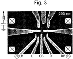
- An example arrangement for the electrodes 15 (gates) is described below with reference to Figure 3 .
- a first quantum dot is formed between gates LB and CB and a second quantum dot is formed between gates CB and RB.
- the lower gates (LB, L, CB, R, RB) thus form a double quantum dot (DQD) system.
- the upper gates tune a charge sensor (CS) dot.
- CS charge sensor
- the separation gates in the middle are tuned to maximize the CS sensitivity to charge transitions in the DQD.
- An LC-circuit connected to a CS ohmic contact allows fast read-out through microwave reflectometry.
- LB and RB are further connected to fast gate lines enabling fast control of the energy levels in the DQD.
- a quantum well is used to form the qubit by using gate electrodes to create quantum dots in the quantum well. Holes are localized in these quantum dots. The spin of the localized holes is used to encode the quantum information of the qubit. To operate the qubit, it is necessary to send appropriate electrical signals to the gate electrodes and to use a magnetic field.
- the qubit can be read out (i.e. the unit of quantum information encoded in the hole spins of the double quantum dot can be read out, in the example shown) in various ways.
- the qubit is read out via charge sensing using a nearby quantum dot (the upper three terminals in Figure 3 ).
- a quantum point contact could be used for the charge sensing.
- the qubit can be read out by dispersive read out (reflectometry with lumped elements or using a superconducting resonator).
- the read out may use the Paulispin blockade (PSB) phenomenon, which effectively provides a type of spin to charge conversion that allows the spin state of the qubit to be probed.
- PPB Paulispin blockade
- the qubit may be operated by performing rotations about two axes on the Bloch sphere of the qubit. This allows access to any point on the Bloch sphere, which is useful for quantum computation.
- X and Z rotations are implemented. The X and Z rotations allow access to the full Bloch sphere.
- the device is configured to implement X-rotations on the Bloch sphere of the qubit using a g-factor difference between the hole spins in the quantum dots (e.g. in a double quantum dot) upon application of a small magnetic field.
- the qubit is initialized in one state (e.g. a singlet state) and an electrical pulse is applied using the electrodes. The consequence of this electrical pulse is that the state is not any more an eigenstate (if the hole g-factors in the quantum dots are different). As a consequence, oscillations occur, which if the exchange interaction is sufficiently low can be about the X axis (or an axis near to the X-axis.
- the X-rotations correspond to oscillations between the singlet and triplet T 0 states.
- the magnetic field may be below 100mT, preferably below 50mT, preferably below 25mT, preferably below 10mT (as achieved in the examples discussed below).
- the device may thus be configured to apply electrical signals to the electrodes 15 and to apply a magnetic field to the quantum well structure 2.
- the device may thus comprise any suitable electrical equipment for providing these functionalities (e.g. power sources, circuit equipment, magnets, etc.).
- the magnetic field is provided using a superconducting magnet or a permanent magnet.
- the magnetic field can be created with a ferromagnetic insulator (such as EuS) or a micromagnet made out ofNi, Co or Fe for example.
- the magnetic field can point at any orientation.
- the X-rotation frequency can be electrically tuned by making use of the tunability of hole g-factors.
- Z-rotations on the Bloch sphere can be implemented by making use of the exchange interaction, i.e. wavefunction overlap between the quantum dots. Z-rotations may thus be switched on by allowing wavefunction overlap between the quantum dots.
- the qubit may be initialized in one state (e.g. a singlet state).
- the electrodes may then be used to apply an electrical pulse that brings the qubit system close to the equator of the Bloch sphere and, subsequently, the electrodes may be used to increase the exchange interaction (by increasing wavefunction overlap, for example by lowering the tunnel barrier potential) to cause rotation about the Z axis (or about an axis near to the Z axis).
- Qubits according to the present disclosure could be integrated with Ge gatemon qubits (based on Ge Josephson junctions) implemented in the same heterostructure as well as with superconducting resonators fabricated out of Al, Nb or granular Al and Josephson parametric amplifiers.
- the qubit will typically be operated at very low temperatures.
- the qubit was measured at around 20mK. It may be possible to measure the qubit at higher temperatures, for example in the range of 10mK to 4K.
- the qubit device uses Ge hole spins in a double quantum dot (DQD).
- DQD double quantum dot
- the quantum well structure 2 was provided as a strained SiGe ⁇ Ge ⁇ SiGe heterostructure grown by low-energy plasma-enhanced chemical vapor deposition (LEP- ECVD). Holes confined in a quantum well of this example are of heavy-hole (HH) type because compressive strain and confinement move light-holes (LHs) to higher energies.
- HH heavy-hole
- LHs light-holes
- the related Kramers doublet of the spin S z ⁇ 3/2 states therefore resembles an effective spin-1/2 system,
- FIG 3 is a scanning electron microscope (SEM) image of a gate layout used for implementing the control arrangement of this example.
- Single layer devices can be fabricated because without the application of any negative accumulation voltage a charge carrier density of 9.7 ⁇ 10 11 cm -2 was measured.
- Secondary Ion Mass Spectrometry (SIMS) analysis rules out boron doping in the region of the QW as a source of this carrier density. Without wishing to be bound by theory, it is believed that the high carrier density arises due to the p-type background doping of the Si wafer on which the quantum well structure was formed or due to the existing dislocations and vacancies, in combination with fixed negative charges in the deposited gate oxide.
- the two tunnel coupled quantum dots are formed by depletion gates as depicted in Figure 3 .
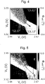
- the device can be tuned in the single hole transport regime, as shown by the stability diagrams in Figures 4 and 5 , where the sensor dot reflected phase signal ( ⁇ refl ) is displayed as a function of the voltage on L and R gates shown in Figure 3 .
- Each Coulomb blocked region corresponds to a fixed hole occupancy, and is labelled by ( N L , N R ) , with N L ( N R ) being the number of holes in the left (right) quantum dot.
- Interdot and dot-lead charge transitions appear as steep changes in the sensor signal. It is possible to deplete the left quantum dot completely while still observing charge transitions at the highest possible voltage on R. Therefore, a precise determination of the hole number in the right dot is not possible.
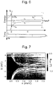
- FIG. 6 A DQD spectrum for a finite B field is shown in Figure 6 (upper graph).
- the triplet states T(2,0) lie high up in energy and are not shown.
- the two molecular singlets are split at resonance by the tunnel coupling 2 ⁇ 2 t C .
- the triplets are almost unaffected.
- ⁇ ⁇ ⁇ and the unpolarized triplet T 0 1 2
- the S - T 0 coupling can be controlled both directly via the magnetic field and by electric fields affecting the g-factors.
- the dashed trajectory 31 corresponds to a perfect X-rotation while the effective rotation axis is tilted by an angle ⁇ from the Z-axis due to a finite residual J (indicated by an arrow pointing along the Z-axis).
- X-rotations are controlled by ⁇ g and magnetic field and the resulting rotation axis is indicated by arrow 32.
- the real trajectory and rotation axis are indicated respectively by labels 61 and 62.
- the system is first initialized in (2,0) in a singlet, then pulsed quickly deep into (1,1) where the holes are separated.
- the state evolves in a plane tilted by ⁇ as depicted in Figure 8 .
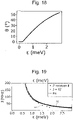
- Variation of the angle ⁇ as a function of magnetic field B, given by ⁇ arctan J 2.8 meV ⁇ g ⁇ B B , is shown in Figure 11 .
- ⁇ S After a separation time ⁇ S the system is brought quickly to the measurement point in (2,0) where PSB enables the distinction of triplet and singlet.
- the average of each column has been subtracted to account for variations in the reflectometry signal caused by magnetic field.
- a low (high) signal corresponds to a higher singlet (triplet) probability.
- Each point is integrated for 100 ms under continuous pulsing.
- the variation of the frequency f as a function of magnetic field B is depicted in Figure 12 .
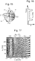
- State evolution on the Bloch sphere is depicted in Figure 15 .
- the pulse sequence used to perform Z-rotations is depicted in Figure 16 .
- J f ⁇ 2 ⁇ ⁇ g ⁇ B B h 2 and can be obtained by extracting the oscillation frequency from Figure 17 .
- the extracted values of J are plotted in Figure 19 with the darker markers 36 obtained from the exchange oscillation frequency.
- T 2 * depends on electric noise on J and magnetic noise affecting ⁇ E Z : 1
- T 2 * ⁇ 2 h J ⁇ E tot dJ d ⁇ ⁇ ⁇ rms 2 + ⁇ E Z E tot ⁇ ⁇ E Z rms 2
- ⁇ rms is the rms noise on detuning
- ⁇ ⁇ E Z rms is the magnetic noise. It is assumed that d ⁇ E Z d ⁇ ⁇ 0 as almost no change in ⁇ g with detuning is observed.
- V CB affects both t C and ⁇ g
- V LB and V RB affect mostly T C and leave ⁇ g unaltered.
- This exceptional tunability enables electrical engineering of the potential landscape to favor fast operations without negatively affecting the coherence times, thus enhancing the quality factor of this qubit.
- T 2 * reported here is already comparable to electron singlet-triplet qubits in natural Si, a reduction in the magnetic noise contribution by isotopic purification will further improve qubit coherence and quality.
- Figure 24 depicts state evolution on the Bloch sphere.
- the state evolves on the trajectory 50.
- the exchange pulse may be referred to as a refocusing pulse.
- the state again evolves on the trajectory 50 after the trajectory 51.
- the refocusing pulse is then calibrated to apply a ⁇ -pulse that brings the state on the same trajectory (i.e. the trajectory 50) as before the refocusing pulse.
- t ⁇ x is the time needed for a ⁇ -rotation along the trajectory 50.
- the free evolution time after the last refocusing pulse ⁇ S' is varied in length from ⁇ S - ⁇ t to ⁇ S + ⁇ t as depicted in Figures 25 and 26 (for one and two refocussing pulses respectively).
- Figure 27 depicts the normalized echo amplitude as a function of total separation time for the resulting oscillations. Solid lines are a fit to A E exp ⁇ t / T 2 Echo with A E being the normalized echo amplitude.
- the inventors have thus shown coherent 2-axis control of a hole singlet-triplet qubit in Ge with dephasing times of 1 ⁇ s at 0.5 mT.
- X-oscillations were driven by magnetic field differences generated either by nuclear spins or by fabricated micromagnets.
- the inventors have taken advantage of an intrinsic property of heavy hole states in Ge, namely their large and electrically tunable g-factors. They have shown electrically driven X-rotation frequencies approaching 150 MHz at fields of 5mT, which are larger than most of the reported hole spin qubit Rabi frequencies.
- Latched or shelved read-out could circumvent the decay of T 0 to S during read-out opening the exploration of the qubit's behavior at slightly higher magnetic fields where the X-rotation frequencies could surpass the highest electron-dipole spin-resonance (EDSR) Rabi frequencies reported so far, without suffering from reduced dephasing times. Furthermore, by moving towards symmetric operation or resonant driving the quality of exchange oscillations can be increased since the qubit is operated at an optimal working point. The long coherence times combined with fast and simple operations at extremely low magnetic fields make this qubit an optimal candidate for integration into a large scale quantum processor.
- EDSR electron-dipole spin-resonance
- the samples were processed in the IST Austria Nanofabrication Facility.
- a 6 ⁇ 6 mm 2 chip was cut out from a 4 inch wafer and cleaned before further processing.
- the Ohmic contacts were first patterned in a 100 keV electron beam lithography system, then a few nm of native oxide and the SiGe spacer were milled down by argon bombardment and subsequently a layer of 60 nm Pt was deposited in situ under an angle of 5°, to obtain reproducible contacts. No additional intentional annealing was performed.
- a mesa of 90 nm was etched in a reactive ion etching step.
- the native SiO 2 was removed by a 10s dip in buffered HF before the gate oxide was deposited.
- the oxide is a 20 nm ALD grown aluminium oxide (Al 2 O 3 ) grown at 300°C, which unintentionally anneals the Ohmic contacts resulting in a low resistance contact to the carriers in the quantum well.
- the top gates were first patterned via e-beam lithography and then a Ti/Pd 3/27 nm layer was deposited in an electron beam evaporator. The thinnest gates are 30 nm wide and 30 nm apart. An additional thick gate metal layer was subsequently written and deposited and served to overcome the Mesa step and allow wire bonding of the sample without shorting gates together. Quantum dots were formed by means of depletion gates (as shown in Figure 3 ).
- the lower gates form a double quantum dot (DQD) system and the upper gates tune a charge sensor (CS) dot.
- the separation gates in the middle are tuned to maximize the CS sensitivity to charge transitions in the DQD.
- An LC-circuit connected to a CS ohmic contact allows fast read-out through microwave reflectometry.
- LB and RB are further connected to fast gate lines enabling fast control of the energy levels in the DQD.
Landscapes
- Engineering & Computer Science (AREA)
- General Physics & Mathematics (AREA)
- Theoretical Computer Science (AREA)
- Physics & Mathematics (AREA)
- Mathematical Analysis (AREA)
- Data Mining & Analysis (AREA)
- Evolutionary Computation (AREA)
- Condensed Matter Physics & Semiconductors (AREA)
- Computational Mathematics (AREA)
- Mathematical Optimization (AREA)
- Pure & Applied Mathematics (AREA)
- Computing Systems (AREA)
- General Engineering & Computer Science (AREA)
- Mathematical Physics (AREA)
- Software Systems (AREA)
- Artificial Intelligence (AREA)
- Superconductor Devices And Manufacturing Methods Thereof (AREA)
Priority Applications (4)
| Application Number | Priority Date | Filing Date | Title |
|---|---|---|---|
| EP20386054.9A EP4006787A1 (fr) | 2020-11-25 | 2020-11-25 | Dispositif à bits quantiques et procédé de fonctionnement d'un dispositif à bits quantiques |
| EP21785860.4A EP4252157A1 (fr) | 2020-11-25 | 2021-09-28 | Dispositif à bits quantiques et procédé de fonctionnement d'un dispositif à bits quantiques |
| PCT/EP2021/076627 WO2022111885A1 (fr) | 2020-11-25 | 2021-09-28 | Dispositif à bits quantiques et procédé de fonctionnement d'un dispositif à bits quantiques |
| US18/038,244 US20240119333A1 (en) | 2020-11-25 | 2021-09-28 | Qubit device and method of operating a qubit device |
Applications Claiming Priority (1)
| Application Number | Priority Date | Filing Date | Title |
|---|---|---|---|
| EP20386054.9A EP4006787A1 (fr) | 2020-11-25 | 2020-11-25 | Dispositif à bits quantiques et procédé de fonctionnement d'un dispositif à bits quantiques |
Publications (1)
| Publication Number | Publication Date |
|---|---|
| EP4006787A1 true EP4006787A1 (fr) | 2022-06-01 |
Family
ID=73855494
Family Applications (2)
| Application Number | Title | Priority Date | Filing Date |
|---|---|---|---|
| EP20386054.9A Pending EP4006787A1 (fr) | 2020-11-25 | 2020-11-25 | Dispositif à bits quantiques et procédé de fonctionnement d'un dispositif à bits quantiques |
| EP21785860.4A Withdrawn EP4252157A1 (fr) | 2020-11-25 | 2021-09-28 | Dispositif à bits quantiques et procédé de fonctionnement d'un dispositif à bits quantiques |
Family Applications After (1)
| Application Number | Title | Priority Date | Filing Date |
|---|---|---|---|
| EP21785860.4A Withdrawn EP4252157A1 (fr) | 2020-11-25 | 2021-09-28 | Dispositif à bits quantiques et procédé de fonctionnement d'un dispositif à bits quantiques |
Country Status (3)
| Country | Link |
|---|---|
| US (1) | US20240119333A1 (fr) |
| EP (2) | EP4006787A1 (fr) |
| WO (1) | WO2022111885A1 (fr) |
Family Cites Families (4)
| Publication number | Priority date | Publication date | Assignee | Title |
|---|---|---|---|---|
| TW201312558A (zh) * | 2011-09-02 | 2013-03-16 | Nat Univ Tsing Hua | 石墨烯單三谷態量子位元器及其方法 |
| US9082637B2 (en) * | 2012-08-17 | 2015-07-14 | The University Of Connecticut | Optoelectronic integrated circuit |
| US11114530B2 (en) * | 2017-12-17 | 2021-09-07 | Intel Corporation | Quantum well stacks for quantum dot devices |
| US11748649B2 (en) * | 2019-12-13 | 2023-09-05 | Intel Corporation | Apparatus and method for specifying quantum operation parallelism for a quantum control processor |
-
2020
- 2020-11-25 EP EP20386054.9A patent/EP4006787A1/fr active Pending
-
2021
- 2021-09-28 EP EP21785860.4A patent/EP4252157A1/fr not_active Withdrawn
- 2021-09-28 US US18/038,244 patent/US20240119333A1/en active Pending
- 2021-09-28 WO PCT/EP2021/076627 patent/WO2022111885A1/fr not_active Ceased
Non-Patent Citations (3)
| Title |
|---|
| ANDREA HOFMANN ET AL: "Assessing the potential of Ge/SiGe quantum dots as hosts for singlet-triplet qubits", ARXIV.ORG, CORNELL UNIVERSITY LIBRARY, 201 OLIN LIBRARY CORNELL UNIVERSITY ITHACA, NY 14853, 13 October 2019 (2019-10-13), XP081514836 * |
| HENDRICKX N W ET AL: "A four-qubit germanium quantum processor", ARXIV.ORG, CORNELL UNIVERSITY LIBRARY, 201 OLIN LIBRARY CORNELL UNIVERSITY ITHACA, NY 14853, 9 September 2020 (2020-09-09), XP081758937 * |
| SAMMAK A ET AL: "Low disordered, stable, and shallow germanium quantum wells: a playground for spin and hybrid quantum technology", ARXIV.ORG, CORNELL UNIVERSITY LIBRARY, 201 OLIN LIBRARY CORNELL UNIVERSITY ITHACA, NY 14853, 7 September 2018 (2018-09-07), XP081267802, DOI: 10.1002/ADFM.201807613 * |
Also Published As
| Publication number | Publication date |
|---|---|
| US20240119333A1 (en) | 2024-04-11 |
| WO2022111885A1 (fr) | 2022-06-02 |
| EP4252157A1 (fr) | 2023-10-04 |
Similar Documents
| Publication | Publication Date | Title |
|---|---|---|
| Jirovec et al. | A singlet-triplet hole spin qubit in planar Ge | |
| AU2014234949B2 (en) | Quantum computing with acceptor-based qubits | |
| US10482388B1 (en) | Spin-orbit qubit using quantum dots | |
| Vrijen et al. | Electron-spin-resonance transistors for quantum computing in silicon-germanium heterostructures | |
| Kiršanskas et al. | Yu-Shiba-Rusinov states in phase-biased superconductor–quantum dot–superconductor junctions | |
| Petrović et al. | Colloquium: Quantum properties and functionalities of magnetic skyrmions | |
| KR20010030601A (ko) | 양자 컴퓨터 | |
| De Palma et al. | Strong hole-photon coupling in planar ge: probing the charge degree and wigner molecule states | |
| Dsouza et al. | Heavy hole vs. light hole spin qubits: a strain-driven study of SiGe/Ge and GeSn/Ge | |
| Loss et al. | Electron spins in quantum dots as quantum bits | |
| EP4006787A1 (fr) | Dispositif à bits quantiques et procédé de fonctionnement d'un dispositif à bits quantiques | |
| Jirovec et al. | A sub-millitesla Ge spin qubit | |
| Zarassi | From quantum transport in semiconducting nanowires to hybrid semiconducting-superconducting qubits | |
| Ansaloni et al. | Single-electron control in one-and two-dimensional arrays of silicon quantum dots | |
| Bertrand | Long-range transfer of spin information using individual electrons | |
| 박재민 | Implementing electron spin qubits in silicon quantum dot | |
| Heidtfeld | Investigation of spin current generated THz transients in materials with high spin-orbit coupling | |
| Scherübl | Spin-orbit interaction and superconductivity in InAs nanowire-based quantum dots devices | |
| Ragunathan | Nuclear Spin Phenomena in III-V and II-VI Semiconductor Quantum Dots | |
| Landolt | Spin-and angle-resolved photoelectron spectroscopy on topological insulators and bulk Rashba systems | |
| Bedell | Sweet-spot operation of a germanium hole spin qubit with highly anisotropic noise sensitivity | |
| Luyken et al. | Charging dynamics in vertically aligned InAs quantum dots | |
| Deng | Quantum Transport in Topological Magnets | |
| NIEGEMANN | Lecture haute fidélité des spins d'électrons dans les boîtes quantiques silicium mos high fidelity readout of electron spins in silicon mos quantum dots | |
| Andersen | Topological and Edge Transport in Two-Dimensional Electron Systems |
Legal Events
| Date | Code | Title | Description |
|---|---|---|---|
| PUAI | Public reference made under article 153(3) epc to a published international application that has entered the european phase |
Free format text: ORIGINAL CODE: 0009012 |
|
| STAA | Information on the status of an ep patent application or granted ep patent |
Free format text: STATUS: THE APPLICATION HAS BEEN PUBLISHED |
|
| AK | Designated contracting states |
Kind code of ref document: A1 Designated state(s): AL AT BE BG CH CY CZ DE DK EE ES FI FR GB GR HR HU IE IS IT LI LT LU LV MC MK MT NL NO PL PT RO RS SE SI SK SM TR |