EP4006881A1 - Anzeigetafel und anzeigevorrichtung - Google Patents
Anzeigetafel und anzeigevorrichtung Download PDFInfo
- Publication number
- EP4006881A1 EP4006881A1 EP19932267.8A EP19932267A EP4006881A1 EP 4006881 A1 EP4006881 A1 EP 4006881A1 EP 19932267 A EP19932267 A EP 19932267A EP 4006881 A1 EP4006881 A1 EP 4006881A1
- Authority
- EP
- European Patent Office
- Prior art keywords
- component
- bending
- via hole
- display panel
- layer
- Prior art date
- Legal status (The legal status is an assumption and is not a legal conclusion. Google has not performed a legal analysis and makes no representation as to the accuracy of the status listed.)
- Pending
Links
Images



Classifications
-
- H—ELECTRICITY
- H10—SEMICONDUCTOR DEVICES; ELECTRIC SOLID-STATE DEVICES NOT OTHERWISE PROVIDED FOR
- H10K—ORGANIC ELECTRIC SOLID-STATE DEVICES
- H10K77/00—Constructional details of devices covered by this subclass and not covered by groups H10K10/80, H10K30/80, H10K50/80 or H10K59/80
- H10K77/10—Substrates, e.g. flexible substrates
- H10K77/111—Flexible substrates
-
- G—PHYSICS
- G09—EDUCATION; CRYPTOGRAPHY; DISPLAY; ADVERTISING; SEALS
- G09F—DISPLAYING; ADVERTISING; SIGNS; LABELS OR NAME-PLATES; SEALS
- G09F9/00—Indicating arrangements for variable information in which the information is built-up on a support by selection or combination of individual elements
- G09F9/30—Indicating arrangements for variable information in which the information is built-up on a support by selection or combination of individual elements in which the desired character or characters are formed by combining individual elements
-
- H—ELECTRICITY
- H10—SEMICONDUCTOR DEVICES; ELECTRIC SOLID-STATE DEVICES NOT OTHERWISE PROVIDED FOR
- H10K—ORGANIC ELECTRIC SOLID-STATE DEVICES
- H10K50/00—Organic light-emitting devices
- H10K50/80—Constructional details
- H10K50/868—Arrangements for polarized light emission
-
- H—ELECTRICITY
- H10—SEMICONDUCTOR DEVICES; ELECTRIC SOLID-STATE DEVICES NOT OTHERWISE PROVIDED FOR
- H10K—ORGANIC ELECTRIC SOLID-STATE DEVICES
- H10K50/00—Organic light-emitting devices
- H10K50/80—Constructional details
- H10K50/87—Arrangements for heating or cooling
-
- H—ELECTRICITY
- H10—SEMICONDUCTOR DEVICES; ELECTRIC SOLID-STATE DEVICES NOT OTHERWISE PROVIDED FOR
- H10K—ORGANIC ELECTRIC SOLID-STATE DEVICES
- H10K59/00—Integrated devices, or assemblies of multiple devices, comprising at least one organic light-emitting element covered by group H10K50/00
- H10K59/10—OLED displays
- H10K59/12—Active-matrix OLED [AMOLED] displays
- H10K59/122—Pixel-defining structures or layers, e.g. banks
-
- H—ELECTRICITY
- H10—SEMICONDUCTOR DEVICES; ELECTRIC SOLID-STATE DEVICES NOT OTHERWISE PROVIDED FOR
- H10K—ORGANIC ELECTRIC SOLID-STATE DEVICES
- H10K59/00—Integrated devices, or assemblies of multiple devices, comprising at least one organic light-emitting element covered by group H10K50/00
- H10K59/10—OLED displays
- H10K59/12—Active-matrix OLED [AMOLED] displays
- H10K59/131—Interconnections, e.g. wiring lines or terminals
-
- H—ELECTRICITY
- H10—SEMICONDUCTOR DEVICES; ELECTRIC SOLID-STATE DEVICES NOT OTHERWISE PROVIDED FOR
- H10K—ORGANIC ELECTRIC SOLID-STATE DEVICES
- H10K59/00—Integrated devices, or assemblies of multiple devices, comprising at least one organic light-emitting element covered by group H10K50/00
- H10K59/40—OLEDs integrated with touch screens
-
- H—ELECTRICITY
- H10—SEMICONDUCTOR DEVICES; ELECTRIC SOLID-STATE DEVICES NOT OTHERWISE PROVIDED FOR
- H10K—ORGANIC ELECTRIC SOLID-STATE DEVICES
- H10K59/00—Integrated devices, or assemblies of multiple devices, comprising at least one organic light-emitting element covered by group H10K50/00
- H10K59/80—Constructional details
- H10K59/8793—Arrangements for polarized light emission
-
- H—ELECTRICITY
- H10—SEMICONDUCTOR DEVICES; ELECTRIC SOLID-STATE DEVICES NOT OTHERWISE PROVIDED FOR
- H10K—ORGANIC ELECTRIC SOLID-STATE DEVICES
- H10K59/00—Integrated devices, or assemblies of multiple devices, comprising at least one organic light-emitting element covered by group H10K50/00
- H10K59/80—Constructional details
- H10K59/8794—Arrangements for heating and cooling
-
- H—ELECTRICITY
- H10—SEMICONDUCTOR DEVICES; ELECTRIC SOLID-STATE DEVICES NOT OTHERWISE PROVIDED FOR
- H10K—ORGANIC ELECTRIC SOLID-STATE DEVICES
- H10K2102/00—Constructional details relating to the organic devices covered by this subclass
- H10K2102/301—Details of OLEDs
- H10K2102/311—Flexible OLED
-
- Y—GENERAL TAGGING OF NEW TECHNOLOGICAL DEVELOPMENTS; GENERAL TAGGING OF CROSS-SECTIONAL TECHNOLOGIES SPANNING OVER SEVERAL SECTIONS OF THE IPC; TECHNICAL SUBJECTS COVERED BY FORMER USPC CROSS-REFERENCE ART COLLECTIONS [XRACs] AND DIGESTS
- Y02—TECHNOLOGIES OR APPLICATIONS FOR MITIGATION OR ADAPTATION AGAINST CLIMATE CHANGE
- Y02E—REDUCTION OF GREENHOUSE GAS [GHG] EMISSIONS, RELATED TO ENERGY GENERATION, TRANSMISSION OR DISTRIBUTION
- Y02E10/00—Energy generation through renewable energy sources
- Y02E10/50—Photovoltaic [PV] energy
- Y02E10/549—Organic PV cells
Definitions
- the present disclosure relates to the field of display technologies, and in particular, to a display panel and a display device.
- Flexible display panels are gaining more and more attention because of their advantages of light weight, thinness, bendability, foldability, and good mechanical properties.
- the flexible display panel is usually fabricated on a flexible carrier.
- the area where the control chip is bound onto the flexible display panel is bent to the back of the display area to achieve a narrow bezel design.
- the present disclosure provides a display panel and a display device, and the technical solutions are as follows:
- a display panel including:
- the bending component includes a first bending subcomponent connected to the first component and a second bending subcomponent connected to the second component; and the via hole includes a first hole in the first bending subcomponent and a second hole in the second bending subcomponent, and an orthographic projection of the first hole onto a plane of the display surface and an orthographic projection of the second hole onto the plane of the display surface at least partially coincide.
- the orthographic projection of the first hole onto the plane of the display surface completely coincides with the orthographic projection of the second hole onto the plane of the display surface.
- the first hole communicates with the second hole.
- a number of the via hole is 1, and the via hole passes through the bending component in a thickness direction of the bending component.
- the bending component has a plurality of via holes arranged in an array in a direction parallel to a bending axis, and each of the via holes passes through the bending component in a thickness direction of the bending component.
- the via hole extends into the first component and the second component.
- the first component has a fan-out area, an edge area, and a display area sequentially arranged in a direction away from the bending component, and the via hole extends to the fan-out area.
- the bending component has opposing first and second sides, the first side joins the first component, and the second side joins the second component;
- the via hole is located at the center of the bending component in a first direction parallel to a bending axis of the bending component.
- a size of the via hole in the first direction ranges from 7 to 9 mm
- a size of the via hole in a second direction ranges from 3 to 4 mm, the second direction being perpendicular to the first direction.
- the bending component has a bending portion symmetrically arranged on both sides of the via hole in the first direction, and the bending portion is provided with signal lines extending to the second component and connected to signal leads in the fan-out area of the first component.
- the signal lines in the bending portion includes a first power signal line, a first data signal line, a second power signal line and a second data signal line that are arranged insulatedly and sequentially in a direction away from the via hole.
- the display panel further includes a control chip, wherein the signal lines in the second component are connected to the control chip through a chip-on-film film.
- the display area of the first component includes a flexible base substrate, and an active layer, a first insulation layer, a first gate electrode layer, a second insulation layer, a second gate electrode layer, an interlayer dielectric layer, a first source-drain electrode layer, a passivation layer, a first planarizing layer, a second source-drain electrode layer, a second planarizing layer, a metal conductive layer, a pixel-defining layer, a light-emitting device and a packaging layer sequentially arranged in a direction away from the flexible base substrate.
- a region of the first component on a side of the via hole distal from the second component includes the flexible base substrate, and the interlayer dielectric layer, the first source-drain electrode layer, the passivation layer, and the packaging layer sequentially arranged in a direction away from the flexible base substrate;
- a number of the via hole is 1, and the via hole passes through the bending component in a thickness direction of the bending component;
- a display device including the display panel of any one of the above aspect.
- the display device further includes: a support structure, a cover plate located on a side of the first component distal from the second component, and a bottom plate located on a side of the second component distal from the first component; wherein a first end of the support structure is connected to the cover plate, a second end of the support structure is connected to the bottom plate, and an orthographic projection of the support structure onto the cover plate and an orthographic projection of the via hole onto the cover plate has an overlapping area.
- the orthographic projection of the support structure onto the cover plate is within the orthographic projection of the via hole onto the cover plate.
- a preparation material of the support structure includes one of plastic and metal materials.
- the preparation material of the cover plate includes one of an organic resin material and an inorganic flexible material.
- the display device further includes a touch layer and a polarizer located on a side of the first component distal from the second component and stacked in a direction away from the first component.
- the display device further includes a heat dissipation film on a side of the first component proximal to the second component.
- the display device further includes g a support assembly between the heat dissipation film and the second component, a first end of the support assembly is connected to the heat dissipation film, and a second end of the support assembly is connected to the second component.
- a display device including:
- a surface of the first component distal from the second component is a display surface
- the support structure includes a plurality of columnar structures arranged in an array in a first direction parallel to a bending axis of the bending component.
- the surface of the first component distal from the second component is the display surface
- the support structure is a row structure extending in a first direction parallel to the bending axis of the bending component.
- a length of the support structure in the first direction is equal to a length of the bending component in the first direction.
- the display panel includes the display panel of any one of claims 1 to 18.
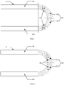
- FIG. 1 is a schematic structural diagram of a display panel provided by an embodiment of the present disclosure. As shown in FIG. 1 , the display panel includes: a first component 101, a second component 102, and a bending component 103 connecting the first component 101 and the second component 102.
- the first component 101 has a display surface A
- the bending component 103 has a via hole H passing through the bending component 103 in the direction substantially perpendicular to the display surface A.
- a direction being substantially perpendicular to the display surface means that the angle between the direction and the perpendicular direction of the display surface is less than an angle threshold.
- the direction substantially perpendicular to the display surface refers to a direction with an angle less than 5° from the perpendicular direction of the display surface.
- the first component is a display component (i.e., a display screen), and the second component is a bonding component.
- the side of the first component distal from the second component is the display surface of the display panel.
- the above display surface refers to the display surface of the foldable screen when it is completely deployed.
- the bonding component has an area for bonding a control chip, and this area may be referred to as a bonding area of the display panel.
- the via hole(s) passing through the bending component when the bending component is in a bent state, the via hole(s) is/are beneficial for releasing the internal stress of the bending component, so as to achieve a balance in stress of the respective areas of the bending component, thereby ensuring the structural stability and reliability of the display panel.
- the via hole in the bending components may be used to accommodate a support structure.
- the glass cover plate used in the conventional display device with a flexible cover plate.
- the flexible cover plate will be easily deformed when subjected to external forces such as a press, and will in turn exert a force on the film layer underneath the flexible cover plate and influence the structural stability of the film layer.
- the signal lines may break when subjected to an external force, which results in a risk.
- the via hole in the bending component passes through the bending component in a direction substantially perpendicular to the display surface, by accommodating the support structure in the via hole, one end of the support structure accommodated in the via hole may be connected with the flexible cover plate when the display panel is encapsulated with the flexible cover plate.
- the support structure can provide a great supporting effect to avoid the breakage of the signal lines in the bending component due to the external force thereon, thereby ensuring the mechanical performance of the display panel.
- the bending component 103 may include a first bending subcomponent 1031 connected to the first component 101 and a second bending subcomponent 1032 connected to the second component 102.
- the via hole H includes a first hole H1 in the first bending subcomponent 1031 and a second hole H2 in the second bending subcomponent 1032, that is, the via hole H is composed of the first hole H1 and the second hole H2.
- the orthographic projection of the first hole H1 onto the plane of the display surface A and the orthographic projection of the second hole H2 onto the plane of the display surface A at least partially coincide.
- the bending component is divided into the first bending subcomponent and the second bending subcomponent. This is only for the purpose of explaining the positions of the via holes conveniently, and the first bending subcomponent and the second bending subcomponent are actually still an integrated structure.
- the orthographic projection of the first hole onto the plane of the display surface completely coincides with the orthographic projection of the second hole onto the plane of the display surface.
- the first hole and the second hole have the same aperture size, and a support structure that matches the aperture size of the first and second holes can be selected.
- the support structure passes through the first hole and the second hole, the first hole and the second hole may effectively limit the position of the support structure in a direction parallel to the display surface.
- FIG. 2 is a schematic structural diagram of another display panel provided by an embodiment of the present disclosure. As shown in FIG. 2 , the first hole H1 in the first bending subcomponent 1031 and the second hole H2 in the second bending subcomponent 1032 communicate with each other.
- the number of the via hole(s) in the bending component may be 1, and the via hole passes through the bending component in the thickness direction of the bending component.
- the bending component may have a plurality of via holes arranged in an array in a direction parallel to the bending axis, and each via hole passes through the bending component in the thickness direction of the bending component.
- the structure of the display panel will be further described by taking the number of via holes in the bending component being 1 as an example in the embodiment of the present disclosure.
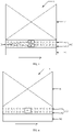
- FIG. 3 is a schematic diagram of the display panel shown in FIG. 1 being deployed
- FIG. 4 is a schematic diagram of the display panel shown in FIG. 2 being deployed.
- the via hole H is located at the center of the bending component 103 in the first direction x which is parallel to the bending axis of the bending component 103.
- the via hole H is a rectangular via hole, as an example.
- the via hole may also be a circular via hole, an irregular-shaped via hole, or via hole with other shape.
- the embodiment of the present disclosure does not limit the shape of the via hole.
- the support structure can have a uniform protection effect on the structure of the bending component on both sides of the via hole in the first direction, thereby ensuring the mechanical performance of the display panel.
- a via hole is formed in the bending component, and then the bending component is bent to obtain a display panel.
- the display panel shown in FIG. 3 is formed first, and then the display panel shown in FIG. 3 is bent to obtain a final display panel.
- the via hole in the bending component passes through the bending component in the thickness direction of the bending component.
- a via hole can be formed in the bending component to obtain a display panel.
- the via hole in the bending component passes through the bending component in a direction perpendicular to the display surface of the first component. For example, reference can be made to FIGS. 1 and 2 .
- FIG. 5 is a schematic structural diagram of yet another display panel provided by an embodiment of the present disclosure
- FIG. 5 is a schematic structural diagram of the display panel in which the bending structure is in a flatly deployed state.
- the first component 101 has a fan-out area A1, an edge area A2 and a display area A3 sequentially arranged in a direction away from the bending component 103, and the via hole H extends to the fan-out area A1.
- the via hole extends to the fan-out area, when forming the signal leads in the fan-out area, it is necessary to circumvent the position of the via hole to prevent the open fault of the signal leads in the fan-out area when forming the hole.
- the bending component 103 has opposing first and second sides, the first side joins the first component 101, and the second side joins the second component 102.
- the maximum distance L1 from the edge of the via hole H in the first component 101 to the first side ranges from 145 to 155 microns; the maximum distance L2 from the edge of the via hole H in the second component 102 to the second side ranges from 1.2 to 1.6 mm.
- the size M1 of the via hole H in the first direction x ranges from 7 to 9 mm
- the size M2 of the via hole H in the second direction y ranges from 3 to 4 mm
- the second direction y is perpendicular to the first direction x.
- the bending component 103 has a bending portion W located symmetrically on both sides of the via hole H in the first direction x.
- signal lines extending to the second component 102 are provided in the bending portion W.
- the signal lines are connected to the signal leads in the fan-out area A1 of the first component 101.
- the signal lines in the bending portion W include a first power signal line D1, a first data signal line K1, a second power signal line D2, and a second data signal line K2 that are arranged insulatedly and sequentially in a direction away from the via hole H.
- the first power signal line may be a VSS signal line
- the second power signal line may be a VDD signal line.
- the minimum distance L3 between the via hole H and the first power signal line D1 ranges from 0.8 to 1.2 mm.
- the display panel further includes a control chip (not shown in the figure), and the signal lines in the second component 102 are connected to the control chip through a chip-on-film film (not shown in the figure).
- a driving chip may be integrated in the control chip, and the first data signal line and the second data signal line in the bending portion are used to connect the data line in the first component and the driving chip in the second component.
- the fan-out area A1 of the first component 101 is used to lead out various signal lines in the display area A3 and collect them to the bending portion W of the bending component 103; the signal lines in the bending portion W have a strong bending ability, and are used to connect the various signal lines in the display area A3 to the second component 102.
- FIG. 6 is a schematic cross-sectional diagram of the display panel shown in FIG. 5 at the aa' position.
- the display area of the first component includes a flexible base substrate 201, and an active layer 202, a first insulation layer 203, a first gate electrode layer 204, a second insulation layer 205, a second gate electrode layer 206, an interlayer dielectric layer 207, a first source-drain electrode layer 208, a passivation layer 209, a first planarizing layer 210, a second source-drain electrode layer 211, a second planarizing layer 212, a metal conductive layer 213, a pixel-defining layer 214, a light-emitting device 215 and a packaging layer 216 sequentially arranged in a direction away from the flexible base substrate 201.
- the metal conductive layer 213 may be an anode layer
- the light-emitting device may include a hole injection layer, a hole transport layer, a light-emitting material layer, an electron transport layer, an electron injection layer, and a cathode layer sequentially disposed in a direction away from the flexible base substrate.
- the light-emitting device may be an organic light-emitting diode (OLED) device.
- FIG. 7 is a schematic cross-sectional diagram of the display panel shown in FIG. 5 at the bb' position.
- the region of the first component 101 on the side of the via hole H distal from the second component 102 includes the flexible base substrate 201, and the interlayer dielectric layer 207, the first source-drain electrode layer 208, the passivation layer 209 and the packaging layer 216 sequentially disposed in a direction away from the flexible base substrate 201.
- the region of the second component 102 on the side of the via hole H distal from the first component 101 includes the flexible base substrate 201, and the interlayer dielectric layer 207, the passivation layer 209, the first planarizing layer 210, the second planarizing layer 212, and the pixel-defining layer 214 sequentially disposed in a direction away from the flexible base substrate 201.
- the film layers in the region adjacent to the via hole in the second component are all non-conductive film layers, that is, the signal lines in the second component are arranged to circumvent the via hole.
- FIG. 8 is a schematic cross-sectional diagram of the display panel shown in FIG. 5 at the cc' position.
- the region, where the first power signal line is located, in the bending portion of the bending component includes the flexible base substrate 201, and a flexible material layer 217, the first source-drain electrode layer 208, the first planarizing layer 210, the second source-drain electrode layer 211, the second planarizing layer 212, and the pixel-defining layer 214 sequentially arranged in a direction away from the flexible base substrate 201.
- the first power signal line, the first data signal line, the second power signal line, and the second data signal line in the bending portion are all in a two-layer structure including the first source-drain electrode layer and the second source-drain electrode layer; signal lines in the fan-out area connected to the first power signal line and the second power signal line are formed by stacking the first source-drain electrode layer and the second source-drain electrode layer. The signal lines in the fan-out area connected to the first data signal line and the second data signal line are formed by stacking the first gate electrode layer and the second gate electrode layer.
- a flexible material layer may be provided as an entire layer in the bending portion of the bending component to enhance the toughness of the bending component.
- the flexible material layer may be formed of polyimide (PI) or polyethylene terephthalate (PET) material.
- the via hole(s) passing through the bending component, when the bending component is in a bent state, the via hole(s) is/are beneficial for releasing the internal stress of the bending component, so as to achieve a balance in stress of the respective areas of the bending component, thereby ensuring the structural stability and reliability of the display panel.
- the via hole in the bending component passes through the bending component in a direction substantially perpendicular to the display surface, by accommodating the support structure in the via hole, one end of the support structure accommodated in the via hole may be connected with the flexible cover plate when the display panel is encapsulated with the flexible cover plate.
- the support structure can provide a great supporting effect to avoid the breakage of the signal lines in the bending component due to the external force thereon, thereby ensuring the mechanical performance of the display panel.
- An embodiment of the present disclosure provides a display device including the display panel as shown in any one of FIGS. 1 to 8 .
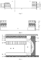
- FIG. 9 is a schematic structural diagram of a display device provided by an embodiment of the present disclosure.
- the display device includes a display panel as shown in FIG. 2 , a support structure 30, a cover plate 40 on the side of the first component 101 distal from the second component 102, and a bottom plate 50 on the side of the second component 102 distal from the first component 101.
- the bottom plate may also be referred to as a back plate, and may be a casing of the display device.
- the first end of the support structure 30 is connected to the cover plate 40, and the second end of the support structure 30 is connected to the bottom plate 50.
- the orthographic projection of the support structure 30 onto the cover plate 40 and the orthographic projection of the via hole H onto the cover plate 40 have overlapping areas. That is, at least partial structure of the support structure is within the via hole of the bending component.
- FIG. 10 is a schematic structural diagram of another display device provided by an embodiment of the present disclosure.
- the display device includes the display panel shown in FIG. 1
- the orthographic projection of the support structure 30 onto the cover plate 40 is within the orthographic projection of the via hole H onto the cover plate 40.
- the first component is a display component
- the second component is a bonding component
- the display device further includes a control chip (not shown in the figure) connected to the second component.
- the support structure is made of a rigid material.
- the preparation material of the support structure may include one of plastic and metal materials.
- the cover plate is made of a flexible material, that is, the cover plate may be a flexible cover plate, so as to realize the bendable and/or foldable function of the display device.
- the preparation material of the cover plate may include one of an organic resin material and an inorganic flexible material.
- the organic resin material may be a PI material or PET material
- the inorganic flexible material may be an ultra-thin glass.
- the display device may further include a touch layer 60 and a polarizer 70 which are located on the side of the first component 101 distal from the second component 102 and are stacked in a direction away from the first component 101.
- the display device further includes a heat dissipation film 80 on the side of the first component 101 proximal to the second component 102.
- the heat dissipation film is used for heat dissipation, to avoid the overheat temperature of the display component that may influence the normal operation of internal devices.
- the display device may further include a support assembly 90 between the heat dissipation film 80 and the second component 102, the first end of the support assembly 90 is connected to the heat dissipation film 80, and the second end of the support assembly 90 is connected to the second component 102.
- the support assembly is used for supporting and limiting position. As the second component is connected to the first component through the bending component, there is a gap between the second component and the first component.
- a supporting effect can be provided to the first component and the heat dissipation film, the touch layer and the polarizer on the both sides of the first component, on the other hand, the relative position of the first component and the second component can be defined, so as to ensure the structural stability of the display device.
- the via hole passing through the bending component in a direction perpendicular to the display surface is provided in the bending component of the display panel, by providing a support structure in the via hole, the first end of the support structure is connected to the cover plate and the second end of the support structure is connected to the bottom plate.
- the support structure can provide a great supporting effect to avoid the breakage of the signal lines in the bending component due to the external force thereon, thereby ensuring the mechanical performance of the display device.
- the support structure is within the via hole in the bending component, there is no need to increase the width of the edge of the display device, which facilitates the realization of the narrow bezel design of the display device.
- FIG. 11 is a schematic structural diagram of a display device provided by another embodiment of the present disclosure. As shown in FIG. 11 , the display device includes: a display panel, a support structure 30, a cover plate 40 and a bottom plate 50.
- the display panel includes a first component 101, a second component 102, and a bending component 103 connecting the first component 101 and the second component.
- the cover plate 40 is located on the side of the first component 101 distal from the second component 102.
- the bottom plate 50 is located on the side of the second component 102 distal from the first component 101.
- the support structure 30 is located on the side of the bending component 103 distal from the first component 101 and the second component 102. The first end of the support structure 30 is connected to the cover plate 40, and the second end of the support structure 30 is connected to the bottom plate 50.
- the first component is a display component
- the second component is a bonding component.
- the display device further includes a control chip (not shown in the figure) connected to the second component.
- the display panel may also be a display panel as shown in any one of FIGS. 1 to 8 .
- the first end of the support structure is connected to the cover plate and the second end of the support structure is connected to the bottom plate.
- the support structure can provide a great supporting effect to avoid the breakage of the signal lines in the bending component due to the external force thereon, thereby ensuring the mechanical performance of the display device.
- FIG. 12 is a schematic diagram showing a cross-section of the support structure in the display device shown in FIG. 11 at the dd' position.
- the support structure 30 may include a plurality of columnar structures 301 arranged in an array along a first direction x which is parallel to the bending axis of the bending component.
- the first direction is the direction perpendicular to the paper plane.
- FIG. 13 is schematic diagram showing another cross-section of the support structure in the display device shown in FIG. 11 at the dd' position.
- the support structure 30 is a row structure extending in the first direction x which is parallel to the bending axis of the bending component.
- the length of the support structure 30 in the first direction x in FIGS. 12 and 13 is equal to the length of the bending component in the first direction.
- the support structure can provide a supporting effect and protect the bending component from external forces, thereby preventing the signal lines in the bending component from breaking.
- the cover plate is made of a flexible material, that is, the cover plate may be a flexible cover plate, so as to achieve the bendable and/or foldable function for the display device.
- the preparation material of the cover plate may include one of an organic resin material and an inorganic flexible material.
- the organic resin material may be a PI material or PET material, and the inorganic flexible material may be ultra-thin glass.
- the display device may further include a touch layer 60 and a polarizer 70 that are located on a side of the first component 101 distal from the second component 102 and are stacked in a direction away from the first component 101.
- the display device may further include a heat dissipation film 80 on the side of the first component 101 proximal to the second component 102.
- the heat dissipation film is used for heat dissipation, so as to avoid the overheat temperature of the display component that may influence the normal operation of internal devices.
- the display device may further include a support assembly 90 between the heat dissipation film 80 and the second component 102.
- the first end of the support assembly 90 is connected to the heat dissipation film 80, and the second end of the support assembly 90 is connected to the second component 102.
- the support assembly is used for supporting and limiting position. As the second component is connected to the first component through the bending component, there is a gap between the second component and the first component.
- a supporting effect can be provided to the first component and the heat dissipation film, the touch layer and the polarizer on the both sides of the first component, on the other hand, the relative position of the first component and the second component can be defined, so as to ensure the structural stability of the display device.
- the first end of the support structure is connected to the cover plate and the second end of the support structure is connected to the bottom plate.
- the support structure can provide a great supporting effect to avoid the breakage of the signal lines in the bending component due to the external force thereon, thereby ensuring the mechanical performance of the display device.
- first and second are only used for descriptive purposes and should not be construed as indicating or implying relative importance.
- the term “a plurality of” refers to two or more, unless explicitly defined otherwise.
Landscapes
- Engineering & Computer Science (AREA)
- Physics & Mathematics (AREA)
- Microelectronics & Electronic Packaging (AREA)
- Optics & Photonics (AREA)
- Devices For Indicating Variable Information By Combining Individual Elements (AREA)
- General Physics & Mathematics (AREA)
- Theoretical Computer Science (AREA)
- Electroluminescent Light Sources (AREA)
Applications Claiming Priority (1)
| Application Number | Priority Date | Filing Date | Title |
|---|---|---|---|
| PCT/CN2019/098533 WO2021016912A1 (zh) | 2019-07-31 | 2019-07-31 | 显示面板及显示装置 |
Publications (2)
| Publication Number | Publication Date |
|---|---|
| EP4006881A1 true EP4006881A1 (de) | 2022-06-01 |
| EP4006881A4 EP4006881A4 (de) | 2022-07-27 |
Family
ID=74229634
Family Applications (1)
| Application Number | Title | Priority Date | Filing Date |
|---|---|---|---|
| EP19932267.8A Pending EP4006881A4 (de) | 2019-07-31 | 2019-07-31 | Anzeigetafel und anzeigevorrichtung |
Country Status (4)
| Country | Link |
|---|---|
| US (2) | US11785812B2 (de) |
| EP (1) | EP4006881A4 (de) |
| CN (1) | CN112639930A (de) |
| WO (1) | WO2021016912A1 (de) |
Families Citing this family (10)
| Publication number | Priority date | Publication date | Assignee | Title |
|---|---|---|---|---|
| WO2021016912A1 (zh) * | 2019-07-31 | 2021-02-04 | 京东方科技集团股份有限公司 | 显示面板及显示装置 |
| US12439799B2 (en) * | 2021-12-09 | 2025-10-07 | Samsung Display Co., Ltd. | Display apparatus and method of manufacturing the same |
| US12464635B2 (en) * | 2022-04-24 | 2025-11-04 | Chengdu Boe Optoelectronics Technology Co., Ltd. | Flexible printed circuit board and method for manufacturing the same, and display device |
| CN114882794B (zh) * | 2022-05-23 | 2023-09-26 | 武汉华星光电半导体显示技术有限公司 | 显示模组 |
| CN114937417B (zh) * | 2022-06-20 | 2023-09-12 | 武汉天马微电子有限公司 | 一种显示面板和一种显示装置 |
| CN114999328B (zh) * | 2022-06-28 | 2025-07-29 | 厦门天马显示科技有限公司 | 一种复合保护结构及其使用方法 |
| WO2024000323A1 (zh) * | 2022-06-29 | 2024-01-04 | 京东方科技集团股份有限公司 | 显示面板、显示模组及其制备方法、显示装置 |
| CN116193931A (zh) * | 2023-03-01 | 2023-05-30 | 广州国显科技有限公司 | 显示模组及显示装置 |
| CN118898950B (zh) * | 2024-07-19 | 2026-02-06 | 京东方科技集团股份有限公司 | 显示模组 |
| WO2026065027A1 (zh) * | 2024-09-26 | 2026-04-02 | 京东方科技集团股份有限公司 | 一种柔性显示模组以及显示装置 |
Family Cites Families (23)
| Publication number | Priority date | Publication date | Assignee | Title |
|---|---|---|---|---|
| US8911653B2 (en) * | 2009-05-21 | 2014-12-16 | Semiconductor Energy Laboratory Co., Ltd. | Method for manufacturing light-emitting device |
| KR102020659B1 (ko) | 2013-06-03 | 2019-09-11 | 삼성디스플레이 주식회사 | 접이식 표시 장치 |
| KR102150533B1 (ko) * | 2013-11-21 | 2020-09-01 | 엘지디스플레이 주식회사 | 유기 발광 표시 장치 및 유기 발광 표시 장치 제조 방법 |
| KR102490881B1 (ko) * | 2014-12-26 | 2023-01-25 | 삼성디스플레이 주식회사 | 유기 발광 표시 장치 및 그 제조 방법 |
| KR102410549B1 (ko) * | 2015-04-09 | 2022-06-20 | 삼성전자주식회사 | 베젤리스 스크린을 구비한 전자 장치 |
| KR20160124310A (ko) * | 2015-04-16 | 2016-10-27 | 삼성디스플레이 주식회사 | 표시모듈 |
| CN205196068U (zh) * | 2015-07-14 | 2016-04-27 | 深圳华视光电有限公司 | 一种fpc弯折区掏空减小应力结构 |
| KR102550697B1 (ko) * | 2015-12-30 | 2023-07-04 | 삼성디스플레이 주식회사 | 플렉서블 디스플레이 장치 |
| KR20180032742A (ko) * | 2016-09-22 | 2018-04-02 | 삼성디스플레이 주식회사 | 플렉시블 디스플레이 패널 및 플렉시블 디스플레이 패널 벤딩 방법 |
| CN207283607U (zh) | 2017-01-26 | 2018-04-27 | 广东欧珀移动通信有限公司 | 封装件、壳体组件、显示装置及移动终端 |
| JP2018205337A (ja) * | 2017-05-30 | 2018-12-27 | 株式会社ジャパンディスプレイ | 表示装置 |
| CN109791744B (zh) * | 2017-06-20 | 2021-11-16 | 深圳市柔宇科技股份有限公司 | 柔性显示屏和显示装置 |
| CN109584719A (zh) | 2017-09-28 | 2019-04-05 | 京东方科技集团股份有限公司 | 柔性显示模组及制备方法与弯折方法、电子设备 |
| CN107994036B (zh) * | 2017-12-14 | 2020-12-04 | 京东方科技集团股份有限公司 | 基板及其制备方法、显示面板、显示装置 |
| CN108155218A (zh) * | 2017-12-29 | 2018-06-12 | 云谷(固安)科技有限公司 | 柔性显示屏 |
| CN108389869B (zh) | 2018-03-01 | 2020-09-22 | 上海天马微电子有限公司 | 柔性显示面板 |
| CN108681123A (zh) * | 2018-05-21 | 2018-10-19 | 京东方科技集团股份有限公司 | 液晶显示基板及显示装置 |
| CN109032251A (zh) * | 2018-06-28 | 2018-12-18 | 武汉华星光电半导体显示技术有限公司 | 一种柔性显示模组及其承载中框 |
| CN108766246A (zh) * | 2018-07-18 | 2018-11-06 | 昆山国显光电有限公司 | 显示面板及显示装置 |
| CN109326224B (zh) * | 2018-12-03 | 2020-09-08 | 武汉华星光电半导体显示技术有限公司 | 一种显示面板、显示模组以及电子装置 |
| CN109785754B (zh) * | 2019-02-01 | 2021-04-02 | 京东方科技集团股份有限公司 | 一种柔性显示模组、柔性显示装置 |
| CN109859632A (zh) * | 2019-03-15 | 2019-06-07 | 武汉华星光电半导体显示技术有限公司 | 显示屏 |
| WO2021016912A1 (zh) * | 2019-07-31 | 2021-02-04 | 京东方科技集团股份有限公司 | 显示面板及显示装置 |
-
2019
- 2019-07-31 WO PCT/CN2019/098533 patent/WO2021016912A1/zh not_active Ceased
- 2019-07-31 US US16/960,190 patent/US11785812B2/en active Active
- 2019-07-31 CN CN201980001195.2A patent/CN112639930A/zh active Pending
- 2019-07-31 EP EP19932267.8A patent/EP4006881A4/de active Pending
-
2023
- 2023-09-05 US US18/242,231 patent/US12150354B2/en active Active
Also Published As
| Publication number | Publication date |
|---|---|
| US20210408206A1 (en) | 2021-12-30 |
| US12150354B2 (en) | 2024-11-19 |
| CN112639930A (zh) | 2021-04-09 |
| US11785812B2 (en) | 2023-10-10 |
| WO2021016912A1 (zh) | 2021-02-04 |
| US20230413623A1 (en) | 2023-12-21 |
| EP4006881A4 (de) | 2022-07-27 |
Similar Documents
| Publication | Publication Date | Title |
|---|---|---|
| US12150354B2 (en) | Display device including support structure to reduce breakage of signal lines | |
| US10095044B2 (en) | Flexible touch screen panel and flexible touch screen display device | |
| US12514076B2 (en) | Display substrate and display apparatus | |
| US11296175B2 (en) | Organic light-emitting display apparatus and manufacturing method thereof | |
| US20180033821A1 (en) | Organic light emitting display device | |
| KR102617925B1 (ko) | 표시 장치 | |
| US9287342B2 (en) | Flexible organic light emitting display and method of manufacturing the same | |
| CN110416273A (zh) | 一种显示面板、显示装置 | |
| CN112164715A (zh) | 显示面板和显示装置 | |
| KR20180073352A (ko) | 유기 발광 표시 장치 | |
| CN107799550A (zh) | 柔性显示器 | |
| KR20150043970A (ko) | 가요성 유기 발광 표시 장치 및 그 제조 방법 | |
| CN114730225A (zh) | 触控面板、触控显示面板和电子装置 | |
| US11631352B2 (en) | Display panel and display device | |
| KR20180082976A (ko) | 터치 디스플레이 장치 | |
| JP7654468B2 (ja) | 電子機器 | |
| KR20250026756A (ko) | 디스플레이 패널 및 디스플레이 장치 | |
| CN111697030A (zh) | 显示装置 | |
| KR20190071283A (ko) | 플렉서블 표시 장치 | |
| KR20180035272A (ko) | 디스플레이 장치 | |
| US11592928B2 (en) | Flexible circuit board, driving structure and display device | |
| CN114093919A (zh) | 一种显示面板、显示装置 | |
| CN114005862B (zh) | 阵列基板、显示面板及显示装置 | |
| US20210273034A1 (en) | Electronic device | |
| KR20180047167A (ko) | 유기 발광 표시 장치 |
Legal Events
| Date | Code | Title | Description |
|---|---|---|---|
| STAA | Information on the status of an ep patent application or granted ep patent |
Free format text: STATUS: UNKNOWN |
|
| STAA | Information on the status of an ep patent application or granted ep patent |
Free format text: STATUS: THE INTERNATIONAL PUBLICATION HAS BEEN MADE |
|
| PUAI | Public reference made under article 153(3) epc to a published international application that has entered the european phase |
Free format text: ORIGINAL CODE: 0009012 |
|
| STAA | Information on the status of an ep patent application or granted ep patent |
Free format text: STATUS: REQUEST FOR EXAMINATION WAS MADE |
|
| 17P | Request for examination filed |
Effective date: 20201218 |
|
| AK | Designated contracting states |
Kind code of ref document: A1 Designated state(s): AL AT BE BG CH CY CZ DE DK EE ES FI FR GB GR HR HU IE IS IT LI LT LU LV MC MK MT NL NO PL PT RO RS SE SI SK SM TR |
|
| A4 | Supplementary search report drawn up and despatched |
Effective date: 20220628 |
|
| RIC1 | Information provided on ipc code assigned before grant |
Ipc: H01L 51/52 20060101ALI20220622BHEP Ipc: G09F 9/30 20060101AFI20220622BHEP |
|
| DAV | Request for validation of the european patent (deleted) | ||
| DAX | Request for extension of the european patent (deleted) | ||
| STAA | Information on the status of an ep patent application or granted ep patent |
Free format text: STATUS: EXAMINATION IS IN PROGRESS |
|
| 17Q | First examination report despatched |
Effective date: 20250623 |
|
| REG | Reference to a national code |
Ref country code: DE Ref legal event code: R079 Free format text: PREVIOUS MAIN CLASS: G09F0009300000 Ipc: H10K0059800000 |
|
| GRAP | Despatch of communication of intention to grant a patent |
Free format text: ORIGINAL CODE: EPIDOSNIGR1 |
|
| STAA | Information on the status of an ep patent application or granted ep patent |
Free format text: STATUS: GRANT OF PATENT IS INTENDED |
|
| RIC1 | Information provided on ipc code assigned before grant |
Ipc: H10K 59/80 20230101AFI20260209BHEP Ipc: G09F 9/30 20060101ALI20260209BHEP Ipc: H10K 77/10 20230101ALI20260209BHEP |
|
| INTG | Intention to grant announced |
Effective date: 20260305 |