EP4006954A1 - Procédé de fabrication d'une tranche de sic avec commande de la contrainte résiduelle - Google Patents
Procédé de fabrication d'une tranche de sic avec commande de la contrainte résiduelle Download PDFInfo
- Publication number
- EP4006954A1 EP4006954A1 EP21210770.0A EP21210770A EP4006954A1 EP 4006954 A1 EP4006954 A1 EP 4006954A1 EP 21210770 A EP21210770 A EP 21210770A EP 4006954 A1 EP4006954 A1 EP 4006954A1
- Authority
- EP
- European Patent Office
- Prior art keywords
- dopant
- reaction chamber
- process according
- anyone
- precursor
- Prior art date
- Legal status (The legal status is an assumption and is not a legal conclusion. Google has not performed a legal analysis and makes no representation as to the accuracy of the status listed.)
- Granted
Links
Images
Classifications
-
- H—ELECTRICITY
- H10—SEMICONDUCTOR DEVICES; ELECTRIC SOLID-STATE DEVICES NOT OTHERWISE PROVIDED FOR
- H10P—GENERIC PROCESSES OR APPARATUS FOR THE MANUFACTURE OR TREATMENT OF DEVICES COVERED BY CLASS H10
- H10P14/00—Formation of materials, e.g. in the shape of layers or pillars
- H10P14/20—Formation of materials, e.g. in the shape of layers or pillars of semiconductor materials
- H10P14/34—Deposited materials, e.g. layers
- H10P14/3402—Deposited materials, e.g. layers characterised by the chemical composition
- H10P14/3404—Deposited materials, e.g. layers characterised by the chemical composition being Group IVA materials
- H10P14/3408—Silicon carbide
-
- H—ELECTRICITY
- H10—SEMICONDUCTOR DEVICES; ELECTRIC SOLID-STATE DEVICES NOT OTHERWISE PROVIDED FOR
- H10P—GENERIC PROCESSES OR APPARATUS FOR THE MANUFACTURE OR TREATMENT OF DEVICES COVERED BY CLASS H10
- H10P14/00—Formation of materials, e.g. in the shape of layers or pillars
- H10P14/20—Formation of materials, e.g. in the shape of layers or pillars of semiconductor materials
- H10P14/24—Formation of materials, e.g. in the shape of layers or pillars of semiconductor materials using chemical vapour deposition [CVD]
-
- H—ELECTRICITY
- H10—SEMICONDUCTOR DEVICES; ELECTRIC SOLID-STATE DEVICES NOT OTHERWISE PROVIDED FOR
- H10P—GENERIC PROCESSES OR APPARATUS FOR THE MANUFACTURE OR TREATMENT OF DEVICES COVERED BY CLASS H10
- H10P14/00—Formation of materials, e.g. in the shape of layers or pillars
- H10P14/20—Formation of materials, e.g. in the shape of layers or pillars of semiconductor materials
- H10P14/27—Formation of materials, e.g. in the shape of layers or pillars of semiconductor materials using selective deposition, e.g. simultaneous growth of monocrystalline and non-monocrystalline semiconductor materials
- H10P14/271—Formation of materials, e.g. in the shape of layers or pillars of semiconductor materials using selective deposition, e.g. simultaneous growth of monocrystalline and non-monocrystalline semiconductor materials characterised by the preparation of substrate for selective deposition
- H10P14/274—Formation of materials, e.g. in the shape of layers or pillars of semiconductor materials using selective deposition, e.g. simultaneous growth of monocrystalline and non-monocrystalline semiconductor materials characterised by the preparation of substrate for selective deposition using seed materials
-
- H—ELECTRICITY
- H10—SEMICONDUCTOR DEVICES; ELECTRIC SOLID-STATE DEVICES NOT OTHERWISE PROVIDED FOR
- H10P—GENERIC PROCESSES OR APPARATUS FOR THE MANUFACTURE OR TREATMENT OF DEVICES COVERED BY CLASS H10
- H10P14/00—Formation of materials, e.g. in the shape of layers or pillars
- H10P14/20—Formation of materials, e.g. in the shape of layers or pillars of semiconductor materials
- H10P14/32—Formation of materials, e.g. in the shape of layers or pillars of semiconductor materials characterised by intermediate layers between substrates and deposited layers
- H10P14/3202—Materials thereof
- H10P14/3204—Materials thereof being Group IVA semiconducting materials
- H10P14/3208—Silicon carbide
-
- H—ELECTRICITY
- H10—SEMICONDUCTOR DEVICES; ELECTRIC SOLID-STATE DEVICES NOT OTHERWISE PROVIDED FOR
- H10P—GENERIC PROCESSES OR APPARATUS FOR THE MANUFACTURE OR TREATMENT OF DEVICES COVERED BY CLASS H10
- H10P14/00—Formation of materials, e.g. in the shape of layers or pillars
- H10P14/20—Formation of materials, e.g. in the shape of layers or pillars of semiconductor materials
- H10P14/34—Deposited materials, e.g. layers
- H10P14/3438—Doping during depositing
-
- H—ELECTRICITY
- H10—SEMICONDUCTOR DEVICES; ELECTRIC SOLID-STATE DEVICES NOT OTHERWISE PROVIDED FOR
- H10P—GENERIC PROCESSES OR APPARATUS FOR THE MANUFACTURE OR TREATMENT OF DEVICES COVERED BY CLASS H10
- H10P14/00—Formation of materials, e.g. in the shape of layers or pillars
- H10P14/20—Formation of materials, e.g. in the shape of layers or pillars of semiconductor materials
- H10P14/34—Deposited materials, e.g. layers
- H10P14/3438—Doping during depositing
- H10P14/3441—Conductivity type
- H10P14/3442—N-type
-
- H—ELECTRICITY
- H10—SEMICONDUCTOR DEVICES; ELECTRIC SOLID-STATE DEVICES NOT OTHERWISE PROVIDED FOR
- H10P—GENERIC PROCESSES OR APPARATUS FOR THE MANUFACTURE OR TREATMENT OF DEVICES COVERED BY CLASS H10
- H10P14/00—Formation of materials, e.g. in the shape of layers or pillars
- H10P14/20—Formation of materials, e.g. in the shape of layers or pillars of semiconductor materials
- H10P14/34—Deposited materials, e.g. layers
- H10P14/3438—Doping during depositing
- H10P14/3441—Conductivity type
- H10P14/3444—P-type
-
- H—ELECTRICITY
- H10—SEMICONDUCTOR DEVICES; ELECTRIC SOLID-STATE DEVICES NOT OTHERWISE PROVIDED FOR
- H10P—GENERIC PROCESSES OR APPARATUS FOR THE MANUFACTURE OR TREATMENT OF DEVICES COVERED BY CLASS H10
- H10P72/00—Handling or holding of wafers, substrates or devices during manufacture or treatment thereof
- H10P72/06—Apparatus for monitoring, sorting, marking, testing or measuring
- H10P72/0616—Monitoring of warpages, curvatures, damages, defects or the like
-
- H—ELECTRICITY
- H10—SEMICONDUCTOR DEVICES; ELECTRIC SOLID-STATE DEVICES NOT OTHERWISE PROVIDED FOR
- H10P—GENERIC PROCESSES OR APPARATUS FOR THE MANUFACTURE OR TREATMENT OF DEVICES COVERED BY CLASS H10
- H10P14/00—Formation of materials, e.g. in the shape of layers or pillars
- H10P14/20—Formation of materials, e.g. in the shape of layers or pillars of semiconductor materials
- H10P14/29—Formation of materials, e.g. in the shape of layers or pillars of semiconductor materials characterised by the substrates
- H10P14/2901—Materials
- H10P14/2902—Materials being Group IVA materials
- H10P14/2904—Silicon carbide
-
- H—ELECTRICITY
- H10—SEMICONDUCTOR DEVICES; ELECTRIC SOLID-STATE DEVICES NOT OTHERWISE PROVIDED FOR
- H10P—GENERIC PROCESSES OR APPARATUS FOR THE MANUFACTURE OR TREATMENT OF DEVICES COVERED BY CLASS H10
- H10P14/00—Formation of materials, e.g. in the shape of layers or pillars
- H10P14/60—Formation of materials, e.g. in the shape of layers or pillars of insulating materials
- H10P14/63—Formation of materials, e.g. in the shape of layers or pillars of insulating materials characterised by the formation processes
- H10P14/6326—Deposition processes
- H10P14/6328—Deposition from the gas or vapour phase
- H10P14/6334—Deposition from the gas or vapour phase using decomposition or reaction of gaseous or vapour phase compounds, i.e. chemical vapour deposition
- H10P14/6339—Deposition from the gas or vapour phase using decomposition or reaction of gaseous or vapour phase compounds, i.e. chemical vapour deposition deposition by cyclic CVD, e.g. ALD, ALE or pulsed CVD
Definitions
- the present invention relates to a production process of a SiC wafer with control of residual stress.
- SiC silicon-carbide wafers
- Silicon carbide can be found in different crystallographic forms or polytypes.
- the most common polytypes are the cubic polytype (3C-SiC polytype), the hexagonal polytype (4H-SiC and 6H-SiC polytypes) and the rhombohedral polytype (15R-SiC polytype).
- 3C-SiC cubic polytype is the object of in-depth study, thanks to its unique properties as compared to other wafer polytypes.
- 3C-SiC wafers have a smaller trap density on the SiO 2 /3C-SiC interface and have a greater mobility of the channel electrons.
- Other characteristics that render 3C-SiC interesting consist of the low value of the ON-state resistance R on , which is particularly useful in the case of devices that work up to and beyond 650 V.
- the present applicant has found a tendency to warpage of silicon-carbide wafers, which, in fact, become unusable for manufacturing electronic devices. This phenomenon is more visible in wafers of large dimensions, in particular ones measuring more than 6 inches.
- Patent document EP2782117 discusses a SiC epitaxial wafer including a SiC substrate and a p-type first SiC epitaxial layer that is formed on the SiC substrate and contains a p-type impurity and an n-type impurity. However, the above-mentioned problems are not overcome.
- the aim of the present invention is to provide a production process of a silicon-carbide wafer that overcomes the drawbacks of the known art and will enable manufacturing of silicon-carbide wafers even of large dimensions.
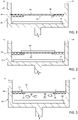
- Figures 1 to 6 show an embodiment of a production process, or manufacturing method, of a silicon-carbide wafer, in particular a 3C-SiC wafer.
- the apparatus 10 includes a reaction chamber 24, delimiting a closed space where chemical reactions of growth and doping of the SiC wafer take place.
- the apparatus 10 comprises, in a per se known manner, a heater (not illustrated), an inlet duct 16 and an outlet duct 18.
- the apparatus 10 further comprises a support 20 (also referred to as "susceptor") and a container 22, which is, for example, cup-shaped. The support 20 and the container 22 are positioned inside the reaction chamber 24.
- the heater is configured to heat the reaction chamber 24 and what is contained inside the reaction chamber 24 (for example, the support 20, the container 22, gases, substrates, wafers, or other objects or substances).
- the inlet duct 16 provides a fluidic path from the environment external to the apparatus 10 towards the reaction chamber 24 and may be used for introducing precursors and gases into the reaction chamber 24.
- the outlet duct 18 provides a fluidic path from the reaction chamber 24 towards the outside of the apparatus 10. It may also be used for discharging reaction gases formed in the reaction chamber 24 towards the outside.
- the support 20 is arranged on the container 22 and in the reaction chamber 24.
- the support 20 constitutes a platform for receiving and retaining a substrate or a wafer inside the reaction chamber 24. In particular, as discussed below, a silicon substrate is arranged on the support 20 during manufacturing of a SiC wafer.
- a substrate 58 of a first material here a silicon substrate
- a substrate 58 of a first material here a silicon substrate
- the substrate 58 is inserted into the seat 48.
- the substrate 58 has the smallest possible thickness, compatibly with characteristics of brittleness.
- the substrate 58 may have a thickness of at least 60-70 ⁇ m, in particular comprised between 200 ⁇ m and 300 ⁇ m.
- the substrate 58 generally has a crystalline structure. Moreover, in this step, the reaction chamber 24 is at room temperature.
- the reaction chamber 24 is sealed and heated by the heater to a first temperature.
- the first temperature may be comprised between 450°C and 550°C.
- a first pressure level is also set inside the reaction chamber 24, for example comprised between 8 ⁇ 10 -5 bar and 12 ⁇ 10 -5 bar.
- reaction chamber 24 After the reaction chamber 24 has been heated to the first temperature, it is brought to a second temperature, higher than the first temperature.
- the second temperature may be comprised between 1050°C and 1150°C.
- a second pressure level is also set inside the reaction chamber 24, higher than the first pressure level, for example comprised between 75 mbar and 125 mbar.
- the reaction chamber 24 is kept at the second pressure level for the rest of the process.
- the substrate 58 is immersed in hydrogen (H 2 ).
- the hydrogen is introduced into the reaction chamber 24 through the inlet duct 16.
- the substrate 58 is subjected to activation operations, by introducing hydrochloric acid (HCl) into the reaction chamber 24 through the inlet duct 16.
- the reaction chamber 10 is then heated by the heater to a third temperature, higher than the second temperature.
- the third temperature is comprised between 1340°C and 1400°C.
- a carbon-based precursor is introduced into the reaction chamber 24 through the inlet duct 16.
- the carbon-based precursor carbonizes the surface silicon atoms of the substrate 58 to form a thin SiC layer, in particular a 3C-SiC layer; in one exemplary embodiment, the thin SiC layer has a thickness of the order of a few nanometres. This step is also referred to as "ramp carbonization". As will be discussed hereinafter, this thin SiC layer acts as seed for growth of a further thicker SiC layer (in particular, of the 3C-SiC polytype).
- a silicon-based precursor is added to the carbon-based precursor in the reaction chamber 24. Consequently, a first SiC layer 60 starts to grow epitaxially from the thin SiC layer, as illustrated in Figure 2 . This step is frequently defined as "hetero-epitaxial growth".
- the first SiC layer 60 is the SiC seed layer previously mentioned.
- a melting process is carried out.
- the melting is carried out by maintaining a flow of H 2 in the reaction chamber 24 through the inlet duct 16.
- the reaction chamber 24 is heated by the heater up to a fourth temperature, higher than, or equal to, the melting temperature of the substrate 58 and lower than the melting temperature of the first SiC layer 60.
- the fourth temperature is comprised between 1550°C and 1650°C. Consequently, as illustrated in Figure 3 , the substrate 58 melts (designated by 66 in Figure 3 ) and deposits in the container 22, harvested by an absorber material 33 (e.g., a spongy material).
- the reaction chamber 24 can be kept at the fourth temperature until all the substrate 58 is removed from the first SiC layer 60, or until smaller portions or a thin residual layer 70 of the substrate 58 remain on the support 20 (the residual layer 70 of the substrate 58 is then removed by an etching process).
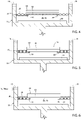
- a silicon-and-carbon-based precursor is introduced into the reaction chamber 24 through the inlet duct 16. Then, the first SiC layer 60 continues to grow in thickness or a second SiC layer 68 starts to grow on the first SiC layer 60 (e.g., by the CVD process). This step is frequently referred to as "homo-epitaxial growth".
- the silicon-and-carbon-based precursor can be supplied during the melting step of the substrate 58. Alternatively, the silicon-and-carbon-based precursor is supplied after the melting process of the substrate 58 is completed.
- the flow of the silicon-and-carbon-based precursor is stopped. Any possible reaction gases in the reaction chamber 24 are removed from the reaction chamber 24 through the outlet duct 18.
- the SiC wafer contains residual portions 70 of the substrate 58, these can be removed by an etching process during growth of the second SiC layer 68 or at the end of said growth.
- an etching chemistry in particular in gaseous form
- hydrochloric acid (HCl) is introduced into the reaction chamber 24 through the inlet duct 16, which acts by removing the residual portions 70, which in turn are extracted from the chamber 24 through the outlet duct 18.
- the SiC wafer 72 has a diameter comprised between 2 and 12 inches, in particular 6 inches.
- the SiC wafer 72 can be used, for example, as a substrate for the manufacturing of electronic devices (e.g., by growing further layers on it and /or carrying out steps of dopant implantations and activations, lithography, etc.).
- doping of the SiC layer 68 is carried out during the step of CVD growth.
- This aspect of the invention is illustrated in Figure 6 , which reproduces the step of Figure 4 .
- Doping here has the dual function of setting a desired value of electrical resistivity of the wafer 72 as a function of subsequent steps of formation of electronic components, and of regulating a net stress value to which the SiC wafer 72 is subject at the end of the manufacturing steps.
- the doping process of the second SiC layer 69 is carried out by simultaneously providing, during CVD growth, two different dopant species, one of which is an N type and one is a P type; the dopant species are, for example, provided by using precursors in the gaseous phase, such as nitrogen (N 2 ) for a doping of an N type, and trimethyl aluminium, TMA or Al 2 (CH 3 ) 6 , for a doping of a P type by aluminium atoms.
- the provision of the two different dopant species may not be simultaneous but in any case such that, at a certain point in time of the CVD growth, both dopant species are present in the reaction chamber used for sich CVD growth.
- the present applicant has found that, by appropriately calibrating the concentrations of N and P dopants in the SiC wafer 72 (or, equivalently, the dose of dopant or precursor introduced into the reaction chamber) it is possible to regulate the tensile and compressive stresses of the SiC wafer 72.
- the compressive and tensile stresses act in a direction orthogonal to the defined plane of the surface of the SiC wafer 72 and tend to bend it in mutually opposite directions.
- N 2 enables regulation of the stress in a compressive direction (it acts in a first direction)
- P type carried out by TMA enables regulation of the stress in a tensile direction (it acts in a second direction parallel and opposite to the first direction).
- the desired stress balancing is obtained by introducing, into the reaction chamber 24, precursors in the gaseous phase with a flow, measured in sccm (standard cubic centimetres per minute), that respects the following proportion.
- a flow of nitrogen equal to "x" sccm, chosen as a function of the doping of an N type that it is desired to obtain in the SiC wafer 72, the flow "y" of TMA is comprised between 0.01% and 1% of the value of x.
- the values of x may range between 500 and 1800 sccm, and the values of y may range between 0.1 and 5 sccm, these values being chosen so as to respect the aforementioned proportion.
- flow values may vary as a function of the size of the reaction chamber used and/or of the desired dopant concentration at the level of the SiC wafer 72.
- the Applicant verified that the N-type dopant (N 2 ) concentration can be set in the range 10 18 atoms/cm 3 - 10 20 atoms/cm 3 , and the P-type dopants (Al) concentration can be set in the range 10 17 atoms/cm 3 - 10 19 atoms/cm 3 .
- substantially flat wafers 72 can be obtained with N-type dopant concentration in the range 2 ⁇ 10 19 atoms/cm 3 - 6 ⁇ 10 19 atoms/cm 3 , and P-type dopant concentration in the range 1.5 ⁇ 10 18 atoms/cm 3 - 7 ⁇ 10 18 atoms/cm 3 .
- the balance of the stress using the above values is particularly effective with 3C-SiC.
- the concentration of dopants can, in general, vary according to the electrical requirements of the wafer thus manufactured. For instance, to obtain a SiC wafer 72 with a net doping of an N type, measured at the level of the SiC wafer 72, of the order of 10 18 atoms/cm 3 , the concentration of N dopants measured at the level of the wafer 72 is between 4 ⁇ 10 18 and 1.5 ⁇ 10 19 atoms/cm 3 and the concentration of P dopants measured at the level of the wafer 72 is higher than 10 17 atoms/cm 3 (e.g., 1 ⁇ 10 18 atoms/cm 3 ) and lower than 10 19 atoms/cm 3 (e.g., 8 ⁇ 10 18 atoms/cm 3 ).
- the manufacturing process described above is carried out in the same the reaction chamber 24, in particular without removing from the reaction chamber 24 the product under manufacturing (i.e., the SiC wafer 72 and its intermediate products formed by the stack of two or more among substrate 58, layer 60 and layer 68).
- the product under manufacturing i.e., the SiC wafer 72 and its intermediate products formed by the stack of two or more among substrate 58, layer 60 and layer 68.
- the Applicant found that in case the SiC wafer 72 (or its intermediate products) is removed from the reaction chamber 24 during an intermediate step of manufacturing, there is a high risk of breackage of the SiC wafer 72 (or of its intermediate products).
- any of the stacks formed with reference to Figures 2 to 4 is removed from the reaction chamber 24 to perform a step of removal of the substrate 58 (e.g., using a delamination process), such stack would most probably break or crack during the removal process.
- a process of melting the substrate 58 in the reaction chamber 24 as discussed with reference to Figure 3 and, if necessary, completing the process by the etching step discussed with reference to Figure 4 , layers 60 and 68 are not compromised and the SiC wafer 72 thus obtained does not show cracks or other physical damages.
- teaching of the present invention likewise applies for obtaining a net doping of a P type on the SiC wafer, balancing the effect of the stress by introduction of dopant species of an N type.
- dopant species alternative to nitrogen may be used, for example phosphorus (P); for a doping of a P type, dopant species alternative to aluminium may be used, for example boron (B).
- P phosphorus
- B boron
Landscapes
- Crystals, And After-Treatments Of Crystals (AREA)
- Recrystallisation Techniques (AREA)
- Chemical Vapour Deposition (AREA)
- Carbon And Carbon Compounds (AREA)
- Ceramic Products (AREA)
Applications Claiming Priority (1)
| Application Number | Priority Date | Filing Date | Title |
|---|---|---|---|
| IT102020000028778A IT202000028778A1 (it) | 2020-11-27 | 2020-11-27 | Procedimento di fabbricazione di una fetta di sic con controllo dello stress residuo |
Publications (3)
| Publication Number | Publication Date |
|---|---|
| EP4006954A1 true EP4006954A1 (fr) | 2022-06-01 |
| EP4006954C0 EP4006954C0 (fr) | 2026-03-18 |
| EP4006954B1 EP4006954B1 (fr) | 2026-03-18 |
Family
ID=74557191
Family Applications (1)
| Application Number | Title | Priority Date | Filing Date |
|---|---|---|---|
| EP21210770.0A Active EP4006954B1 (fr) | 2020-11-27 | 2021-11-26 | Procédé de fabrication d'une tranche de sic avec commande de la contrainte résiduelle |
Country Status (4)
| Country | Link |
|---|---|
| US (1) | US20220172949A1 (fr) |
| EP (1) | EP4006954B1 (fr) |
| JP (1) | JP2022085874A (fr) |
| IT (1) | IT202000028778A1 (fr) |
Cited By (1)
| Publication number | Priority date | Publication date | Assignee | Title |
|---|---|---|---|---|
| GB2613871B (en) * | 2021-12-17 | 2024-12-04 | Anvil Semiconductors Ltd | Reducing electrical activity of defects in silicon carbide grown on silicon |
Families Citing this family (1)
| Publication number | Priority date | Publication date | Assignee | Title |
|---|---|---|---|---|
| IT201900015416A1 (it) * | 2019-09-03 | 2021-03-03 | St Microelectronics Srl | Apparecchio per la crescita di una fetta di materiale semiconduttore, in particolare di carburo di silicio, e procedimento di fabbricazione associato |
Citations (5)
| Publication number | Priority date | Publication date | Assignee | Title |
|---|---|---|---|---|
| EP2604729A1 (fr) * | 2011-12-15 | 2013-06-19 | STMicroelectronics Srl | Procédé de fabrication d'une plaquette en carbure de silicium et équipement correspondant |
| EP2782117A1 (fr) | 2013-03-22 | 2014-09-24 | Kabushiki Kaisha Toshiba | Tranche épitaxiale au SiC et dispositif semi-conducteur |
| US20180090350A1 (en) | 2016-09-28 | 2018-03-29 | Stmicroelectronics S.R.L. | Apparatus for manufacturing a silicon carbide wafer |
| US20200144047A1 (en) | 2018-11-06 | 2020-05-07 | Stmicroelectronics S.R.L. | Apparatus and method for manufacturing a wafer |
| US20200357637A1 (en) * | 2019-05-08 | 2020-11-12 | Infineon Technologies Ag | Method of Manufacturing a Silicon Carbide Device and Wafer Composite Including Laser Modified Zones in a Handle Substrate |
Family Cites Families (6)
| Publication number | Priority date | Publication date | Assignee | Title |
|---|---|---|---|---|
| US6067680A (en) * | 1998-04-29 | 2000-05-30 | Micron Technology, Inc. | Semiconductor processing method of forming a conductively doped semiconductive material plug within a contact opening |
| JP5794276B2 (ja) * | 2013-11-01 | 2015-10-14 | トヨタ自動車株式会社 | n型SiC単結晶およびその用途 |
| JP6753705B2 (ja) * | 2016-06-10 | 2020-09-09 | エア・ウォーター株式会社 | 基板の製造方法 |
| JP6340642B2 (ja) * | 2017-04-25 | 2018-06-13 | 住友電気工業株式会社 | 炭化珪素半導体基板およびその製造方法、ならびに炭化珪素半導体装置の製造方法 |
| CN110923659B (zh) * | 2018-09-20 | 2022-07-08 | 东京毅力科创株式会社 | 成膜方法及基板处理系统 |
| EP4243054A4 (fr) * | 2020-11-09 | 2024-11-13 | NuFlare Technology, Inc. | Appareil de croissance en phase vapeur |
-
2020
- 2020-11-27 IT IT102020000028778A patent/IT202000028778A1/it unknown
-
2021
- 2021-11-22 JP JP2021189317A patent/JP2022085874A/ja active Pending
- 2021-11-23 US US17/534,156 patent/US20220172949A1/en active Pending
- 2021-11-26 EP EP21210770.0A patent/EP4006954B1/fr active Active
Patent Citations (5)
| Publication number | Priority date | Publication date | Assignee | Title |
|---|---|---|---|---|
| EP2604729A1 (fr) * | 2011-12-15 | 2013-06-19 | STMicroelectronics Srl | Procédé de fabrication d'une plaquette en carbure de silicium et équipement correspondant |
| EP2782117A1 (fr) | 2013-03-22 | 2014-09-24 | Kabushiki Kaisha Toshiba | Tranche épitaxiale au SiC et dispositif semi-conducteur |
| US20180090350A1 (en) | 2016-09-28 | 2018-03-29 | Stmicroelectronics S.R.L. | Apparatus for manufacturing a silicon carbide wafer |
| US20200144047A1 (en) | 2018-11-06 | 2020-05-07 | Stmicroelectronics S.R.L. | Apparatus and method for manufacturing a wafer |
| US20200357637A1 (en) * | 2019-05-08 | 2020-11-12 | Infineon Technologies Ag | Method of Manufacturing a Silicon Carbide Device and Wafer Composite Including Laser Modified Zones in a Handle Substrate |
Non-Patent Citations (3)
| Title |
|---|
| GUBANOV V A ET AL: "Doping in cubic silicon-carbide", APPLIED PHYSICS LETTERS, A I P PUBLISHING LLC, US, vol. 75, no. 1, 5 July 1999 (1999-07-05), pages 88 - 90, XP012023423, ISSN: 0003-6951, DOI: 10.1063/1.124285 * |
| SU JIAN-FENG ET AL: "CONDENSED MATTER: STRUCTURE, MECHANICAL, AND THERMAL PROPERTIES; Effect of Al Doping on Properties of SiC Films", CHINESE PHYSICS LETTERS, INSTITUTE OF PHYSICS PUBLISHING, BRISTOL, GB, vol. 25, no. 9, 1 September 2008 (2008-09-01), pages 3346 - 3349, XP020142057, ISSN: 0256-307X * |
| SUN J ET AL: "Combined effects of Ga, N, and Al codoping in solution grown 3C-SiC", JOURNAL OF APPLIED PHYSICS, AMERICAN INSTITUTE OF PHYSICS, US, vol. 108, no. 1, 1 July 2010 (2010-07-01), pages 13503 - 13503, XP012141738, ISSN: 0021-8979, DOI: 10.1063/1.3455999 * |
Cited By (1)
| Publication number | Priority date | Publication date | Assignee | Title |
|---|---|---|---|---|
| GB2613871B (en) * | 2021-12-17 | 2024-12-04 | Anvil Semiconductors Ltd | Reducing electrical activity of defects in silicon carbide grown on silicon |
Also Published As
| Publication number | Publication date |
|---|---|
| JP2022085874A (ja) | 2022-06-08 |
| EP4006954C0 (fr) | 2026-03-18 |
| IT202000028778A1 (it) | 2022-05-27 |
| EP4006954B1 (fr) | 2026-03-18 |
| US20220172949A1 (en) | 2022-06-02 |
Similar Documents
| Publication | Publication Date | Title |
|---|---|---|
| CN110268104B (zh) | 稳定的高掺杂碳化硅 | |
| CN101072901B (zh) | 制造高品质大尺寸碳化硅晶体的方法 | |
| EP2584071B1 (fr) | Wafer en carbure de silicium de 3 pouces ayant une faible concentration en dislocation vis de type 1c | |
| TWI770769B (zh) | 使用得自聚合物之高純度碳化矽之氣相沉積設備與技術 | |
| KR100450316B1 (ko) | 탄화 규소 및 이의 제조 방법 | |
| EP2044244B1 (fr) | Procédé de fabrication de substrats à durée de vie de porteurs améliorée | |
| EP1807558A2 (fr) | Plaquette en carbure de silicium 100mm a faible densité de microtubes | |
| EP4006954B1 (fr) | Procédé de fabrication d'une tranche de sic avec commande de la contrainte résiduelle | |
| CN109628998B (zh) | 碳化硅晶体及其制造方法 | |
| KR20110021986A (ko) | 반도체 에피텍시에서 메모리 효과들을 감소시키는 방법 | |
| JP7322594B2 (ja) | 炭化珪素基板及びその製造方法 | |
| EP2704183A2 (fr) | Procédé de fabrication de dispositif semi-conducteur au carbure de silicium | |
| JP2004343133A (ja) | 炭化珪素製造方法、炭化珪素及び半導体装置 | |
| CN114561705B (zh) | 具有残余应力控制的SiC晶片的制造方法 | |
| JP7392526B2 (ja) | 炭化ケイ素単結晶基板の製造方法 | |
| JP7247819B2 (ja) | 炭化ケイ素多結晶基板の製造方法 | |
| KR101936170B1 (ko) | 탄화규소 에피 웨이퍼 제조 방법 | |
| CN108699726B (zh) | 由碳化硅构成的半导体基板及其制造方法 | |
| US9991344B2 (en) | Silicon carbide EPI wafer and method for manufacturing same | |
| Pessoa et al. | Low-pressure deposition techniques of silicon carbide thin films: An overview | |
| KR102417484B1 (ko) | 에피택셜 웨이퍼 및 그 제조 방법 | |
| CN120465103A (zh) | 一种3c型碳化硅多晶体基板及其制备方法和应用 | |
| KR101742210B1 (ko) | 탄화규소 에피 박막 성장 방법 | |
| JP2019147996A (ja) | 単一CVD−SiC及びその製造方法 |
Legal Events
| Date | Code | Title | Description |
|---|---|---|---|
| PUAI | Public reference made under article 153(3) epc to a published international application that has entered the european phase |
Free format text: ORIGINAL CODE: 0009012 |
|
| STAA | Information on the status of an ep patent application or granted ep patent |
Free format text: STATUS: THE APPLICATION HAS BEEN PUBLISHED |
|
| AK | Designated contracting states |
Kind code of ref document: A1 Designated state(s): AL AT BE BG CH CY CZ DE DK EE ES FI FR GB GR HR HU IE IS IT LI LT LU LV MC MK MT NL NO PL PT RO RS SE SI SK SM TR |
|
| STAA | Information on the status of an ep patent application or granted ep patent |
Free format text: STATUS: REQUEST FOR EXAMINATION WAS MADE |
|
| 17P | Request for examination filed |
Effective date: 20221124 |
|
| RBV | Designated contracting states (corrected) |
Designated state(s): AL AT BE BG CH CY CZ DE DK EE ES FI FR GB GR HR HU IE IS IT LI LT LU LV MC MK MT NL NO PL PT RO RS SE SI SK SM TR |
|
| STAA | Information on the status of an ep patent application or granted ep patent |
Free format text: STATUS: EXAMINATION IS IN PROGRESS |
|
| 17Q | First examination report despatched |
Effective date: 20240730 |
|
| REG | Reference to a national code |
Ref country code: DE Ref legal event code: R079 Free format text: PREVIOUS MAIN CLASS: H01L0021020000 Ipc: H01L0021200000 Ref country code: DE Ref legal event code: R079 Ref document number: 602021050096 Country of ref document: DE Free format text: PREVIOUS MAIN CLASS: H01L0021020000 Ipc: H01L0021200000 |
|
| GRAP | Despatch of communication of intention to grant a patent |
Free format text: ORIGINAL CODE: EPIDOSNIGR1 |
|
| STAA | Information on the status of an ep patent application or granted ep patent |
Free format text: STATUS: GRANT OF PATENT IS INTENDED |
|
| RIC1 | Information provided on ipc code assigned before grant |
Ipc: H01L 21/20 20060101AFI20251009BHEP |
|
| INTG | Intention to grant announced |
Effective date: 20251016 |
|
| GRAS | Grant fee paid |
Free format text: ORIGINAL CODE: EPIDOSNIGR3 |
|
| GRAA | (expected) grant |
Free format text: ORIGINAL CODE: 0009210 |
|
| STAA | Information on the status of an ep patent application or granted ep patent |
Free format text: STATUS: THE PATENT HAS BEEN GRANTED |
|
| AK | Designated contracting states |
Kind code of ref document: B1 Designated state(s): AL AT BE BG CH CY CZ DE DK EE ES FI FR GB GR HR HU IE IS IT LI LT LU LV MC MK MT NL NO PL PT RO RS SE SI SK SM TR |
|
| REG | Reference to a national code |
Ref country code: CH Ref legal event code: F10 Free format text: ST27 STATUS EVENT CODE: U-0-0-F10-F00 (AS PROVIDED BY THE NATIONAL OFFICE) Effective date: 20260318 Ref country code: GB Ref legal event code: FG4D |
|
| REG | Reference to a national code |
Ref country code: IE Ref legal event code: FG4D |
|
| U01 | Request for unitary effect filed |
Effective date: 20260318 |
|
| U07 | Unitary effect registered |
Designated state(s): AT BE BG DE DK EE FI FR IT LT LU LV MT NL PT RO SE SI Effective date: 20260324 |