EP4006983A1 - Substrat d'affichage et son procédé de préparation, panneau d'affichage et appareil d'affichage - Google Patents
Substrat d'affichage et son procédé de préparation, panneau d'affichage et appareil d'affichage Download PDFInfo
- Publication number
- EP4006983A1 EP4006983A1 EP19933238.8A EP19933238A EP4006983A1 EP 4006983 A1 EP4006983 A1 EP 4006983A1 EP 19933238 A EP19933238 A EP 19933238A EP 4006983 A1 EP4006983 A1 EP 4006983A1
- Authority
- EP
- European Patent Office
- Prior art keywords
- pixel
- light
- sub
- circuit
- emitting
- Prior art date
- Legal status (The legal status is an assumption and is not a legal conclusion. Google has not performed a legal analysis and makes no representation as to the accuracy of the status listed.)
- Granted
Links
Images



Classifications
-
- H—ELECTRICITY
- H10—SEMICONDUCTOR DEVICES; ELECTRIC SOLID-STATE DEVICES NOT OTHERWISE PROVIDED FOR
- H10K—ORGANIC ELECTRIC SOLID-STATE DEVICES
- H10K59/00—Integrated devices, or assemblies of multiple devices, comprising at least one organic light-emitting element covered by group H10K50/00
- H10K59/30—Devices specially adapted for multicolour light emission
- H10K59/35—Devices specially adapted for multicolour light emission comprising red-green-blue [RGB] subpixels
- H10K59/351—Devices specially adapted for multicolour light emission comprising red-green-blue [RGB] subpixels comprising more than three subpixels, e.g. red-green-blue-white [RGBW]
-
- G—PHYSICS
- G09—EDUCATION; CRYPTOGRAPHY; DISPLAY; ADVERTISING; SEALS
- G09G—ARRANGEMENTS OR CIRCUITS FOR CONTROL OF INDICATING DEVICES USING STATIC MEANS TO PRESENT VARIABLE INFORMATION
- G09G3/00—Control arrangements or circuits, of interest only in connection with visual indicators other than cathode-ray tubes
- G09G3/20—Control arrangements or circuits, of interest only in connection with visual indicators other than cathode-ray tubes for presentation of an assembly of a number of characters, e.g. a page, by composing the assembly by combination of individual elements arranged in a matrix no fixed position being assigned to or needed to be assigned to the individual characters or partial characters
- G09G3/22—Control arrangements or circuits, of interest only in connection with visual indicators other than cathode-ray tubes for presentation of an assembly of a number of characters, e.g. a page, by composing the assembly by combination of individual elements arranged in a matrix no fixed position being assigned to or needed to be assigned to the individual characters or partial characters using controlled light sources
- G09G3/30—Control arrangements or circuits, of interest only in connection with visual indicators other than cathode-ray tubes for presentation of an assembly of a number of characters, e.g. a page, by composing the assembly by combination of individual elements arranged in a matrix no fixed position being assigned to or needed to be assigned to the individual characters or partial characters using controlled light sources using electroluminescent panels
- G09G3/32—Control arrangements or circuits, of interest only in connection with visual indicators other than cathode-ray tubes for presentation of an assembly of a number of characters, e.g. a page, by composing the assembly by combination of individual elements arranged in a matrix no fixed position being assigned to or needed to be assigned to the individual characters or partial characters using controlled light sources using electroluminescent panels semiconductive, e.g. using light-emitting diodes [LED]
- G09G3/3208—Control arrangements or circuits, of interest only in connection with visual indicators other than cathode-ray tubes for presentation of an assembly of a number of characters, e.g. a page, by composing the assembly by combination of individual elements arranged in a matrix no fixed position being assigned to or needed to be assigned to the individual characters or partial characters using controlled light sources using electroluminescent panels semiconductive, e.g. using light-emitting diodes [LED] organic, e.g. using organic light-emitting diodes [OLED]
- G09G3/3225—Control arrangements or circuits, of interest only in connection with visual indicators other than cathode-ray tubes for presentation of an assembly of a number of characters, e.g. a page, by composing the assembly by combination of individual elements arranged in a matrix no fixed position being assigned to or needed to be assigned to the individual characters or partial characters using controlled light sources using electroluminescent panels semiconductive, e.g. using light-emitting diodes [LED] organic, e.g. using organic light-emitting diodes [OLED] using an active matrix
- G09G3/3233—Control arrangements or circuits, of interest only in connection with visual indicators other than cathode-ray tubes for presentation of an assembly of a number of characters, e.g. a page, by composing the assembly by combination of individual elements arranged in a matrix no fixed position being assigned to or needed to be assigned to the individual characters or partial characters using controlled light sources using electroluminescent panels semiconductive, e.g. using light-emitting diodes [LED] organic, e.g. using organic light-emitting diodes [OLED] using an active matrix with pixel circuitry controlling the current through the light-emitting element
-
- H—ELECTRICITY
- H10—SEMICONDUCTOR DEVICES; ELECTRIC SOLID-STATE DEVICES NOT OTHERWISE PROVIDED FOR
- H10K—ORGANIC ELECTRIC SOLID-STATE DEVICES
- H10K59/00—Integrated devices, or assemblies of multiple devices, comprising at least one organic light-emitting element covered by group H10K50/00
- H10K59/10—OLED displays
- H10K59/12—Active-matrix OLED [AMOLED] displays
- H10K59/121—Active-matrix OLED [AMOLED] displays characterised by the geometry or disposition of pixel elements
- H10K59/1213—Active-matrix OLED [AMOLED] displays characterised by the geometry or disposition of pixel elements the pixel elements being TFTs
-
- H—ELECTRICITY
- H10—SEMICONDUCTOR DEVICES; ELECTRIC SOLID-STATE DEVICES NOT OTHERWISE PROVIDED FOR
- H10K—ORGANIC ELECTRIC SOLID-STATE DEVICES
- H10K59/00—Integrated devices, or assemblies of multiple devices, comprising at least one organic light-emitting element covered by group H10K50/00
- H10K59/10—OLED displays
- H10K59/12—Active-matrix OLED [AMOLED] displays
- H10K59/122—Pixel-defining structures or layers, e.g. banks
-
- H—ELECTRICITY
- H10—SEMICONDUCTOR DEVICES; ELECTRIC SOLID-STATE DEVICES NOT OTHERWISE PROVIDED FOR
- H10K—ORGANIC ELECTRIC SOLID-STATE DEVICES
- H10K59/00—Integrated devices, or assemblies of multiple devices, comprising at least one organic light-emitting element covered by group H10K50/00
- H10K59/10—OLED displays
- H10K59/12—Active-matrix OLED [AMOLED] displays
- H10K59/123—Connection of the pixel electrodes to the thin film transistors [TFT]
-
- H—ELECTRICITY
- H10—SEMICONDUCTOR DEVICES; ELECTRIC SOLID-STATE DEVICES NOT OTHERWISE PROVIDED FOR
- H10K—ORGANIC ELECTRIC SOLID-STATE DEVICES
- H10K59/00—Integrated devices, or assemblies of multiple devices, comprising at least one organic light-emitting element covered by group H10K50/00
- H10K59/10—OLED displays
- H10K59/12—Active-matrix OLED [AMOLED] displays
- H10K59/131—Interconnections, e.g. wiring lines or terminals
-
- H—ELECTRICITY
- H10—SEMICONDUCTOR DEVICES; ELECTRIC SOLID-STATE DEVICES NOT OTHERWISE PROVIDED FOR
- H10K—ORGANIC ELECTRIC SOLID-STATE DEVICES
- H10K59/00—Integrated devices, or assemblies of multiple devices, comprising at least one organic light-emitting element covered by group H10K50/00
- H10K59/10—OLED displays
- H10K59/12—Active-matrix OLED [AMOLED] displays
- H10K59/131—Interconnections, e.g. wiring lines or terminals
- H10K59/1315—Interconnections, e.g. wiring lines or terminals comprising structures specially adapted for lowering the resistance
-
- H—ELECTRICITY
- H10—SEMICONDUCTOR DEVICES; ELECTRIC SOLID-STATE DEVICES NOT OTHERWISE PROVIDED FOR
- H10K—ORGANIC ELECTRIC SOLID-STATE DEVICES
- H10K59/00—Integrated devices, or assemblies of multiple devices, comprising at least one organic light-emitting element covered by group H10K50/00
- H10K59/30—Devices specially adapted for multicolour light emission
- H10K59/35—Devices specially adapted for multicolour light emission comprising red-green-blue [RGB] subpixels
- H10K59/352—Devices specially adapted for multicolour light emission comprising red-green-blue [RGB] subpixels the areas of the RGB subpixels being different
-
- H—ELECTRICITY
- H10—SEMICONDUCTOR DEVICES; ELECTRIC SOLID-STATE DEVICES NOT OTHERWISE PROVIDED FOR
- H10K—ORGANIC ELECTRIC SOLID-STATE DEVICES
- H10K59/00—Integrated devices, or assemblies of multiple devices, comprising at least one organic light-emitting element covered by group H10K50/00
- H10K59/30—Devices specially adapted for multicolour light emission
- H10K59/35—Devices specially adapted for multicolour light emission comprising red-green-blue [RGB] subpixels
- H10K59/353—Devices specially adapted for multicolour light emission comprising red-green-blue [RGB] subpixels characterised by the geometrical arrangement of the RGB subpixels
-
- G—PHYSICS
- G09—EDUCATION; CRYPTOGRAPHY; DISPLAY; ADVERTISING; SEALS
- G09G—ARRANGEMENTS OR CIRCUITS FOR CONTROL OF INDICATING DEVICES USING STATIC MEANS TO PRESENT VARIABLE INFORMATION
- G09G2300/00—Aspects of the constitution of display devices
- G09G2300/04—Structural and physical details of display devices
- G09G2300/0421—Structural details of the set of electrodes
- G09G2300/0426—Layout of electrodes and connections
-
- G—PHYSICS
- G09—EDUCATION; CRYPTOGRAPHY; DISPLAY; ADVERTISING; SEALS
- G09G—ARRANGEMENTS OR CIRCUITS FOR CONTROL OF INDICATING DEVICES USING STATIC MEANS TO PRESENT VARIABLE INFORMATION
- G09G2300/00—Aspects of the constitution of display devices
- G09G2300/04—Structural and physical details of display devices
- G09G2300/0439—Pixel structures
- G09G2300/0443—Pixel structures with several sub-pixels for the same colour in a pixel, not specifically used to display gradations
-
- G—PHYSICS
- G09—EDUCATION; CRYPTOGRAPHY; DISPLAY; ADVERTISING; SEALS
- G09G—ARRANGEMENTS OR CIRCUITS FOR CONTROL OF INDICATING DEVICES USING STATIC MEANS TO PRESENT VARIABLE INFORMATION
- G09G2300/00—Aspects of the constitution of display devices
- G09G2300/04—Structural and physical details of display devices
- G09G2300/0439—Pixel structures
- G09G2300/0452—Details of colour pixel setup, e.g. pixel composed of a red, a blue and two green components
-
- G—PHYSICS
- G09—EDUCATION; CRYPTOGRAPHY; DISPLAY; ADVERTISING; SEALS
- G09G—ARRANGEMENTS OR CIRCUITS FOR CONTROL OF INDICATING DEVICES USING STATIC MEANS TO PRESENT VARIABLE INFORMATION
- G09G2300/00—Aspects of the constitution of display devices
- G09G2300/08—Active matrix structure, i.e. with use of active elements, inclusive of non-linear two terminal elements, in the pixels together with light emitting or modulating elements
- G09G2300/0809—Several active elements per pixel in active matrix panels
- G09G2300/0819—Several active elements per pixel in active matrix panels used for counteracting undesired variations, e.g. feedback or autozeroing
-
- G—PHYSICS
- G09—EDUCATION; CRYPTOGRAPHY; DISPLAY; ADVERTISING; SEALS
- G09G—ARRANGEMENTS OR CIRCUITS FOR CONTROL OF INDICATING DEVICES USING STATIC MEANS TO PRESENT VARIABLE INFORMATION
- G09G2300/00—Aspects of the constitution of display devices
- G09G2300/08—Active matrix structure, i.e. with use of active elements, inclusive of non-linear two terminal elements, in the pixels together with light emitting or modulating elements
- G09G2300/0809—Several active elements per pixel in active matrix panels
- G09G2300/0842—Several active elements per pixel in active matrix panels forming a memory circuit, e.g. a dynamic memory with one capacitor
- G09G2300/0852—Several active elements per pixel in active matrix panels forming a memory circuit, e.g. a dynamic memory with one capacitor being a dynamic memory with more than one capacitor
-
- G—PHYSICS
- G09—EDUCATION; CRYPTOGRAPHY; DISPLAY; ADVERTISING; SEALS
- G09G—ARRANGEMENTS OR CIRCUITS FOR CONTROL OF INDICATING DEVICES USING STATIC MEANS TO PRESENT VARIABLE INFORMATION
- G09G2320/00—Control of display operating conditions
- G09G2320/02—Improving the quality of display appearance
- G09G2320/0233—Improving the luminance or brightness uniformity across the screen
-
- H—ELECTRICITY
- H10—SEMICONDUCTOR DEVICES; ELECTRIC SOLID-STATE DEVICES NOT OTHERWISE PROVIDED FOR
- H10D—INORGANIC ELECTRIC SEMICONDUCTOR DEVICES
- H10D86/00—Integrated devices formed in or on insulating or conducting substrates, e.g. formed in silicon-on-insulator [SOI] substrates or on stainless steel or glass substrates
- H10D86/40—Integrated devices formed in or on insulating or conducting substrates, e.g. formed in silicon-on-insulator [SOI] substrates or on stainless steel or glass substrates characterised by multiple TFTs
- H10D86/441—Interconnections, e.g. scanning lines
-
- H—ELECTRICITY
- H10—SEMICONDUCTOR DEVICES; ELECTRIC SOLID-STATE DEVICES NOT OTHERWISE PROVIDED FOR
- H10D—INORGANIC ELECTRIC SEMICONDUCTOR DEVICES
- H10D86/00—Integrated devices formed in or on insulating or conducting substrates, e.g. formed in silicon-on-insulator [SOI] substrates or on stainless steel or glass substrates
- H10D86/40—Integrated devices formed in or on insulating or conducting substrates, e.g. formed in silicon-on-insulator [SOI] substrates or on stainless steel or glass substrates characterised by multiple TFTs
- H10D86/60—Integrated devices formed in or on insulating or conducting substrates, e.g. formed in silicon-on-insulator [SOI] substrates or on stainless steel or glass substrates characterised by multiple TFTs wherein the TFTs are in active matrices
-
- H—ELECTRICITY
- H10—SEMICONDUCTOR DEVICES; ELECTRIC SOLID-STATE DEVICES NOT OTHERWISE PROVIDED FOR
- H10K—ORGANIC ELECTRIC SOLID-STATE DEVICES
- H10K59/00—Integrated devices, or assemblies of multiple devices, comprising at least one organic light-emitting element covered by group H10K50/00
- H10K59/80—Constructional details
- H10K59/805—Electrodes
- H10K59/8051—Anodes
- H10K59/80515—Anodes characterised by their shape
Definitions
- Embodiments of the present disclosure relate to a display substrate, a preparation method thereof, a display panel, and a display device.
- AMOLED active-matrix organic light-emitting diode
- the display substrate includes a base substrate and a plurality of repeating units on the base substrate, each of the plurality of repeating units comprises a plurality of sub-pixels, and each of the plurality of sub-pixels comprises a light-emitting element and a pixel circuit for driving the light-emitting element to emit light;
- the pixel circuit comprises a drive circuit;
- the light-emitting element comprises a first light-emitting voltage application electrode, a second light-emitting voltage application electrode, and a light-emitting layer between the first light-emitting voltage application electrode and the second light-emitting voltage application electrode;
- the plurality of sub-pixels comprise a first sub-pixel and a second sub-pixel, a color of light emitted by the light-emitting element of the first sub-pixel is identical to a color of light emitted by the light-emitting element of the second sub-pixel, and a shape of the first light-emitting voltage application
- an area of the orthographic projection of the first light-emitting voltage application electrode of the light-emitting element of the first sub-pixel on the base substrate is different from an area of the orthographic projection of the first light-emitting voltage application electrode of the light-emitting element of the second sub-pixel on the base substrate.
- an area of an overlapping portion between the orthographic projection of the control terminal of the drive circuit of the pixel circuit of the first sub-pixel on the base substrate and the orthographic projection of the first light-emitting voltage application electrode of the light-emitting element of the first sub-pixel on the base substrate is a first area
- an area of an overlapping portion between the orthographic projection of the control terminal of the drive circuit of the pixel circuit of the second sub-pixel on the base substrate and the orthographic projection of the first light-emitting voltage application electrode of the light-emitting element of the second sub-pixel on the base substrate is a second area
- a ratio of the first area to the second area satisfies a following relation: Amin ⁇ A 1 /A 2 ⁇ Amax , where A1 represents the first area, A2 represents the second area, Amin represents a minimum ratio threshold and is 90%, and Amax represents a maximum ratio threshold and is 110%.
- the orthographic projection of the control terminal of the drive circuit of the pixel circuit of the first sub-pixel on the base substrate is within the orthographic projection of the first light-emitting voltage application electrode of the light-emitting element of the first sub-pixel on the base substrate; and the orthographic projection of the control terminal of the drive circuit of the pixel circuit of the second sub-pixel on the base substrate is within the orthographic projection of the first light-emitting voltage application electrode of the light-emitting element of the second sub-pixel on the base substrate.
- an orthographic projection of the light-emitting layer of the light-emitting element of the first sub-pixel on the base substrate is continuous with an orthographic projection of the light-emitting layer of the light-emitting element of the second sub-pixel on the base substrate.
- the pixel circuit further comprises a first light-emitting control circuit and a second light-emitting control circuit
- the drive circuit comprises a control terminal, a first terminal, and a second terminal
- the drive circuit is configured to provide a drive current for driving the light-emitting element to emit light
- the first light-emitting control circuit is connected to the first terminal of the drive circuit and a first voltage terminal
- the first light-emitting control circuit is configured to turn on or turn off a connection between the drive circuit and the first voltage terminal
- the second light-emitting control circuit is electrically connected to the second terminal of the drive circuit and the first light-emitting voltage application electrode of the light-emitting element, and the second light-emitting control circuit is configured to turn on or turn off a connection between the drive circuit and the light-emitting element.
- the pixel circuit of the first sub-pixel further comprises a first parasitic circuit
- the pixel circuit of the second sub-pixel further comprises a second parasitic circuit
- the first parasitic circuit is electrically connected to the control terminal of the drive circuit of the pixel circuit of the first sub-pixel and the first light-emitting voltage application electrode of the light-emitting element of the first sub-pixel
- the first parasitic circuit is configured to control a voltage of the control terminal of the drive circuit of the pixel circuit of the first sub-pixel based on a voltage of the first light-emitting voltage application electrode of the light-emitting element of the first sub-pixel
- the second parasitic circuit is electrically connected to the control terminal of the drive circuit of the pixel circuit of the second sub-pixel and the first light-emitting voltage application electrode of the light-emitting element of the second sub-pixel, and the second parasitic circuit is configured to control a voltage of the control terminal of the drive circuit of the pixel circuit
- the first parasitic circuit comprises a first capacitor, and the first capacitor comprises a first electrode and a second electrode; the first light-emitting voltage application electrode of the light-emitting element of the first sub-pixel comprises an auxiliary electrode block, and an orthographic projection of the auxiliary electrode block on the base substrate at least partially overlaps with the orthographic projection of the control terminal of the drive circuit of the pixel circuit of the first sub-pixel on the base substrate; and the auxiliary electrode block serves as the first electrode of the first capacitor, and the control terminal of the drive circuit of the first sub-pixel is multiplexed as the second electrode of the first capacitor.
- the first light-emitting voltage application electrode of the light-emitting element of the first sub-pixel further comprises a first drive electrode block, and the first drive electrode block is electrically connected to the auxiliary electrode block, and an orthographic projection of the first drive electrode block on the base substrate, the orthographic projection of the light-emitting layer of the light-emitting element of the first sub-pixel on the base substrate, and the orthographic projection of the second light-emitting voltage application electrode of the light-emitting element of the first sub-pixel on the base substrate at least partially overlap.
- the second parasitic circuit comprises a second capacitor, and the second capacitor comprises a first electrode and a second electrode;
- the first light-emitting voltage application electrode of the light-emitting element of the second sub-pixel comprises a second drive electrode block, and an orthographic projection of the second drive electrode block on the base substrate at least partially overlaps with the orthographic projection of the control terminal of the drive circuit of the pixel circuit of the second sub-pixel on the base substrate;
- the second drive electrode block is multiplexed as the first electrode of the second capacitor, and the control terminal of the drive circuit of the second sub-pixel is multiplexed as the second electrode of the second electrode of the second
- a shape of the first drive electrode block is identical to a shape of the second drive electrode block, and an area of the orthographic projection of the first drive electrode block on the base substrate is identical to an area of the orthographic projection of the second drive electrode block on the base substrate.
- the first sub-pixel and the second sub-pixel are arranged in a first direction, the first direction is parallel to a surface of the base substrate, and in the first direction, the auxiliary electrode block is located on a side of the first drive electrode block away from the light-emitting element of the second sub-pixel.
- the orthographic projection of the auxiliary electrode block on the base substrate does not overlap with an orthographic projection of the light-emitting layer of the light-emitting element of the first sub-pixel on the base substrate.
- the first light-emitting voltage application electrode of the light-emitting element of the first sub-pixel further comprises a first connection electrode block, in the first direction, the first connection electrode block is located on the side of the first drive electrode block away from the light-emitting element of the second sub-pixel, the first connection electrode block is located between the auxiliary electrode block and the first drive electrode block, and is electrically connected to both the auxiliary electrode block and the first drive electrode block.
- the display substrate provided by some embodiments of the present disclosure further includes an intermediate layer, in a direction perpendicular to the surface of the base substrate, the pixel circuit is located between the intermediate layer and the base substrate, the light-emitting element is located on a side of the intermediate layer away from the base substrate; and the intermediate layer comprises a first via hole, and the first connection electrode block extends to the first via hole and is electrically connected to the pixel circuit of the first sub-pixel through the first via hole.
- the first light-emitting voltage application electrode of the light-emitting element of the second sub-pixel further comprises a second connection electrode block, and the second connection electrode block is electrically connected to the second drive electrode block, and in the first direction, the second connection electrode block is located on a side of the second drive electrode block away from the light-emitting element of the first sub-pixel.
- the intermediate layer comprises a second via hole
- the second connection electrode block extends to the second via hole and is electrically connected to the pixel circuit of the second sub-pixel through the second via hole.
- the first connection electrode block is electrically connected to the second light-emitting control circuit of the pixel circuit of the first sub-pixel through the first via hole
- the second connection electrode block is electrically connected to the second light-emitting control circuit of the pixel circuit of the second sub-pixel through the second via hole.
- the pixel circuit comprises an active semiconductor layer, a gate electrode metal layer, and a source-drain electrode metal layer, in the direction perpendicular to the base substrate, the active semiconductor layer is located between the base substrate and the gate electrode metal layer, and the gate electrode metal layer is located between the active semiconductor layer and the source-drain electrode metal layer;
- the first connection electrode block extends to the source-drain electrode metal layer of the pixel circuit through the first via hole; and the second connection electrode block extends to the source-drain electrode metal layer of the pixel circuit through the second via hole.
- the plurality of sub-pixels further comprise a third sub-pixel and a fourth sub-pixel, in each repeating unit, the third sub-pixel and the fourth sub-pixel are arranged along a second direction, and in the second direction, the first sub-pixel and the second sub-pixel are located between the third sub-pixel and the fourth sub-pixel; and the second direction is parallel to the surface of the base substrate, and the first direction is perpendicular to the second direction.
- the first light-emitting voltage application electrode of the light-emitting element of the third sub-pixel comprises a third drive electrode block and a third connection electrode block, the third drive electrode block and the third connection electrode block are electrically connected to each other, and the first light-emitting voltage application electrode of the light-emitting element of the fourth sub-pixel comprises a fourth drive electrode block and a fourth connection electrode block, the fourth drive electrode block and the fourth connection electrode block are electrically connected to each other; and the intermediate layer comprises a third via hole and a fourth via hole, the third connection electrode block extends to the third via hole and is electrically connected to the pixel circuit of the third sub-pixel through the third via hole, and the fourth connection electrode block extends to the fourth via hole and is electrically connected to the pixel circuit of the fourth sub-pixel through the fourth via hole.
- the third connection electrode block in each repeating unit, in the first direction, is located on a side of the third drive electrode block away from the auxiliary electrode block, and in the second direction, the third connection electrode block is located on a side of the third drive electrode block close to the fourth drive electrode block; and in the first direction, the fourth connection electrode block is located on a side of the fourth drive electrode block away from the auxiliary electrode block, and in the second direction, the fourth connection electrode block is located on a side of the fourth drive electrode block close to the third drive electrode block.
- the third connection electrode block is electrically connected to the second light-emitting control circuit of the pixel circuit of the third sub-pixel through the third via hole
- the fourth connection electrode block is electrically connected to the second light-emitting control circuit of the pixel circuit of the fourth sub-pixel through the fourth via hole.
- the plurality of repeating units are arranged in the second direction to form a plurality of repeating unit groups, and the plurality of repeating unit groups are arranged in the first direction; in the first direction, the first connection electrode block, the second connection electrode block, the third connection electrode block, and the fourth connection electrode block are located between two adjacent repeating unit groups; and in the first direction, at least a portion of the auxiliary electrode block is located on a side of the auxiliary electrode block away from the first drive electrode block and located between two adjacent repeating units in a repeating unit group adjacent to the repeating unit group, in which the auxiliary electrode block is located.
- the first sub-pixel and the second sub-pixel are green sub-pixels
- the third sub-pixel is a red sub-pixel
- the fourth sub-pixel is a blue sub-pixel.
- the pixel circuit further comprises a data writing circuit, a storage circuit, a threshold compensation circuit, and a reset circuit;
- the data writing circuit is electrically connected to the first terminal of the drive circuit, and is configured to write a data signal into the storage circuit under control of a scanning signal;
- the storage circuit is electrically connected to the control terminal of the drive circuit and the first voltage terminal, and is configured to store the data signal;
- the threshold compensation circuit is electrically connected to the control terminal of the drive circuit and the second terminal of the drive circuit, and is configured to perform threshold compensation on the drive circuit;
- the reset circuit is electrically connected to the control terminal of the drive circuit and the first light-emitting voltage application electrode of the light-emitting element, and is configured to reset the control terminal of the drive circuit and the first light-emitting voltage application electrode of the light-emitting element under control of a reset control signal.
- the drive circuit comprises a drive transistor, the control terminal of the drive circuit comprises a gate electrode of the drive transistor, the first terminal of the drive circuit comprises a first electrode of the drive transistor, the second terminal of the drive circuit comprises a second electrode of the drive transistor;
- the data writing circuit comprises a data writing transistor, the storage circuit comprises a third capacitor, the threshold compensation circuit comprises a threshold compensation transistor, the reset circuit comprises a first reset transistor and a second reset transistor, the first light-emitting control circuit comprises a first light-emitting control transistor, the second light-emitting control circuit comprises a second light-emitting control transistor, the reset control signal comprises a first-sub reset control signal and a second sub-reset control signal; a first electrode of the data writing transistor is electrically connected to the first electrode of the drive transistor, a second electrode of the data writing transistor is configured to receive the data signal, and a gate electrode of the data writing transistor is configured to receive the scanning signal; a first electrode of the third capacitor
- Some embodiments of the present disclosure also provide a display panel including the display substrate according to any one of the embodiments of the present disclosure.
- Some embodiments of the present disclosure also provide a display device, and the display device includes the display panel according to any one of the embodiments of the present disclosure.
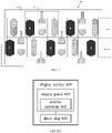
- the display device provided by some embodiments of the present disclosure further includes a drive chip, the drive chip is electrically connected to the display panel, and the drive chip is located on a side of the first sub-pixel in each repeating unit away from the second sub-pixel.
- an area of the orthographic projection of the first light-emitting voltage application electrode of the light-emitting element of the first sub-pixel on the base substrate is greater than an area of the orthographic projection of the first light-emitting voltage application electrode of the light-emitting element of the second sub-pixel on the base substrate.
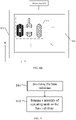
- Some embodiments of the present disclosure also provide a preparation method for preparing the display substrate according to any one of the embodiments of the present disclosure, and the preparation method includes: providing the base substrate; and forming the plurality of repeating units on the base substrate, in which each of the plurality of repeating units comprises the plurality of sub-pixels, each of the plurality of sub-pixels comprises the pixel circuit and the light-emitting element, the light-emitting element comprises the first light-emitting voltage application electrode, the second light-emitting voltage application electrode, and the light-emitting layer between the first light-emitting voltage application electrode and the second light-emitting voltage application electrode, the plurality of sub-pixels comprise the first sub-pixel and the second sub-pixel, the color of light emitted by the light-emitting element of the first sub-pixel is identical to the color of light emitted by the light-emitting element of the second sub-pixel, the shape of the first light-emitting voltage application electrode of the light-emitting element of the
- Some embodiments of the present disclosure also provide a display substrate, and the display substrate includes a base substrate and a plurality of repeating units on the base substrate, each of the plurality of repeating units comprises a plurality of sub-pixels, each of the plurality of sub-pixels comprises a light-emitting element and a pixel circuit for driving the light-emitting element to emit light, the pixel circuit comprises a drive circuit, and the light-emitting element comprises a first light-emitting voltage application electrode, a second light-emitting voltage application electrode, and a light-emitting layer between the first light-emitting voltage application electrode and the second light-emitting voltage application electrode; drive circuits of the plurality of sub-pixels are arranged in an array on the base substrate; the plurality of sub-pixels comprise a first sub-pixel and a second sub-pixel, and a color of light emitted by the light-emitting element of the first sub-pixel is identical to a color of light emitted by the light-
- a shape of the first drive electrode block is different from a shape of the auxiliary electrode block, the shape of the first drive electrode block is identical to a shape of the second drive electrode block, and an area of an orthographic projection of the first drive electrode block on the base substrate is identical to an area of an orthographic projection of the second drive electrode block on the base substrate.
- a shape of the first connection electrode block is identical to a shape of the second connection electrode block, and an area of an orthographic projection of the first connection electrode block on the base substrate is identical to an area of an orthographic projection of the second connection electrode block on the base substrate.
- the control terminal of the drive circuit of the pixel circuit of the first sub-pixel and the control terminal of the drive circuit of the pixel circuit of the second sub-pixel are arranged in a first direction, and in the first direction, the first drive electrode block is located on a side of the control terminal of the drive circuit of the pixel circuit of the first sub-pixel close to the control terminal of the drive circuit of the pixel circuit of the second sub-pixel.
- the first drive electrode block in the first direction, is located between the control terminal of the drive circuit of the pixel circuit of the first sub-pixel and the control terminal of the drive circuit of the pixel circuit of the second sub-pixel.
- the first connection electrode block is located on a side of the first drive electrode block away from the control terminal of the drive circuit of the pixel circuit of the second sub-pixel.
- the first connection electrode block is located between the control terminal of the drive circuit of the pixel circuit of the first sub-pixel and the control terminal of the drive circuit of the pixel circuit of the second sub-pixel.
- the first connection electrode block is located between the first drive electrode block and the auxiliary electrode block in the first direction.
- the second connection electrode block in the first direction, is located on a side of the control terminal of the drive circuit of the pixel circuit of the second sub-pixel away from the control terminal of the drive circuit of the pixel circuit of the first sub-pixel, and the second drive electrode block is located between the second connection electrode block and the first drive electrode block.
- a distance between a center of the control terminal of the drive circuit of the pixel circuit of the first sub-pixel and a center of the first drive electrode block is greater than a distance between a center of the control terminal of the drive circuit of the pixel circuit of the second sub-pixel and a center of the second drive electrode block.
- the display substrate includes a base substrate and a plurality of repeating units on the base substrate, each of the plurality of repeating units comprises a plurality of sub-pixels, each of the plurality of sub-pixels comprises a light-emitting element and a pixel circuit for driving the light-emitting element to emit light
- the light-emitting element comprises a first light-emitting voltage application electrode, a second light-emitting voltage application electrode, and a light-emitting layer between the first light-emitting voltage application electrode and the second light-emitting voltage application electrode
- the pixel circuit comprises a drive circuit, a second light-emitting control circuit, and a reset circuit
- the second light-emitting control circuit is electrically connected to a second light-emitting control signal line, a second terminal of the drive circuit, and the first light-emitting voltage application electrode of the light-emitting element, and is configured to, under control of a second light-emit
- the pixel circuit further comprises a data writing circuit
- the data writing circuit is electrically connected to a first terminal of the drive circuit and a first scanning signal line, and is configured to write a data signal to the control terminal of the drive circuit under control of a scanning signal provided by the first scanning signal line, in the first direction, the first scanning signal line is located between the second light-emitting control signal line and the first reset control signal line, the first light-emitting voltage application electrode of the light-emitting element of the first sub-pixel and the first light-emitting voltage application electrode of the light-emitting element of the second sub-pixel are arranged along the first direction, and in the first direction, the first scanning signal line connected to the data writing circuit of the pixel circuit of the second sub-pixel is located between the first light-emitting voltage application electrode of the light-emitting element of the first sub-pixel and the first light-emitting voltage application electrode of the light-emitting element of the second sub-pixel.
- the reset circuit is further electrically connected to a first reset power supply signal line, the reset circuit is configured to reset the control terminal of the drive circuit according to a first reset signal provided by the first reset power supply signal line under control of the first sub-reset control signal provided by the first reset control signal line, in the first direction, the first reset power supply signal line is located on a side of the first reset control signal line away from the second light-emitting control signal line, and the orthographic projection of the first light-emitting voltage application electrode of the light-emitting element of the first sub-pixel on the base substrate further at least partially overlaps with an orthographic projection of the first reset power supply signal line connected to the reset circuit of the pixel circuit of the second sub-pixel on the base substrate.
- all of the second light-emitting control signal line, the first reset control signal line, the first scanning signal line, and the first reset power supply signal line extend in a second direction, and the second direction is perpendicular to the first direction.
- the second light-emitting control signal line, the first reset control signal line, the first scanning signal line, and the first reset power supply signal line are parallel to each other.
- the first light-emitting voltage application electrode of the light-emitting element of the first sub-pixel comprises an auxiliary electrode block, a first drive electrode block, and a first connection electrode block
- the first drive electrode block, the auxiliary electrode block, and the first connection electrode block are electrically connected to each other and arranged in the first direction
- the first light-emitting voltage application electrode of the light-emitting element of the second sub-pixel comprises a second drive electrode block and a second connection electrode block
- the second drive electrode block and the second connection electrode block are electrically connected and arranged in the first direction, in the first direction
- the first connection electrode block and the auxiliary electrode block are both located on a side of the first drive electrode block away from the second drive electrode block
- the first connection electrode block is located between the auxiliary electrode block and the first drive electrode block
- the second connection electrode block is located on a side of the second drive electrode block away from the first drive electrode block
- a color of light emitted by the light-emitting element of the first sub-pixel is identical to a color of light emitted by the light-emitting element of the second sub-pixel, and a shape of the first light-emitting voltage application electrode of the light-emitting element of the first sub-pixel is different from a shape of the first light-emitting voltage application electrode of the light-emitting element of the second sub-pixel
- connection are not intended to define a physical connection or mechanical connection, but may comprise an electrical connection, directly or indirectly.
- "On,” “under,” “right,” “left” and the like are only used to indicate relative position relationship, and when the position of the object which is described is changed, the relative position relationship may be changed accordingly.
- FIG. 1 is a structural schematic diagram of a pixel repeating unit in a pixel arrangement structure, as shown in FIG. 1 , a pixel arrangement structure includes a plurality of pixel repeating units 400, and the plurality of pixel repeating units 400 are arranged in an array along a direction 405 and a direction 406.
- Each pixel repeating unit 400 includes a red sub-pixel 401, a blue sub-pixel 402, a first green sub-pixel 403, and a second green sub-pixel 404. As shown in FIG.
- the red sub-pixel 401 and the blue sub-pixel 402 are arranged in the direction 405, the first green sub-pixel 403 and the second green sub-pixel 404 are arranged in the direction 406, and in the direction 405, the first green sub-pixel 403 and the second green sub-pixel 404 are located between the red sub-pixel 401 and the blue sub-pixel 402.
- the brightness of the first green sub-pixel 403 and the brightness of the second green sub-pixel 404 are inconsistent, thereby resulting in a problem of missing detection of bright spots, i.e., some green sub-pixels cannot be detected.
- the brightness of the first green sub-pixel 403 is higher than that of the second green sub-pixel 404, thereby resulting in a phenomenon that the brightness of the first green sub-pixel 403 is relatively bright while the brightness of the second green sub-pixel 404 is relatively dark.
- each sub-pixel there is a parasitic capacitance between an anode of a light-emitting element and a gate electrode of a drive transistor, and the parasitic capacitance will affect a light-emitting brightness of the light-emitting element, and the larger the parasitic capacitance, the weaker the light-emitting brightness. The smaller the parasitic capacitance, the stronger the light-emitting brightness.
- a gate electrode of a drive transistor in a pixel circuit for driving the first green sub-pixel 403 is not blocked by an anode of a light-emitting element of the first green sub-pixel 403, while a gate electrode of a drive transistor in a pixel circuit for driving the second green sub-pixel 404 is blocked by an anode in a light-emitting element of the second green sub-pixel 404.
- At least some embodiment of the present disclosure provide a display substrate and a preparation method thereof, a display panel, and a display device.
- a light-emitting element of a first sub-pixel covers a gate electrode of a drive transistor of the first sub-pixel
- a light-emitting element of a second sub-pixel also covers a gate electrode of a drive transistor of the second sub-pixel, so as to reduce the difference between a parasitic capacitance between the light-emitting element of the first sub-pixel and a gate electrode of the drive transistor of the first sub-pixel and a parasitic capacitance between the light-emitting element of the second sub-pixel and a gate electrode of the drive transistor of the second sub-pixel, and make the pixel brightness of the first sub-pixel and the pixel brightness of the second sub-pixel reach the same, thereby improving the display uniformity and the display effect and solving the problem of the pixel brightness difference of the display panel.
- the display substrate has a simple structure, is easy to design and manufacture
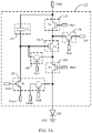
- FIG. 2 is a schematic block diagram of a display substrate provided by some embodiments of the present disclosure
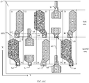
- FIG. 3A is a plane schematic diagram of a display substrate provided by some embodiments of the present disclosure
- FIG. 3A is a structural schematic diagram of a pixel circuit provided by some embodiments of the present disclosure
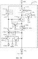
- FIG. 3B is a structural schematic diagram of a pixel circuit of a first sub-pixel provided by some embodiments of the present disclosure
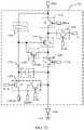
- FIG. 3C is a structural schematic diagram of a pixel circuit of a second sub-pixel provided by some embodiments of the present disclosure.
- the display substrate 100 provided by the embodiment of the present disclosure includes a base substrate 10 and a plurality of repeating units 11 on the base substrate 10, each repeating unit 11 includes a plurality of sub-pixels 12.
- Each sub-pixel 12 includes a light-emitting element 120 and a pixel circuit 121, the pixel circuit 121 is used for driving the light-emitting element 120 to emit light, and the pixel circuit 121 includes a drive circuit 122.
- the display substrate 100 may be applied to a display panel, such as an active matrix organic light-emitting diode (AMOLED) display panel or the like.
- the display substrate 100 may be an array substrate.
- the base substrate 10 may be a suitable substrate such as a glass substrate, a quartz substrate, and a plastic substrate, etc.
- the light-emitting element 120 of each sub-pixel 12 includes a first light-emitting voltage application electrode, a second light-emitting voltage application electrode, and a light-emitting layer between the first light-emitting voltage application electrode and the second light-emitting voltage application electrode.
- the plurality of sub-pixels 12 include a first sub-pixel G1 and a second sub-pixel G2.
- the pixel circuit 121 further includes a first light-emitting control circuit 123 and a second light-emitting control circuit 124.
- the drive circuit 122 includes a control terminal, a first terminal, and a second terminal, and is configured to provide a drive current for driving the light-emitting element 120 to emit light.
- the first light-emitting control circuit 123 is connected to the first terminal of the drive circuit 122 and a first voltage terminal VDD, and is configured to turn on or turn off a connection between the drive circuit 122 and the first voltage terminal VDD
- the second light-emitting control circuit 124 is electrically connected to the second terminal of the drive circuit 122 and the first light-emitting voltage application electrode of the light-emitting element 120, and is configured to turn on or turn off a connection between the drive circuit 122 and the light-emitting element 120.
- a pixel circuit 121a of the first sub-pixel G1 further includes a first parasitic circuit 125a
- a pixel circuit 121b of the second sub-pixel G2 further includes a second parasitic circuit 125b.
- the first parasitic circuit 125a is electrically connected to a control terminal of a drive circuit 122a of the pixel circuit 121a of the first sub-pixel G1 and a first light-emitting voltage application electrode of a light-emitting element 120a of the first sub-pixel G1, and is configured to control a voltage of the control terminal of the drive circuit 122a of the pixel circuit 121a of the first sub-pixel G1 based on a voltage of the first light-emitting voltage application electrode of the light-emitting element 120a of the first sub-pixel G1.
- the second parasitic circuit 125b is electrically connected to a control terminal of a drive circuit of a pixel circuit 121b of the second sub-pixel G2 and a first light-emitting voltage application electrode of a light-emitting element 120b of the second sub-pixel G2, and is configured to control a voltage of the control terminal of the drive circuit 122b of the pixel circuit 121b of the second sub-pixel G2 based on a voltage of the first light-emitting voltage application electrode of the light-emitting element 120b of the second sub-pixel G2.
- the pixel circuit 121 may further include a parasitic circuit, and the parasitic circuit is not shown in FIG. 3A , for example, a first parasitic circuit in the pixel circuit of the first sub-pixel G1 and a second parasitic circuit in the pixel circuit of the second sub-pixel G2 are not shown in FIG. 3A .
- the pixel circuit 121 further includes a data writing circuit 126, a storage circuit 127, a threshold compensation circuit 128, and a reset circuit 129.
- the data writing circuit 126 is electrically connected to the first terminal of the drive circuit 122 and is configured to write a data signal into the storage circuit 127 under control of a scanning signal;
- the storage circuit 127 is electrically connected to the control terminal of the drive circuit 122 and the first voltage terminal VDD, and is configured to store the data signal;
- the threshold compensation circuit 128 is electrically connected to the control terminal of the drive circuit 122 and the second terminal of the drive circuit 122, and is configured to perform threshold compensation on the drive circuit 122;
- the reset circuit 129 is electrically connected to the control terminal of the drive circuit 122 and the first light-emitting voltage application electrode of the light-emitting element 120, and is configured to reset the control terminal of the drive circuit 122 and the first light-emitting voltage application electrode of the light-emitting element 120 under control of a reset
- the drive circuit 122 includes a drive transistor T1
- the control terminal of the drive circuit 122 includes a gate electrode of the drive transistor T1
- the first terminal of the drive circuit 122 includes a first electrode of the drive transistor T1
- the second terminal of the drive circuit 122 includes a second electrode of the drive transistor T1.
- the data writing circuit 126 includes a data writing transistor T2
- the storage circuit 127 includes a third capacitor C2
- the threshold compensation circuit 128 includes a threshold compensation transistor T3
- the first light-emitting control circuit 123 includes a first light-emitting control transistor T4
- the second light-emitting control circuit 124 includes a second light-emitting control transistor T5
- the reset circuit 129 includes a first reset transistor T6 and a second reset transistor T7
- the reset control signal may include a first sub-reset control signal and a second sub-reset control signal.
- a first electrode of the data writing transistor T2 is electrically connected to the first electrode of the drive transistor T1, a second electrode of the data writing transistor T2 is configured to be electrically connected to a data line Vd to receive the data signal, and a gate electrode of the data writing transistor T2 is configured to be electrically connected to a first scanning signal line Ga1 to receive the scanning signal;
- a first electrode of the third capacitor C2 is electrically connected to the first voltage terminal VDD, and a second electrode of the third capacitor C2 is electrically connected to the gate electrode of the drive transistor T1;
- a first electrode of the threshold compensation transistor T3 is electrically connected to the second electrode of the drive transistor T1, a second electrode of the threshold compensation transistor T3 is electrically connected to the gate electrode of the drive transistor T1, and a gate electrode of the threshold compensation transistor T3 is configured to be electrically connected to a second scanning signal line Ga2 to receive a compensation control signal;
- a first electrode of the first reset transistor T6 is configured to be electrically connected to
- the first parasitic circuit 125a includes a first capacitor C11, and the first capacitor C11 includes a first electrode CC3a and a second electrode CC4a.
- the first electrode CC3a of the first capacitor C11 is electrically connected to the first light-emitting voltage application electrode of the light-emitting element 120a of the first sub-pixel G1
- the second electrode CC4a of the first capacitor C11 is electrically connected to the gate electrode of the drive transistor T1 of the pixel circuit 121a of the first sub-pixel G1.
- the second parasitic circuit 125b includes a second capacitor C12
- the second capacitor C12 includes a first electrode and a second electrode.
- the first electrode of the second capacitor C12 is electrically connected to the first light-emitting voltage application electrode of the light-emitting element 120b of the second sub-pixel G2
- the second electrode of the second capacitor C12 is electrically connected to the gate electrode of the drive transistor T1 of the pixel circuit 121b of the second sub-pixel G2.
- a capacitance value of the first capacitor C11 may be the same as a capacitance value of the second capacitor C12, so that a pixel brightness of the first sub-pixel G1 can be consistent with a pixel brightness of the second sub-pixel G2, and the display uniformity and the display effect can be improved.
- one of the first voltage terminal VDD and the second voltage terminal VSS is a high voltage terminal and the other of the first voltage terminal VDD and the second voltage terminal VSS is a low voltage terminal.
- the first voltage terminal VDD is a voltage source to output a constant first voltage, and the first voltage is a positive voltage
- the second voltage terminal VSS may be a voltage source to output a constant second voltage, the second voltage is a negative voltage or the like.
- the second voltage terminal VSS may be grounded.
- the pixel circuit 121a of the first sub-pixel G1 further includes a data writing circuit 126a, a storage circuit 127a, a threshold compensation circuit 128a, and a reset circuit 129a; and for the second sub-pixel G2, as shown in FIG. 3C , the pixel circuit 121b of the second sub-pixel G2 further includes a data writing circuit 126b, a storage circuit 127b, a threshold compensation circuit 128b, and a reset circuit 129b.
- connection relationship and function of each element in each circuit of the pixel circuit 121a of the first sub-pixel G1 and the pixel circuit 121b of the second sub-pixel G2 are similar to the example described above with respect to FIG. 3A , and the repetition is not repeated here again.
- the scanning signal may be the same as the compensation control signal, that is, the gate electrode of the data writing transistor T2 and the gate electrode of the threshold compensation transistor T3 may be electrically connected to a same signal line, such as the first scanning signal line Ga1, to receive the same signal (e.g., scanning signal), at this time, the display substrate 100 may not be provided with the second scanning signal line Ga2, thereby reducing the number of signal lines.
- the compensation control signal that is, the gate electrode of the data writing transistor T2 and the gate electrode of the threshold compensation transistor T3 may be electrically connected to a same signal line, such as the first scanning signal line Ga1, to receive the same signal (e.g., scanning signal), at this time, the display substrate 100 may not be provided with the second scanning signal line Ga2, thereby reducing the number of signal lines.
- the gate electrode of the data writing transistor T2 and the gate electrode of the threshold compensation transistor T3 may be electrically connected to different signal lines, i.e., the gate electrode of the data writing transistor T2 is electrically connected to the first scanning signal line Ga1, the gate electrode of the threshold compensation transistor T3 is electrically connected to the second scanning signal line Ga2, and a signal transmitted by the first scanning signal line Ga1 is identical to a signal transmitted by the second scanning signal line Ga2.
- the scanning signal and the compensation control signal may also be different, so that the gate electrode of the data writing transistor T2 and the threshold compensation transistor T3 can be separately and independently controlled, thereby increasing the flexibility of controlling the pixel circuit.
- the first light-emitting control signal may be identical to the second light-emitting control signal, that is, the gate electrode of the first light-emitting control transistor T4 and the gate electrode of the second light-emitting control transistor T5 may be electrically connected to a same signal line, such as the first light-emitting control signal line EM1, to receive the same signal (e.g., the first light-emitting control signal), and at this time, the display substrate 100 may not be provided with the second light-emitting control signal line EM2, thereby reducing the number of signal lines.
- the first light-emitting control signal may be identical to the second light-emitting control signal, that is, the gate electrode of the first light-emitting control transistor T4 and the gate electrode of the second light-emitting control transistor T5 may be electrically connected to a same signal line, such as the first light-emitting control signal line EM1, to receive the same signal (e.g., the first light-emitting control signal), and at this time,
- the gate electrode of the first light-emitting control transistor T4 and the gate electrode of the second light-emitting control transistor T5 may also be electrically connected to different signal lines, i.e., the gate electrode of the first light-emitting control transistor T4 is electrically connected to the first light-emitting control signal line EM1, the gate electrode of the second light-emitting control transistor T5 is electrically connected to the second light-emitting control signal line EM2, and a signal transmitted by the first light-emitting control signal line EM1 is identical to a signal transmitted by the second light-emitting control signal line EM2.
- first light-emitting control transistor T4 and the second light-emitting control transistor T5 are different types of transistors, for example, in a case where the first light-emitting control transistor T4 is a P-type transistor and the second light-emitting control transistor T5 is an N-type transistor, the first light-emitting control signal and the second light-emitting control signal may also be different, and the embodiment of the present disclosure is not limited to this case.
- the first sub-reset control signal may be identical to the second sub-reset control signal, that is, the gate electrode of the first reset transistor T6 and the gate electrode of the second reset transistor T7 may be electrically connected to a same signal line, such as the first reset control signal line Rst1, to receive the same signal (e.g., the first sub-reset control signal).
- the display substrate 100 may not be provided with the second reset control signal line Rst2, thereby reducing the number of signal lines.
- the gate electrode of the first reset transistor T6 and the gate electrode of the second reset transistor T7 may be electrically connected to different signal lines, i.e., the gate electrode of the first reset transistor T6 is electrically connected to the first reset control signal line Rst1, the gate electrode of the second reset transistor T7 is electrically connected to the second reset control signal line Rst2, and a signal transmitted by the first reset control signal line Rst1 is identical to a signal transmitted by the second reset control signal line Rst2.
- the first sub-reset control signal and the second sub-reset control signal may also be different.
- the second sub-reset control signal may be the same as the scanning signal, that is, the gate electrode of the second reset transistor T7 may be electrically connected to the first scanning signal line Ga1 to receive the scanning signal as the second sub-reset control signal.
- the first reset power supply terminal Vinit1 and the second reset power supply terminal Vinit2 may be DC reference voltage terminals to output constant DC reference voltages.
- the first reset power supply terminal Vinit1 and the second reset power supply terminal Vinit2 may be high voltage terminals or low voltage terminals, as long as the first reset power supply terminal Vinit1 and the second reset power supply terminal Vinit2 can provide the first reset signal and the second reset signal to reset the gate electrode of the drive transistor T1 and the first light-emitting voltage application electrode of the light-emitting element 120, and the present disclosure is not limited thereto.
- the drive circuit 122, the data writing circuit 126, the storage circuit 127, the threshold compensation circuit 128, and the reset circuit 129 in the pixel circuit as shown in FIGS. 3A-3B are only schematic.
- the specific structures of the drive circuit 122, the data writing circuit 126, the storage circuit 127, the threshold compensation circuit 128, and the reset circuit 129 can be set according to actual application requirements, and the embodiment of the present disclosure is not specifically limited to this case.
- transistors can be divided into N-type transistors and P-type transistors.
- the embodiments of the present disclosure elaborate the technical scheme of the present disclosure by taking a case that transistors are P-type transistors (e.g., P-type MOS transistors) as an example, that is, in the description of the present disclosure, the drive transistor T1, the data writing transistor T2, the threshold compensation transistor T3, the first light-emitting control transistor T4, the second light-emitting control transistor T5, the first reset transistor T6, the second reset transistor T7, etc. can be P-type transistors.
- P-type transistors e.g., P-type MOS transistors
- the transistors of the embodiments of the present disclosure are not limited to P-type transistors, and those skilled in the art can also use N-type transistors (e.g., N-type MOS transistors) to achieve the functions of one or more transistors in the embodiments of the present disclosure according to actual needs.
- N-type transistors e.g., N-type MOS transistors
- the transistors used in the embodiments of the present disclosure may be thin film transistors or field effect transistors or other switching devices with the same characteristics, and the thin film transistors may include oxide semiconductor thin film transistors, amorphous silicon thin film transistors, or polysilicon thin film transistors, etc.
- a source electrode and a drain electrode of a transistor can be symmetrical in structure, so the source electrode and the drain electrode of the transistor can be indistinguishable in physical structure.
- one of the two electrodes is directly described as a first electrode, and the other of the two electrodes is described as a second electrode, so the first electrodes and the second electrodes of all or part of the transistors in the embodiment of the present disclosure are interchangeable as required.
- connection relations, structures, and types, etc. of respective circuits e.g., the drive circuit 122a, the first light-emitting control circuit 123a, the second light-emitting control circuit 124a, the data writing circuit 126a, the storage circuit 127a, the threshold compensation circuit 128a, and the reset circuit 129a, etc.
- respective circuits e.g., the drive circuit 122a, the first light-emitting control circuit 123a, the second light-emitting control circuit 124a, the data writing circuit 126a, the storage circuit 127a, the threshold compensation circuit 128a, and the reset circuit 129a, etc.
- the drive circuit 122b the first light-emitting control circuit 123b, the second light-emitting control circuit 124b, the data writing circuit 126b, the storage circuit 127b, the threshold compensation circuit 128b, and the reset circuit 129b, etc.
- the structure and type of the drive circuit 122a in the pixel circuit 121a of the first sub-pixel G1 are the same as the structure and type of the drive circuit 122b in the pixel circuit 121b of the second sub-pixel G2.
- the respective circuits in the pixel circuit 121a of the first sub-pixel G1 and the corresponding respective circuits in the pixel circuit 121b of the second sub-pixel G2 can be prepared simultaneously using the same process, for example, the drive circuit 122a in the pixel circuit 121a of the first sub-pixel G1 and the drive circuit 122b in the pixel circuit 121b of the second sub-pixel G2 can be prepared simultaneously using the same patterning process.
- respective signal lines electrically connected to the respective circuits in the pixel circuit 121a of the first sub-pixel G1 is a first scanning signal line Ga1a, a second scanning signal line Ga2a, a first reset control signal line Rst1a, a second reset control signal line Rst2a, a first reset power supply terminal Vinitla, a second reset power supply terminal Vinit2a, a first light-emitting control signal line EM1a, a second light-emitting control signal line EM2a, and the data line Vd, respectively.
- respective signal lines electrically connected to the respective circuits in the pixel circuit 121b of the second sub-pixel G2 is a first scanning signal line Galb, a second scanning signal line Ga2b, a first reset control signal line Rstlb, a second reset control signal line Rst2b, a first reset power supply terminal Vinitlb, a second reset power supply terminal Vinit2b, a first light-emitting control signal line EM1b, a second light-emitting control signal line EM2b, and the data line Vd, respectively.
- the pixel circuit of the sub-pixel may also have a structure including other numbers of transistors, such as a 6T2C structure or a 9T2C structure, the embodiment of the present disclosure is not limited to this case.
- FIGS. 4A-4E are schematic diagrams of various layers of a pixel circuit provided by some embodiments of the present disclosure. The positional relationship of the respective circuits in the pixel circuit on a backplane will be described below with reference to FIGS. 4A-4E .
- Examples as shown in FIGS. 4A-4E takes the pixel circuit 121a of the first sub-pixel G1 as an example.
- the pixel circuit 121a of the first sub-pixel G1 includes the drive transistor T1, the data writing transistor T2, the threshold compensation transistor T3, the first light-emitting control transistor T4, the second light-emitting control transistor T5, the first reset transistor T6, and the second reset transistor T7, the first capacitor C11, and the third capacitor C2.
- 4A-4E also show the first scanning signal line Ga1a, the second scanning signal line Ga2a, the first reset control signal line Rst1a, the second reset control signal line Rst2a, a first reset power supply signal line Init1a of the first reset power supply terminal Vinitla, a second reset power supply signal line Init2a of the second reset power supply terminal Vinit2a, the first light-emitting control signal line EM1a, the second light-emitting control signal line EM2a, the data line Vd, a first power supply signal line VDD1 and a second power supply signal line VDD2 of the first voltage terminal VDD, which are connected to the pixel circuit 121a of the first sub-pixel G1, and the first power supply signal line VDD1 and the second power supply signal line VDD2 are electrically connected to each other.
- the first scanning signal line Ga1a and the second scanning signal line Ga2a are the same signal line
- the first reset power supply signal line Init1a and the second reset power supply signal line Init2a are the same signal line
- the first reset control signal line Rst1a and the second reset control signal line Rst2a are the same signal line
- the first light-emitting control signal line EM1a and the second light-emitting control signal line EM2a are the same signal line.
- FIG. 4A shows an active semiconductor layer 310 of the pixel circuit 121a.
- the active semiconductor layer 310 may be patterned using a semiconductor material.
- the active semiconductor layer 310 may be used to fabricate active layers of the above-mentioned drive transistor T1, the data writing transistor T2, the threshold compensation transistor T3, the first light-emitting control transistor T4, the second light-emitting control transistor T5, the first reset transistor T6, and the second reset transistor T7, and each of the active layers may include a source region, a drain region, and a channel region between the source region and the drain region.
- the active layers of the respective transistors are integrally provided.
- the active semiconductor layer 310 may be prepared by amorphous silicon, polysilicon, oxide semiconductor material, or the like. It should be noted that the above-mentioned source region and drain region may be regions doped with n-type impurities or p-type impurities.
- a gate electrode metal layer of the pixel circuit 121a may include a first conductive layer and a second conductive layer.
- a gate insulation layer (not shown) is formed on the active semiconductor layer 310 to protect the active semiconductor layer 310.
- FIG. 4B shows a first conductive layer 320 of the pixel circuit 121a, the first conductive layer 320 is disposed on the gate insulation layer so as to be insulated from the active semiconductor layer 310.
- the first conductive layer 320 may include a second electrode CC2a of the third capacitor C2, the first scanning signal line Ga1a, the second scanning signal line Ga2a, the first reset control signal line Rst1a, the second reset control signal line Rst2a, the first light-emitting control signal line EM1a, the second light-emitting control signal line EM2a, and gate electrodes of the drive transistor T1, the data writing transistor T2, the threshold compensation transistor T3, the first light-emitting control transistor T4, the second light-emitting control transistor T5, the first reset transistor T6, and the second reset transistor T7.
- the gate electrode of the data writing transistor T2 may be a portion where the first scanning signal line Ga1a overlaps the active semiconductor layer 310
- the gate electrode of the first light-emitting control transistor T4 may be a first portion where the first light-emitting control signal line EM1a/the second light-emitting control signal line EM2a overlaps the active semiconductor layer 310
- the gate electrode of the second light-emitting control transistor T5 may be a second portion where the first light-emitting control signal line EM1 a/the second light-emitting control signal line EM2a overlaps the active semiconductor layer 310
- the gate electrode of the first reset transistor T6 may be a first portion where the first reset control signal line RS1 a/the second reset control signal line Rst2a overlaps the active semiconductor layer 310
- the gate electrode of the second reset transistor T7 is a second portion where the first reset control signal line Rstla/the second reset control signal line Rst2a overlaps the active semiconductor
- respective dashed rectangular frames in FIG. 4A shows respective portions where the first conductive layer 320 overlaps the active semiconductor layer 310.
- the first scanning signal line Gala/the second scanning signal line Ga2a, the first reset control signal line Rst1 a/the second reset control signal line Rst2a, and the first light-emitting control signal line EM1a/the second light-emitting control signal line EM2a are arranged along a first direction X.
- the first scanning signal line Gala/the second scanning signal line Ga2a is located between the first reset control signal line Rst1a/the second reset control signal line Rst2a and the first light-emitting control signal line EM1a/second light-emitting control signal line EM2a.
- the second electrode CC4a of the first capacitor C11 (i.e., the second electrode CC2a of the third capacitor C2) is located between the first scanning signal line Gala/the second scanning signal line Ga2a and the first light-emitting control signal line EMI/the second light-emitting control signal line EM2a.
- the protrusion portion protruding from the second scanning signal line Ga2a is located on a side of the second scanning signal line Ga2a away from the first light-emitting control signal line EMIa/ the second light-emitting control signal line EM2a.
- the gate electrode of the data writing transistor T2, the gate electrode of the threshold compensation transistor T3, the gate electrode of the first reset transistor T6, and the gate electrode of the second reset transistor T7 are all located on a first side of the gate electrode of the drive transistor T1
- the gate electrode of the first light-emitting control transistor T4 and the gate electrode of the second light-emitting control transistor T5 are both located on a second side of the gate electrode of the drive transistor T1 and for example, in the example as shown in FIGS.
- the first side and the second side of the gate electrode of the drive transistor T1 of the pixel circuit 121a of the first sub-pixel G1 are opposite sides of the gate electrode of the drive transistor T1 in the first direction X.
- the first side of the gate electrode of the drive transistor T1 of the pixel circuit 121a of the first sub-pixel G1 may be an upper side of the gate electrode of the drive transistor T1
- the second side of the gate electrode of the drive transistor T1 of the pixel circuit 121a of the first sub-pixel G1 may be a lower side of the gate electrode of the drive transistor T1.
- the gate electrode of the data writing transistor T2 and the gate electrode of the first light-emitting control transistor T4 are both located on a third side of the gate electrode of the drive transistor T1, the first gate electrode of the threshold compensation transistor T3, the gate electrode of the second light-emitting control transistor T5, and the gate electrode of the second reset transistor T7 are all located on a fourth side of the gate electrode of the drive transistor T1, for example, in the example shown in FIGS.
- the third side and the fourth side of the gate electrode of the drive transistor T1 of the pixel circuit 121a of the first sub-pixel G1 are opposite sides of the gate electrode of the drive transistor T1 in the second direction Y, for example, as shown in FIGS.
- the third side of the gate electrode of the drive transistor T1 of the pixel circuit 121a of the first sub-pixel G1 may be a right side of the gate electrode of the drive transistor T1 of the pixel circuit 121a of the first sub-pixel G1
- the fourth side of the gate electrode of the drive transistor T1 of the pixel circuit 121a of the first sub-pixel G1 may be a left side of the gate electrode of the drive transistor T1 of the pixel circuit 121a of the first sub-pixel G1.
- FIG. 4C shows a second conductive layer 330 of the pixel circuit 120a.
- the second conductive layer 330 includes a first electrode CC1a of the third capacitor C2, the first reset power supply signal line Initla, the second reset power supply signal line Init2a, and the second power supply signal line VDD2.
- the second power supply signal line VDD2 is formed integrally with the first electrode CC1a of the third capacitor C2.
- the first electrode CC1a of the third capacitor C2 and the second electrode CC2a of the third capacitor C2 at least partially overlap to form the third capacitor C2.
- FIG. 4D shows a source-drain electrode metal layer 340 of the pixel circuit 121a, the source-drain electrode metal layer 340 includes the data line Vd and the first power supply signal line VDD1.
- FIG. 4E is a schematic diagram of a stacked positional relationship of the above-mentioned active semiconductor layer 310, the first conductive layer 320, the second conductive layer 330, and the source-drain electrode metal layer 340.
- the data line Vd is connected to the source region of the data writing transistor T2 in the active semiconductor layer 310 through at least one via hole (e.g., via hole 381a) in the gate insulation layer, the first insulation layer, and the second insulation layer.
- the first power supply signal line VDD1 is connected to the source region of the corresponding first light-emitting control transistor T4 in the active semiconductor layer 310 through at least one via hole (e.g., via hole 382a) in the gate insulation layer, the first insulation layer, and the second insulation layer.
- the first power supply signal line VDD1 is connected to the first electrode CC1a of the third capacitor C2 in the second conductive layer 330 through at least one via hole (e.g., via hole 3832a) in the second insulation layer.
- the first power supply signal line VDD1 is also connected to the second power supply signal line VDD2 in the second conductive layer 330 through at least one via hole (e.g., via hole 3831a) in the second insulation layer.
- the source-drain electrode metal layer 340 further includes a first connection portion 341a, a second connection portion 342a, and a third connection portion 343a.
- One terminal of the first connection portion 341a is connected to the drain region of the corresponding threshold compensation transistor T3 in the active semiconductor layer 310 through at least one via hole (e.g., via hole 384a) in the gate insulation layer, the first insulation layer, and the second insulation layer, and the other terminal of the first connection portion 341a is connected to the gate electrode of the drive transistor T1 (i.e., the second electrode CC2a of the third capacitor C2) in the first conductive layer 320 through at least one via hole (e.g., via hole 385a) in the first insulation layer and the second insulation layer.
- One terminal of the second connection portion 342a is connected to the first reset power supply signal line Initla/ the second reset power supply signal line Init2a through one via hole (e.g., via hole 386a) in the second insulation layer, and the other terminal of the second connection portion 342a is connected to the drain region of the second reset transistor T7 in the active semiconductor layer 310 through at least one via hole (e.g., via hole 387a) in the gate insulation layer, the first insulation layer, and the second insulation layer.
- the third connection portion 343a is connected to the drain region of the second light-emitting control transistor T5 in the active semiconductor layer 310 through at least one via hole (e.g., via hole 388a) in the gate insulation layer, the first insulation layer, and the second insulation layer.
- an intermediate layer (not shown) is formed on the above-mentioned source-drain electrode metal layer 340 to protect the source-drain electrode metal layer 340.
- the first light-emitting voltage application electrode of the light-emitting element of each sub-pixel may be on a side of the intermediate layer away from the base substrate.
- the first scanning signal line Ga1a, the second scanning signal line Ga2a, the first reset control signal line Rst1a, the second reset control signal line Rst2a, and the first reset p power supply signal line Initla, and the second reset power supply signal line Init2a are all located on the first side of the gate electrode of the drive transistor T1 of the pixel circuit 121a of the first sub-pixel G1, and the first light-emitting control signal line EM1a and the second light-emitting control signal line EM2a are both located on the second side of the drive transistor T1 of the pixel circuit 121a of the first sub-pixel G1.
- the first scanning signal line Ga1a, the second scanning signal line Ga2a, the first reset control signal line Rst1a, the second reset control signal line Rst2a, the first light-emitting control signal line EM1a, the second light-emitting control signal line EM2a, the first reset power supply signal line Initla, and the second reset power supply signal line Init2a all extend in the second direction Y, and the data line Vd extends in the first direction X.
- the first power supply signal line VDD1 extends in the first direction X and the second power supply signal line VDD2 extends in the second direction Y.
- the signal lines of the first voltage terminal VDD are gridded on the display substrate, that is, the first power supply signal line VDD1 and the second power supply signal line VDD2 are arranged in a grid pattern on the entire display substrate, so that a resistance of the signal lines of the first voltage terminal VDD is small and a voltage drop of the signal lines of the first voltage terminal VDD is low, and further the stability of the power supply voltage provided by the first voltage terminal VDD can be improved.
- the first scanning signal line Ga1a, the second scanning signal line Ga2a, the first reset control signal line Rst1a, the second reset control signal line Rst2a, the first light-emitting control signal line EM1a, and the second light-emitting control signal line EM2a are located on the same layer
- the first reset power supply signal line Init1a, the second reset power supply signal line Init2a, and the second power supply signal line VDD2 are located on the same layer.
- the first power supply signal line VDD1 and the data line Vd are located on the same layer.
- the positional arrangement relationship of the drive circuit, the first light-emitting control circuit, the second light-emitting control circuit, the data writing circuit, the storage circuit, the threshold compensation circuit, and the reset circuit, etc. in each pixel circuit is not limited to the examples as shown in FIGS. 4A-4E , and according to actual application requirements, positions of the drive circuit, the first light-emitting control circuit, the second light-emitting control circuit, the data writing circuit, the storage circuit, the threshold compensation circuit, and the reset circuit may be specifically set.
- FIG. 5A is a plane schematic diagram of a display substrate according to some embodiments of the present disclosure
- FIG. 5B is a plane schematic diagram of a repeating unit provided by some embodiments of the present disclosure
- FIG. 6A is a plane schematic diagram of another repeating unit provided by some embodiments of the present disclosure
- FIG. 6B is a layout diagram of a display substrate provided by some embodiments of the present disclosure
- FIG. 6C is a cross-sectional structural schematic diagram of a line L1-L1' in FIG. 6B
- FIG. 6D is a cross-sectional structural schematic diagram of a line L2-L2' in FIG. 6B
- FIG. 6E is a plane schematic diagram of another display substrate provided by some embodiments of the present disclosure.
- the pixel arrangement structure in the display substrate 10 may be a GGRB pixel arrangement structure to increase the PPI (pixel per inch) of the display panel including the display substrate 10, thereby increasing a visual resolution of the display panel under the same display resolution.
- each repeating unit 11 includes four sub-pixels, the four sub-pixels are the first sub-pixel G1, the second sub-pixel G2, a third sub-pixel R, and a fourth sub-pixel B, respectively, and the four sub-pixels can adopt GGRB arrangement. It should be noted that only two complete repeating units 11 are shown in FIG. 5A , but the present disclosure is not limited thereto.
- the display substrate 10 includes a plurality of repeating units 11, and the plurality of repeating units 11 are arranged in an array along the first direction X and the second direction Y.
- regions 31 to 40 may be regions where pixel circuits of respective sub-pixels on the base substrate 10 are located, for example, regions 31 to 35 are located in a first row and regions 36 to 40 are located in a second row; regions 31 and 36 are in a first column, regions 32 and 37 are in a second column, regions 33 and 38 are in a third column, regions 34 and 39 are in a fourth column, and regions 35 and 40 are in a fifth column.
- regions 31 to 40 may be regions where pixel circuits of respective sub-pixels on the base substrate 10 are located, for example, regions 31 to 35 are located in a first row and regions 36 to 40 are located in a second row; regions 31 and 36 are in a first column, regions 32 and 37 are in a second column, regions 33 and 38 are in a third column, regions 34 and 39 are in a fourth column, and regions 35 and 40 are in a fifth column.
- regions 31 to 40 are in a fifth column.
- the pixel circuit of the first sub-pixel G1 is located in the region 32
- the pixel circuit of the second sub-pixel G2 is located in the region 37
- the pixel circuit of the third sub-pixel R is located in the region 38
- the pixel circuit of the fourth sub-pixel B is located in the region 36.
- row may represent a row corresponding to areas where respective pixel circuits are located
- column may represent a column corresponding to areas where respective pixel circuits are located.
- the light-emitting element 120 is configured to receive a light-emitting signal (e.g., may be a current signal) during operation and emit light of an intensity corresponding to the light-emitting signal.
- the light-emitting element 120 may be a light-emitting diode, and the light-emitting diode may be, for example, an organic light-emitting diode (OLED), a quantum dot light-emitting diode (QLED), or the like, but embodiments of the present disclosure are not limited thereto.
- OLED organic light-emitting diode
- QLED quantum dot light-emitting diode
- the light-emitting element 120 includes a first light-emitting voltage application electrode 1201, a second light-emitting voltage application electrode 1202, and a light-emitting layer 1203 between the first light-emitting voltage application electrode 1201 and the second light-emitting voltage application electrode 1202.
- a first light-emitting voltage application electrode 1201 a second light-emitting voltage application electrode 1202
- a light-emitting layer 1203 between the first light-emitting voltage application electrode 1201 and the second light-emitting voltage application electrode 1202.
- the light-emitting element of the first sub-pixel G1 includes a first light-emitting voltage application electrode 1201a, the second light-emitting voltage application electrode 1202, and a light-emitting layer 1203a
- the light-emitting element of the second sub-pixel G2 includes a first light-emitting voltage application electrode 1201b, the second light-emitting voltage application electrode 1202, and a light-emitting layer 1203a.
- an orthographic projection of the first light-emitting voltage application electrode 1201a of the light-emitting element of the first sub-pixel G1 on the base substrate 10 at least partially overlaps with an orthographic projection of a control terminal 1221a of the drive circuit of the pixel circuit of the first sub-pixel G1 on the base substrate 10
- an orthographic projection of the first light-emitting voltage application electrode 1201b of the light-emitting element of the second sub-pixel G2 on the base substrate 10 at least partially overlaps with an orthographic projection of a control terminal 1221b of the drive circuit of the pixel circuit of the second sub-pixel G2 on the base substrate 10.
- the first light-emitting voltage application electrode 1201a of the light-emitting element of the first sub-pixel G1 and the first light-emitting voltage application electrode 1201b of the light-emitting element of the second sub-pixel G2 may be located on the same layer, and the second light-emitting voltage application electrode 1202 of the light-emitting element of the first sub-pixel G1 and the second light-emitting voltage application electrode 1202 of the light-emitting element of the second sub-pixel G2 may be integrally provided.
- an orthographic projection of the light-emitting layer 1203a of the light-emitting element of the first sub-pixel G1 on the base substrate 10 is continuous with an orthographic projection of the light-emitting layer 1203a of the light-emitting element of the second sub-pixel G2 on the base substrate 10, that is, the light-emitting layer 1203a of the light-emitting element of the first sub-pixel G1 and the light-emitting layer 1203a of the light-emitting element of the second sub-pixel G2 can be prepared by an opening hole in a high-precision metal mask (FMM) plate, which can effectively reduce the process difficulty of FMM
- FMM high-precision metal mask
- the light-emitting layer 1203a of the light-emitting element of the first sub-pixel G1 and the light-emitting layer 1203a of the light-emitting element of the second sub-pixel G2 are integrated.
- materials of the light-emitting layers 1203 of respective sub-pixels may be selected according to different colors of light emitted by the light-emitting elements 120 of respective sub-pixels.
- a material of the light-emitting layer 1203 of each sub-pixel includes a fluorescent light-emitting material, a phosphorescent light-emitting material, or the like.
- the first light-emitting voltage application electrode 1201 is an anode
- the second light-emitting voltage application electrode 1202 is a cathode
- both the first light-emitting voltage application electrode 1201 and the second light-emitting voltage application electrode 1202 are prepared by conductive materials.
- a first organic layer is disposed between the first light-emitting voltage application electrode 1201 and the light-emitting layer 1203, and a second organic layer is disposed between the second light-emitting voltage application electrode 1202 and the light-emitting layer 1203.
- the first organic layer and the second organic layer are used for planarization and may be omitted.
- a color of light emitted by the light-emitting element 120a of the first sub-pixel G1 is the same as a color of light emitted by the light-emitting element 120b of the second sub-pixel G2, that is, the first sub-pixel G1 and the second sub-pixel G2 are sub-pixels of the same color.
- the first sub-pixel G1 and the second sub-pixel G2 are sensitive color sub-pixels.
- the display substrate 100 adopts a red green blue (RGB) display mode
- the above sensitive color is green, that is, the first sub-pixel G1 and the second sub-pixel G2 are both green sub-pixels.
- the third sub-pixel R may be a red sub-pixel and the fourth sub-pixel B may be a blue sub-pixel.
- each repeating unit 11 may form two virtual pixels, and the third sub-pixel R and the fourth sub-pixel B in the repeating unit 11 are respectively shared by the two virtual pixels.
- the sub-pixels in the plurality of repeating units 11 form a pixel array. In a row direction of the pixel array, the density of sub-pixels is 1.5 times the density of virtual pixels, and in a column direction of the pixel array, the density of sub-pixels is 1.5 times the density of virtual pixels.
- the first sub-pixel G1 and the second sub-pixel G2 belong to two virtual pixels respectively.
- the division of virtual pixels is related to the driving mode, and the specific division mode of virtual pixels can be determined according to the actual driving mode, which is not specifically limited by the present disclosure.
- the orthographic projection of the control terminal 1221a of the drive circuit of the pixel circuit of the first sub-pixel G1 on the base substrate 10 is located within the orthographic projection of the first light-emitting voltage application electrode 1201a of the light-emitting element 120a of the first sub-pixel G1 on the base substrate 10.
- the orthographic projection of the control terminal 1221b of the drive circuit of the pixel circuit of the second sub-pixel G2 on the base substrate 10 is located within the orthographic projection of the first light-emitting voltage application electrode 1201b of the light-emitting element 120b of the second sub-pixel G2 on the base substrate 10.
- the orthographic projection of the first light-emitting voltage application electrode 1201a of the light-emitting element 120a of the first sub-pixel G1 on the base substrate 10 completely covers the orthographic projection of the control terminal 1221a of the drive circuit of the pixel circuit of the first sub-pixel G1 on the base substrate 10
- the orthographic projection of the first light-emitting voltage application electrode 1201b of the light-emitting element 120b of the second sub-pixel G2 on the base substrate 10 completely covers the orthographic projection of the control terminal 1221b of the drive circuit of the pixel circuit of the second sub-pixel G2 on the base substrate 10
- an area of the orthographic projection of the first light-emitting voltage application electrode 1201a of the light-emitting element 120a of the first sub-pixel G1 on the base substrate 10 may be larger than an area of the orthographic projection of the control terminal 1221a of the drive circuit of the pixel circuit of the first sub-pixel G1 on the base substrate 10, and an area of the orthographic projection of the first light-
- the drive circuit 122a of the pixel circuit of the first sub-pixel G1 includes the drive transistor T1
- the control terminal 1221a of the drive circuit 122a of the pixel circuit of the first sub-pixel G1 is the gate electrode of the drive transistor T1 of the pixel circuit of the first sub-pixel G1
- the orthographic projection of the first light-emitting voltage application electrode of the light-emitting element 120a of the first sub-pixel G1 on the base substrate 10 at least partially overlaps with an orthographic projection of the gate electrode of the drive transistor T1 of the first sub-pixel G1 on the base substrate 10; and as shown in FIG.
- the drive circuit 122b of the pixel circuit of the second sub-pixel G2 includes the drive transistor T1
- the control terminal 1221b of the drive circuit 122b of the pixel circuit of the second sub-pixel G2 is the gate electrode of the drive transistor T1 of the pixel circuit of the second sub-pixel G2
- the orthographic projection of the first light-emitting voltage application electrode of the light-emitting element 120b of the second sub-pixel G2 on the base substrate 10 at least partially overlaps with an orthographic projection of the gate electrode of the drive transistor T1 of the second sub-pixel G2 on the base substrate 10.
- the orthographic projection of the gate electrode of the drive transistor T1 of the first sub-pixel G1 on the base substrate 10 is located within the orthographic projection of the first light-emitting voltage application electrode of the light-emitting element 120a of the first sub-pixel G1 on the base substrate 10; and the orthographic projection of the gate electrode of the drive transistor T1 of the second sub-pixel G2 on the base substrate 10 is located within the orthographic projection of the first light-emitting voltage application electrode of the light-emitting element 120b of the second sub-pixel G2 on the base substrate 10.
- an area of an overlapping portion between the orthographic projection of the control terminal 1221a of the drive circuit of the pixel circuit of the first sub-pixel G1 on the base substrate 10 and the orthographic projection of the first light-emitting voltage application electrode 1201a of the light-emitting element of the first sub-pixel G1 on the base substrate 10 is a first area A1.
- An area of an overlapping portion between the orthographic projection of the control terminal 1221b of the drive circuit of the pixel circuit of the second sub-pixel G2 on the base substrate 10 and the orthographic projection of the first light-emitting voltage application electrode 1201b of the light-emitting element of the second sub-pixel G2 on the base substrate 10 is a second area A2, and a ratio of the first area A1 to the second area A2 satisfies a following relation: Amin ⁇ A 1 /A 2 ⁇ Amax , where A1 represents the first area, A2 represents the second area, Amin represents a minimum ratio threshold and is 90%, and Amax represents a maximum ratio threshold and is 110%.
- the first area A1 may be greater than or equal to the second area A2, in this case, the minimum ratio threshold Amin may be 90%, and the maximum ratio threshold Amax may also be 100%; and in other examples, the first area A1 may be smaller than the second area A2, in this case, the minimum ratio threshold Amin may be 95% and the maximum ratio threshold Amax may be 105%.
- the embodiment of the present disclosure is not specifically limited to specific values of the minimum ratio threshold and the maximum ratio threshold, as long as the difference between the first area A1 and the second area A2 is ensured to be small (e.g., less than 10%), and furthermore, the difference between the parasitic capacitance between the first light-emitting voltage application electrode 1201a of the light-emitting element of the first sub-pixel G1 and the control terminal 1221a of the drive circuit of the first sub-pixel G1 (i.e., the first capacitor C11 as shown in FIG.
- the parasitic capacitance between the first light-emitting voltage application electrode 1201b of the light-emitting element of the second sub-pixel G2 and the control terminal 1221b of the drive circuit of the second sub-pixel G2 i.e., the second capacitor C12 as shown in FIG. 3C
- the second capacitor C12 as shown in FIG. 3C
- the ratio of the first area A1 and the second area A2 is between the above-mentioned minimum ratio threshold and the maximum ratio threshold, even in a low gray scale (e.g., 64 gray scales), that is, in a case where the human eye recognition capability is high, the user may not be able to see the brightness difference between the first sub-pixel G1 and the second sub-pixel G2, thereby effectively improving the display effect of the display panel and enhancing the user experience.
- a low gray scale e.g. 64 gray scales
- a shape of the first light-emitting voltage application electrode 1201a of the light-emitting element 120a of the first sub-pixel G1 is different from a shape of the first light-emitting voltage application electrode 1201b of the light-emitting element of the second sub-pixel G2.
- the shape of the first light-emitting voltage application electrode 1201a of the light-emitting element of the first sub-pixel G1 may be an octagon
- the shape of the first light-emitting voltage application electrode 1201b of the light-emitting element of the second sub-pixel G2 may be pentagonal.
- the area of the orthographic projection of the first light-emitting voltage application electrode 1201a of the light-emitting element of the first sub-pixel G1 on the base substrate 10 is different from the area of the orthographic projection of the first light-emitting voltage application electrode 1201b of the light-emitting element of the second sub-pixel G2 on the base substrate 10
- the area of the orthographic projection of the first light-emitting voltage application electrode 1201a of the light-emitting element of the first sub-pixel G1 on the base substrate 10 is larger than the area of the orthographic projection of the first light-emitting voltage application electrode 1201b of the light-emitting element of the second sub-pixel G2 on the base substrate 10.
- the first light-emitting voltage application electrode 1201a of the light-emitting element 120a of the first sub-pixel G1 includes an auxiliary electrode block Ae, an orthographic projection of the auxiliary electrode block Ae on the base substrate 10 at least partially overlaps with the orthographic projection of the control terminal 1221a of the drive circuit of the pixel circuit of the first sub-pixel G1 on the base substrate 10.
- the orthographic projection of the control terminal 1221a of the drive circuit of the pixel circuit of the first sub-pixel G1 on the base substrate 10 is located within the orthographic projection of the auxiliary electrode block Ae on the base substrate 10.
- the orthographic projection of the gate electrode of the drive transistor T1 of the first sub-pixel G1 on the base substrate 10 is located within the orthographic projection of the auxiliary electrode block Ae of the first light-emitting voltage application electrode of the light-emitting element 120a of the first sub-pixel G1 on the base substrate 10.
- the auxiliary electrode block Ae severs as the first electrode CC3 of the first capacitor C11, the control terminal 1221a of the drive circuit 122a of the first sub-pixel G1 is multiplexed as the second electrode CC4 of the first capacitor C11, that is, the auxiliary electrode block Ae is the first electrode CC3 of the first capacitor C11, and the control terminal 1221a of the drive circuit 122a of the first sub-pixel G1 (i.e., the gate electrode of the drive transistor T1 of the first sub-pixel G1) is the second electrode CC4 of the first capacitor C11.
- a shape of the auxiliary electrode block Ae may be rectangular, and a shape of the orthographic projection of the auxiliary electrode block Ae on the base substrate 10 is the same as the shape of the auxiliary electrode block Ae, that is, rectangular.
- the present disclosure is not limited thereto, and the shape of the auxiliary electrode block Ae may be pentagonal, hexagonal, elliptical, or the like.
- the first light-emitting voltage application electrode 1201a of the light-emitting element 120a of the first sub-pixel G1 further includes a first drive electrode block De1, and the first drive electrode block De1 is electrically connected to the auxiliary electrode block Ae.
- a shape of the first drive electrode block De1 may be a pentagon, and a shape of the orthographic projection of the first drive electrode block De1 on the base substrate 10 is identical to the shape of the first drive electrode block De1, that is, a pentagon.
- Pentagon may consist of a triangle and a rectangle.
- the first drive electrode block De1 and the auxiliary electrode block Ae are integrally provided, and thus, the shape of the first light-emitting voltage application electrode 1201a may be an octagon, and the octagon may consist of a pentagon and a rectangle.
- first drive electrode block De1 and the auxiliary electrode block Ae may be separately provided, as long as the first drive electrode block De1 and the auxiliary electrode block Ae can be electrically connected to each other.
- the first drive electrode block De1 and the auxiliary electrode block Ae may be simultaneously formed by the same patterning process.
- the first drive electrode block De1 and the auxiliary electrode block Ae are located on the same layer.
- the orthographic projection of the first drive electrode block De1 on the base substrate 10 the orthographic projection of the light-emitting layer 1203a of the light-emitting element of the first sub-pixel G1 on the base substrate 10 at least partially overlap.
- second light-emitting voltage application electrodes of light-emitting elements of all sub-pixels on the display substrate are provided integrally, that is, the second light-emitting voltage application electrode 1202 covers the entire base substrate 10, that is, the second light-emitting voltage application electrode 1202 may be a plane-shaped electrode.
- the second light-emitting voltage application electrode 1202 may be a plane-shaped electrode.
- a portion where the plane-shaped second light-emitting voltage application electrode 1202 overlaps with the first light-emitting voltage application electrode 1201a of the light-emitting element of the first sub-pixel G1 may be represented as the second light-emitting voltage application electrode 1202 of the light-emitting element of the first sub-pixel G1
- a portion where the plane-shaped second light-emitting voltage application electrode overlaps with the first light-emitting voltage application electrode 1201b of the light-emitting element of the second sub-pixel G2 may be represented as the second light-emitting voltage application electrode 1202 of the light-emitting element of the second sub-pixel G2.
- the second light-emitting voltage application electrode 1202 of the light-emitting element of the first sub-pixel G1 and the second light-emitting voltage application electrode 1202 of the light-emitting element of the second sub-pixel G2 are integrally provided.
- the light-emitting layer of the light-emitting element of the first sub-pixel G1 and the light-emitting layer of the light-emitting element of the second sub-pixel G2 are integrally provided.
- a portion where the light-emitting layer 1203a overlaps with the first light-emitting voltage application electrode 1201a of the light-emitting element of the first sub-pixel G1 may be represented as the light-emitting layer of the light-emitting element of the first sub-pixel G1
- a portion where the light-emitting layer 1203a overlaps with the first light-emitting voltage application electrode 1201b of the light-emitting element of the second sub-pixel G2 may be represented as the light-emitting layer of the light-emitting element of the second sub-pixel G2.
- the display substrate 100 further includes a pixel definition layer 160
- the pixel definition layer 160 is located on a side of the first light-emitting voltage application electrode of the light-emitting element of each sub-pixel away from the base substrate 10 and includes a first opening, the first opening exposes the first light-emitting voltage application electrode 1201a of the light-emitting element of the first sub-pixel G1 and the first light-emitting voltage application electrode 1201b of the light-emitting element of the second sub-pixel G2, at least part of the light-emitting layer 1203a of the light-emitting element of the first sub-pixel G1 and at least part of the light-emitting layer 1203a of the light-emitting element of the second sub-pixel G2 are located in the first opening and cover an exposed portion of the first light-emitting voltage application electrode 1201a and an exposed portion of the first light-emitting voltage application electrode 1201b, a part area where the first opening overlaps with
- the light-emitting layer of each light-emitting element may include an electroluminescent layer itself and other common layers located on both sides of the electroluminescent layer, for example, other common layers comprise a hole injection layer, a hole transport layer, an electron injection layer, an electron transport layer, and the like, but in the drawings of the present disclosure, only the electroluminescent layer in the light-emitting layer is shown, and other common layers are not shown.
- the orthographic projection of the first drive electrode block De1 on the base substrate 10 may not completely overlap with the orthographic projection of the second light-emitting voltage application electrode 1202 of the light-emitting element of the first sub-pixel G1 on the base substrate 10, for example, the orthographic projection of the first drive electrode block De1 on the base substrate 10 is located within the orthographic projection of the second light-emitting voltage application electrode 1202 of the light-emitting element of the first sub-pixel G1 on the base substrate 10, and the orthographic projection of the light-emitting layer 1203a of the light-emitting element of the first sub-pixel G1 on the base substrate 10 may also be located within the orthographic projection of the second light-emitting voltage application electrode 1202 of the light-emitting element of the first sub-pixel G1 on the base substrate 10.
- the orthographic projection of the first drive electrode block De1 on the base substrate 10 the orthographic projection of the light-emitting layer 1203a of the light-emitting element of the first sub-pixel G1 on the base substrate 10 overlap, for the first sub-pixel G1, a portion of the light-emitting layer of the light-emitting element of the first sub-pixel G1 corresponding to the first opening of the pixel definition layer 160 is used for emitting light.
- the first light-emitting voltage application electrode 1201b of the light-emitting element 120b of the second sub-pixel G2 includes a second drive electrode block De2.
- An orthographic projection of the second drive electrode block De2 on the base substrate 10 at least partially overlaps with the orthographic projection of the control terminal 1221b of the drive circuit of the pixel circuit of the second sub-pixel G2 on the base substrate 10.
- the orthographic projection of the control terminal 1221b of the drive circuit of the pixel circuit of the second sub-pixel G2 on the base substrate 10 may be located within the orthographic projection of the second drive electrode block De2 on the base substrate 10.
- the orthographic projection of the gate electrode of the drive transistor T1 of the second sub-pixel G2 on the base substrate 10 is located within the orthographic projection of the second drive electrode block De2 of the first light-emitting voltage application electrode of the light-emitting element 120b of the second sub-pixel G2 on the base substrate 10.
- the second drive electrode block De2 may be multiplexed as the first electrode of the second capacitor C12
- the control terminal 1221b of the drive circuit 122b of the second sub-pixel G2 may be multiplexed as the second electrode of the second capacitor C12
- the second drive electrode block De2 is the first electrode of the second capacitor C12
- the control terminal 1221b of the drive circuit 122b of the second sub-pixel G2 i.e., the gate electrode of the drive transistor T1 of the second sub-pixel G2 is the second electrode of the second capacitor C12.
- the shape of the first drive electrode block De1 may be identical to a shape of the second drive electrode block De2, that is, the shape of the second drive electrode block De2 may also be a pentagon.
- a shape of the orthographic projection of the second drive electrode block De2 on the base substrate 10 is identical to the shape of the second drive electrode block De2, that is, a pentagon.
- the area of the orthographic projection of the first drive electrode block De1 on the base substrate 10 is identical to an area of the orthographic projection of the second drive electrode block De2 on the base substrate 10.
- the shape of the first drive electrode block De1 and the shape of the second drive electrode block De2 may be rectangles, rhombuses, or the like.
- the shape of the first drive electrode block De1 and the shape of the second drive electrode block De2 may be different, and the present disclosure is not limited thereto.
- the orthographic projection of the second drive electrode block De2 on the base substrate 10 the orthographic projection of the light-emitting layer 1203a of the light-emitting element of the second sub-pixel G2 on the base substrate 10
- the orthographic projection of the second light-emitting voltage application electrode 1202 of the light-emitting element of the second sub-pixel G2 on the base substrate 10 all at least partially overlap.
- the orthographic projection of the second drive electrode block De2 on the base substrate 10 may not completely overlap with the orthographic projection of the second light-emitting voltage application electrode 1202 of the light-emitting element of the second sub-pixel G2 on the base substrate 10, for example, the orthographic projection of the second drive electrode block De2 on the base substrate 10 is located within the orthographic projection of the second light-emitting voltage application electrode 1202 of the light-emitting element of the second sub-pixel G2 on the base substrate 10.
- the orthographic projection of the second drive electrode block De2 on the base substrate 10 the orthographic projection of the light-emitting layer 1203a of the light-emitting element of the second sub-pixel G2 on the base substrate 10 overlap, for the second sub-pixel G2, a portion of the light-emitting layer of the light-emitting element of the second sub-pixel G2 corresponding to the first opening of the pixel definition layer 160 is used for emitting light.
- the first sub-pixel G1 and the second sub-pixel G2 are arranged along the first direction X, and the first direction X is parallel to a surface of the base substrate 10.
- the auxiliary electrode block Ae is located on a side of the first drive electrode block De1 away from the light-emitting element of the second sub-pixel G2, that is, as shown in FIG. 5B , in the first direction X, the first drive electrode block De1 is located between the auxiliary electrode block Ae and the second drive electrode block De2.
- the orthographic projection of the auxiliary electrode block Ae on the base substrate 10 does not overlap with the orthographic projection of the light-emitting layer 1203a of the light-emitting element of the first sub-pixel G1 on the base substrate 10.
- the orthographic projection of the auxiliary electrode block Ae on the base substrate 10 does not completely overlap with the orthographic projection of the light-emitting layer 1203a of the light-emitting element of the first sub-pixel G1 on the base substrate 10.
- the first light-emitting voltage application electrode of the light-emitting element of the first sub-pixel G1 further includes a first connection electrode block Ce1, in the first direction X, the first connection electrode block Ce1 is located on a side of the first drive electrode block De1 away from the light-emitting element of the second sub-pixel G2, the first connection electrode block Ce1 is located between the auxiliary electrode block Ae and the first drive electrode block De1, and is electrically connected to both the auxiliary electrode block Ae and the first drive electrode block De1.
- the first connection electrode block Ce1, the auxiliary electrode block Ae, and the first drive electrode block De1 are all provided integrally. It should be noted that in other examples, the first connection electrode block Ce1, the auxiliary electrode block Ae, and the first drive electrode block De1 may be separately provided, as long as the first connection electrode block Ce1, the auxiliary electrode block Ae, and the first drive electrode block De1 can be electrically connected to each other.
- the first connection electrode block Ce1 is used to connect the first drive electrode block De1 and the pixel circuit of the first sub-pixel G1.
- the first connection electrode block Ce1, the auxiliary electrode block Ae, and the first drive electrode block De1 are located on the same layer.
- the first connection electrode block Ce1, the auxiliary electrode block Ae, and the first drive electrode block De1 may be simultaneously formed by the same patterning process.
- a shape of the first connection electrode block Ce1 may be a regular shape, for example, a rectangle, a diamond, or the like; and the shape of the first connection electrode block Ce1 also may be an irregular shape.
- the shape of the auxiliary electrode block Ae and the shape of the first connection electrode block Ce1 are both rectangles, and in the second direction Y, a width of the auxiliary electrode block Ae is smaller than a width of the first connection electrode block Ce1, i.e., the auxiliary electrode block Ae and the first connection electrode block Ce1 form a stepped shape. In the second direction Y, the width of the first connection electrode block Ce1 is smaller than a maximum width of the first drive electrode block De1.
- the first drive electrode block De1 has five internal angles, and the five internal angles may include two right angles, two obtuse angles, and an acute angle, and the first connection electrode block Ce1 extends from a side, where the acute angle of the first drive electrode block De1 is located, in a direction of the first drive electrode block De1 away from the light-emitting element of the second sub-pixel G2.
- the orthographic projection of the first connection electrode block Ce1 on the base substrate 10 does not overlap with the orthographic projection of the light-emitting layer 1203a of the light-emitting element of the first sub-pixel G1 on the base substrate 10, and the orthographic projection of the first connection electrode block Ce1 on the base substrate 10 does not overlap with the orthographic projection of the control terminal 1221a of the drive circuit of the pixel circuit of the first sub-pixel G1 on the base substrate 10.
- the orthographic projection of the first connection electrode block Ce1 on the base substrate 10 may partially overlap with the orthographic projection of the control terminal 1221a of the drive circuit of the pixel circuit of the first sub-pixel G1 on the base substrate 10.
- an area of an overlapping portion between the orthographic projection of the first connection electrode block Ce1 on the base substrate 10 and the orthographic projection of the control terminal 1221a of the drive circuit of the pixel circuit of the first sub-pixel G1 on the base substrate 10 is smaller than an area of an overlapping portion between the orthographic projection of the auxiliary electrode block Ae on the base substrate 10 and the orthographic projection of the control terminal 1221a of the drive circuit of the pixel circuit of the first sub-pixel G1 on the base substrate 10.
- the display substrate 100 further includes an intermediate layer 101.
- the pixel circuit 121 of each sub-pixel is located between the intermediate layer 101 and the base substrate 10
- the light-emitting element 120 is located on a side of the intermediate layer 101 away from the base substrate 10, that is, the intermediate layer 101 is located between the light-emitting element 120 and the base substrate 10.
- layers where light-emitting elements of all sub-pixels are located constitute a first functional layer group
- layers where pixel circuits of all sub-pixels are located constitute a second functional layer group, that is, in a direction perpendicular to the surface of the base substrate 10
- the first functional layer group is located on the side of the intermediate layer 101 away from the base substrate 10
- the second functional layer group is located on a side of the intermediate layer 101 close to the base substrate 10 that is, the second functional layer group is located between the intermediate layer 101 and the base substrate 10
- the intermediate layer 101 is located between the first functional layer group and the second functional layer group.
- the intermediate layer 101 is located between the first functional layer group and the second functional layer group.
- the drive circuit 122, the data writing circuit 126, the storage circuit 127, the threshold compensation circuit 128, and the reset circuit 129 as shown in FIG. 3A are all located in the second functional layer group.
- the first parasitic circuit 125a in the pixel circuit 121a of the first sub-pixel G1 and the second parasitic circuit 125b in the pixel circuit 121b of the second sub-pixel G2 are also located in the second functional layer group.
- the first functional layer group may include a plurality of sub-layers, for example, the first functional layer group may include a sub-layer where the first light-emitting voltage application electrode 1201a of the light-emitting element of the first sub-pixel G1 is located, a sub-layer where the second light-emitting voltage application electrode 1202 of the light-emitting element of the first sub-pixel G1 is located, and a sub-layer where the light-emitting layer 1203a of the light-emitting element of the first sub-pixel G1 is located.
- the second functional layer group may also include a plurality of sub-layers.
- the second functional layer group may include sub-layers where respective elements in the pixel circuit of the first sub-pixel G2 are located.
- the second functional layer group may include a sub-layer where the gate electrode of the transistor is located, a sub-layer where the source electrode and the drain electrode of the transistor are located, a sub-layer where the active layer is located, and a sub-layer where the gate insulation layer is located, etc.
- the intermediate layer 101 may be a flat layer.
- the first light-emitting voltage application electrode 1201a of the light-emitting element of the first sub-pixel G1 is on a side of the light-emitting layer 1203a of the light-emitting element of the first sub-pixel G1 close to the intermediate layer 101
- the second light-emitting voltage application electrode 1202 of the light-emitting element of the first sub-pixel G1 is on a side of the light-emitting layer 1203a of the light-emitting element of the first sub-pixel G1 away from the intermediate layer 101.
- the intermediate layer 101 includes a first via hole h1
- the first connection electrode block Ce1 extends to the first via hole h1 and is electrically connected to the pixel circuit of the first sub-pixel G1 through the first via hole h1, for example, the first connection electrode block Ce1 is electrically connected to the second light-emitting control circuit 124a of the pixel circuit of the first sub-pixel G1 through the first via hole h1.
- the first connection electrode block Ce1 may cover and fill the first via hole h1.
- the first connection electrode block Ce1 is electrically connected to the second electrode of the second light-emitting control transistor T5 of the pixel circuit of the first sub-pixel G1 through the first via hole h1.
- the pixel circuit 121 may include the active semiconductor layer 310, the gate electrode metal layer (including the first conductive layer 320 and the second conductive layer 330), and the source-drain electrode metal layer 340.
- the active semiconductor layer 310 is located between the base substrate 10 and the gate electrode metal layer
- the gate electrode metal layer is located between the active semiconductor layer 310 and the source-drain electrode metal layer 340.
- the first conductive layer 320 of the gate electrode metal layer is located between the active semiconductor layer 310 and the second conductive layer 330 of the gate electrode metal layer, and the second conductive layer 330 of the gate electrode metal layer is located between the first conductive layer 320 of the gate electrode metal layer and the source-drain electrode metal layer 340.
- active layers of respective transistors e.g., the drive transistor T1, the data writing transistor T2, the threshold compensation transistor T3, the first light-emitting control transistor T4, the second light-emitting control transistor T5, the first reset transistor T6, and the second reset transistor T7, etc.
- active layers of respective transistors in the pixel circuit 121 of each sub-pixel are located in the active semiconductor layer 310
- gate electrodes of respective transistors in the pixel circuit 121 are located in the first conductive layer 320 of the gate electrode metal layer
- source electrodes and drain electrodes of respective transistors in the pixel circuit 121 are located in the source-drain electrode metal layer 340.
- the first connection electrode block Ce1 extends to the source-drain electrode metal layer of the pixel circuit through the first via hole h1.
- the first light-emitting voltage application electrode of the light-emitting element of the second sub-pixel G2 further includes a second connection electrode block Ce2, and the second connection electrode block Ce2 is electrically connected to the second drive electrode block De2.
- the second connection electrode block Ce2 is integrally provided with the second drive electrode block De2. It should be noted that in other examples, the second connection electrode block Ce2 and the second drive electrode block De2 may be separately provided, as long as the second connection electrode block Ce2 and the second drive electrode block De2 can be electrically connected to each other.
- the second connection electrode block Ce2 is used to connect the second drive electrode block De2 and the pixel circuit of the second sub-pixel G2.
- the second connection electrode block Ce2 is located on a side of the second drive electrode block De2 away from the light-emitting element of the first sub-pixel G1, that is, as shown in FIGS. 6A and 6B , the second drive electrode block De2 is located between the second connection electrode block Ce2 and the first drive electrode block De1 in the first direction X.
- the second connection electrode block Ce2 and the second drive electrode block De2 are located on the same layer.
- the second connection electrode block Ce2 and the second drive electrode block De2 may be formed simultaneously by the same patterning process.
- a shape of the second connection electrode block Ce2 may be a regular shape, for example, a rectangle, and a diamond, etc.
- the shape of the second connection electrode block Ce2 may be an irregular shape.
- a width of the second connection electrode block Ce2 is smaller than a maximum width of the second drive electrode block De2.
- the second drive electrode block De2 includes five internal angles, the five internal angles may include two right angles, two obtuse angles, and an acute angle, and the second connection electrode block Ce2 extends from a side, where the acute angle of the second drive electrode block De2 is located, in a direction of the second drive electrode block De2 away from the light-emitting element of the first sub-pixel G1.
- the shape of the first connection electrode block Ce1 may be identical to the shape of the second connection electrode block Ce2.
- the orthographic projection of the second connection electrode block Ce2 on the base substrate 10 does not overlap with the orthographic projection of the light-emitting layer 1203a of the light-emitting element of the second sub-pixel G2 on the base substrate 10, and the orthographic projection of the second connection electrode block Ce2 on the base substrate 10 does not overlap with the orthographic projection of the control terminal 1221b of the drive circuit of the pixel circuit of the second sub-pixel G2 on the base substrate 10.
- the present disclosure is not limited to this case, and the orthographic projection of the second connection electrode block Ce2 on the base substrate 10 may partially overlap with the orthographic projection of the control terminal 1221b of the drive circuit of the pixel circuit of the second sub-pixel G2 on the base substrate 10.
- an area of an overlapping portion between the orthographic projection of the second connection electrode block Ce2 on the base substrate 10 and the orthographic projection of the control terminal 1221b of the drive circuit of the pixel circuit of the second sub-pixel G2 on the base substrate 10 is smaller than an area of an overlapping portion between the orthographic projection of the second drive electrode block De2 on the base substrate 10 and the orthographic projection of the control terminal 1221b of the drive circuit of the pixel circuit of the second sub-pixel G2 on the base substrate 10.
- the first light-emitting voltage application electrode 1201b of the light-emitting element of the second sub-pixel G2 is on a side of the light-emitting layer 1203a of the light-emitting element of the second sub-pixel G2 close to the intermediate layer 101
- the second light-emitting voltage application electrode 1202 of the light-emitting element of the second sub-pixel G2 is on a side of the light-emitting layer 1203a of the light-emitting element of the second sub-pixel G2 away from the intermediate layer 101.
- the intermediate layer 101 includes a second via hole h2, and the second connection electrode block Ce2 extends to the second via hole h2 and is electrically connected to the pixel circuit of the second sub-pixel G2 through the second via hole h2, for example, the second connection electrode block Ce2 is electrically connected to the second light-emitting control circuit 124b of the pixel circuit of the second sub-pixel G2 through the second via hole h2.
- the second connection electrode block Ce2 may cover and fill the second via hole h2.
- the second connection electrode block Ce2 is electrically connected to the second electrode of the second light-emitting control transistor T5 of the pixel circuit 121b of the second sub-pixel G2 through the second via hole h2.
- the second connection electrode block Ce2 extends to the source-drain electrode metal layer of the pixel circuit through the second via hole h2.
- the third sub-pixel R and the fourth sub-pixel B are arranged along the second direction Y, and in the second direction Y, the first sub-pixel G1 and the second sub-pixel G2 are located between the third sub-pixel R and the fourth sub-pixel B, the second direction Y is parallel to the surface of the base substrate 10, and the first direction X and the second direction Y are perpendicular to each other.
- a line connecting a center of the first sub-pixel G1 and a center of the second sub-pixel G2 is a first center line
- a line connecting a center of the third sub-pixel R and a center of the fourth sub-pixel B is a second center line.
- a length of the first center line is shorter than a length of the second center line.
- the first center line and the second center line are vertically bisected with each other, and the first center line is substantially parallel to the first direction X and the second center line is substantially parallel to the second direction Y.
- the light-emitting element of the third sub-pixel R includes a first light-emitting voltage application electrode, a second light-emitting voltage application electrode, and a light-emitting layer.
- the light-emitting element of the fourth sub-pixel B includes a first light-emitting voltage application electrode 1201d, a second light-emitting voltage application electrode 1202d, and a light-emitting layer 1203d.
- the third sub-pixel R a portion, where the plane-shaped second light-emitting voltage application electrode 1202 overlaps with the first light-emitting voltage application electrode of the light-emitting element of the third sub-pixel R, may be represented as the second light-emitting voltage application electrode of the light-emitting element of the third sub-pixel R; and for the fourth sub-pixel B, a portion, where the plane-shaped second light-emitting voltage application electrode overlaps with the first light-emitting voltage application electrode of the light-emitting element of the fourth sub-pixel B, may be represented as the second light-emitting voltage application electrode of the light-emitting element of the fourth sub-pixel B.
- the second light-emitting voltage application electrode of the light-emitting element of the first sub-pixel G1 the second light-emitting voltage application electrode of the light-emitting element of the second sub-pixel G2, the second light-emitting voltage application electrode of the light-emitting element of the third sub-pixel R, and the second light-emitting voltage application electrode of the light-emitting element of the fourth sub-pixel B are integrated.
- the orthographic projection of the first light-emitting voltage application electrode of the light-emitting element of the third sub-pixel R on the base substrate 10 may at least partially overlap with the orthographic projection of the control terminal of the drive circuit of the pixel circuit of the third sub-pixel R on the base substrate 10.
- the orthographic projection of the first light-emitting voltage application electrode 1201d of the light-emitting element of the fourth sub-pixel B on the base substrate 10 may also at least partially overlap with the orthographic projection of the control terminal of the drive circuit of the pixel circuit of the fourth sub-pixel B on the base substrate 10.
- the orthographic projection of the control terminal 1221d of the drive circuit of the pixel circuit of the fourth sub-pixel B on the base substrate 10 is located within the orthographic projection of the first light-emitting voltage application electrode 1201d of the light-emitting element of the fourth sub-pixel B on the base substrate 10.
- the first light-emitting voltage application electrode of the light-emitting element of the third sub-pixel R includes a third drive electrode block De3 and a third connection electrode block Ce3, and the third drive electrode block De3 and the third connection electrode block Ce3 are electrically connected to each other
- the first light-emitting voltage application electrode 1201d of the light-emitting element of the fourth sub-pixel B includes a fourth drive electrode block De4 and a fourth connection electrode block Ce4, and the fourth drive electrode block De4 and the fourth connection electrode block Ce4 are electrically connected to each other.
- the orthographic projection of the control terminal 1221c of the drive circuit of the pixel circuit of the third sub-pixel R on the base substrate 10 at least partially overlaps with the orthographic projection of the third drive electrode block De3 on the base substrate 10; and as shown in FIG. 6D , the orthographic projection of the control terminal 1221d of the drive circuit of the pixel circuit of the fourth sub-pixel B on the base substrate 10 at least partially overlaps with the orthographic projection of the fourth drive electrode block De4 on the base substrate 10, for example, the orthographic projection of the control terminal 1221d of the drive circuit of the pixel circuit of the fourth sub-pixel B on the base substrate 10 is located within the orthographic projection of the fourth drive electrode block De4 on the base substrate 10.
- the third connection electrode block Ce3 is used to connect the third drive electrode block De3 and the pixel circuit of the third sub-pixel R; and the fourth connection electrode block Ce4 is used to connect the fourth drive electrode block De4 and the pixel circuit of the fourth sub-pixel B.
- the pixel circuit of the third sub-pixel R further includes a third parasitic circuit
- the pixel circuit of the fourth sub-pixel B further includes a fourth parasitic circuit.
- the third parasitic circuit includes a fourth capacitor
- the fourth parasitic circuit includes a fifth capacitor.
- the third drive electrode block De3 is multiplexed as a first electrode of the fourth capacitor
- the control terminal of the drive circuit of the third sub-pixel R is multiplexed as a second electrode of the fourth capacitor
- the fourth drive electrode block De4 is multiplexed as a first electrode of the fifth capacitor
- the control terminal of the drive circuit of the fourth sub-pixel B is multiplexed as a second electrode of the fifth capacitor.
- a shape of the third drive electrode block De3 may be a regular hexagon, and a shape of the fourth drive electrode block De4 may also be a regular hexagon.
- the shape of the third connection electrode block Ce3 may also be an irregular hexagon, and the shape of the fourth connection electrode block Ce4 may also be an irregular hexagon.
- the shape of the third drive electrode block De3 and the shape of the fourth drive electrode block De4 may be rectangles, long ellipses, etc.
- the present disclosure does not specifically limit the shape of the third drive electrode block De3, the shape of the third connection electrode block Ce3, the shape of the fourth drive electrode block De4, and the shape of the fourth connection electrode block Ce4.
- the third connection electrode block Ce3 may be a portion protruding outward from one side (e.g., a lower right side of the hexagon) of the hexagonal third drive electrode block De3; and the fourth connection electrode block Ce4 may be a portion protruding outward from one side (e.g., a lower left side of the hexagonal) of the hexagonal fourth drive electrode block De4.
- the area of the drive electrode block of each sub-pixel can be specifically set according to the luminous efficiency of a luminescent material. For example, if the luminous efficiency of the luminescent material is higher, the area of the drive electrode block of the sub-pixel can be smaller; and while the luminous efficiency of the luminescent material is lower, the area of the drive electrode block of the sub-pixel can be larger.
- an area of the third drive electrode block De3 is smaller than an area of the fourth drive electrode block De4.
- the area of the third drive electrode block De3 is larger than an area of the first drive electrode block De1, and the area of the third drive electrode block De3 is larger than an area of the second drive electrode block De2.
- the third drive electrode block De3 and the third connection electrode block Ce3 are integrally provided, and the fourth drive electrode block De4 and the fourth connection electrode block Ce4 are also integrally provided.
- the third drive electrode block De3 and the third connection electrode block Ce3 may be separately provided, as long as the third drive electrode block De3 and the third connection electrode block Ce3 can be electrically connected to each other.
- the fourth drive electrode block De4 and the fourth connection electrode block Ce4 may be separately provided, as long as the fourth drive electrode block De4 and the fourth connection electrode block Ce4 can be electrically connected to each other.
- the third drive electrode block De3 and the third connection electrode block Ce3 are located on the same layer.
- the fourth drive electrode block De4 and the fourth connection electrode block Ce4 are located on the same layer.
- the first light-emitting voltage application electrode of the light-emitting element of the third sub-pixel R is on a side of the light-emitting layer of the light-emitting element of the third sub-pixel R close to the intermediate layer 101
- the second light-emitting voltage application electrode of the light-emitting element of the third sub-pixel R is on a side of the light-emitting layer of the light-emitting element of the third sub-pixel R away from the intermediate layer 101;
- the first light-emitting voltage application electrode 1201d of the light-emitting element of the fourth sub-pixel B is on a side of the light-emitting layer 1203d of the light-emitting element of the fourth sub-pixel B close to the intermediate layer 101
- the second light-emitting voltage application electrode 1202d of the light-emitting element of the fourth sub-pixel B is on a side of the light-emitting layer 1203d of the light-emitting element of the fourth sub-pixel B away from the intermediate layer 101.
- the intermediate layer 101 includes a third via hole h3, and the third connection electrode block Ce3 extends to the third via hole h3 and is electrically connected to the pixel circuit of the third sub-pixel R through the third via hole h3.
- the third connection electrode block Ce3 may cover and fill the third via hole h3.
- the intermediate layer 101 includes a fourth via hole h4, and the fourth connection electrode block Ce4 extends to the fourth via hole h4 and is electrically connected to the pixel circuit of the fourth sub-pixel B through the fourth via hole h4.
- the fourth connection electrode block Ce4 may cover and fill the fourth via hole h4.
- connection electrode block Ce3 extends to the source-drain electrode metal layer of the pixel circuit through the third via hole h3; and the fourth connection electrode block Ce4 extends to the source-drain electrode metal layer of the pixel circuit through the fourth via hole h4.
- the third connection electrode block Ce3 extends to the source-drain electrode metal layer of the pixel circuit through the third via hole h3, so as to be electrically connected to the second electrode of the second light-emitting control transistor of the third sub-pixel R located on the source-drain electrode metal layer of the pixel circuit.
- the fourth connection electrode block Ce4 extends to the source-drain electrode metal layer of the pixel circuit through the fourth via hole h4, so as to be electrically connected to the second electrode of the second light-emitting control transistor of the fourth sub-pixel B located on the source-drain electrode metal layer of the pixel circuit.
- the third connection electrode block Ce3 is located on a side of the third drive electrode block De3 away from the auxiliary electrode block Ae of the first sub-pixel G1 in the first direction X, and the third connection electrode block Ce3 is located on a side of the third drive electrode block De3 close to the fourth drive electrode block De4 in the second direction Y, that is, in the example as shown in FIGS. 6A and 6B , the third connection electrode block Ce3 is located on the lower right side of the third drive electrode block De3, that is, the shape of the first light-emitting voltage application electrode 1201c of the light-emitting element of the third sub-pixel R may be a Q-shaped mirror symmetric shape.
- the fourth connection electrode block Ce4 is located on a side of the fourth drive electrode block De4 away from the auxiliary electrode block Ae of the first sub-pixel G1 in the first direction X, and the fourth connection electrode block Ce4 is located on a side of the fourth drive electrode block De4 close to the third drive electrode block De3 in the second direction Y, that is, in the example as shown in FIGS. 6A and 6B , the fourth connection electrode block Ce4 is located on the lower left side of the fourth drive electrode block De4, that is, a shape of the first light-emitting voltage application electrode 1201d of the light-emitting element of the fourth sub-pixel B may be a Q-shape.
- the third connection electrode block Ce3 is electrically connected to the second light-emitting control circuit 124c of the pixel circuit of the third sub-pixel R through the third via hole h3, and for example, the third connection electrode block Ce3 is electrically connected to the second electrode of the second light-emitting control transistor of the pixel circuit of the third sub-pixel R through the third via hole h3.
- the fourth connection electrode block Ce4 is electrically connected to the second light-emitting control circuit 124d of the pixel circuit of the fourth sub-pixel B through the fourth via hole h4, for example, the fourth connection electrode block Ce4 is electrically connected to the second electrode of the second light-emitting control transistor of the pixel circuit of the fourth sub-pixel B through the fourth via hole h4.
- an intermediate layer (not shown) is formed on the source-drain electrode metal layer 340 as shown in FIG. 6D , and the first light-emitting voltage application electrode of the light-emitting element of each sub-pixel is provided on the intermediate layer.
- the first connection electrode block Ce1, the first drive electrode block De1 and the auxiliary electrode block Ae of the first light-emitting voltage application electrode of the light-emitting element of the first sub-pixel G1, the second connection electrode block Ce2 and the second drive electrode block De2 of the first light-emitting voltage application electrode of the light-emitting element of the second sub-pixel G2, the third connection electrode block Ce3 and the third drive electrode block De3 of the first light-emitting voltage application electrode of the light-emitting element of the third sub-pixel R, and the fourth connection electrode block Ce4 and the fourth drive electrode block De4 of the first light-emitting voltage application electrode of the light-emitting element of the fourth sub-pixel B are all disposed on the intermediate layer, the first connection electrode block Ce1 of the first sub-pixel G1 is connected to the second light-emitting control transistor T5 in the pixel circuit 121a of the first sub-pixel G1 through the first via hole h1, the second connection electrode block Ce2 of the second sub-pixel G2 is connected
- the orthographic projection of the auxiliary electrode block Ae of the first sub-pixel G1 on the base substrate at least partially overlaps with the orthographic projection of the gate electrode of the drive transistor in the pixel circuit 121a of the first sub-pixel G1 on the base substrate
- the orthographic projection of the second drive electrode block De2 of the second sub-pixel G2 on the base substrate at least partially overlaps with the orthographic projection of the gate electrode of the drive transistor in the pixel circuit 121b of the second sub-pixel G2 on the base substrate
- the orthographic projection of the third drive electrode block De3 of the third sub-pixel R on the base substrate at least partially overlaps with the orthographic projection of the gate electrode of the drive transistor in the pixel circuit of the third sub-pixel R on the base substrate
- the orthographic projection of the fourth drive electrode block De4 of the fourth sub-pixel B on the base substrate at least partially overlaps with the orthographic projection of the gate electrode of the drive transistor in the pixel circuit of the fourth sub-pixel B on the base substrate.
- FIG. 6E shows drive electrode blocks of respective sub-pixels, auxiliary electrode blocks of respective first sub-pixels, and connection electrode blocks of respective sub-pixels
- FIG. 6E also shows via holes corresponding to respective connection electrode blocks.
- the connection electrode block of each sub-pixel may cover and fill the corresponding via hole.
- the first connection electrode block covers and fills the first via hole h1
- the second connection electrode block covers and fills the second via hole h2
- the third connection electrode block covers and fills the third via hole h3
- the fourth connection electrode block covers and fills the fourth via hole h4.
- the respective via holes are located above the corresponding connection electrode blocks in FIG. 6E .
- respective via holes are arranged as a plurality of rows of via holes, and respective via holes in each row are arranged in an order of the third via hole h3, the first via hole h1, the fourth via hole h4, and the second via hole h2, i.e., the third via hole h3, the first via hole h1, the fourth via hole h4, and the second via hole h2 are one arrangement period HT1, in the arrangement period HT1, the first via hole h1 corresponds to the first sub-pixel G1 located in the second row and adjacent to the first via hole h1, the second via hole h2 corresponds to the second sub-pixel G2 located in the first row and adjacent to the second via hole h2, the third via hole h3 corresponds to the third sub-pixel R located in the first row and adjacent to the third via hole h3, and the fourth via hole h4 corresponds to the fourth sub-pixel B located in the first row and adjacent to the fourth via hole h4.
- respective via holes in each row are located on the same straight line, that is, the first via hole h1, the third via hole h3, the second via hole h2, and the fourth via hole h4 in each arrangement period HT1 are located on the same straight line, and the arrangement periods HT1 are also located on the same straight line.
- a distance between any two adjacent via holes is a first fixed distance d1, that is, as shown in FIG. 6E , in the arrangement period HT1, a distance between the first via hole h1 and the fourth via hole h4 is the first fixed distance d1, a distance between the first via hole h1 and the third via hole h3 is also the first fixed distance d1, a distance between the second via hole h2 and the third via hole h3 is also the first fixed distance d1, and a distance between the second via hole h2 and the fourth via hole h4 is also the first fixed distance d1.
- "two adjacent via holes” means that there is no via hole between the two adjacent via holes, and the first fixed distance d1 can represent the distance between centers of the two adjacent via holes in the second direction Y.
- respective first via holes h1 and respective second via holes h2 are arranged as a plurality of first via hole columns
- respective third via holes h3 and respective fourth via holes h4 are arranged as a plurality of second via hole columns
- the first via hole columns and the second via hole columns are alternately arranged, that is, the plurality of first via hole columns may be odd-numbered columns and the plurality of second via hole columns may be even-numbered columns.
- respective first via holes h1 and respective second via holes h2 are located on the same straight line
- respective third via holes h3 and respective fourth via holes h4 are also located on the same straight line.
- a distance between any adjacent first via hole h1 and second via hole h2 is a second fixed distance d2
- a distance between any adjacent third via hole h3 and fourth via hole h4 is a third fixed distance d3
- the second fixed distance d2 and the third fixed distance d3 are equal.
- the second fixed distance d2 may represent a distance between a center of the first via hole h1 and a center of the second via hole h2 that is adj acent to the first via hole h1 in the first direction X
- the third fixed distance d3 may represent a distance between a center of the third via hole h3 and a center of the fourth via hole h4 that is adjacent to the third via hole h3 in the first direction X.
- the plurality of repeating units 11 are arranged along the second direction Y to form a plurality of repeating unit groups, and the plurality of repeating unit groups are arranged along the first direction X.
- the first connection electrode block, the second connection electrode block, the third connection electrode block, and the fourth connection electrode block are located between two adjacent repeating unit groups, and in the first direction X, at least a portion of the auxiliary electrode block is located on a side of the auxiliary electrode block away from the first drive electrode block and between two adjacent repeating units in the repeating unit group adjacent to the repeating unit group in which the auxiliary electrode block is located.
- a P-th repeating unit group is located on a first row and a (P+1)-th repeating unit group is located on a second row.
- at least a portion of the auxiliary electrode block Ae is located on a side of the auxiliary electrode block Ae away from the first drive electrode block De1 and between two adjacent repeating units in the repeating unit group (i.e., the P-th repeating unit group) adjacent to the repeating unit group (i.e., the (P+1)-th repeating unit group) in which the auxiliary electrode block Ae is located, for example, as shown in FIG.
- At least a portion of the auxiliary electrode block Ae in the repeating unit located in the second row extends to the first row and is located between two adjacent repeating units located in the first row, for example, at least a portion of the auxiliary electrode block Ae in the repeating unit located in the second row is located between the adjacent third sub-pixel R and the fourth sub-pixel B in the first row.
- the second light-emitting control transistor of the second light-emitting control circuit 124a of the first sub-pixel G1 includes a second electrode 1241a (e.g., drain electrode) and an active layer 1242a.
- the drive transistor of the drive circuit of the first sub-pixel G1 includes a gate electrode 1221a (i.e., the control terminal of the drive circuit 122a) and an active layer 1222a. It should be noted that FIG. 6C does not show the gate electrode and the first electrode of the second light-emitting control transistor of the first sub-pixel G1, and the first electrode and the second electrode of the drive transistor of the first sub-pixel G1, etc.
- a gate insulation layer is between the active semiconductor layer 310 and the first conductive layer 320, that is, as shown in FIG. 6C , a gate insulation layer 131 is between the gate electrode 1221a of the drive transistor of the first sub-pixel G1 and the active layer 1222a of the drive transistor of the first sub-pixel G1, and the gate insulation layer 131 covers the entire display substrate 100, whereby the gate insulation layer 131 is also between the gate electrode and the active layer of the second light-emitting control transistor.
- the gate electrode 1221a of the drive transistor of the first sub-pixel G1 is on a side of the gate insulation layer 131 away from the base substrate 10. As shown in FIG.
- the first light-emitting control signal line EM1a connected to the first light-emitting control circuit of the first sub-pixel G1 and the second light-emitting control signal line EM2a connected to the second light-emitting control circuit of the first sub-pixel G1 are also disposed on a side of the gate insulation layer 131 away from the base substrate 10.
- the orthographic projection of the first connection electrode block Ce1 on the base substrate 10 at least partially overlaps with the orthographic projection of the second light-emitting control signal line EM2a (i.e., the first light-emitting control signal line EM1a connected to the first light-emitting control circuit of the first sub-pixel G1) connected to the second light-emitting control circuit of the pixel circuit of the first sub-pixel G1 on the base substrate 10.
- the orthographic projection of the first connection electrode block Ce1 on the base substrate 10 at least partially overlaps with the orthographic projection of the second light-emitting control signal line EM2a (i.e., the first light-emitting control signal line EM1a connected to the first light-emitting control circuit of the first sub-pixel G1) connected to the second light-emitting control circuit of the pixel circuit of the first sub-pixel G1 on the base substrate 10.
- a first insulation layer 132 is further provided on the gate electrode 1221a of the drive transistor of the first sub-pixel G1, and a first electrode CC1a of the third capacitor C2 of the first sub-pixel G1 is provided on a side of the first insulation layer 132 away from the base substrate 10.
- a second insulation layer 133 is provided on a side of the second electrode CC2a of the third capacitor C2 away from the base substrate 10.
- the second electrode 1241a of the second light-emitting control transistor of the first sub-pixel G1 is on a side of the second insulation layer 133 away from the base substrate 10, and is electrically connected to the active layer 1242a of the second light-emitting control transistor through a via hole 388a penetrating the second insulation layer 133, the first insulation layer 132, and the gate insulation layer 131.
- the first insulation layer 132 and the second insulation layer 133 also cover the entire display substrate 100.
- a first connection portion 341a of the first sub-pixel G1 is also provided on a side of the second insulation layer 133 away from the base substrate 10.
- the first connection portion 341a of the first sub-pixel G1 is electrically connected to the gate electrode 1221a of the drive transistor of the first sub-pixel G1 through the via hole 385a penetrating the second insulation layer 133, the first electrode CC1a of the third capacitor C2 the first sub-pixel G1, and the first insulation layer 132.
- the orthographic projection of the first connection portion 341a on the base substrate 10 at least partially overlaps with the orthographic projection of the gate electrode 1221a of the drive transistor of the first sub-pixel G1 on the base substrate 10, that is, the orthographic projection of the first connection portion 341a on the base substrate 10, the orthographic projection of the gate electrode 1221a of the drive transistor of the first sub-pixel G1 on the base substrate 10, and the orthographic projection of the auxiliary electrode block Ae on the base substrate 10 at least partially overlap.
- metal layers such as the first electrode CC1a of the third capacitor C2 of the first sub-pixel G1, the first connection portion 341a of the first sub-pixel G1, and the like, are further provided between the first electrode CC3a (i.e., the auxiliary electrode block Ae) and the second electrode CC4a (i.e., the gate electrode 1221a of the drive transistor of the first sub-pixel G1) of the first capacitor C11.
- auxiliary electrode block Ae and the first connection portion 341a of the first sub-pixel G1 there may also be a parasitic capacitance between the auxiliary electrode block Ae and the first electrode CC1a of the third capacitor C2 of the first sub-pixel G1
- gate electrode 1221a of the drive transistor of the first sub-pixel G1 and the first electrode CC1a of the third capacitor C2 of the first sub-pixel G1 there may also be a parasitic capacitance between the gate electrode 1221a of the drive transistor of the first sub-pixel G1 and the first electrode CC1a of the third capacitor C2 of the first sub-pixel G1.
- the second electrode 1241a of the second light-emitting control transistor of the first sub-pixel G1 and the first connection portion 341a are both located in the source-drain electrode metal layer 340 of the pixel circuit
- the gate electrode 1221a of the drive transistor of the first sub-pixel G1 and the first light-emitting control signal line EM1a/the second light-emitting control signal line EM2a are both located in the first conductive layer 320 of the pixel circuit
- the first electrode CC1a of the third capacitor C2 of the first sub-pixel G1 is located in the second conductive layer 330 of the pixel circuit
- the active layer 1242a of the second light-emitting control transistor and the active layer 1222a of the drive transistor of the first sub-pixel G1 are located in the active semiconductor layer 310 of the pixel circuit.
- the first connection electrode block Ce1 extends to the source-drain electrode metal layer 340 of the pixel circuit through the first via hole h1, so as to be electrically connected to the second electrode 1241a of the second light-emitting control transistor of the first sub-pixel G1 located in the source-drain electrode metal layer 340 of the pixel circuit.
- the first reset power supply signal line Init1b/the second reset power supply signal line Init2b connected to the pixel circuit of the second sub-pixel G2, at least a portion of a second connection portion 342b of the second sub-pixel G2, and a via hole 386b are provided between the first connection electrode block Ce1 and the base substrate 10, and the second connection portion 342b of the second sub-pixel G2 is electrically connected to the first reset power supply signal line Initlb/the second reset power supply signal line Init2b through the via hole 386b.
- the first reset power supply signal line Initlb/the second reset power supply signal line Init2b is located in the second conductive layer 330 of the pixel circuit.
- the second light-emitting control transistor of the second light-emitting control circuit 124b of the second sub-pixel G2 includes a second electrode 1241b (e.g., drain electrode) and an active layer 1242b.
- the drive transistor of the drive circuit of the second sub-pixel G2 includes a gate electrode 1221b (i.e., a control terminal of the drive circuit 122b) and an active layer 1222b. It should be noted that FIG. 6C does not show the gate electrode and the first electrode of the second light-emitting control transistor of the second sub-pixel G2, and the first electrode and the second electrode of the drive transistor of the second sub-pixel G2, etc.
- a gate insulation layer 131 is also provided between the gate electrode 1221b and the active layer 1222b of the drive transistor of the second sub-pixel G2.
- a first insulation layer 132 is also provided on the gate electrode 1221b of the drive transistor of the second sub-pixel G2.
- the first electrode CC1b of the third capacitor C2 of the second sub-pixel G2 is provided on a side of the first insulation layer 132 away from the base substrate 10.
- the second electrode 1241b of the second light-emitting control transistor of the second sub-pixel G2 is on a side of the second insulation layer 133 away from the base substrate 10, and is electrically connected to the active layer 1242b of the second light-emitting control transistor of the second sub-pixel G2 through a via hole 388b penetrating the second insulation layer 133, the first insulation layer 132, and the gate insulation layer 131.
- the first light-emitting control signal line EM1b connected to the first light-emitting control circuit of the second sub-pixel G2 and the second light-emitting control signal line EM2b connected to the second light-emitting control circuit are also provided on a side of the gate insulation layer 131 away from the base substrate 10.
- the orthographic projection of the second connection electrode block Ce2 on the base substrate 10 at least partially overlaps with the orthographic projection of the second light-emitting control signal line EM2b connected to the second light-emitting control circuit of the pixel circuit of the second sub-pixel G2 (i.e., the first light-emitting control signal line EM1b connected to the first light-emitting control circuit of the second sub-pixel G2) on the base substrate 10.
- the first scanning signal line Galb electrically connected to the data writing transistor of the second sub-pixel G2 and the second scanning signal line Ga2b electrically connected to the threshold compensation transistor of the second sub-pixel G2 are also provided on the side of the gate insulation layer 131 away from the base substrate 10.
- a first connection portion 341b of the second sub-pixel G2 is further provided on the side of the second insulation layer 133 away from the base substrate 10, and the first connection portion 341b of the second sub-pixel G2 is electrically connected to the gate electrode 1221b of the drive transistor of the second sub-pixel G2 through the via hole 385b penetrating the second insulation layer 133, the first electrode CC1b of the third capacitor C2 of the second sub-pixel G2, and the first insulation layer 132.
- the orthographic projection of the first connection portion 341b of the second sub-pixel G2 on the base substrate 10 at least partially overlaps with the orthographic projection of the gate electrode 1221b of the drive transistor of the second sub-pixel G2 on the base substrate 10, that is, the orthographic projection of the first connection portion 341b on the base substrate 10, the orthographic projection of the gate electrode 1221b of the drive transistor of the second sub-pixel G2 on the base substrate 10, and the orthographic projection of the second drive electrode block De2 on the base substrate 10 at least partially overlap.
- metal layers such as the first electrode CC1b of the third capacitor C2 of the second sub-pixel G2, the first connection portion 341b of the second sub-pixel G2, and the like, are also provided between the first electrode CC1b (i.e., the second drive electrode block De2) and the second electrode (i.e., the gate electrode 1221b of the drive transistor of the second sub-pixel G2) of the second capacitor C12.
- the positions and sizes of these parasitic capacitances are related to the specific layout structure of the display substrate, and the
- the second electrode 1241b of the second light-emitting control transistor of the second sub-pixel G2 and the first connection portion 341b are both located in the source-drain electrode metal layer 340 of the pixel circuit
- the gate electrode 1221b of the drive transistor of the second sub-pixel G2 and the first light-emitting control signal line EM1b/the second light-emitting control signal line EM2b are located in the first conductive layer 320 of the pixel circuit
- the first electrode CC1b of the third capacitor C2 of the second sub-pixel G2 is located in the second conductive layer 330 of the pixel circuit
- the active layer 1242b of the second light-emitting control transistor and the active layer 1222b of the drive transistor of the second sub-pixel G2 are located in the active semiconductor layer 310 of the pixel circuit.
- the second connection electrode block Ce2 extends to the source-drain electrode metal layer 340 of the pixel circuit through the second via hole h2, so as to be electrically connected to the second electrode 1241b, which is located in the source-drain electrode metal layer 340 of the pixel circuit, of the second light-emitting control transistor of the second sub-pixel G2.
- a shape of an overlapping portion between the orthographic projection of the first light-emitting voltage application electrode of the second sub-pixel G2 on the base substrate and the orthographic projection of the active semiconductor layer corresponding to the pixel circuit of the second sub-pixel G2 on the base substrate may include a " ⁇ " shape, and the active semiconductor layer portion corresponding to the " ⁇ " shape includes the active layer of the drive transistor of the pixel circuit of the second sub-pixel G2.
- a portion of the active semiconductor layer, corresponding to the pixel circuit of the second sub-pixel G2, overlapping with the first light-emitting voltage application electrode of the second sub-pixel G2 may include the active layer of the drive transistor of the pixel circuit of the second sub-pixel G2.
- a portion of the active semiconductor layer, corresponding to the pixel circuit of the second sub-pixel G2, overlapping with the first light-emitting voltage application electrode of the second sub-pixel G2 may further include a drain region of the second light-emitting control transistor T5 of the pixel circuit of the second sub-pixel G2.
- the orthographic projection of the first light-emitting voltage application electrode of the second sub-pixel G2 on the base substrate overlaps with the orthographic projection of the source-drain electrode metal layer corresponding to the pixel circuit of the second sub-pixel G2 on the base substrate.
- a portion of the source-drain metal layer, corresponding to the pixel circuit of the second sub-pixel G2, overlapping with the first light-emitting voltage application electrode of the second sub-pixel G2 includes a portion of the first connection portion (i.e., a portion of the first connection portion overlapping with the gate electrode of the drive transistor of the pixel circuit of the second sub-pixel G2) and a third connection portion (i.e., a drain electrode of the second light-emitting control transistor T5 of the pixel circuit of the second sub-pixel G2), a portion of the first power supply signal line VDD1, and the like.
- a portion of the active semiconductor layer, corresponding to the pixel circuit of the second sub-pixel G2, overlapping with the first light-emitting voltage application electrode of the first sub-pixel G1 may include active layers and drain regions of the first reset transistor T6 and the second reset transistor T7 in the reset circuit 129b of the pixel circuit of the second sub-pixel G2, a portion of the active layer (" ⁇ " shape) of the drive transistor in the pixel circuit of the first sub-pixel G1, and a drain region of the second light-emitting control transistor T5 of the pixel circuit of the first sub-pixel G1.
- the orthographic projection of the first light-emitting voltage application electrode of the first sub-pixel G1 on the base substrate partially overlaps with the orthographic projection of the source-drain electrode metal layer corresponding to the pixel circuit of the first sub-pixel G1 on the base substrate and the orthographic projection of the source-drain electrode metal layer corresponding to the pixel circuit of the second sub-pixel G2 on the base substrate.
- a portion of the source-drain electrode metal layer, corresponding to the pixel circuit of the second sub-pixel G2, overlapping with the first light-emitting voltage application electrode of the first sub-pixel G1 includes a portion of the first connection portion (i.e., a portion of the first connection portion overlapping with the drain region of the threshold compensation transistor), a second connection portion (i.e., a connection portion between the drain electrode of the second reset transistor of the pixel circuit of the second sub-pixel G2 and the first reset power supply signal line), a portion of the first power supply signal line VDD1, and the like.
- a portion of the source-drain electrode metal layer, corresponding to the pixel circuit of the first sub-pixel G1, overlapping with the first light-emitting voltage application electrode of the first sub-pixel G1 includes a portion of the first connection portion (i.e., the portion of the first connection portion overlapping with the gate electrode of the drive transistor of the pixel circuit of the first sub-pixel G1) and the third connection portion (i.e., the drain electrode of the second light-emitting control transistor of the pixel circuit of the first sub-pixel G1), etc.
- the first connection portion i.e., the portion of the first connection portion overlapping with the gate electrode of the drive transistor of the pixel circuit of the first sub-pixel G1
- the third connection portion i.e., the drain electrode of the second light-emitting control transistor of the pixel circuit of the first sub-pixel G1
- the second light-emitting control transistor of the second light-emitting control circuit 124d of the fourth sub-pixel B includes a second electrode 1241d (e.g., drain electrode) and an active layer 1242c.
- the drive transistor of the drive circuit of the third sub-pixel R includes a gate electrode 1221d (i.e., the control terminal of the drive circuit 122d) and an active layer 1222d. It should be noted that FIG. 6D does not show the gate electrode and the first electrode of the second light-emitting control transistor of the fourth sub-pixel B, and the first electrode and the second electrode of the drive transistor of the fourth sub-pixel B, etc.
- a gate insulation layer 131 is provided between the gate electrode 1221d and the active layer 1222d of the drive transistor of the fourth sub-pixel B, and a first insulation layer 132 is also provided on the gate electrode 1221d of the drive transistor of the fourth sub-pixel B.
- the first electrode CC1d of the third capacitor C2 of the fourth sub-pixel B is provided on a side of the first insulation layer 132 away from the base substrate 10.
- the second electrode 1241d of the second light-emitting control transistor of the fourth sub-pixel B is on a side of the second insulation layer 133 away from the base substrate 10, and is electrically connected to the active layer 1242d of the second light-emitting control transistor of the fourth sub-pixel B through a via hole 388d penetrating the second insulation layer 133, the first insulation layer 132, and the gate insulation layer 131.
- a first light-emitting control signal line EM1d connected to the first light-emitting control circuit of the fourth sub-pixel B and a second light-emitting control signal line EM2d connected to the second light-emitting control circuit are also provided on a side of the gate insulation layer 131 away from the base substrate 10.
- a first light-emitting control signal line EM1d connected to the first light-emitting control circuit of the fourth sub-pixel B and a second light-emitting control signal line EM2d connected to the second light-emitting control circuit are also provided on a side of the gate insulation layer 131 away from the base substrate 10.
- the first light-emitting control signal line EM1d and the second light-emitting control signal line EM2d corresponding to the fourth sub-pixel B are the same signal line
- the first light-emitting control signal line EM1d/the second light-emitting control signal line EM2d and the first light-emitting control signal line EM1b/the second light-emitting control signal line EM2b corresponding to the second sub-pixel G2 located in the second row are also the same signal line.
- the orthographic projection of the fourth connection electrode block Ce4 on the base substrate 10 at least partially overlaps with the orthographic projection of the second light-emitting control signal line EM2d connected to the second light-emitting control circuit of the pixel circuit of the fourth sub-pixel B (i.e., the first light-emitting control signal line EM1d connected to the first light-emitting control circuit of the fourth sub-pixel B) on the base substrate 10.
- a first scanning signal line Ga1d electrically connected to the data writing transistor of the fourth sub-pixel B and a second scanning signal line Ga2d electrically connected to the threshold compensation transistor of the fourth sub-pixel B are also provided on the side of the gate insulation layer 131 away from the base substrate 10.
- a first scanning signal line Ga1d electrically connected to the data writing transistor of the fourth sub-pixel B and a second scanning signal line Ga2d electrically connected to the threshold compensation transistor of the fourth sub-pixel B are also provided on the side of the gate insulation layer 131 away from the base substrate 10.
- the first scanning signal line Ga1d and the second scanning signal line Ga2d corresponding to the fourth sub-pixel B are the same signal line
- the first scanning signal line Ga1d/ the second scanning signal line Ga2d and the first scanning signal line Ga1b/ second scanning signal line Ga2b corresponding to the second sub-pixel G2 located in the second row are also the same signal line.
- a first connection portion 341d of the fourth sub-pixel B is also provided on the side of the second insulation layer 133 away from the base substrate 10, and the first connection portion 341d of the fourth sub-pixel B is electrically connected to the gate electrode 1221d of the drive transistor of the fourth sub-pixel B through a via hole 385d penetrating the second insulation layer 133, the first electrode CC1d of the third capacitor C2 of the fourth sub-pixel B, and the first insulation layer 132.
- the orthographic projection of the first connection portion 341d of the fourth sub-pixel B on the base substrate 10 at least partially overlaps with the orthographic projection of the gate electrode 1221d of the drive transistor of the fourth sub-pixel B on the base substrate 10, that is, the orthographic projection of the first connection portion 341d on the base substrate 10, the orthographic projection of the gate electrode 1221d of the drive transistor of the fourth sub-pixel B on the base substrate 10, and the orthographic projection of the fourth drive electrode block De4 on the base substrate 10 at least partially overlap.
- metal layers such as the first electrode CC1d of the third capacitor C2 of the fourth sub-pixel B, the first connection portion 341d of the fourth sub-pixel B, and the like, are also provided between the fourth drive electrode block De4 and the gate electrode 1221d of the drive transistor of the fourth sub-pixel B.
- a first reset power supply signal line Init1d/ a second reset power supply signal line Init2 connected to the pixel circuit of the fourth sub-pixel B and a via hole 386d are provided on the base substrate 10. At least a portion of a second connection portion 342d of the fourth sub-pixel B is provided between the fourth drive electrode block Ce1 and the base substrate 10 in the direction perpendicular to the base substrate 10, and the second connection portion 342d of the fourth sub-pixel B is electrically connected to the first reset power supply signal line Init1d/ the second reset power supply signal line Init2d through the via hole 386d.
- a first reset control signal line Rstld/ a second reset control signal line Rst2d connected to the pixel circuit of the fourth sub-pixel B, at least a portion of the second connection portion 342d of the fourth sub-pixel B, a first connection portion 341d of the fourth sub-pixel B, a via hole 387d, a via hole 384d, a second electrode 1291d of the first reset transistor T6 of the fourth sub-pixel B (also a second electrode of the threshold compensation transistor T3 of the fourth sub-pixel B), a first electrode 1292d of the first reset transistor T6 of the fourth sub-pixel B (also a first electrode of the second reset transistor T7 of the fourth sub-pixel B) are provided between the fourth drive electrode block De4 and the base substrate 10, the second connection portion 342d of the fourth sub-pixel B is electrically connected to the first electrode 1292d of the first reset transistor T6 of the fourth sub-pixel B through the via
- the second electrode 1241d of the second light-emitting control transistor of the fourth sub-pixel B and the first connection portion 341d are both located in the source-drain electrode metal layer 340 of the pixel circuit
- the gate electrode 1221d of the drive transistor of the fourth sub-pixel B and the first light-emitting control signal line EM1d/ the second light-emitting control signal line EM2d are located in the first conductive layer 320 of the pixel circuit of the fourth sub-pixel B
- the first electrode CC1d of the third capacitor C2 of the fourth sub-pixel B and the first reset power supply signal line Init1d/ the second reset power supply signal line Init2d are located in the second conductive layer 330 of the pixel circuit
- the active layer 1242d of the second light-emitting control transistor and the active layer 1222d of the drive transistor of the fourth sub-pixel B are located in the active semiconductor layer 310 of the pixel circuit.
- the fourth connection electrode block Ce4 extends to the source-drain electrode metal layer of the pixel circuit through the fourth via hole h4, so as to be electrically connected to the second electrode 1241d, which is located in the source-drain electrode metal layer of the pixel circuit, of the second light-emitting control transistor of the fourth sub-pixel B.
- connection relationship among respective circuits e.g., a drive circuit, a first light-emitting control circuit, a second light-emitting control circuit, a storage circuit, a reset circuit, a threshold compensation circuit, a data writing circuit, etc.
- respective circuits e.g., a drive circuit, a first light-emitting control circuit, a second light-emitting control circuit, a storage circuit, a reset circuit, a threshold compensation circuit, a data writing circuit, etc.
- the embodiment of the present disclosure also provides a display substrate.
- the display substrate 100 includes a base substrate 10 and a plurality of repeating units 11 on the base substrate 10, each repeating unit 11 includes a plurality of sub-pixels 12.
- Each sub-pixel 12 includes a light-emitting element 120 and a pixel circuit 121 for driving the light-emitting element 120 to emit light, and the pixel circuit 121 includes a drive circuit 122.
- drive circuits 122 of the plurality of sub-pixels 12 are arranged in an array on the base substrate 10.
- regions 31 to 40 may be regions where the drive circuits of the respective sub-pixels on the base substrate 10 are located.
- two rows and five columns of drive circuits are shown.
- FIG. 5A two rows and five columns of drive circuits are shown.
- the drive circuit of the pixel circuit of the first sub-pixel G1 is located in the region 32
- the drive circuit of the pixel circuit of the second sub-pixel G2 is located in the region 37
- the drive circuit of the pixel circuit of the third sub-pixel R is located in the region 38
- the drive circuit of the pixel circuit of the fourth sub-pixel B is located in the region 36.
- row may represent a row corresponding to areas where respective pixel circuits are located
- column may represent a column corresponding to areas where respective pixel circuits are located.
- the light-emitting element 120 of each sub-pixel includes a first light-emitting voltage application electrode, a second light-emitting voltage application electrode, and a light-emitting layer between the first light-emitting voltage application electrode and the second light-emitting voltage application electrode.
- the first light-emitting voltage application electrode is an anode and the second light-emitting voltage application electrode is a cathode.
- the plurality of sub-pixels 12 include a first sub-pixel G1 and a second sub-pixel G2.
- a color of light emitted by the light-emitting element of the first sub-pixel G1 is identical to a color of light emitted by the light-emitting element of the second sub-pixel G2, for example, both the first sub-pixel G1 and the second sub-pixel G2 are green sub-pixels.
- the first light-emitting voltage application electrode of the light-emitting element of the first sub-pixel G1 and the first light-emitting voltage application electrode of the light-emitting element of the second sub-pixel G2 are arranged in a first direction X.
- the first light-emitting voltage application electrode 1201a of the light-emitting element of the first sub-pixel G1 includes an auxiliary electrode block Ae, a first drive electrode block De1, and a first connection electrode block Ce1, and the auxiliary electrode block Ae, the first drive electrode block De1, and the first connection electrode block Ce1 are electrically connected to each other.
- the first light-emitting voltage application electrode 1201b of the light-emitting element of the second sub-pixel G2 includes a second drive electrode block De2 and a second connection electrode block Ce2, and the second drive electrode block De2 is electrically connected to the second connection electrode block Ce2.
- an area of the first light-emitting voltage application electrode 1201a of the light-emitting element of the first sub-pixel G1 is different from an area of the first light-emitting voltage application electrode 1201b of the light-emitting element of the second sub-pixel G2, for example, the area of the first light-emitting voltage application electrode 1201a of the light-emitting element of the first sub-pixel G1 is larger than the area of the first light-emitting voltage application electrode 1201b of the light-emitting element of the second sub-pixel G2.
- the auxiliary electrode block Ae is located on a side of the control terminal of the drive circuit of the pixel circuit of the first sub-pixel G1 away from the base substrate 10
- the second drive electrode block De2 is located on a side of the control terminal of the drive circuit of the pixel circuit of the second sub-pixel G2 away from the base substrate 10.
- a shape of the auxiliary electrode block Ae is different from a shape of the second drive electrode block De2, that is, a shape of an anode portion of the first sub-pixel G1 located on a side of the control terminal of the drive circuit of the pixel circuit of the first sub-pixel G1 away from the base substrate 10 is different from a shape of an anode portion of the second sub-pixel G2 located on a side of the control terminal of the drive circuit of the pixel circuit of the second sub-pixel G2 away from the base substrate 10.
- the drive circuit 122 of the pixel circuit 121 of each sub-pixel includes a drive transistor T1.
- the auxiliary electrode block Ae is located on a side of a gate electrode of the drive transistor T1 of the pixel circuit of the first sub-pixel G1 away from the base substrate 10
- the second drive electrode block De2 is located on a side of a gate electrode of the drive transistor T1 of the pixel circuit of the second sub-pixel G2 away from the base substrate 10.
- the orthographic projection of the auxiliary electrode block Ae on the base substrate at least partially overlaps with the orthographic projection of the gate electrode of the drive transistor T1 of the pixel circuit of the first sub-pixel G1 on the base substrate
- the orthographic projection of the second drive electrode block De2 on the base substrate at least partially overlaps with the orthographic projection of the gate electrode of the drive transistor T1 of the pixel circuit of the second sub-pixel G2 on the base substrate.
- an area of an overlapping portion between the orthographic projection of the auxiliary electrode block Ae on the base substrate and the orthographic projection of the gate electrode of the drive transistor T1 of the pixel circuit of the first sub-pixel G1 on the base substrate is a first area
- an area of an overlapping portion between the orthographic projection of the second drive electrode block De2 on the base substrate and the orthographic projection of the gate electrode of the drive transistor T1 of the pixel circuit of the second sub-pixel G2 on the base substrate is a second area
- a ratio of the first area to the second area satisfies the following relation: Amin ⁇ A 1 /A 2 ⁇ Amax , where A1 represents the first area, A2 represents the second area, Amin represents a minimum ratio threshold and is 90%, and Amax represents a maximum ratio threshold and is 110%.
- a shape of the first drive electrode block De1 is different from a shape of the auxiliary electrode block Ae, and a shape of the first drive electrode block De1 is identical to a shape of the second drive electrode block De2.
- the shape of the first drive electrode block De1 and the shape of the second drive electrode block De2 may both be pentagons, and the shape of the auxiliary electrode block Ae may be a rectangle.
- the present disclosure is not limited to this case.
- the shape of the first drive electrode block De1 and the shape of the second drive electrode block De2 may also be rectangles or the like, and the shape of the auxiliary electrode block Ae may be a pentagon, a hexagon, an ellipse, or the like.
- an area of the orthographic projection of the first drive electrode block De1 on the base substrate 10 is identical to an area of the orthographic projection of the second drive electrode block De2 on the base substrate 10.
- a shape of the first connection electrode block Ce1 may be identical to a shape of the second connection electrode block Ce2.
- the shape of the first connection electrode block Ce1 and the shape of the second connection electrode block Ce2 may both be rectangles.
- an area of the orthographic projection of the first connection electrode block Ce1 on the base substrate 10 is identical to an area of the orthographic projection of the second connection electrode block Ce2 on the base substrate 10.
- the shape of the first connection electrode block Ce1 may also be different from the shape of the second connection electrode block Ce2, and/or the area of the orthographic projection of the first connection electrode block Ce1 on the base substrate 10 may also be different from the area of the orthographic projection of the second connection electrode block Ce2 on the base substrate 10.
- the control terminal of the drive circuit of the pixel circuit of the first sub-pixel G1 and the control terminal of the drive circuit of the pixel circuit of the second sub-pixel G2 are arranged in the first direction X, that is, the gate electrode of the drive transistor T1 of the pixel circuit of the first sub-pixel G1 and the gate electrode of the drive transistor T1 of the pixel circuit of the second sub-pixel G2 are arranged in the first direction X.
- the first drive electrode block De1 is located on a side of the control terminal of the drive circuit of the pixel circuit of the first sub-pixel G1 close to the control terminal of the drive circuit of the pixel circuit of the second sub-pixel G2.
- the first drive electrode block De1 is located between the control terminal of the drive circuit of the pixel circuit of the first sub-pixel G1 and the control terminal of the drive circuit of the pixel circuit of the second sub-pixel G2.
- the first connection electrode block Ce1 is located on a side of the first drive electrode block De1 away from the control terminal of the drive circuit of the pixel circuit of the second sub-pixel G2.
- the first connection electrode block Ce1 is located between the control terminal of the drive circuit of the pixel circuit of the first sub-pixel G1 and the control terminal of the drive circuit of the pixel circuit of the second sub-pixel G2.
- the first connection electrode block Ce1 and the first drive electrode block De1 are both located between the control terminal of the drive circuit of the pixel circuit of the first sub-pixel G1 and the control terminal of the drive circuit of the pixel circuit of the second sub-pixel G2.
- the first connection electrode block Ce1 is located on a side of the first drive electrode block De1 away from the second drive electrode block De2, that is, the first drive electrode block De1 is located between the first connection electrode block Ce1 and the second drive electrode block De2.
- the first connection electrode block Ce1 is located between the first drive electrode block De1 and the auxiliary electrode block Ae, that is, the auxiliary electrode block Ae is located on a side of the first connection electrode block Ce1 away from the first drive electrode block De1.
- the second connection electrode block Ce2 is located on a side of the control terminal of the drive circuit of the pixel circuit of the second sub-pixel G2 away from the control terminal of the drive circuit of the pixel circuit of the first sub-pixel G1.
- the second drive electrode block De2 is located between the second connection electrode block Ce2 and the first drive electrode block De1, that is, the second connection electrode block Ce2 is located on a side of the second drive electrode block De2 away from the first drive electrode block De1.
- the plurality of sub-pixels 12 further include a third sub-pixel R and a fourth sub-pixel B.
- a first light-emitting voltage application electrode of the light-emitting element of the third sub-pixel R and a first light-emitting voltage application electrode of the light-emitting element of the fourth sub-pixel B are arranged in the second direction Y.
- the first direction X and the second direction Y are perpendicular to each other.
- the first light-emitting voltage application electrode of the light-emitting element of the third sub-pixel R includes a third drive electrode block De3 and a third connection electrode block Ce3, and the third drive electrode block De3 and the third connection electrode block Ce3 are electrically connected to each other.
- an orthographic projection of the third drive electrode block De3 on the base substrate at least partially overlaps with an orthographic projection of the control terminal of the drive circuit of the pixel circuit of the third sub-pixel R on the base substrate.
- the first light-emitting voltage application electrode of the light-emitting element of the fourth sub-pixel B includes a fourth drive electrode block De4 and a fourth connection electrode block Ce4, and the fourth drive electrode block De4 and the fourth connection electrode block Ce4 are electrically connected to each other.
- the fourth drive electrode block De4 is located on a side of the control terminal of the drive circuit of the pixel circuit of the fourth sub-pixel B away from the base substrate 10, for example, an orthographic projection of the fourth drive electrode block De4 on the base substrate at least partially overlaps with an orthographic projection of the control terminal of the drive circuit of the pixel circuit of the fourth sub-pixel B on the base substrate.
- a distance between a center of the control terminal of the drive circuit (i.e., the gate electrode of the drive transistor) of the pixel circuit of the first sub-pixel G1 and a center of the first drive electrode block De1 is greater than a distance between a center of the control terminal of the drive circuit of the pixel circuit of the second sub-pixel G2 and a center of the second drive electrode block De2.
- center may represent a geometric center of a physical shape of an element.
- elements such as the gate electrode of the drive transistor and the anode of the light-emitting element, are generally designed to have regular shapes, such as a rectangle, a hexagon, a pentagon, a trapezoid, or other shapes.
- the center of an element e.g., the gate electrode of the drive transistor or the anode of the light-emitting element, etc.
- the center of an element may be a geometric center of the above-mentioned regular shape.
- shapes of the elements such as the gate electrode of the drive transistor and the anode of the light-emitting element, which are formed, generally deviates from the regular shapes designed above.
- respective corners of the above-mentioned regular shapes may be rounded, so the shapes of the elements, such as the gate electrode of the drive transistor, the anode of the light-emitting element, etc., may be fillet shapes.
- the shapes of the elements, such as the gate electrode of the drive transistor and the anode of the light-emitting element, which are actually manufactured may also have other changes with the designed shapes.
- the shape of a sub-pixel designed as a hexagon may become approximately ellipse shape in an actual manufacturing process.
- the centers of the elements may not be the strict geometric centers of the irregular shapes of the formed sub-pixels.
- the center of the element may have a certain offset from the geometric center of the shape of the element.
- “center” can also represent the center of gravity of the element.
- the embodiment of the present disclosure also provides a display substrate.
- the display substrate 100 includes a base substrate 10 and a plurality of repeating units 11 on the base substrate 10, and each repeating unit 11 includes a plurality of sub-pixels 12.
- Each sub-pixel 12 includes a light-emitting element 120 and a pixel circuit 121, and the pixel circuit 121 is used for driving the light-emitting element 120 to emit light.
- the light-emitting element of each sub-pixel includes a first light-emitting voltage application electrode, a second light-emitting voltage application electrode, and a light-emitting layer between the first light-emitting voltage application electrode and the second light-emitting voltage application electrode.
- the pixel circuit 121 of each sub-pixel includes a drive circuit 122, a second light-emitting control circuit 124, and a reset circuit 129.
- the second light-emitting control circuit 124 is electrically connected to a second light-emitting control signal line EM2, a second terminal of the drive circuit 122, and the first light-emitting voltage application electrode of the light-emitting element 120, and is configured to achieve to control a connection between the drive circuit 122 and the light-emitting element 120 to be turned on or turned off under control of the second light-emitting control signal provided by the second light-emitting control signal line EM2.
- the reset circuit 129 is electrically connected to a control terminal of the drive circuit 122 and a first reset control signal line Rst1, and is configured to reset the control terminal of the drive circuit 122 under control of the first sub-reset control signal provided by the first reset control signal line Rst1.
- the second light-emitting control signal line EM2 and the first reset control signal line Rst1 are arranged in the first direction X.
- the second light-emitting control signal line EM2a connected to the second light-emitting control circuit of the first sub-pixel G1 and a first reset control signal line Rst1a connected to the reset circuit of the first sub-pixel G1 are arranged along the first direction X.
- the plurality of sub-pixels 12 include a first sub-pixel G1 and a second sub-pixel G2.
- a color of light emitted by the light-emitting element of the first sub-pixel G1 is identical to a color of light emitted by the light-emitting element of the second sub-pixel G2, and a shape of the first light-emitting voltage application electrode of the light-emitting element of the first sub-pixel G1 is different from a shape of the first light-emitting voltage application electrode of the light-emitting element of the second sub-pixel G2.
- an orthographic projection of the first light-emitting voltage application electrode of the light-emitting element of the first sub-pixel G1 on the base substrate at least partially overlaps with both an orthographic projection of the first reset control signal line Rstlb connected to the reset circuit of the pixel circuit of the second sub-pixel G2 on the base substrate, and an orthographic projection of the second light-emitting control signal line EM2a connected to the second light-emitting control circuit of the pixel circuit of the first sub-pixel G1 on the base substrate.
- An orthographic projection of the first light-emitting voltage application electrode of the light-emitting element of the second sub-pixel G2 on the base substrate at least partially overlaps with an orthographic projection of the second light-emitting control signal line EM2b connected to the second light-emitting control circuit of the pixel circuit of the second sub-pixel G2 on the base substrate.
- the reset circuit 129 is also electrically connected to the first light-emitting voltage application electrode of the light-emitting element and a second reset control signal line Rst2, and is configured to reset the first light-emitting voltage application electrode of the light-emitting element under control of a second sub-reset control signal provided by the second reset control signal line Rst2.
- the first reset control signal line Rst1 and the second reset control signal line Rst2 are the same signal line.
- the pixel circuit 121 of each sub-pixel further includes a data writing circuit 126, the data writing circuit 126 is electrically connected to the first terminal of the drive circuit 122 and the first scanning signal line Ga1, and the data writing circuit 126 is configured to write a data signal to the control terminal of the drive circuit 122 under control of the scanning signal provided by the first scanning signal line Ga1.
- the first scanning signal line Ga1 is located between the second light-emitting control signal line EM1 and the first reset control signal line Rst1.
- a first scanning signal line Gala connected to the data writing circuit of the first sub-pixel G1 is located between the second light-emitting control signal line EM2a connected to the second light-emitting control circuit of the first sub-pixel G1 and the first reset control signal line Rst1a connected to the reset circuit of the first sub-pixel G1.
- the first light-emitting voltage application electrode of the light-emitting element of the first sub-pixel G1 and the first light-emitting voltage application electrode of the light-emitting element of the second sub-pixel G2 are arranged in the first direction X.
- a first scanning signal line Galb connected to the data writing circuit of the pixel circuit of the second sub-pixel G2 is located between the first light-emitting voltage application electrode of the light-emitting element of the first sub-pixel G1 and the first light-emitting voltage application electrode of the light-emitting element of the second sub-pixel G2.
- the reset circuit 129 of each sub-pixel is also electrically connected to a first reset power supply signal line, and the reset circuit 129 is configured to reset the control terminal of the drive circuit 1222 according to a first reset signal provided by the first reset power supply signal line under control of the first sub-reset control signal provided by the first reset control signal line.
- the reset circuit 129 of each sub-pixel is also electrically connected to a second reset power supply signal line, and the reset circuit 129 is configured to reset the first light-emitting voltage application electrode of the light-emitting element according to a second reset signal provided by the second reset power supply signal line under control of the second sub-reset control signal provided by the second reset control signal line.
- the first reset power supply signal line and the second reset power supply signal line are the same signal line.
- the first reset power supply signal line is located on a side of the first reset control signal line away from the second light-emitting control signal line, that is, the first reset control signal line is located between the first reset power supply signal line and the second light-emitting control signal line. As shown in FIG.
- the first reset power supply signal line Initla connected to the reset circuit of the first sub-pixel G1 is located on a side of the first reset control signal line Rst1a connected to the reset circuit of the first sub-pixel G1 away from the second light-emitting control signal line EM2a connected to the second light-emitting control circuit of the first sub-pixel G1, that is, the first reset control signal line Rst1a is located between the first reset power supply signal line Initla and the second light-emitting control signal line EM2a.
- the second light-emitting control signal line, the first reset control signal line, the first scanning signal line, and the first reset power supply signal line all extend in a second direction, and the second direction is perpendicular to the first direction.
- the second light-emitting control signal line, the first reset control signal line, the first scanning signal line, and the first reset power supply signal line are parallel to each other, for example, substantially parallel. As shown in FIG.
- the first reset power supply signal line Initla connected to the reset circuit of the first sub-pixel G1 all extend in the second direction Y and are substantially parallel to each other.
- each signal line e.g., the second light-emitting control signal line, the first reset control signal line, the first scanning signal line, and the first reset power supply signal line
- Each signal line may not be a straight line in microscopic view, but may extend along the second direction Y in a wavy shape.
- the orthographic projection of the first light-emitting voltage application electrode of the light-emitting element of the first sub-pixel G1 on the base substrate at least partially overlaps with the orthographic projection of the first reset power supply signal line Rstlb connected to the reset circuit of the pixel circuit of the second sub-pixel G2 on the base substrate.
- the first light-emitting voltage application electrode of the light-emitting element of the first sub-pixel G1 includes an auxiliary electrode block Ae, a first drive electrode block De1, and a first connection electrode block Ce1, the auxiliary electrode block Ae, the first drive electrode block De1, and the first connection electrode block Ce1 are electrically connected to each other and arranged in the first direction X.
- the first light-emitting voltage application electrode of the light-emitting element of the second sub-pixel G2 includes a second drive electrode block De2 and a second connection electrode block Ce2, and the second drive electrode block De2 and the second connection electrode block Ce2 are electrically connected to each other and arranged along the first direction X.
- the first connection electrode block Ce1 and the auxiliary electrode block Ae are both located on a side of the first drive electrode block De1 away from the second drive electrode block De2, the first connection electrode block Ce1 is located between the auxiliary electrode Ae and the first drive electrode block De1, and the second connection electrode block Ce2 is located on a side of the second drive electrode block De2 away from the first drive electrode block De1.
- the orthographic projection of the first drive electrode block De1 on the base substrate at least partially overlaps with both the orthographic projection of the first reset control signal line Rstlb connected to the reset circuit of the pixel circuit of the second sub-pixel G2 on the base substrate and the orthographic projection of the first reset power supply signal line Init1b connected to the reset circuit of the pixel circuit of the second sub-pixel G2 on the base substrate.
- the orthographic projection of the first connection electrode block Ce1 on the base substrate at least partially overlaps with the orthographic projection of the second light-emitting control signal line EM1A connected to the second light-emitting control circuit of the pixel circuit of the first sub-pixel G1 on the base substrate.
- the auxiliary electrode block Ae is located on a side of the second light-emitting control signal line EM1a connected to the second light-emitting control circuit of the pixel circuit of the first sub-pixel G1 away from the first light-emitting voltage application electrode of the light-emitting element of the second sub-pixel G2.
- the orthographic projection of the second connection electrode block Ce2 on the base substrate at least partially overlaps with the orthographic projection of the second light-emitting control signal line EM1b connected to the second light-emitting control circuit of the pixel circuit of the second sub-pixel G2 on the base substrate, and in the first direction X, the second drive electrode block De2 is located between the second light-emitting control signal line EM1b connected to the second light-emitting control circuit of the pixel circuit of the second sub-pixel G2 and the first scanning signal line Galb connected to the data writing circuit of the pixel circuit of the second sub-pixel G2.
- FIG. 7 is a partial structural diagram of a display panel provided by some embodiments of the present disclosure.
- the display panel 700 includes the display substrate 100 provided by any one of the above embodiments.
- a plurality of repeating units 11 are arranged along the second direction Y to form a plurality of repeating unit groups.
- FIG. 7 shows two repeating unit groups, and the two repeating unit groups are respectively a P-th repeating unit group and a (P+1)-th repeating unit group, and the P-th repeating unit group and the (P+1)-th repeating unit group are adjacent two repeating unit groups, for example, P is a positive integer greater than or equal to one.
- the plurality of repeating unit groups are arranged along the first direction X. That is, the plurality of repeating units 11 in the display substrate 100 are arranged in an array along the first direction X and the second direction Y.
- FIG. 7 does not show connection electrode blocks of the light-emitting elements of respective sub-pixels.
- an extension line of a line connecting a center of the first sub-pixel G1 and a center of the second sub-pixel G2 of the repeating unit in the P-th repeating unit group does not coincide with an extension line of a line connecting a center of the first sub-pixel G1 and a center of the second sub-pixel G2 of the repeating unit in the (P+1)-th repeating unit group.
- the extension line of the line connecting the center of the first sub-pixel G1 and the center of the second sub-pixel G2 of the repeating unit in the P-th repeating unit group passes through a center of an interval between adjacent two repeating units in the (P+1)-th repeating unit group
- the extension line of the line connecting the center of the first sub-pixel G1 and the center of the second sub-pixel G2 of the repeating unit in the (P+1)-th repeating unit group passes through a center of an interval between adjacent two repeating units in the P-th repeating unit group.
- the display panel 700 may be a liquid crystal display panel or an organic light-emitting diode (OLED) display panel or the like.
- the display substrate 100 may be an array substrate or a color film substrate.
- the display substrate 100 may be an array substrate.
- the display panel 700 may be a rectangular panel, a circular panel, an elliptical panel, a polygonal panel, or the like.
- the display panel 700 may be not only a planar panel, but also a curved panel or even a spherical panel.
- the display panel 700 may also have a touch function, that is, the display panel 600 may be a touch display panel.
- the display panel 700 can be applied to any product or component with a display function, such as a mobile phone, a tablet computer, a television, a display, a notebook computer, a digital photo frame, a navigator, etc.
- a display function such as a mobile phone, a tablet computer, a television, a display, a notebook computer, a digital photo frame, a navigator, etc.
- FIG. 8A is a schematic block diagram of a display device provided by some embodiments of the present disclosure
- FIG. 8B is a structural schematic diagram of a display device provided by some embodiments of the present disclosure.
- the display device 800 provided by the embodiment of the present disclosure includes a display panel 801, and the display panel 801 includes a display substrate 802, the display panel 801 is the display panel 700 described in any one of the above embodiments, and the display substrate 802 is the display substrate 100 described in any one of the above embodiments.
- the display device 800 may further include a drive chip 803, and the drive chip 803 is electrically connected to the display panel 801.
- the drive chip 803 is located on a side of the first sub-pixel G1 in each repeating unit 11 away from the second sub-pixel G2.
- the first sub-pixel G1 and the second sub-pixel G2 in each repeating unit 11 on the display substrate 802 are arranged along the first direction X, in the first direction X, the drive chip 803 is located on a side of the first sub-pixel G1 in each repeating unit 11 away from the second sub-pixel G2. That is, in the first direction X, a distance between the first sub-pixel G1 and the drive chip 803 is smaller than a distance between the second sub-pixel G2 and the drive chip 803.
- the first sub-pixel G1 is closer to an upper side of the display panel 801 than the second sub-pixel G2, so that the drive chip 803 may be located on the upper side of the display panel 801.
- the drive chip 803 may be a semiconductor chip and may include a data driver.
- the data driver in the drive chip 803 is used to drive a plurality of data lines in the display panel 801.
- the data driver may provide data signals to the plurality of data lines.
- the display device 800 may be any product or component having a display function, such as a mobile phone, a tablet computer, a television, a display, a notebook computer, a digital photo frame, a navigator, etc.
- a display function such as a mobile phone, a tablet computer, a television, a display, a notebook computer, a digital photo frame, a navigator, etc.
- a control device e.g., a control device, an image data encoding/decoding device, a gate driver, a timing controller, a clock circuit, etc.
- a control device e.g., a control device, an image data encoding/decoding device, a gate driver, a timing controller, a clock circuit, etc.
- the embodiment of the present disclosure also provides a preparation method for preparing the display substrate according to any one of the above embodiments, and FIG. 9 is a schematic flow chart of a preparation method for preparing the display substrate provided by an embodiment of the present disclosure.
- the preparation method of the display substrate may include:
- each repeating unit includes a plurality of sub-pixels, each sub-pixel includes a pixel circuit and a light-emitting element, the light-emitting element includes a first light-emitting voltage application electrode, a second light-emitting voltage application electrode, and a light-emitting layer between the first light-emitting voltage application electrode and the second light-emitting voltage application electrode, the plurality of sub-pixels include a first sub-pixel and a second sub-pixel, a color of the light emitted by the light-emitting element of the first sub-pixel is identical to a color of the light emitted by the light-emitting element of the second sub-pixel, a shape of the first light-emitting voltage application electrode of the light-emitting element of the first sub-pixel is different from a shape of the first light-emitting voltage application electrode of the light-emitting element of the second sub-pixel, an orthographic projection of the first light-emitting voltage application electrode
- a first drive electrode block and an auxiliary electrode block are formed by a single patterning process, and an orthographic projection of the auxiliary electrode block on the base substrate at least partially overlaps with an orthographic projection of the control terminal of the drive circuit of the pixel circuit of the first sub-pixel on the base substrate, for example, the orthographic projection of the control terminal of the drive circuit of the pixel circuit of the first sub-pixel on the base substrate is located within an orthographic projection of the auxiliary electrode block on the base substrate.
- the single patterning process may include photolithography coating, exposure, development, etching, photoresist stripping, and other operations.
- the first connection electrode block may be formed while the first drive electrode block and the auxiliary electrode block are formed.
- step S11 in a case where the first light-emitting voltage application electrode of the light-emitting element of the second sub-pixel is formed, a second drive electrode block is formed, and an orthographic projection of the second drive electrode block on the base substrate at least partially overlaps with an orthographic projection of the control terminal of the drive circuit of the pixel circuit of the second sub-pixel on the base substrate, for example, the orthographic projection of the control terminal of the drive circuit of the pixel circuit of the second sub-pixel on the base substrate is located within the orthographic projection of the second drive electrode block on the base substrate.
- the second drive electrode block and the second connection electrode block may be formed by a single patterning process.
Landscapes
- Engineering & Computer Science (AREA)
- Microelectronics & Electronic Packaging (AREA)
- Physics & Mathematics (AREA)
- Computer Hardware Design (AREA)
- General Physics & Mathematics (AREA)
- Theoretical Computer Science (AREA)
- Geometry (AREA)
- Electroluminescent Light Sources (AREA)
- Control Of El Displays (AREA)
- Control Of Indicators Other Than Cathode Ray Tubes (AREA)
- Devices For Indicating Variable Information By Combining Individual Elements (AREA)
Priority Applications (1)
| Application Number | Priority Date | Filing Date | Title |
|---|---|---|---|
| EP26162307.8A EP4733905A2 (fr) | 2019-07-31 | 2019-07-31 | Substrat d'affichage et son procédé de préparation, panneau d'affichage et dispositif d'affichage |
Applications Claiming Priority (1)
| Application Number | Priority Date | Filing Date | Title |
|---|---|---|---|
| PCT/CN2019/098707 WO2021016946A1 (fr) | 2019-07-31 | 2019-07-31 | Substrat d'affichage et son procédé de préparation, panneau d'affichage et appareil d'affichage |
Related Child Applications (2)
| Application Number | Title | Priority Date | Filing Date |
|---|---|---|---|
| EP26162307.8A Division EP4733905A2 (fr) | 2019-07-31 | 2019-07-31 | Substrat d'affichage et son procédé de préparation, panneau d'affichage et dispositif d'affichage |
| EP26162307.8A Division-Into EP4733905A2 (fr) | 2019-07-31 | 2019-07-31 | Substrat d'affichage et son procédé de préparation, panneau d'affichage et dispositif d'affichage |
Publications (3)
| Publication Number | Publication Date |
|---|---|
| EP4006983A1 true EP4006983A1 (fr) | 2022-06-01 |
| EP4006983A4 EP4006983A4 (fr) | 2022-11-16 |
| EP4006983B1 EP4006983B1 (fr) | 2026-04-22 |
Family
ID=72085758
Family Applications (2)
| Application Number | Title | Priority Date | Filing Date |
|---|---|---|---|
| EP26162307.8A Pending EP4733905A2 (fr) | 2019-07-31 | 2019-07-31 | Substrat d'affichage et son procédé de préparation, panneau d'affichage et dispositif d'affichage |
| EP19933238.8A Active EP4006983B1 (fr) | 2019-07-31 | 2019-07-31 | Substrat d'affichage et son procédé de préparation, panneau d'affichage et appareil d'affichage |
Family Applications Before (1)
| Application Number | Title | Priority Date | Filing Date |
|---|---|---|---|
| EP26162307.8A Pending EP4733905A2 (fr) | 2019-07-31 | 2019-07-31 | Substrat d'affichage et son procédé de préparation, panneau d'affichage et dispositif d'affichage |
Country Status (9)
| Country | Link |
|---|---|
| US (3) | US11735108B2 (fr) |
| EP (2) | EP4733905A2 (fr) |
| JP (1) | JP7420560B2 (fr) |
| CN (2) | CN118843353A (fr) |
| AU (2) | AU2019279968C1 (fr) |
| MX (1) | MX2020000329A (fr) |
| RU (1) | RU2728834C1 (fr) |
| TW (1) | TWI730543B (fr) |
| WO (1) | WO2021016946A1 (fr) |
Cited By (1)
| Publication number | Priority date | Publication date | Assignee | Title |
|---|---|---|---|---|
| EP4207301A4 (fr) * | 2021-06-10 | 2023-12-27 | BOE Technology Group Co., Ltd. | Substrat d'affichage et dispositif d'affichage |
Families Citing this family (29)
| Publication number | Priority date | Publication date | Assignee | Title |
|---|---|---|---|---|
| JP6566289B2 (ja) * | 2014-11-26 | 2019-08-28 | Tianma Japan株式会社 | 表示デバイス及び電気光学装置並びに電気機器並びにメタルマスク並びに画素アレイ |
| US11768551B2 (en) | 2020-01-20 | 2023-09-26 | Chengdu Boe Optoelectronics Technology Co., Ltd. | Array substrate and display device |
| WO2021223101A1 (fr) * | 2020-05-06 | 2021-11-11 | 京东方科技集团股份有限公司 | Substrat d'affichage et son procédé de commande et dispositif d'affichage |
| KR102951802B1 (ko) * | 2020-07-30 | 2026-04-14 | 삼성디스플레이 주식회사 | 표시 장치 및 그의 제조 방법 |
| CN114255703B (zh) * | 2020-09-21 | 2023-06-16 | 京东方科技集团股份有限公司 | 显示基板及显示装置 |
| CN114566520B (zh) * | 2020-11-27 | 2026-01-27 | 京东方科技集团股份有限公司 | 显示基板以及显示装置 |
| US12451062B2 (en) * | 2021-04-01 | 2025-10-21 | Beijing Boe Technology Development Co., Ltd. | Pixel drive circuit and driving method thereof, and display panel |
| GB2616569A (en) * | 2021-04-28 | 2023-09-13 | Boe Technology Group Co Ltd | Display substrate and display panel |
| WO2022227055A1 (fr) * | 2021-04-30 | 2022-11-03 | 京东方科技集团股份有限公司 | Substrat d'affichage et appareil d'affichage |
| TWI828189B (zh) * | 2021-07-08 | 2024-01-01 | 南韓商Lg顯示器股份有限公司 | 像素電路及包含該像素電路的顯示裝置 |
| CN113506539B (zh) * | 2021-07-19 | 2022-09-09 | Oppo广东移动通信有限公司 | 显示模组和显示设备 |
| CN113809134B (zh) * | 2021-08-26 | 2024-06-28 | 湖北长江新型显示产业创新中心有限公司 | 一种显示面板及显示装置 |
| CN113763874B (zh) * | 2021-09-16 | 2023-09-26 | 京东方科技集团股份有限公司 | 显示基板及显示装置 |
| CN115942815B (zh) * | 2021-09-30 | 2025-10-10 | 京东方科技集团股份有限公司 | 显示基板、显示面板和显示装置 |
| CN113920934B (zh) * | 2021-09-30 | 2023-04-18 | 成都京东方光电科技有限公司 | 显示基板和显示装置 |
| CN114171564B (zh) * | 2021-11-30 | 2025-09-02 | 京东方科技集团股份有限公司 | 显示基板、显示面板和显示装置 |
| WO2023155134A1 (fr) * | 2022-02-18 | 2023-08-24 | 京东方科技集团股份有限公司 | Structure de pixels, substrat d'affichage et appareil d'affichage |
| KR20230127431A (ko) * | 2022-02-24 | 2023-09-01 | 삼성디스플레이 주식회사 | 디스플레이 장치 |
| CN114582291B (zh) * | 2022-03-21 | 2025-01-14 | 京东方科技集团股份有限公司 | 显示基板、制作方法和显示装置 |
| WO2023206377A1 (fr) * | 2022-04-29 | 2023-11-02 | Boe Technology Group Co., Ltd. | Substrat de réseau et appareil d'affichage |
| CN116981300A (zh) * | 2022-04-29 | 2023-10-31 | 京东方科技集团股份有限公司 | 显示面板及显示装置 |
| CN114843288B (zh) * | 2022-05-18 | 2024-10-22 | 京东方科技集团股份有限公司 | 显示基板及显示装置 |
| EP4444063A4 (fr) * | 2022-06-14 | 2025-06-04 | Boe Technology Group Co., Ltd. | Substrat d'affichage et son procédé de fabrication, et dispositif d'affichage |
| WO2024113102A1 (fr) * | 2022-11-28 | 2024-06-06 | 京东方科技集团股份有限公司 | Substrat d'affichage et appareil d'affichage |
| US12367815B2 (en) * | 2022-12-23 | 2025-07-22 | Boe Technology Group Co., Ltd. | Display substrate and display device |
| CN115811911A (zh) * | 2023-01-09 | 2023-03-17 | 京东方科技集团股份有限公司 | 一种显示面板和显示装置 |
| CN119949063A (zh) * | 2023-08-15 | 2025-05-06 | 京东方科技集团股份有限公司 | 显示基板及显示装置 |
| CN119541387B (zh) * | 2023-08-29 | 2025-08-26 | 京东方科技集团股份有限公司 | 像素驱动电路及其驱动方法、显示面板 |
| WO2025043649A1 (fr) * | 2023-08-31 | 2025-03-06 | 京东方科技集团股份有限公司 | Circuit de pixel, procédé d'attaque associé et appareil d'affichage |
Family Cites Families (206)
| Publication number | Priority date | Publication date | Assignee | Title |
|---|---|---|---|---|
| EP0030159B1 (fr) | 1979-12-04 | 1984-12-12 | Mitsubishi Denki Kabushiki Kaisha | Appareil de présentation d'images colorées |
| JPS60120398A (ja) | 1983-12-02 | 1985-06-27 | シチズン時計株式会社 | マトリクス形カラー表示装置の駆動方法 |
| US5341153A (en) | 1988-06-13 | 1994-08-23 | International Business Machines Corporation | Method of and apparatus for displaying a multicolor image |
| JP2584490B2 (ja) | 1988-06-13 | 1997-02-26 | 三菱電機株式会社 | マトリクス型カラ−液晶表示装置 |
| US6681053B1 (en) | 1999-08-05 | 2004-01-20 | Matsushita Electric Industrial Co., Ltd. | Method and apparatus for improving the definition of black and white text and graphics on a color matrix digital display device |
| US6950115B2 (en) | 2001-05-09 | 2005-09-27 | Clairvoyante, Inc. | Color flat panel display sub-pixel arrangements and layouts |
| JP3620490B2 (ja) | 2000-11-22 | 2005-02-16 | ソニー株式会社 | アクティブマトリクス型表示装置 |
| US7123277B2 (en) | 2001-05-09 | 2006-10-17 | Clairvoyante, Inc. | Conversion of a sub-pixel format data to another sub-pixel data format |
| TWI227340B (en) | 2002-02-25 | 2005-02-01 | Himax Tech Inc | Color filter and liquid crystal display |
| TW200413725A (en) | 2002-09-30 | 2004-08-01 | Oncotherapy Science Inc | Method for diagnosing non-small cell lung cancers |
| JP4003714B2 (ja) | 2003-08-11 | 2007-11-07 | セイコーエプソン株式会社 | 電気光学装置及び電子機器 |
| US7525526B2 (en) | 2003-10-28 | 2009-04-28 | Samsung Electronics Co., Ltd. | System and method for performing image reconstruction and subpixel rendering to effect scaling for multi-mode display |
| WO2005057532A2 (fr) | 2003-12-15 | 2005-06-23 | Genoa Color Technologies Ltd. | Écran à cristaux liquides multiprimaire |
| TWI258721B (en) | 2004-08-10 | 2006-07-21 | Ind Tech Res Inst | Full-color organic electroluminescence device |
| US7733359B1 (en) | 2004-09-15 | 2010-06-08 | Rockwell Collins, Inc. | Pixel structure for electrical flat panel displays |
| JP4781351B2 (ja) | 2005-04-22 | 2011-09-28 | シャープ株式会社 | 表示装置 |
| JP4302172B2 (ja) | 2006-02-02 | 2009-07-22 | シャープ株式会社 | 表示装置 |
| US20070205423A1 (en) | 2006-03-03 | 2007-09-06 | Semiconductor Energy Laboratory Co., Ltd. | Semiconductor device |
| GB2437110B (en) | 2006-04-12 | 2009-01-28 | Cambridge Display Tech Ltd | Optoelectronic display and method of manufacturing the same |
| TWI346922B (en) | 2006-06-14 | 2011-08-11 | Au Optronics Corp | Structure of pixel circuit for display and mothod of driving thereof |
| US20080001525A1 (en) | 2006-06-30 | 2008-01-03 | Au Optronics Corporation | Arrangements of color pixels for full color OLED |
| CN101192382B (zh) | 2006-11-29 | 2010-11-10 | 群康科技(深圳)有限公司 | 液晶显示器 |
| JP2008225179A (ja) | 2007-03-14 | 2008-09-25 | Sony Corp | 表示装置、表示装置の駆動方法、および電子機器 |
| TWI359626B (en) | 2007-03-22 | 2012-03-01 | Au Optronics Corp | Electro-luminescence display |
| CN101393924B (zh) * | 2007-09-21 | 2015-08-12 | 北京京东方光电科技有限公司 | 电致发光显示面板 |
| KR101479994B1 (ko) | 2007-11-13 | 2015-01-07 | 삼성디스플레이 주식회사 | 유기 발광 표시 장치 및 그 제조 방법 |
| US8330352B2 (en) | 2007-11-13 | 2012-12-11 | Samsung Display Co., Ltd. | Organic light emitting diode display and method for manufacturing the same |
| US20090128900A1 (en) | 2007-11-15 | 2009-05-21 | Idyllic Spectrum Sdn Bhd | Autostereoscopic display |
| EP2259132A4 (fr) | 2008-03-31 | 2011-10-26 | Sharp Kk | Dispositif d'affichage à cristaux liquides |
| JP2010212814A (ja) | 2009-03-06 | 2010-09-24 | Sharp Corp | キャリブレーション装置、キャリブレーション方法、キャリブレーションプログラム、コンピュータ読み取り可能な記録媒体、及び画像入力装置 |
| WO2010113357A1 (fr) | 2009-04-03 | 2010-10-07 | シャープ株式会社 | Substrat donneur, procédé de fabrication de film de transfert et procédé de fabrication d'élément électroluminescent organique |
| CN101582241B (zh) | 2009-06-11 | 2011-10-05 | 数能科技股份有限公司 | 大型发光二极管显示器的显示方法 |
| KR20110013691A (ko) | 2009-08-03 | 2011-02-10 | 삼성모바일디스플레이주식회사 | 화소구조 및 그를 이용한 유기전계발광표시장치 |
| CA2686174A1 (fr) | 2009-12-01 | 2011-06-01 | Ignis Innovation Inc | Architecture de pixels haute resolution |
| CN102770802B (zh) * | 2010-02-26 | 2015-01-28 | 夏普株式会社 | 液晶显示装置 |
| KR101663564B1 (ko) | 2010-03-26 | 2016-10-17 | 엘지디스플레이 주식회사 | 유기전계발광소자 및 이의 제조방법 |
| US9041625B2 (en) | 2010-04-21 | 2015-05-26 | Lg Display Co., Ltd. | Subpixel arrangement structure for a display device and display device |
| KR20110129531A (ko) | 2010-05-26 | 2011-12-02 | 삼성모바일디스플레이주식회사 | 유기전계발광 표시장치의 화소배열구조 |
| KR101189025B1 (ko) | 2010-05-31 | 2012-10-08 | 삼성디스플레이 주식회사 | 유기전계발광 표시장치의 화소배열구조 |
| US20120039034A1 (en) | 2010-08-13 | 2012-02-16 | Mary Lou Jepsen | Transflective LCD With Arcuate Pixel Portions |
| US9583034B2 (en) | 2010-10-15 | 2017-02-28 | Lg Display Co., Ltd. | Subpixel arrangement structure for display device |
| US8599118B2 (en) * | 2011-02-16 | 2013-12-03 | Global Oled Technology Llc | Chiplet display with electrode connectors |
| US8520114B2 (en) * | 2011-06-01 | 2013-08-27 | Global Oled Technology Llc | Apparatus for displaying and sensing images |
| KR101845332B1 (ko) | 2011-06-13 | 2018-05-21 | 삼성디스플레이 주식회사 | 유기 발광 표시 장치 및 그 제조 방법 |
| JP2014225329A (ja) | 2011-09-12 | 2014-12-04 | シャープ株式会社 | 発光デバイス、表示装置、及び照明装置 |
| KR101615332B1 (ko) | 2012-03-06 | 2016-04-26 | 삼성디스플레이 주식회사 | 유기 발광 표시 장치의 화소 배열 구조 |
| KR101943995B1 (ko) | 2012-06-27 | 2019-01-31 | 삼성디스플레이 주식회사 | 유기전계발광 표시장치 |
| KR102063973B1 (ko) | 2012-09-12 | 2020-01-09 | 삼성디스플레이 주식회사 | 유기전계발광 표시장치 및 그의 구동방법 |
| EP3780113B1 (fr) | 2012-09-13 | 2025-07-16 | Samsung Display Co., Ltd. | Structure de disposition de pixels pour dispositif d'affichage à diodes électroluminescentes organiques |
| JPWO2014080625A1 (ja) | 2012-11-22 | 2017-01-05 | 株式会社ニコン | 撮像素子および撮像ユニット |
| KR101999560B1 (ko) | 2012-11-28 | 2019-07-15 | 삼성디스플레이 주식회사 | 유기 발광 표시 장치 |
| TWI559524B (zh) | 2013-01-15 | 2016-11-21 | 友達光電股份有限公司 | 電激發光顯示面板之畫素結構 |
| KR102124040B1 (ko) | 2013-02-01 | 2020-06-29 | 삼성디스플레이 주식회사 | 박막 증착용 마스크, 이의 제조 방법, 및 이를 이용한 유기 발광 표시 장치의 제조 방법 |
| TWI520323B (zh) | 2013-02-08 | 2016-02-01 | 中華映管股份有限公司 | 有機發光顯示裝置之畫素結構 |
| US20160013251A1 (en) | 2013-03-04 | 2016-01-14 | Joled Inc. | El display device |
| KR102030799B1 (ko) | 2013-03-11 | 2019-10-11 | 삼성디스플레이 주식회사 | 유기발광표시장치 |
| JP6254674B2 (ja) * | 2013-03-15 | 2017-12-27 | アップル インコーポレイテッド | 冗長性スキームを備えた発光ダイオードディスプレイパネル |
| JP5849981B2 (ja) | 2013-03-25 | 2016-02-03 | ソニー株式会社 | 表示装置および電子機器 |
| KR102096051B1 (ko) | 2013-03-27 | 2020-04-02 | 삼성디스플레이 주식회사 | 박막 트랜지스터 어레이 기판 및 이를 포함하는 유기 발광 표시 장치 |
| JP2014203004A (ja) | 2013-04-08 | 2014-10-27 | 株式会社ジャパンディスプレイ | 表示装置及び電子機器 |
| TWI478128B (zh) | 2013-05-23 | 2015-03-21 | Au Optronics Corp | 發光二極體顯示面板 |
| KR20150005264A (ko) | 2013-07-05 | 2015-01-14 | 삼성디스플레이 주식회사 | 유기 발광 표시 장치 및 그 제조 방법 |
| KR102190843B1 (ko) | 2013-07-09 | 2020-12-15 | 삼성디스플레이 주식회사 | 단위 화소 및 이를 구비한 유기 발광 표시 장치 |
| CN103366683B (zh) | 2013-07-12 | 2014-10-29 | 上海和辉光电有限公司 | 像素阵列、显示器以及将图像呈现于显示器上的方法 |
| KR20150008712A (ko) | 2013-07-15 | 2015-01-23 | 삼성디스플레이 주식회사 | 신호 처리 방법, 신호 처리 장치, 및 신호 처리 장치를 포함하는 표시 장치 |
| KR102136275B1 (ko) | 2013-07-22 | 2020-07-22 | 삼성디스플레이 주식회사 | 유기 발광 소자 및 이의 제조 방법 |
| US20150062140A1 (en) | 2013-08-29 | 2015-03-05 | Monotype Imaging Inc. | Dynamically Adjustable Distance Fields for Adaptive Rendering |
| CN103489401B (zh) * | 2013-09-03 | 2016-11-23 | 京东方科技集团股份有限公司 | 像素电路及其驱动方法、阵列基板和显示装置 |
| KR102107566B1 (ko) * | 2013-09-30 | 2020-05-08 | 삼성디스플레이 주식회사 | 유기 발광 표시 장치 |
| KR102103499B1 (ko) | 2013-10-16 | 2020-04-23 | 삼성디스플레이 주식회사 | 유기 발광 표시 장치 |
| CN104885141B (zh) | 2013-11-04 | 2018-03-16 | 深圳云英谷科技有限公司 | 显示器子像素排布及其渲染方法 |
| CN103559866B (zh) | 2013-11-08 | 2016-07-06 | 京东方科技集团股份有限公司 | 一种图像显示控制方法及装置 |
| JP6207367B2 (ja) | 2013-12-05 | 2017-10-04 | 株式会社ジャパンディスプレイ | 有機エレクトロルミネッセンス表示装置 |
| KR20150067624A (ko) | 2013-12-10 | 2015-06-18 | 삼성디스플레이 주식회사 | 유기발광표시장치 |
| CN103714775B (zh) | 2013-12-30 | 2016-06-01 | 北京京东方光电科技有限公司 | 像素阵列及其驱动方法、显示面板和显示装置 |
| KR102205401B1 (ko) | 2014-01-14 | 2021-01-21 | 삼성디스플레이 주식회사 | 유기발광표시장치 |
| JP2015138955A (ja) | 2014-01-24 | 2015-07-30 | 凸版印刷株式会社 | 薄膜トランジスタアレイ基板、el表示装置、および、薄膜トランジスタアレイ基板の製造方法 |
| WO2015118598A1 (fr) | 2014-02-06 | 2015-08-13 | 株式会社Joled | Dispositif d'affichage |
| US9337241B2 (en) | 2014-03-19 | 2016-05-10 | Apple Inc. | Pixel patterns for organic light-emitting diode display |
| CN103928498A (zh) | 2014-04-23 | 2014-07-16 | 何东阳 | 有关于一种amoled高分辨率的显示器件 |
| JP6369799B2 (ja) | 2014-04-23 | 2018-08-08 | Tianma Japan株式会社 | 画素アレイ及び電気光学装置並びに電気機器 |
| KR102146828B1 (ko) | 2014-04-25 | 2020-08-24 | 삼성디스플레이 주식회사 | 표시장치 |
| CN103985735A (zh) | 2014-04-25 | 2014-08-13 | 友达光电股份有限公司 | 一种显示面板 |
| CN103985738B (zh) | 2014-05-08 | 2015-06-17 | 京东方科技集团股份有限公司 | 像素结构和显示装置 |
| CN104037202B (zh) | 2014-06-12 | 2017-08-04 | 上海和辉光电有限公司 | 一种amoled显示器件及其子像素结构的制备方法 |
| CN104166260B (zh) | 2014-08-04 | 2016-09-07 | 京东方科技集团股份有限公司 | 显示基板及其驱动方法和显示装置 |
| US11004905B2 (en) | 2014-09-11 | 2021-05-11 | Boe Technology Group Co., Ltd. | Display panel and display device |
| CN104269411B (zh) | 2014-09-11 | 2018-07-27 | 京东方科技集团股份有限公司 | 显示面板、有机发光二极管显示器和显示装置 |
| US11711958B2 (en) | 2014-09-11 | 2023-07-25 | Boe Technology Group Co., Ltd. | Display panel and display device |
| CN104282727B (zh) | 2014-09-30 | 2017-08-29 | 京东方科技集团股份有限公司 | 一种像素结构及其显示方法、显示装置 |
| JP2016075868A (ja) | 2014-10-09 | 2016-05-12 | Nltテクノロジー株式会社 | 画素アレイ及び電気光学装置並びに電気機器並びに画素レンダリング方法 |
| CN104332486A (zh) | 2014-10-29 | 2015-02-04 | 上海和辉光电有限公司 | Oled像素排列结构 |
| CN105552099A (zh) | 2014-10-29 | 2016-05-04 | 上海和辉光电有限公司 | 一种oled像素排列结构 |
| KR102296918B1 (ko) | 2014-11-03 | 2021-09-02 | 삼성디스플레이 주식회사 | 표시 장치, 이의 표시 제어 방법 및 장치 |
| JP6474232B2 (ja) | 2014-11-05 | 2019-02-27 | 株式会社ジャパンディスプレイ | 表示装置 |
| JP6521610B2 (ja) | 2014-11-10 | 2019-05-29 | 株式会社ジャパンディスプレイ | 画像表示装置 |
| CN104362170B (zh) | 2014-11-28 | 2017-04-12 | 京东方科技集团股份有限公司 | 一种有机电致发光显示器件、其驱动方法及相关装置 |
| CA2872563A1 (fr) | 2014-11-28 | 2016-05-28 | Ignis Innovation Inc. | Architecture de reseau a densite de pixels elevee |
| KR102232694B1 (ko) | 2014-12-03 | 2021-03-29 | 삼성디스플레이 주식회사 | 유기 발광 표시 패널 및 그 제조 방법 |
| KR20160072370A (ko) | 2014-12-12 | 2016-06-23 | 삼성디스플레이 주식회사 | 표시 장치 |
| CN104576695B (zh) | 2014-12-22 | 2017-08-25 | 信利(惠州)智能显示有限公司 | Oled像素排列结构及显示装置 |
| CN104465714B (zh) | 2014-12-30 | 2017-04-26 | 京东方科技集团股份有限公司 | 一种像素结构及其显示方法、显示装置 |
| KR102458687B1 (ko) | 2014-12-31 | 2022-10-26 | 삼성디스플레이 주식회사 | 유기 발광 표시 장치의 제조 방법 |
| CN104537974B (zh) | 2015-01-04 | 2017-04-05 | 京东方科技集团股份有限公司 | 数据获取子模块及方法、数据处理单元、系统和显示装置 |
| JP6654280B2 (ja) | 2015-01-14 | 2020-02-26 | 天馬微電子有限公司 | 画素アレイ及び電気光学装置並びに電気機器並びに画素アレイの駆動方法 |
| CN104536632B (zh) | 2015-01-26 | 2017-07-21 | 京东方科技集团股份有限公司 | 一种内嵌式触摸屏及显示装置 |
| CN104637987A (zh) | 2015-02-06 | 2015-05-20 | 友达光电股份有限公司 | 一种主动矩阵有机发光显示器及其像素结构 |
| CN104597655B (zh) | 2015-02-13 | 2017-06-27 | 京东方科技集团股份有限公司 | 一种像素排列结构、显示面板及显示装置 |
| KR20160104804A (ko) | 2015-02-26 | 2016-09-06 | 삼성디스플레이 주식회사 | 유기 발광 표시 장치 |
| TWI555195B (zh) | 2015-03-27 | 2016-10-21 | 友達光電股份有限公司 | 顯示器的畫素排列結構 |
| KR20160129185A (ko) | 2015-04-29 | 2016-11-09 | 삼성디스플레이 주식회사 | 유기 발광 표시 장치 |
| CN104835468B (zh) | 2015-05-21 | 2018-02-13 | 深圳市华星光电技术有限公司 | 液晶面板及其驱动方法 |
| CN104835444B (zh) | 2015-06-05 | 2017-07-14 | 京东方科技集团股份有限公司 | 一种显示方法及显示装置 |
| CN106486514B (zh) | 2015-08-31 | 2023-12-01 | 昆山国显光电有限公司 | 像素结构以及oled显示面板 |
| KR102532899B1 (ko) * | 2015-11-04 | 2023-05-17 | 삼성디스플레이 주식회사 | 유기 발광 표시 패널 |
| CN105242436B (zh) | 2015-11-06 | 2018-08-17 | 上海天马有机发光显示技术有限公司 | 一种阵列基板、显示面板及显示装置 |
| CN105280139B (zh) | 2015-11-11 | 2018-05-01 | 深圳市华星光电技术有限公司 | Amoled亮度补偿方法及amoled驱动系统 |
| KR102430444B1 (ko) | 2015-12-18 | 2022-08-09 | 삼성디스플레이 주식회사 | 마스크 조립체, 이를 이용한 표시 장치의 제조 장치 및 표시 장치의 제조 방법 |
| CN205231065U (zh) | 2015-12-23 | 2016-05-11 | 昆山国显光电有限公司 | 像素结构及显示器 |
| US9984624B2 (en) | 2015-12-28 | 2018-05-29 | Semiconductor Energy Laboratory Co., Ltd. | Semiconductor device, driver IC, and electronic device |
| CN205608350U (zh) | 2015-12-31 | 2016-09-28 | 上海中航光电子有限公司 | 一种显示屏及显示器 |
| CN106935618B (zh) | 2015-12-31 | 2019-08-27 | 昆山国显光电有限公司 | Oled像素排列方法 |
| KR102515628B1 (ko) | 2015-12-31 | 2023-03-29 | 엘지디스플레이 주식회사 | 유기 발광 표시 패널 |
| KR102447506B1 (ko) | 2016-01-05 | 2022-09-27 | 삼성디스플레이 주식회사 | 표시 장치의 표시 제어 방법 및 장치 |
| CN105741774B (zh) | 2016-01-28 | 2018-03-20 | 京东方科技集团股份有限公司 | 一种图像处理方法及其装置、显示装置 |
| CN105529008B (zh) | 2016-02-01 | 2018-03-30 | 深圳市华星光电技术有限公司 | 液晶显示面板的驱动方法 |
| US10854684B2 (en) | 2016-02-18 | 2020-12-01 | Boe Technology Group Co., Ltd. | Pixel arrangement structure and driving method thereof, display substrate and display device |
| CN205355055U (zh) | 2016-02-18 | 2016-06-29 | 京东方科技集团股份有限公司 | 一种像素排列结构、显示面板及显示装置 |
| CN110134353B (zh) | 2018-02-09 | 2021-04-27 | 京东方科技集团股份有限公司 | 颜色补偿方法、补偿装置以及显示装置 |
| CN110137215B (zh) | 2018-02-09 | 2025-01-14 | 京东方科技集团股份有限公司 | 像素排列结构、显示基板和显示装置 |
| US11233096B2 (en) | 2016-02-18 | 2022-01-25 | Boe Technology Group Co., Ltd. | Pixel arrangement structure and driving method thereof, display substrate and display device |
| CN107644888B (zh) | 2016-07-22 | 2025-01-10 | 京东方科技集团股份有限公司 | 像素排列结构、显示基板、显示装置、制作方法及掩膜版 |
| CN110133899A (zh) | 2018-02-09 | 2019-08-16 | 京东方科技集团股份有限公司 | 像素排列结构、显示基板、显示装置 |
| US11264430B2 (en) | 2016-02-18 | 2022-03-01 | Chengdu Boe Optoelectronics Technology Co., Ltd. | Pixel arrangement structure with misaligned repeating units, display substrate, display apparatus and method of fabrication thereof |
| KR102533412B1 (ko) | 2016-03-21 | 2023-05-17 | 엘지전자 주식회사 | 유기 발광 다이오드 표시 장치 및 그의 동작 방법 |
| TWI585968B (zh) | 2016-03-22 | 2017-06-01 | 群創光電股份有限公司 | 顯示裝置 |
| KR101826432B1 (ko) | 2016-04-08 | 2018-02-07 | 엘지디스플레이 주식회사 | 유기 발광 표시 장치 |
| CN107275359B (zh) | 2016-04-08 | 2021-08-13 | 乐金显示有限公司 | 有机发光显示装置 |
| CN107275361B (zh) | 2016-04-08 | 2020-10-02 | 乐金显示有限公司 | 有机发光显示装置 |
| KR101698718B1 (ko) | 2016-04-29 | 2017-01-20 | 엘지디스플레이 주식회사 | 유기 발광 표시 장치 |
| CN106094334B (zh) | 2016-06-21 | 2020-03-31 | 北京京东方光电科技有限公司 | 显示面板及显示装置 |
| CN105911785B (zh) | 2016-06-30 | 2019-08-23 | 上海中航光电子有限公司 | 一种显示面板和显示装置 |
| CN205845956U (zh) | 2016-07-22 | 2016-12-28 | 京东方科技集团股份有限公司 | 像素排列结构、显示基板、显示装置及掩膜版 |
| CN105976757B (zh) | 2016-07-26 | 2019-01-18 | 京东方科技集团股份有限公司 | 像素排列结构、像素电路、显示面板及驱动方法 |
| CN106097962B (zh) * | 2016-08-19 | 2018-09-07 | 京东方科技集团股份有限公司 | 显示基板、显示设备及区域补偿方法 |
| CN106293244B (zh) | 2016-08-30 | 2017-11-17 | 京东方科技集团股份有限公司 | 触控显示面板及其驱动方法以及触控显示装置 |
| CN107817632A (zh) | 2016-09-13 | 2018-03-20 | 京东方科技集团股份有限公司 | 一种液晶显示面板及显示装置 |
| JP2018049774A (ja) | 2016-09-23 | 2018-03-29 | 株式会社ジャパンディスプレイ | 表示装置 |
| KR102795189B1 (ko) | 2016-10-05 | 2025-04-11 | 삼성디스플레이 주식회사 | 헤드 마운티드 디스플레이 장치 |
| CN206163494U (zh) | 2016-11-16 | 2017-05-10 | 京东方科技集团股份有限公司 | 像素排列结构、有机电致发光器件、显示装置、掩模板 |
| CN106601167B (zh) | 2016-12-20 | 2019-10-01 | 上海天马有机发光显示技术有限公司 | 一种显示面板的灰阶补偿方法、装置和系统 |
| CN106782371B (zh) | 2016-12-20 | 2018-01-19 | 惠科股份有限公司 | 液晶显示器件及其液晶显示面板的驱动方法 |
| CN106531770A (zh) | 2016-12-23 | 2017-03-22 | 京东方科技集团股份有限公司 | 一种有机电致发光显示面板、其制作方法及显示装置 |
| CN106591776B (zh) | 2016-12-28 | 2019-12-03 | 武汉华星光电技术有限公司 | 精细掩膜板及其制作方法 |
| KR102868177B1 (ko) | 2016-12-28 | 2025-10-01 | 엘지디스플레이 주식회사 | 전계 발광 표시 장치 |
| EP3343544B1 (fr) | 2016-12-28 | 2022-06-15 | Vestel Elektronik Sanayi ve Ticaret A.S. | Procédé pour un afficheur |
| CN106782307B (zh) | 2017-01-25 | 2019-07-05 | 上海天马有机发光显示技术有限公司 | 一种oled显示面板的灰阶补偿方法以及灰阶补偿系统 |
| CN106940978B (zh) | 2017-05-15 | 2019-10-25 | 上海天马有机发光显示技术有限公司 | 有机发光显示面板及其驱动方法、有机发光显示装置 |
| KR102391918B1 (ko) | 2017-05-23 | 2022-04-29 | 삼성디스플레이 주식회사 | 유기발광표시장치 |
| CN106991957B (zh) | 2017-06-07 | 2020-02-21 | 京东方科技集团股份有限公司 | 一种像素结构、显示基板、显示装置和显示方法 |
| CN107293571B (zh) | 2017-06-09 | 2019-09-20 | 深圳市华星光电技术有限公司 | Oled显示面板的像素排列结构及oled显示面板 |
| CN107248378B (zh) | 2017-06-12 | 2019-07-23 | Oppo广东移动通信有限公司 | 像素阵列及显示器 |
| CN107248393B (zh) | 2017-07-24 | 2019-04-26 | 上海交通大学 | 像素驱动单元及其形成方法、显示背板、像素驱动电路 |
| KR102448031B1 (ko) | 2017-07-28 | 2022-09-28 | 삼성디스플레이 주식회사 | 센서 일체형 표시장치 |
| CN107256695B (zh) | 2017-07-31 | 2019-11-19 | 上海天马有机发光显示技术有限公司 | 像素电路、其驱动方法、显示面板及显示装置 |
| CN107393468B (zh) | 2017-08-24 | 2019-10-22 | 京东方科技集团股份有限公司 | 一种显示面板的色偏校正方法及色偏校正装置 |
| WO2019042013A1 (fr) | 2017-08-31 | 2019-03-07 | 昆山国显光电有限公司 | Structure de pixel et dispositif d'affichage |
| CN107342037B (zh) | 2017-09-01 | 2020-12-08 | 京东方科技集团股份有限公司 | 数据转化方法、装置和计算机可读存储介质 |
| CN107481668B (zh) * | 2017-09-01 | 2020-07-24 | 上海天马有机发光显示技术有限公司 | 一种显示面板及显示装置 |
| CN109559679B (zh) * | 2017-09-26 | 2024-07-09 | 京东方科技集团股份有限公司 | 触控显示面板及其驱动方法、像素电路、电子装置 |
| CN107731870B (zh) | 2017-09-28 | 2020-12-22 | 上海天马有机发光显示技术有限公司 | 有机发光二极管像素结构及包含其的显示面板、显示装置 |
| CN107481671B (zh) | 2017-09-29 | 2019-11-01 | 京东方科技集团股份有限公司 | 像素电路及其驱动方法、阵列基板、显示装置 |
| CN107665684B (zh) | 2017-10-13 | 2020-01-14 | 深圳吉迪思电子科技有限公司 | 一种色彩Mura补偿方法 |
| CN107910348B (zh) | 2017-10-26 | 2021-03-16 | 上海天马有机发光显示技术有限公司 | 一种显示面板和显示装置 |
| JP6978739B2 (ja) | 2017-10-27 | 2021-12-08 | Tianma Japan株式会社 | Oled表示装置、マスク及びoled表示装置の製造方法 |
| CN110720146A (zh) | 2017-11-03 | 2020-01-21 | 深圳市柔宇科技有限公司 | 像素阵列、显示面板及电子装置 |
| US10283086B1 (en) | 2017-11-06 | 2019-05-07 | Novatek Microelectronics Corp. | Display device with novel sub-pixel configuration |
| KR20190072108A (ko) | 2017-12-15 | 2019-06-25 | 조율호 | 피라미드 서브 픽셀 배열 구조를 갖는 표시 장치 |
| CN107895568A (zh) | 2017-12-28 | 2018-04-10 | 深圳市华星光电技术有限公司 | 液晶显示装置 |
| CN109994505B (zh) | 2018-01-02 | 2025-04-15 | 京东方科技集团股份有限公司 | 一种像素排布结构及相关装置 |
| US10909901B2 (en) | 2018-01-02 | 2021-02-02 | Boe Technology Group Co., Ltd. | Pixel arrangement, manufacturing method thereof, display panel, display device and mask |
| US10991768B2 (en) | 2018-01-02 | 2021-04-27 | Boe Technology Group Co., Ltd. | Pixel arrangement, manufacturing method thereof, display panel, display device, and mask |
| CN108364983A (zh) | 2018-02-01 | 2018-08-03 | 武汉华星光电半导体显示技术有限公司 | 像素排列结构 |
| CN207781608U (zh) | 2018-02-09 | 2018-08-28 | 京东方科技集团股份有限公司 | 显示基板和显示装置 |
| CN207781607U (zh) | 2018-02-09 | 2018-08-28 | 京东方科技集团股份有限公司 | 像素排列结构、显示基板和显示装置 |
| CN207883217U (zh) | 2018-02-09 | 2018-09-18 | 京东方科技集团股份有限公司 | 显示基板和显示装置 |
| CN114994973B (zh) | 2018-02-09 | 2023-04-28 | 京东方科技集团股份有限公司 | 显示基板和显示装置 |
| CN108493221B (zh) | 2018-04-17 | 2020-03-31 | 京东方科技集团股份有限公司 | 一种像素排列结构、显示面板、掩膜版组件及蒸镀设备 |
| CN108649000B (zh) | 2018-05-08 | 2021-01-26 | 京东方科技集团股份有限公司 | 测试基板及其制备方法、检测方法、显示基板、显示装置 |
| JP7117158B2 (ja) | 2018-06-01 | 2022-08-12 | Tianma Japan株式会社 | 表示装置及びその制御方法 |
| KR102493488B1 (ko) | 2018-06-15 | 2023-02-01 | 삼성디스플레이 주식회사 | 표시 장치 |
| CN108831912B (zh) * | 2018-06-15 | 2020-11-24 | 京东方科技集团股份有限公司 | Oled阵列基板及制造其的方法、oled像素电路以及显示装置 |
| CN109037287A (zh) | 2018-07-27 | 2018-12-18 | 京东方科技集团股份有限公司 | 子像素排列结构、掩膜装置、显示面板及显示装置 |
| CN109638035B (zh) | 2018-11-13 | 2021-02-26 | 武汉华星光电半导体显示技术有限公司 | 像素排列结构及有机发光二极管显示装置 |
| WO2020097854A1 (fr) * | 2018-11-15 | 2020-05-22 | Boe Technology Group Co., Ltd. | Panneau d'affichage comprenant une pluralité de sous-pixels, substrat de compteur comprenant une pluralité de sous-pixels, substrat de réseau comprenant une pluralité de sous-pixels, procédé de fonctionnement de panneau d'affichage et procédé de fabrication de panneau d'affichage |
| CN109491158B (zh) | 2018-11-16 | 2021-08-17 | 昆山龙腾光电股份有限公司 | 一种显示面板及显示装置 |
| CN113823240B (zh) | 2018-12-13 | 2023-04-18 | 京东方科技集团股份有限公司 | 显示装置 |
| CN109671759A (zh) | 2018-12-18 | 2019-04-23 | 武汉华星光电半导体显示技术有限公司 | Oled像素结构 |
| CN112313802B (zh) | 2018-12-28 | 2024-06-21 | 京东方科技集团股份有限公司 | 显示基板、精细金属掩模板组以及制作方法 |
| CN109817672B (zh) * | 2019-01-29 | 2020-12-29 | 京东方科技集团股份有限公司 | 有机电致发光显示基板及其制造方法、显示面板、装置 |
| US11232750B2 (en) | 2019-01-29 | 2022-01-25 | Boe Technology Group Co., Ltd. | Display substrate, display panel, and manufacturing method and driving method of display substrate |
| US11581385B2 (en) | 2019-03-28 | 2023-02-14 | Chengdu Boe Optoelectronics Technology Co., Ltd. | Display substrate having additional pad layer |
| CN110010021A (zh) | 2019-04-26 | 2019-07-12 | 京东方科技集团股份有限公司 | 无机发光二极管显示基板、显示装置及驱动方法 |
| KR102656408B1 (ko) | 2019-05-13 | 2024-04-15 | 삼성디스플레이 주식회사 | 표시 장치 및 이의 구동 방법 |
| KR102736610B1 (ko) | 2019-07-23 | 2024-12-03 | 삼성디스플레이 주식회사 | 표시 장치의 오버드라이빙 데이터 획득 방법, 표시 장치의 구동 방법, 및 표시 장치 |
| US11367377B2 (en) | 2019-08-02 | 2022-06-21 | Tianma Japan, Ltd. | Display device |
-
2019
- 2019-07-31 WO PCT/CN2019/098707 patent/WO2021016946A1/fr not_active Ceased
- 2019-07-31 MX MX2020000329A patent/MX2020000329A/es unknown
- 2019-07-31 RU RU2020100067A patent/RU2728834C1/ru active
- 2019-07-31 EP EP26162307.8A patent/EP4733905A2/fr active Pending
- 2019-07-31 US US16/958,480 patent/US11735108B2/en active Active
- 2019-07-31 EP EP19933238.8A patent/EP4006983B1/fr active Active
- 2019-07-31 CN CN202410745518.1A patent/CN118843353A/zh active Pending
- 2019-07-31 AU AU2019279968A patent/AU2019279968C1/en active Active
- 2019-07-31 CN CN201980001215.6A patent/CN112673475B/zh active Active
- 2019-07-31 JP JP2019569438A patent/JP7420560B2/ja active Active
- 2019-12-13 TW TW108145836A patent/TWI730543B/zh active
-
2021
- 2021-06-15 AU AU2021203983A patent/AU2021203983B2/en active Active
-
2023
- 2023-04-04 US US18/295,284 patent/US11908410B2/en active Active
-
2024
- 2024-02-19 US US18/581,023 patent/US12300179B2/en active Active
Cited By (2)
| Publication number | Priority date | Publication date | Assignee | Title |
|---|---|---|---|---|
| EP4207301A4 (fr) * | 2021-06-10 | 2023-12-27 | BOE Technology Group Co., Ltd. | Substrat d'affichage et dispositif d'affichage |
| US12190804B2 (en) | 2021-06-10 | 2025-01-07 | Chengdu Boe Optoelectronics Technology Co., Ltd. | Display substrate and display device |
Also Published As
| Publication number | Publication date |
|---|---|
| EP4733905A2 (fr) | 2026-04-29 |
| US20230237963A1 (en) | 2023-07-27 |
| WO2021016946A1 (fr) | 2021-02-04 |
| AU2019279968B2 (en) | 2021-04-08 |
| US20240194141A1 (en) | 2024-06-13 |
| AU2019279968C1 (en) | 2021-10-28 |
| AU2021203983B2 (en) | 2022-08-11 |
| US11908410B2 (en) | 2024-02-20 |
| CN112673475A (zh) | 2021-04-16 |
| RU2728834C1 (ru) | 2020-07-31 |
| CN118843353A (zh) | 2024-10-25 |
| MX2020000329A (es) | 2021-02-22 |
| BR112020000234A2 (pt) | 2022-02-22 |
| JP2022550643A (ja) | 2022-12-05 |
| JP7420560B2 (ja) | 2024-01-23 |
| AU2021203983A1 (en) | 2021-07-08 |
| TWI730543B (zh) | 2021-06-11 |
| US11735108B2 (en) | 2023-08-22 |
| US12300179B2 (en) | 2025-05-13 |
| TW202107699A (zh) | 2021-02-16 |
| AU2019279968A1 (en) | 2021-02-18 |
| US20220383811A1 (en) | 2022-12-01 |
| EP4006983A4 (fr) | 2022-11-16 |
| CN112673475B (zh) | 2024-07-16 |
| EP4006983B1 (fr) | 2026-04-22 |
Similar Documents
| Publication | Publication Date | Title |
|---|---|---|
| EP4006983B1 (fr) | Substrat d'affichage et son procédé de préparation, panneau d'affichage et appareil d'affichage | |
| JP7659989B2 (ja) | 表示基板及び表示装置 | |
| US11282909B2 (en) | Display panel and manufacturing method thereof, display device | |
| US20250063917A1 (en) | Display substrate and display device | |
| WO2022068152A1 (fr) | Panneau d'affichage et dispositif d'affichage | |
| US20250273126A1 (en) | Display substrate, control method therefor, and display apparatus | |
| CN113196494A (zh) | 显示基板及其制备方法、显示装置 | |
| US12225789B2 (en) | Display substrate and display device having low color cast characteristics | |
| JP2025513983A (ja) | 表示基板及び表示装置 | |
| US12579937B2 (en) | Display substrate and driving method therefor, and display apparatus, driving apparatus and medium | |
| EP4592999A1 (fr) | Substrat d'affichage, procédé d'attaque associé et appareil d'affichage | |
| BR112020000234B1 (pt) | Substrato de display, painel de display, dispositivo de display e método de preparação para preparar substrato de display | |
| JP2025523732A (ja) | 表示基板及びその製造方法、並びに表示装置 |
Legal Events
| Date | Code | Title | Description |
|---|---|---|---|
| STAA | Information on the status of an ep patent application or granted ep patent |
Free format text: STATUS: UNKNOWN |
|
| STAA | Information on the status of an ep patent application or granted ep patent |
Free format text: STATUS: THE INTERNATIONAL PUBLICATION HAS BEEN MADE |
|
| PUAI | Public reference made under article 153(3) epc to a published international application that has entered the european phase |
Free format text: ORIGINAL CODE: 0009012 |
|
| STAA | Information on the status of an ep patent application or granted ep patent |
Free format text: STATUS: REQUEST FOR EXAMINATION WAS MADE |
|
| 17P | Request for examination filed |
Effective date: 20201223 |
|
| AK | Designated contracting states |
Kind code of ref document: A1 Designated state(s): AL AT BE BG CH CY CZ DE DK EE ES FI FR GB GR HR HU IE IS IT LI LT LU LV MC MK MT NL NO PL PT RO RS SE SI SK SM TR |
|
| DAV | Request for validation of the european patent (deleted) | ||
| DAX | Request for extension of the european patent (deleted) | ||
| A4 | Supplementary search report drawn up and despatched |
Effective date: 20221018 |
|
| RIC1 | Information provided on ipc code assigned before grant |
Ipc: G06F 3/041 20060101ALI20221012BHEP Ipc: H01L 27/32 20060101AFI20221012BHEP |
|
| STAA | Information on the status of an ep patent application or granted ep patent |
Free format text: STATUS: EXAMINATION IS IN PROGRESS |
|
| 17Q | First examination report despatched |
Effective date: 20240124 |
|
| REG | Reference to a national code |
Ref country code: DE Ipc: H10K0059123000 Ref country code: DE Ref legal event code: R079 Ref document number: 602019084057 Country of ref document: DE Free format text: PREVIOUS MAIN CLASS: H01L0027320000 Ipc: H10K0059123000 |
|
| RIC1 | Information provided on ipc code assigned before grant |
Ipc: H10K 59/123 20230101AFI20251006BHEP Ipc: H10K 59/35 20230101ALI20251006BHEP Ipc: G06F 3/041 20060101ALI20251006BHEP Ipc: H10K 59/80 20230101ALN20251006BHEP |
|
| GRAP | Despatch of communication of intention to grant a patent |
Free format text: ORIGINAL CODE: EPIDOSNIGR1 |
|
| STAA | Information on the status of an ep patent application or granted ep patent |
Free format text: STATUS: GRANT OF PATENT IS INTENDED |
|
| INTG | Intention to grant announced |
Effective date: 20251114 |
|
| GRAS | Grant fee paid |
Free format text: ORIGINAL CODE: EPIDOSNIGR3 |
|
| GRAA | (expected) grant |
Free format text: ORIGINAL CODE: 0009210 |
|
| STAA | Information on the status of an ep patent application or granted ep patent |
Free format text: STATUS: THE PATENT HAS BEEN GRANTED |
|
| AK | Designated contracting states |
Kind code of ref document: B1 Designated state(s): AL AT BE BG CH CY CZ DE DK EE ES FI FR GB GR HR HU IE IS IT LI LT LU LV MC MK MT NL NO PL PT RO RS SE SI SK SM TR |
|
| REG | Reference to a national code |
Ref country code: CH Ref legal event code: F10 Free format text: ST27 STATUS EVENT CODE: U-0-0-F10-F00 (AS PROVIDED BY THE NATIONAL OFFICE) Effective date: 20260422 Ref country code: GB Ref legal event code: FG4D |