EP4006990B1 - Halbleiterbauelement mit einer seitenfläche mit unterschiedlichen teilbereichen - Google Patents
Halbleiterbauelement mit einer seitenfläche mit unterschiedlichen teilbereichen Download PDFInfo
- Publication number
- EP4006990B1 EP4006990B1 EP20210372.7A EP20210372A EP4006990B1 EP 4006990 B1 EP4006990 B1 EP 4006990B1 EP 20210372 A EP20210372 A EP 20210372A EP 4006990 B1 EP4006990 B1 EP 4006990B1
- Authority
- EP
- European Patent Office
- Prior art keywords
- partial region
- angle
- junction
- semiconductor
- semiconductor device
- Prior art date
- Legal status (The legal status is an assumption and is not a legal conclusion. Google has not performed a legal analysis and makes no representation as to the accuracy of the status listed.)
- Active
Links
Images


Classifications
-
- H—ELECTRICITY
- H10—SEMICONDUCTOR DEVICES; ELECTRIC SOLID-STATE DEVICES NOT OTHERWISE PROVIDED FOR
- H10D—INORGANIC ELECTRIC SEMICONDUCTOR DEVICES
- H10D18/00—Thyristors
-
- H—ELECTRICITY
- H10—SEMICONDUCTOR DEVICES; ELECTRIC SOLID-STATE DEVICES NOT OTHERWISE PROVIDED FOR
- H10D—INORGANIC ELECTRIC SEMICONDUCTOR DEVICES
- H10D62/00—Semiconductor bodies, or regions thereof, of devices having potential barriers
- H10D62/10—Shapes, relative sizes or dispositions of the regions of the semiconductor bodies; Shapes of the semiconductor bodies
- H10D62/102—Constructional design considerations for preventing surface leakage or controlling electric field concentration
- H10D62/103—Constructional design considerations for preventing surface leakage or controlling electric field concentration for increasing or controlling the breakdown voltage of reverse-biased devices
- H10D62/104—Constructional design considerations for preventing surface leakage or controlling electric field concentration for increasing or controlling the breakdown voltage of reverse-biased devices having particular shapes of the bodies at or near reverse-biased junctions, e.g. having bevels or moats
Definitions
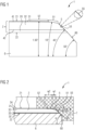
- the reverse blocking voltage can be increased by a modified shaping of the side surface of the semiconductor body.
- the first semiconductor layer is arranged between the first main surface and the first pn junction.
- the second semiconductor layer may be arranged between the first pn junction and the second main surface.
- the first main surface may represent the cathode side and the second main surface may represent the anode side of the semiconductor body or vice versa.
- At least one of the first partial region and the second partial region exhibit traces of a mechanical ablation method.
- the traces are traces of a grinding method.
- bevelled side surfaces may be obtained in a reliable and efficient manner.
- Chemical methods such as etching may be dispensed with. However, chemical methods may be used instead of or in addition to mechanical ablation methods if appropriate.
- at least one of the first partial region and the second partial region exhibit traces of a laser ablation method.
- the side surface comprises a third partial region.
- the first partial region is arranged between the second partial region and the third partial region.
- the third partial region delimits the second pn junction in the lateral direction.
- the third partial region is spaced apart from the first pn junction in vertical direction.
- the third angle is between 20° and 60° inclusive.
- the third partial region forms a positive bevel for the second pn junction, for example.
- a negative bevel may be used for the second pn junction.
- the semiconductor device is a thyristor.
- the thyristor is configured as a phase control thyristor (PCT).
- PCT phase control thyristor
- the described configuration of the side surface having different partial regions may also apply for other semiconductor devices with a pn junction.
- the first angle ⁇ (cf. Figure 2 ) is between 5° and 20° inclusive, for instance, for example 10° or 14°.
- the second angle ⁇ is between 0.8° and 5° inclusive, for instance, for example 1°.
- the grinding may be performed such that also material of the carrier 6 is removed so that at least part of a side surface 60 of the carrier 6 has the same angle with respect to the first pn junction 41 as the third partial region 53.
- Other ablation methods may also be used, for example a laser ablation method, resulting in characteristic traces 55.
- the semiconductor body 2 When seen from the first main surface 21 towards the second main surface 22, the semiconductor body 2 comprises a fourth semiconductor layer 34 acting as an n + layer, the first semiconductor layer 31 as p-layer, the second semiconductor layer 32 as n - layer, the third semiconductor layer 33 as p-layer and a fifth semiconductor layer 35 as a p + layer.
- the side surface 5 of the semiconductor body 2 is surrounded by an insulator 7, such as rubber, in order to protect the otherwise exposed first and second pn junctions 41, 42 at the side surface 5.
- Figure 3A illustrates results of electrical simulations of the electrical field for a semiconductor device as described in connection with Figure 2 at a voltage of 7 kV applied in reverse direction.
- the simulation is based on a device with a first angle ⁇ of 10°.
Landscapes
- Thyristors (AREA)
Claims (9)
- Halbleiterbauelement (1) mit einem Halbleiterkörper (2), wobei sich der Halbleiterkörper (2) in einer vertikalen Richtung zwischen einer ersten Hauptoberfläche (21) und einer der ersten Hauptoberfläche (21) gegenüber liegenden zweiten Hauptoberfläche (22) erstreckt, wobei- der Halbleiterkörper (2) eine erste Halbleiterschicht (31) eines ersten Leitfähigkeitstyps und eine zweite Halbleiterschicht (32) eines vom ersten Leitfähigkeitstyp verschiedenen zweiten Leitfähigkeitstyps aufweist, wodurch ein erster pn-Übergang (41) gebildet ist;- die erste Halbleiterschicht (31) stärker dotiert ist als die zweite Halbleiterschicht (32);- eine Seitenfläche (5) des Halbleiterkörpers (2), die sich zwischen der ersten Hauptoberfläche (21) und der zweiten Hauptoberfläche (22) erstreckt, den Halbleiterkörper (2) in einer lateralen Richtung begrenzt;- die Seitenfläche (5) des Halbleiterkörpers (2) einen ersten Teilbereich (51) und einen zweiten Teilbereich (52) aufweist;- der erste Teilbereich (51) und der zweite Teilbereich (52) die erste Halbleiterschicht (31) bereichsweise begrenzen;- der erste Teilbereich (51) den ersten pn-Übergang (41) in der lateralen Richtung begrenzt;- der zweite Teilbereich (52) in vertikaler Richtung von dem ersten pn-Übergang (41) beabstandet ist; und- der erste Teilbereich (51) in einem ersten Winkel (α) angeordnet ist und der zweite Teilbereich (52) in einem zweiten Winkel (β) in Bezug auf den ersten pn-Übergang (41) angeordnet ist, wobei der erste Winkel (α) größer ist als der zweite Winkel (β);- die Seitenfläche (5) einen dritten Teilbereich (53) aufweist, wobei der erste Teilbereich (51) zwischen dem zweiten Teilbereich (52) und dem dritten Teilbereich (53) angeordnet ist, wobei der dritte Teilbereich (53) direkt an den ersten Teilbereich (51) angrenzt;- der Halbleiterkörper (2) ferner einen zweiten pn-Übergang (42) aufweist, wobei der dritte Teilbereich (53) den zweiten pn-Übergang (42) in der lateralen Richtung begrenzt; und- der dritte Teilbereich (53) in einem dritten Winkel (γ) in Bezug auf den ersten pn-Übergang (41) angeordnet ist, wobei der dritte Winkel (γ) größer ist als der erste Winkel (α); und- der dritte Winkel (γ) zwischen einschließlich 20° und 60° liegt; und- der erste Winkel (α) innerhalb des ersten Teilbereichs (51) konstant ist, der zweite Winkel (β) innerhalb des zweiten Teilbereichs (52) konstant ist und der dritte Winkel (γ) innerhalb des dritten Teilbereichs (53) konstant ist.
- Das Halbleiterbauelement (1) nach Anspruch 1,
wobei der erste Winkel (α) zwischen einschließlich 5° und 20° liegt. - Das Halbleiterbauelement nach Anspruch 1 oder 2,
wobei der zweite Winkel (β) zwischen einschließlich 0,8° und 5° liegt. - Halbleiterbauelement (1) nach einem der vorhergehenden Ansprüche,
wobei eine seitliche Erstreckung (w1) des ersten Teilbereichs (51) kleiner ist als eine seitliche Erstreckung (w2) des zweiten Teilbereichs (52), gesehen in vertikaler Richtung. - Halbleiterbauelement (1) nach einem der vorhergehenden Ansprüche,
wobei der erste Teilbereich (51) und der zweite Teilbereich (52) Spuren (55) eines mechanischen Abtragsverfahrens aufweisen. - Das Halbleiterbauelement (1) nach einem der Ansprüche 1 bis 4,
wobei der erste Teilbereich (51) und der zweite Teilbereich (52) Spuren (55) eines Laserabtragsverfahrens aufweisen. - Das Halbleiterbauelement (1) nach einem der vorhergehenden Ansprüche,
wobei der zweite pn-Übergang (42) zwischen der zweiten Halbleiterschicht (32) und einer dritten Halbleiterschicht (33) des ersten Leitfähigkeitstyps ausgebildet ist. - Halbleiterbauelement (1) nach einem der vorangehenden Ansprüche,
wobei das Halbleiterbauelement (1) ein Thyristor ist. - Das Halbleiterbauelement (1) nach Anspruch 8,
wobei der Thyristor eine positiv-negative Abschrägungsform aufweist, wobei die negative Abschrägung den ersten und zweiten Teilbereich umfasst.
Priority Applications (5)
| Application Number | Priority Date | Filing Date | Title |
|---|---|---|---|
| EP20210372.7A EP4006990B1 (de) | 2020-11-27 | 2020-11-27 | Halbleiterbauelement mit einer seitenfläche mit unterschiedlichen teilbereichen |
| JP2023532389A JP7432100B2 (ja) | 2020-11-27 | 2021-11-16 | 異なる部分領域を有する側面を備えた半導体装置 |
| CN202180079853.7A CN116569341B (zh) | 2020-11-27 | 2021-11-16 | 带有具有不同局部区域的侧表面的半导体器件 |
| PCT/EP2021/081856 WO2022112059A1 (en) | 2020-11-27 | 2021-11-16 | Semiconductor device with a side surface having different partial regions |
| US18/038,845 US12513949B2 (en) | 2020-11-27 | 2021-11-16 | Semiconductor device with a side surface having different partial regions |
Applications Claiming Priority (1)
| Application Number | Priority Date | Filing Date | Title |
|---|---|---|---|
| EP20210372.7A EP4006990B1 (de) | 2020-11-27 | 2020-11-27 | Halbleiterbauelement mit einer seitenfläche mit unterschiedlichen teilbereichen |
Publications (2)
| Publication Number | Publication Date |
|---|---|
| EP4006990A1 EP4006990A1 (de) | 2022-06-01 |
| EP4006990B1 true EP4006990B1 (de) | 2023-04-05 |
Family
ID=73642707
Family Applications (1)
| Application Number | Title | Priority Date | Filing Date |
|---|---|---|---|
| EP20210372.7A Active EP4006990B1 (de) | 2020-11-27 | 2020-11-27 | Halbleiterbauelement mit einer seitenfläche mit unterschiedlichen teilbereichen |
Country Status (5)
| Country | Link |
|---|---|
| US (1) | US12513949B2 (de) |
| EP (1) | EP4006990B1 (de) |
| JP (1) | JP7432100B2 (de) |
| CN (1) | CN116569341B (de) |
| WO (1) | WO2022112059A1 (de) |
Family Cites Families (25)
| Publication number | Priority date | Publication date | Assignee | Title |
|---|---|---|---|---|
| NL280641A (de) | 1961-07-07 | |||
| GB1052661A (de) | 1963-01-30 | 1900-01-01 | ||
| US3575644A (en) | 1963-01-30 | 1971-04-20 | Gen Electric | Semiconductor device with double positive bevel |
| US3255055A (en) | 1963-03-20 | 1966-06-07 | Hoffman Electronics Corp | Semiconductor device |
| NL6603372A (de) | 1965-03-25 | 1966-09-26 | ||
| US3579060A (en) * | 1969-03-21 | 1971-05-18 | Gen Electric | Thyristor with improved current and voltage handling characteristics |
| DE7328984U (de) * | 1973-07-06 | 1975-05-15 | Bbc Ag Brown Boveri & Cie | Leistungshalbleiterbauelement |
| JPS54163883U (de) * | 1978-05-09 | 1979-11-16 | ||
| JPS54163883A (en) | 1978-06-13 | 1979-12-26 | Mitsubishi Chem Ind | Improvement of yeast variety |
| JPS60224268A (ja) * | 1984-04-20 | 1985-11-08 | Meidensha Electric Mfg Co Ltd | 電力用半導体素子 |
| JPS6279667A (ja) * | 1985-10-03 | 1987-04-13 | Mitsubishi Electric Corp | 半導体装置 |
| JP2603083B2 (ja) * | 1987-10-02 | 1997-04-23 | 財団法人半導体研究振興会 | 高耐圧半導体素子 |
| JP2651678B2 (ja) * | 1987-10-02 | 1997-09-10 | 財団法人半導体研究振興会 | 高耐圧半導体素子及びその製造方法 |
| EP0532941B1 (de) * | 1991-09-20 | 1995-08-09 | eupec Europäische Gesellschaft für Leistungshalbleiter mbH & Co. KG | Thyristor mit Randstruktur |
| JPH08242009A (ja) * | 1994-12-02 | 1996-09-17 | Eurec Europ G Fur Leistungshalbleiter Mbh & Co Kg | パワー半導体デバイス |
| DE69626299T2 (de) | 1996-09-24 | 2003-12-11 | Mitsubishi Denki K.K., Tokio/Tokyo | Halbleiteranordnung und verfahren zur herstellung |
| DE10250608B4 (de) | 2002-10-30 | 2005-09-29 | eupec Europäische Gesellschaft für Leistungshalbleiter mbH | Thyristorbauelement mit verbessertem Sperrverhalten in Rückwärtsrichtung |
| US7205583B1 (en) | 2005-12-22 | 2007-04-17 | Semiconductor Components Industries, L.L.C. | Thyristor and method of manufacture |
| JP6026418B2 (ja) | 2010-09-27 | 2016-11-16 | アーベーベー・テヒノロギー・アーゲー | バイポーラノンパンチスルー電力半導体デバイス |
| EP2447988B1 (de) | 2010-11-02 | 2015-05-06 | GE Energy Power Conversion Technology Limited | Leistungselektronikvorrichtung mit Randpassivierung |
| US20140151841A1 (en) * | 2012-12-01 | 2014-06-05 | North Carolina State University | Semiconductor devices having a positive-bevel termination or a negative-bevel termination and their manufacture |
| JP6742894B2 (ja) | 2016-06-09 | 2020-08-19 | 株式会社日立製作所 | データ予測システムおよびデータ予測方法 |
| DE102016124670B4 (de) | 2016-12-16 | 2020-01-23 | Semikron Elektronik Gmbh & Co. Kg | Thyristor mit einem Halbleiterkörper |
| WO2019158594A1 (en) | 2018-02-13 | 2019-08-22 | Abb Schweiz Ag | Bidirectional thyristor device |
| JP2025163883A (ja) | 2024-04-18 | 2025-10-30 | 株式会社デンソーテン | 車両制御装置、車両制御方法および車両 |
-
2020
- 2020-11-27 EP EP20210372.7A patent/EP4006990B1/de active Active
-
2021
- 2021-11-16 CN CN202180079853.7A patent/CN116569341B/zh active Active
- 2021-11-16 US US18/038,845 patent/US12513949B2/en active Active
- 2021-11-16 WO PCT/EP2021/081856 patent/WO2022112059A1/en not_active Ceased
- 2021-11-16 JP JP2023532389A patent/JP7432100B2/ja active Active
Also Published As
| Publication number | Publication date |
|---|---|
| EP4006990A1 (de) | 2022-06-01 |
| US12513949B2 (en) | 2025-12-30 |
| CN116569341B (zh) | 2024-05-14 |
| CN116569341A (zh) | 2023-08-08 |
| US20240021672A1 (en) | 2024-01-18 |
| JP2023545217A (ja) | 2023-10-26 |
| JP7432100B2 (ja) | 2024-02-16 |
| WO2022112059A1 (en) | 2022-06-02 |
Similar Documents
| Publication | Publication Date | Title |
|---|---|---|
| JP7724284B2 (ja) | 信頼性及び導通が向上したトレンチ型パワー・デバイス | |
| US6104062A (en) | Semiconductor device having reduced effective substrate resistivity and associated methods | |
| US10256314B2 (en) | Semiconductor device | |
| CN101221989B (zh) | SiC肖特基势垒半导体器件 | |
| CN106531813B (zh) | 半导体装置 | |
| US9337186B2 (en) | Semiconductor device and a method for manufacturing a semiconductor device having a semi-insulating region | |
| EP3353814B1 (de) | Flächeneffizienter abschluss mit schwebenden feldringen | |
| CN103872099B (zh) | 具有阶梯状边缘终端的半导体器件,以及用于制造半导体器件的方法 | |
| CN108292669B (zh) | 关断型功率半导体器件及其制造方法 | |
| CN102694014A (zh) | 半导体装置及其制造方法 | |
| US20150048489A1 (en) | Edge termination technique for high voltage power devices | |
| JP6337217B1 (ja) | 厚い上部金属設計を有するパワー半導体デバイスおよびそのパワー半導体デバイスの製造方法 | |
| EP3154091A1 (de) | Rückwärtsleitendes halbleiterbauelement | |
| EP2960941B1 (de) | Rückwärtsleitendes Hochleistungshalbleiterbauelement | |
| US20150255290A1 (en) | Method for manufacturing semiconductor device | |
| EP4439633A1 (de) | Leistungshalbleiterbauelement und verfahren zur herstellung eines leistungshalbleiterbauelements | |
| WO1999052152A1 (fr) | Dispositif semi-conducteur et convertisseur de puissance | |
| US12513949B2 (en) | Semiconductor device with a side surface having different partial regions | |
| JP2005223349A (ja) | 高耐圧半導体装置及びこれを用いた電力変換器 | |
| JP2015510272A (ja) | 負ベベルにより終端した、高い阻止電圧を有するSiC素子 | |
| US20070042549A1 (en) | Semiconductor device having reduced effective substrate resistivity and associated methods | |
| KR102170068B1 (ko) | 바이폴라 논-펀치-스루 전력 반도체 디바이스 | |
| JP2018201050A (ja) | 半導体装置 | |
| US20260032973A1 (en) | Gate trench power semiconductor devices having shallow trench shields and deep support shields | |
| CN121986570A (zh) | 具有减小单元节距和导通状态电阻的成形深支撑屏蔽件的栅极沟槽功率半导体器件 |
Legal Events
| Date | Code | Title | Description |
|---|---|---|---|
| PUAI | Public reference made under article 153(3) epc to a published international application that has entered the european phase |
Free format text: ORIGINAL CODE: 0009012 |
|
| STAA | Information on the status of an ep patent application or granted ep patent |
Free format text: STATUS: THE APPLICATION HAS BEEN PUBLISHED |
|
| AK | Designated contracting states |
Kind code of ref document: A1 Designated state(s): AL AT BE BG CH CY CZ DE DK EE ES FI FR GB GR HR HU IE IS IT LI LT LU LV MC MK MT NL NO PL PT RO RS SE SI SK SM TR |
|
| RIN1 | Information on inventor provided before grant (corrected) |
Inventor name: JAGODA, DOBRZYNSKA Inventor name: AKURATI, KRANTHI KUMAR Inventor name: COMMIN, PAUL |
|
| STAA | Information on the status of an ep patent application or granted ep patent |
Free format text: STATUS: REQUEST FOR EXAMINATION WAS MADE |
|
| 17P | Request for examination filed |
Effective date: 20220726 |
|
| RBV | Designated contracting states (corrected) |
Designated state(s): AL AT BE BG CH CY CZ DE DK EE ES FI FR GB GR HR HU IE IS IT LI LT LU LV MC MK MT NL NO PL PT RO RS SE SI SK SM TR |
|
| GRAP | Despatch of communication of intention to grant a patent |
Free format text: ORIGINAL CODE: EPIDOSNIGR1 |
|
| STAA | Information on the status of an ep patent application or granted ep patent |
Free format text: STATUS: GRANT OF PATENT IS INTENDED |
|
| INTG | Intention to grant announced |
Effective date: 20221201 |
|
| GRAS | Grant fee paid |
Free format text: ORIGINAL CODE: EPIDOSNIGR3 |
|
| GRAA | (expected) grant |
Free format text: ORIGINAL CODE: 0009210 |
|
| STAA | Information on the status of an ep patent application or granted ep patent |
Free format text: STATUS: THE PATENT HAS BEEN GRANTED |
|
| AK | Designated contracting states |
Kind code of ref document: B1 Designated state(s): AL AT BE BG CH CY CZ DE DK EE ES FI FR GB GR HR HU IE IS IT LI LT LU LV MC MK MT NL NO PL PT RO RS SE SI SK SM TR |
|
| REG | Reference to a national code |
Ref country code: GB Ref legal event code: FG4D |
|
| REG | Reference to a national code |
Ref country code: DE Ref legal event code: R096 Ref document number: 602020009437 Country of ref document: DE |
|
| REG | Reference to a national code |
Ref country code: CH Ref legal event code: EP |
|
| REG | Reference to a national code |
Ref country code: AT Ref legal event code: REF Ref document number: 1558907 Country of ref document: AT Kind code of ref document: T Effective date: 20230415 |
|
| REG | Reference to a national code |
Ref country code: IE Ref legal event code: FG4D |
|
| P01 | Opt-out of the competence of the unified patent court (upc) registered |
Effective date: 20230527 |
|
| REG | Reference to a national code |
Ref country code: LT Ref legal event code: MG9D |
|
| REG | Reference to a national code |
Ref country code: NL Ref legal event code: MP Effective date: 20230405 |
|
| REG | Reference to a national code |
Ref country code: AT Ref legal event code: MK05 Ref document number: 1558907 Country of ref document: AT Kind code of ref document: T Effective date: 20230405 |
|
| PG25 | Lapsed in a contracting state [announced via postgrant information from national office to epo] |
Ref country code: NL Free format text: LAPSE BECAUSE OF FAILURE TO SUBMIT A TRANSLATION OF THE DESCRIPTION OR TO PAY THE FEE WITHIN THE PRESCRIBED TIME-LIMIT Effective date: 20230405 |
|
| PG25 | Lapsed in a contracting state [announced via postgrant information from national office to epo] |
Ref country code: SE Free format text: LAPSE BECAUSE OF FAILURE TO SUBMIT A TRANSLATION OF THE DESCRIPTION OR TO PAY THE FEE WITHIN THE PRESCRIBED TIME-LIMIT Effective date: 20230405 Ref country code: PT Free format text: LAPSE BECAUSE OF FAILURE TO SUBMIT A TRANSLATION OF THE DESCRIPTION OR TO PAY THE FEE WITHIN THE PRESCRIBED TIME-LIMIT Effective date: 20230807 Ref country code: NO Free format text: LAPSE BECAUSE OF FAILURE TO SUBMIT A TRANSLATION OF THE DESCRIPTION OR TO PAY THE FEE WITHIN THE PRESCRIBED TIME-LIMIT Effective date: 20230705 Ref country code: ES Free format text: LAPSE BECAUSE OF FAILURE TO SUBMIT A TRANSLATION OF THE DESCRIPTION OR TO PAY THE FEE WITHIN THE PRESCRIBED TIME-LIMIT Effective date: 20230405 Ref country code: AT Free format text: LAPSE BECAUSE OF FAILURE TO SUBMIT A TRANSLATION OF THE DESCRIPTION OR TO PAY THE FEE WITHIN THE PRESCRIBED TIME-LIMIT Effective date: 20230405 |
|
| PG25 | Lapsed in a contracting state [announced via postgrant information from national office to epo] |
Ref country code: RS Free format text: LAPSE BECAUSE OF FAILURE TO SUBMIT A TRANSLATION OF THE DESCRIPTION OR TO PAY THE FEE WITHIN THE PRESCRIBED TIME-LIMIT Effective date: 20230405 Ref country code: PL Free format text: LAPSE BECAUSE OF FAILURE TO SUBMIT A TRANSLATION OF THE DESCRIPTION OR TO PAY THE FEE WITHIN THE PRESCRIBED TIME-LIMIT Effective date: 20230405 Ref country code: LV Free format text: LAPSE BECAUSE OF FAILURE TO SUBMIT A TRANSLATION OF THE DESCRIPTION OR TO PAY THE FEE WITHIN THE PRESCRIBED TIME-LIMIT Effective date: 20230405 Ref country code: LT Free format text: LAPSE BECAUSE OF FAILURE TO SUBMIT A TRANSLATION OF THE DESCRIPTION OR TO PAY THE FEE WITHIN THE PRESCRIBED TIME-LIMIT Effective date: 20230405 Ref country code: IS Free format text: LAPSE BECAUSE OF FAILURE TO SUBMIT A TRANSLATION OF THE DESCRIPTION OR TO PAY THE FEE WITHIN THE PRESCRIBED TIME-LIMIT Effective date: 20230805 Ref country code: HR Free format text: LAPSE BECAUSE OF FAILURE TO SUBMIT A TRANSLATION OF THE DESCRIPTION OR TO PAY THE FEE WITHIN THE PRESCRIBED TIME-LIMIT Effective date: 20230405 Ref country code: GR Free format text: LAPSE BECAUSE OF FAILURE TO SUBMIT A TRANSLATION OF THE DESCRIPTION OR TO PAY THE FEE WITHIN THE PRESCRIBED TIME-LIMIT Effective date: 20230706 Ref country code: AL Free format text: LAPSE BECAUSE OF FAILURE TO SUBMIT A TRANSLATION OF THE DESCRIPTION OR TO PAY THE FEE WITHIN THE PRESCRIBED TIME-LIMIT Effective date: 20230405 |
|
| RAP2 | Party data changed (patent owner data changed or rights of a patent transferred) |
Owner name: HITACHI ENERGY LTD |
|
| PG25 | Lapsed in a contracting state [announced via postgrant information from national office to epo] |
Ref country code: FI Free format text: LAPSE BECAUSE OF FAILURE TO SUBMIT A TRANSLATION OF THE DESCRIPTION OR TO PAY THE FEE WITHIN THE PRESCRIBED TIME-LIMIT Effective date: 20230405 |
|
| REG | Reference to a national code |
Ref country code: DE Ref legal event code: R097 Ref document number: 602020009437 Country of ref document: DE |
|
| PG25 | Lapsed in a contracting state [announced via postgrant information from national office to epo] |
Ref country code: SK Free format text: LAPSE BECAUSE OF FAILURE TO SUBMIT A TRANSLATION OF THE DESCRIPTION OR TO PAY THE FEE WITHIN THE PRESCRIBED TIME-LIMIT Effective date: 20230405 |
|
| PG25 | Lapsed in a contracting state [announced via postgrant information from national office to epo] |
Ref country code: SM Free format text: LAPSE BECAUSE OF FAILURE TO SUBMIT A TRANSLATION OF THE DESCRIPTION OR TO PAY THE FEE WITHIN THE PRESCRIBED TIME-LIMIT Effective date: 20230405 Ref country code: SK Free format text: LAPSE BECAUSE OF FAILURE TO SUBMIT A TRANSLATION OF THE DESCRIPTION OR TO PAY THE FEE WITHIN THE PRESCRIBED TIME-LIMIT Effective date: 20230405 Ref country code: RO Free format text: LAPSE BECAUSE OF FAILURE TO SUBMIT A TRANSLATION OF THE DESCRIPTION OR TO PAY THE FEE WITHIN THE PRESCRIBED TIME-LIMIT Effective date: 20230405 Ref country code: EE Free format text: LAPSE BECAUSE OF FAILURE TO SUBMIT A TRANSLATION OF THE DESCRIPTION OR TO PAY THE FEE WITHIN THE PRESCRIBED TIME-LIMIT Effective date: 20230405 Ref country code: DK Free format text: LAPSE BECAUSE OF FAILURE TO SUBMIT A TRANSLATION OF THE DESCRIPTION OR TO PAY THE FEE WITHIN THE PRESCRIBED TIME-LIMIT Effective date: 20230405 Ref country code: CZ Free format text: LAPSE BECAUSE OF FAILURE TO SUBMIT A TRANSLATION OF THE DESCRIPTION OR TO PAY THE FEE WITHIN THE PRESCRIBED TIME-LIMIT Effective date: 20230405 |
|
| PLBE | No opposition filed within time limit |
Free format text: ORIGINAL CODE: 0009261 |
|
| STAA | Information on the status of an ep patent application or granted ep patent |
Free format text: STATUS: NO OPPOSITION FILED WITHIN TIME LIMIT |
|
| 26N | No opposition filed |
Effective date: 20240108 |
|
| REG | Reference to a national code |
Ref country code: DE Ref legal event code: R081 Ref document number: 602020009437 Country of ref document: DE Owner name: HITACHI ENERGY LTD, CH Free format text: FORMER OWNER: HITACHI ENERGY SWITZERLAND AG, BADEN, CH |
|
| PG25 | Lapsed in a contracting state [announced via postgrant information from national office to epo] |
Ref country code: SI Free format text: LAPSE BECAUSE OF FAILURE TO SUBMIT A TRANSLATION OF THE DESCRIPTION OR TO PAY THE FEE WITHIN THE PRESCRIBED TIME-LIMIT Effective date: 20230405 |
|
| PG25 | Lapsed in a contracting state [announced via postgrant information from national office to epo] |
Ref country code: SI Free format text: LAPSE BECAUSE OF FAILURE TO SUBMIT A TRANSLATION OF THE DESCRIPTION OR TO PAY THE FEE WITHIN THE PRESCRIBED TIME-LIMIT Effective date: 20230405 Ref country code: IT Free format text: LAPSE BECAUSE OF FAILURE TO SUBMIT A TRANSLATION OF THE DESCRIPTION OR TO PAY THE FEE WITHIN THE PRESCRIBED TIME-LIMIT Effective date: 20230405 |
|
| REG | Reference to a national code |
Ref country code: CH Ref legal event code: PL |
|
| PG25 | Lapsed in a contracting state [announced via postgrant information from national office to epo] |
Ref country code: MC Free format text: LAPSE BECAUSE OF FAILURE TO SUBMIT A TRANSLATION OF THE DESCRIPTION OR TO PAY THE FEE WITHIN THE PRESCRIBED TIME-LIMIT Effective date: 20230405 |
|
| PG25 | Lapsed in a contracting state [announced via postgrant information from national office to epo] |
Ref country code: LU Free format text: LAPSE BECAUSE OF NON-PAYMENT OF DUE FEES Effective date: 20231127 |
|
| PG25 | Lapsed in a contracting state [announced via postgrant information from national office to epo] |
Ref country code: CH Free format text: LAPSE BECAUSE OF NON-PAYMENT OF DUE FEES Effective date: 20231130 |
|
| PG25 | Lapsed in a contracting state [announced via postgrant information from national office to epo] |
Ref country code: MC Free format text: LAPSE BECAUSE OF FAILURE TO SUBMIT A TRANSLATION OF THE DESCRIPTION OR TO PAY THE FEE WITHIN THE PRESCRIBED TIME-LIMIT Effective date: 20230405 Ref country code: LU Free format text: LAPSE BECAUSE OF NON-PAYMENT OF DUE FEES Effective date: 20231127 Ref country code: CH Free format text: LAPSE BECAUSE OF NON-PAYMENT OF DUE FEES Effective date: 20231130 |
|
| REG | Reference to a national code |
Ref country code: BE Ref legal event code: MM Effective date: 20231130 |
|
| REG | Reference to a national code |
Ref country code: GB Ref legal event code: 732E Free format text: REGISTERED BETWEEN 20240718 AND 20240724 |
|
| REG | Reference to a national code |
Ref country code: IE Ref legal event code: MM4A |
|
| PG25 | Lapsed in a contracting state [announced via postgrant information from national office to epo] |
Ref country code: IE Free format text: LAPSE BECAUSE OF NON-PAYMENT OF DUE FEES Effective date: 20231127 |
|
| PG25 | Lapsed in a contracting state [announced via postgrant information from national office to epo] |
Ref country code: BE Free format text: LAPSE BECAUSE OF NON-PAYMENT OF DUE FEES Effective date: 20231130 |
|
| PG25 | Lapsed in a contracting state [announced via postgrant information from national office to epo] |
Ref country code: FR Free format text: LAPSE BECAUSE OF NON-PAYMENT OF DUE FEES Effective date: 20231130 |
|
| PG25 | Lapsed in a contracting state [announced via postgrant information from national office to epo] |
Ref country code: IE Free format text: LAPSE BECAUSE OF NON-PAYMENT OF DUE FEES Effective date: 20231127 Ref country code: FR Free format text: LAPSE BECAUSE OF NON-PAYMENT OF DUE FEES Effective date: 20231130 Ref country code: BE Free format text: LAPSE BECAUSE OF NON-PAYMENT OF DUE FEES Effective date: 20231130 |
|
| PG25 | Lapsed in a contracting state [announced via postgrant information from national office to epo] |
Ref country code: BG Free format text: LAPSE BECAUSE OF FAILURE TO SUBMIT A TRANSLATION OF THE DESCRIPTION OR TO PAY THE FEE WITHIN THE PRESCRIBED TIME-LIMIT Effective date: 20230405 |
|
| REG | Reference to a national code |
Ref country code: DE Ref legal event code: R079 Ref document number: 602020009437 Country of ref document: DE Free format text: PREVIOUS MAIN CLASS: H01L0029740000 Ipc: H10D0018000000 |
|
| PG25 | Lapsed in a contracting state [announced via postgrant information from national office to epo] |
Ref country code: BG Free format text: LAPSE BECAUSE OF FAILURE TO SUBMIT A TRANSLATION OF THE DESCRIPTION OR TO PAY THE FEE WITHIN THE PRESCRIBED TIME-LIMIT Effective date: 20230405 |
|
| REG | Reference to a national code |
Ref country code: DE Ref legal event code: R082 Ref document number: 602020009437 Country of ref document: DE Representative=s name: DENNEMEYER & ASSOCIATES RECHTSANWALTSGESELLSCH, DE |
|
| PG25 | Lapsed in a contracting state [announced via postgrant information from national office to epo] |
Ref country code: CY Free format text: LAPSE BECAUSE OF FAILURE TO SUBMIT A TRANSLATION OF THE DESCRIPTION OR TO PAY THE FEE WITHIN THE PRESCRIBED TIME-LIMIT; INVALID AB INITIO Effective date: 20201127 |
|
| PG25 | Lapsed in a contracting state [announced via postgrant information from national office to epo] |
Ref country code: HU Free format text: LAPSE BECAUSE OF FAILURE TO SUBMIT A TRANSLATION OF THE DESCRIPTION OR TO PAY THE FEE WITHIN THE PRESCRIBED TIME-LIMIT; INVALID AB INITIO Effective date: 20201127 |
|
| PG25 | Lapsed in a contracting state [announced via postgrant information from national office to epo] |
Ref country code: TR Free format text: LAPSE BECAUSE OF FAILURE TO SUBMIT A TRANSLATION OF THE DESCRIPTION OR TO PAY THE FEE WITHIN THE PRESCRIBED TIME-LIMIT Effective date: 20230405 |
|
| PGFP | Annual fee paid to national office [announced via postgrant information from national office to epo] |
Ref country code: DE Payment date: 20251119 Year of fee payment: 6 |
|
| PGFP | Annual fee paid to national office [announced via postgrant information from national office to epo] |
Ref country code: GB Payment date: 20251121 Year of fee payment: 6 |