EP4007062A1 - Doppelfrequenz-doppelpolarisationsteiler - Google Patents
Doppelfrequenz-doppelpolarisationsteiler Download PDFInfo
- Publication number
- EP4007062A1 EP4007062A1 EP19957773.5A EP19957773A EP4007062A1 EP 4007062 A1 EP4007062 A1 EP 4007062A1 EP 19957773 A EP19957773 A EP 19957773A EP 4007062 A1 EP4007062 A1 EP 4007062A1
- Authority
- EP
- European Patent Office
- Prior art keywords
- waveguide
- magic
- dual
- cross
- plane
- Prior art date
- Legal status (The legal status is an assumption and is not a legal conclusion. Google has not performed a legal analysis and makes no representation as to the accuracy of the status listed.)
- Granted
Links
Images


Classifications
-
- H—ELECTRICITY
- H01—ELECTRIC ELEMENTS
- H01P—WAVEGUIDES; RESONATORS, LINES, OR OTHER DEVICES OF THE WAVEGUIDE TYPE
- H01P5/00—Coupling devices of the waveguide type
- H01P5/12—Coupling devices having more than two ports
- H01P5/16—Conjugate devices, i.e. devices having at least one port decoupled from one other port
-
- H—ELECTRICITY
- H01—ELECTRIC ELEMENTS
- H01P—WAVEGUIDES; RESONATORS, LINES, OR OTHER DEVICES OF THE WAVEGUIDE TYPE
- H01P5/00—Coupling devices of the waveguide type
- H01P5/12—Coupling devices having more than two ports
- H01P5/16—Conjugate devices, i.e. devices having at least one port decoupled from one other port
- H01P5/19—Conjugate devices, i.e. devices having at least one port decoupled from one other port of the junction type
- H01P5/20—Magic-T junctions
-
- H—ELECTRICITY
- H01—ELECTRIC ELEMENTS
- H01P—WAVEGUIDES; RESONATORS, LINES, OR OTHER DEVICES OF THE WAVEGUIDE TYPE
- H01P1/00—Auxiliary devices
- H01P1/16—Auxiliary devices for mode selection, e.g. mode suppression or mode promotion; for mode conversion
- H01P1/161—Auxiliary devices for mode selection, e.g. mode suppression or mode promotion; for mode conversion sustaining two independent orthogonal modes, e.g. orthomode transducer
-
- H—ELECTRICITY
- H01—ELECTRIC ELEMENTS
- H01P—WAVEGUIDES; RESONATORS, LINES, OR OTHER DEVICES OF THE WAVEGUIDE TYPE
- H01P1/00—Auxiliary devices
- H01P1/165—Auxiliary devices for rotating the plane of polarisation
-
- H—ELECTRICITY
- H01—ELECTRIC ELEMENTS
- H01P—WAVEGUIDES; RESONATORS, LINES, OR OTHER DEVICES OF THE WAVEGUIDE TYPE
- H01P3/00—Waveguides; Transmission lines of the waveguide type
- H01P3/02—Waveguides; Transmission lines of the waveguide type with two longitudinal conductors
- H01P3/06—Coaxial lines
Definitions
- the present invention relates to the technical field of wireless communication, and, more specifically, to a dual-frequency dual-polarization splitter.
- Transceiving sharing technology has been widely used in the fields of navigation measurement and control, satellite communication, etc., and with the increase of satellite spectrum resources, an antenna used in two or more frequency bands can be implemented by the dual-frequency sharing or multi-frequency sharing antenna with only a small increase in cost, especially when the antenna aperture is large, this method can significantly reduce the cost of the antenna system, reduce the land use area, and facilitate the deployment of user sites.
- the available bandwidth of the coupling waveguide port of the coaxial turnstile coupler is getting wider and wider, which can meet the bandwidth requirements of dual-band usage.
- the coaxial inner conductor of the coaxial turnstile coupler is hollow, a circular waveguide can be formed for transmitting signals of higher frequency bands, does not need to be debugged and the structure thereof is simple.
- the C.N. Patent No. CN201711361522.4 discloses a coaxial waveguide ortho-mode coupler matched with a truncated cone, as shown in Fig. 1 , including a coaxial turnstile joint 1, a first U-shaped curved waveguide element 2, a second U-shaped curved waveguide element 3, a third U-shaped curved waveguide element 4, a fourth U-shaped curved waveguide element 5,and a first power combiner/distributor 6,and a second power combiner/distributor7, this solution has excellent electric performance, simple machining process, excellent VSWR, isolation, insertion loss and other indicators and can achieve isophase polarization separation within nearly one octave.
- the structural layout is not convenient for product realization, for example, the high-frequency signal from the coaxial turnstile joint 1 is blocked by the waveguide cavity surrounded by four U-shaped curved waveguide elements and cannot be transmitted, and the processing of product parts is also not convenient to be achieved, the intersection of the waveguide cavities in the above document is not easy to achieve during the processing of the parts; in addition, the electrical functions are not flexible enough to achieve the flexible switching between single-polarization mode and dual-polarization mode, such as signals from power combiner/divider 6,7 are in a single polarization mode.
- the purpose of the present invention is to overcome the defects of the prior art and provide a dual-frequency dual-polarization splitter.
- a dual-frequency dual-polarization splitter comprises a coaxial circular waveguide, a cross-shaped waveguide power divider, a first waveguide magic T, a second waveguide magic T and an ortho-mode transition,
- the first waveguide magic T is a first E-plane waveguide magic T
- the second waveguide magic T is a second E-plane waveguide magic T
- the first waveguide magic T is a first H-plane waveguide magic T
- the second waveguide magic T is a second H-plane waveguide magic T.
- a polarization converter is arranged between the second E-plane waveguide magic T and the ortho-mode transition.
- the first waveguide magic T and the second waveguide magic T are located on the same plane, and do not intersect to each other.
- the splitter further comprises a plurality of 90° curved waveguides, and signal channels of the cross-shaped waveguide power divider are in communication with an input port of corresponding waveguide magic T through the 90° curved waveguides.
- the 90° curved waveguide includes an E-plane 90° waveguide and an H-plane 90° curved waveguide, and an end of the E-plane 90° waveguide is in communication with a signal channel of the cross-shaped waveguide power divider, the other end of the E-plane 90° waveguide is in communication with an end of the H-plane 90° curved waveguide, and the other end of the H-plane 90° curved waveguide is in communication with an input port of the waveguide magic T.
- the dual-frequency dual-polarization splitter further includes a circular waveguide, and the circular waveguide is in communication with the circular waveguide interface.
- the outer circular waveguide transmits only the TEM mode and the TE11 mode, and cutoff other high-order mode.
- a dual-frequency dual-polarization splitter comprises an upper structure, a lower structure, a middle structure between the upper structure and the lower structure, and a cylindrical tube penetrating through the upper structure, the middle structure and the lower structures,
- the upper end surface of the middle structure is further provided with a first step corresponding to the cross-shaped waveguide cavity, and the first step is distributed in a cross shape, and the first step is connected to an outer wall of the cylindrical tube.
- the ends of the cross-shaped waveguide cavity corresponding to the four through holes are each provided with a second step.
- the step level number of the second step 104 is 2 to 4.
- a polarization converter is formed between the lower end surface of the middle structure and the upper end surface of the lower structure, and the polarization converter is arranged between the second waveguide magic T and the ortho-mode transition.
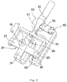
- a dual-frequency dual-polarization splitter disclosed in the preferred embodiment of the present invention includes a coaxial circular waveguide 10, a cross-shaped waveguide power divider 20, a first E-plane waveguide magic T 30, a second E-plane waveguide magic T 40, an ortho-mode transition 50, a polarization converter 60 and a circular waveguide 70, wherein the coaxial circular waveguide 10 is located on the central axis of the cross-shaped waveguide power divider 20, which is coaxial with the cross-shaped waveguide power divider 20 and perpendicular to the top surface of the cross-shaped waveguide power divider 20.
- the coaxial circular waveguide 10 includes an outer circular waveguide 11 and an inner circular waveguide 12 arranged coaxially, the inner circular waveguide 12 is located in the outer circular waveguide 11 and penetrates through the top and bottom surfaces of the cross-shaped waveguide power divider 20, that is, the lower end of the inner circular waveguide 12 penetrates through the bottom surface of the cross-shaped waveguide power divider 20, an end (such as the lower end) of the inner circular waveguide 12 is connected to a high-frequency transmitter (not shown), and the other end (such as the top end) of the inner circular waveguide 12 is connected to the antenna reflection surface (not shown) to transmit high-frequency signals to the antenna reflection surface.
- the ratio of the inner diameter of the outer circular waveguide 11 to the outer diameter of the inner circular waveguide 12 satisfies to transmit only the TEM mode and the TE11 mode and cutoff other high-order mode.
- a cross-shaped waveguide cavity 21 is formed in the cross-shaped waveguide power divider 20, and the outer circular waveguide 11 of the coaxial circular waveguide is in communication with the cross-shaped waveguide cavity 21.
- the cross-shaped waveguide power divider 20 has four signal channels distributed in a cross shape, the four signal channels are formed by extending forward, back, left, and right from the outer edge of the cross-shaped waveguide cavity 21 separately, and the four signal channels are all in communication with the cross-shaped waveguide cavity 21.
- the four signal channels are defined as a front signal channel 22, a rear signal channel 23, a left signal channel 24, and a right signal channel 25, wherein the front signal channel 22 and the rear signal channel 23 are located in the same direction (defined as a first direction), the left signal channel 24 and the right signal channel 25 are located in the same direction (defined as a second direction perpendicular to the first direction).
- the front signal channel 22 and the rear signal channel 23 are respectively in communication with two input ports 31 of the first E-plane waveguide magic T 30, and the output port 32 of the first E-plane waveguide magic T 30 is in communication with the rectangular waveguide port 51 of the ortho-mode transition 50 to merge the front and back signal channels 22, 23 into one channel.
- the left signal channel 24 and the right signal channel 25 are respectively in communication with two input ports 41 of the second E-plane waveguide magic T 40, and the output port 42 of the second E-plane waveguide magic T 40 is in communication with another rectangular waveguide port 52 of the ortho-mode transition 50 to merge the left and right signal channels 24, 25 into one channel.
- the first E-plane waveguide T 30 and the second E-plane waveguide T 40 are located on the same plane, and they do not intersect to each other.
- the two input ports 31 of the first E-plane magic T 30 are connect with the front signal channel 22 and the rear signal channel 23 by a 90° curved waveguide
- the two input ports 41 of the second E-plane magic T 40 are connected with the left signal channel 24 and the right signal channel 25 by a 90° curved waveguide.
- the four signal channels and the input ports of the corresponding E-plane waveguide magics T are all connected by E-plane 90° waveguides 80 and H-plane 90° curved waveguides 90.
- the front signal channel 22 is in communication with one end of the E-plane 90° waveguide 80, the other end of the E-plane 90° waveguide 80 is in communication with one end of the H-plane 90° curved waveguide 90, and the other end of the H-plane 90° curved waveguide 90 is in communication with the input port 31 of the first E-plane waveguide magic T 30.
- the rear signal channel 23 is in communication with one end of the E-plane 90° waveguide, the other end of the E-plane 90° waveguide 80 is in communication with one end of the H-plane 90° curved waveguide 90, and the other end of the H-plane 90° curved waveguide 90 is in communication with the other input port 31 of the first E-plane waveguide magic T 30.
- the left signal channel 24 is in communication with one end of the E-plane 90° waveguide 80
- the other end of the E-plane 90° waveguide 80 is in communication with one end of the H-plane 90° curved waveguide 90
- the other end of the H-plane 90° curved waveguide 90 is in communication with the input port 41 of the second E-plane waveguide magic T 40.
- the right signal channel 25 is in communication with one end of the E-plane 90° waveguide 80, the other end of the E-plane 90° waveguide 80 is in communication with one end of the H-plane 90° curved waveguide 90, and the other end of the H-plane 90° curved waveguide 90 is in communication with the other input port 41 of the two E-plane waveguide magic T 40.
- the four signal channels are merged into two signal channels after passing through the first E-plane waveguide magic T 30 and the second E-plane waveguide magic T 40.
- the two signal channels are respectively connected to the two rectangular waveguide ports 51 of the ortho-mode transition 50, and finally the two signal channels are merged into a circular waveguide interface 53 used to be in communication with the circular waveguide 70.
- the circular waveguide 70 is connected to a low-frequency transmitter for transmitting low-frequency signals, and the circular waveguide 70 has both horizontal polarization and vertical polarization.
- first E-plane waveguide magic T 30 and the second E-plane waveguide magic T 40 can also be replaced by the H-plane waveguide magic T, and the structure of the entire waveguide cavity needs to be modified.
- a polarization converter can be added between a channel before being merged and the ortho-mode transition 50.
- a polarization converter 60 is arranged between the output port 42 of the second E-plane waveguide magic T 40 and the ortho-mode transition 50 to reduce the complexity of the structure layout and facilitate the structural design of the product shape.
- the working principle of the present invention is: the high-frequency signal can be directly transmitted through the inner circular waveguide 12 and have both vertical and horizontal polarizations, and the low-frequency signal passes through the inner wall of the outer circular waveguide 11 and then is distributed into the signals in the four directions , front, back, left, and right by the cross-shaped waveguide power divider 20, the signals distributed in the four directions are merged into two polarization orthogonal signals through two E-plane waveguide magics T 30, 40, and the two orthogonal signals can be merged into one signal through the ortho-mode transition 50 and can transmit both vertical and horizontal polarizations at the same time.
- the present invention effectively solves the structural interference problem of coaxial circular waveguide performing high-frequency feeding and low-frequency feeding simultaneously, and reduces the length of the high-frequency transmission line and the transmission loss by the above-mentioned structural design of dividing and then merging the low frequency signal, and the clever connection layout of different types of curved waveguides.
- the present invention also realizes dual-polarization transmission in each frequency band, and can flexibly switch between vertical polarization and horizontal polarization when dual-polarization has been converted to single-polarization.
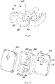
- Figs.5-7 are structural views of the specific product of the dual-frequency dual-polarization splitter of the present invention, specifically, the product includes an upper structure 100, a lower structure 300, and a middle structure 200 located between the upper structure 100 and the lower structure 300, wherein the upper structure 100 includes a first upper end surface 101 and a first lower end surface 102 opposite to each other, a cross-shaped waveguide cavity 21 is formed on the first lower end surface 102, the cross-shaped waveguide cavity 21 is recessed from the first lower end surface 102 toward the first upper end surface 101, a circular hole 103 is provided at the center of the cross-shaped waveguide cavity 21, and the circular hole 103 penetrates through the first upper end surface 101 and the first lower end surface 102 of the upper structure 100.
- the upper structure 100 includes a first upper end surface 101 and a first lower end surface 102 opposite to each other
- a cross-shaped waveguide cavity 21 is formed on the first lower end surface 102
- the cross-shaped waveguide cavity 21 is recessed from the first lower end surface
- the middle structure 200 has a second upper end surface 201 and a second lower end surface 202 opposite to each other, wherein the second upper end surface 201 is the end surface close to the first lower end surface 102 of the upper structure 100.
- a cylindrical tube 203 is fixed on the second upper end surface 201, the cylindrical tube 203 is perpendicular to the second upper end surface 201 of the middle structure 200, and the cylindrical tube 203 extends upward to the first upper end surface 101 of the upper structure 100 through the circular hole 103 of the upper structure 100, the cylindrical tube 203 is coaxial with the circular hole 103, so that the cylindrical tube 203 and the circular hole 103 form a inner circular waveguide 12 and an outer circular waveguide 11 coaxially.
- the cylindrical tube 203 also penetrates through the lower structure 300, that is, the cylindrical tube 203 penetrates through the upper structure 100, the middle structure 200 and the lower structure 300.
- a first step 26 is further provided on the second upper end surface 201 of the middle structure 200, the first step 26 corresponding to the cross-shaped waveguide cavity 21 is also distributed in a cross shape, and the distribution direction of the cross shape is the same as that of the cross-shaped waveguide cavity 21, the cylindrical tube 203 is located at the center of the first step 26, and the first step 26 is connected to the outer wall of the cylindrical tube 203.
- the first step 26 is used to optimize the impedance matching of the four ports of the cross-shaped waveguide power divider 20 to increase the working bandwidth.
- a through hole 204 penetrating through the middle structure 200 is provided at a certain distance from the end of the first step 26, the first step 26 has four ends, correspondingly, four through holes 206 are formed, the four through holes 206 are in communication with the cross-shaped waveguide cavity 21, specifically, the four output ports of the cross-shaped waveguide cavity 21 respectively.
- the four ends of the cross-shaped waveguide cavity 21 corresponding to the four through holes 204 are each provided with a second step 104, and the step extension direction of the second step 104 is from the bottom of the cross-shaped waveguide cavity 21 to the first lower end surface 102 of the upper structure 100, the step level number of the second step 104 is usually 2 to 4.
- the arrangement of the second step 104 facilitates the transition of the signal from the cross-shaped waveguide cavity 21 to the corresponding through hole 204.
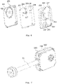
- the second lower end surface 202 of the middle structure 200 and he third upper end surface 301 of the lower structure 300 are each provided with a half of the first low-frequency waveguide cavity 205, a half of the second low-frequency waveguide cavity 206, and a half of the ortho-mode conversion cavity 207 in corresponding positions.
- the first low-frequency waveguide cavities 205 on the middle structure 200 and the lower structure 300 are combined to form the first E-plane waveguide magic T 30, and the second low-frequency waveguide cavities 206 on the middle structure 200 and the lower structure 300 are combined to form the second E-plane waveguide magic T 40, and the ortho-mode conversion cavities 207 on the middle structure 200 and the lower structure 300 are combined to form the ortho-mode transition 50, wherein two input ports 31 of the first E-plane waveguide magic T 30 are respectively in communication with the two through holes 204 located on the middle structure 200 in the first direction, and the two input ports 41 of the second E-plane waveguide magic T 40 are respectively in communication with the another two through holes 204 located on the middle structure 200 in the second direction perpendicular to the first direction.
- the output port 32 of the first E-plane waveguide magic T 30 and the output port 42 of the second E-plane waveguide magic T 40 are both in communication with the ortho-mode transition 50.
- the second lower end surface 202 of the middle structure 200 and the third upper end surface 301 of the lower structure 300 are each provided with a half of the polarization conversion cavity 208 in corresponding positions, and the polarization conversion cavity 208 is arranged between the second low-frequency waveguide cavity 206 and the ortho-mode conversion cavity 207, after the middle structure 200 and the lower structure 300 are bonded together, the polarization conversion cavities 208 on the middle structure 200 and the lower structure 300 are combined to form the polarization converter 60.
- the formed polarization converter 60 is arranged between the second E-plane waveguide T 40 and the ortho-mode transition 50.
- the second lower end surface 202 of the middle structure 200 and the third upper end surface 301 of the lower structure 300 are each provided with circular waveguide half hole 209 in corresponding positions, and the circular waveguide half holes 209 are in communication with the ortho-mode conversion cavity 207, as such, after the middle structure 200 and the lower structure 300 are bonded together, the circular waveguide half-holes 209 on the middle structure 200 and the lower structure 300 are combined to form a circular waveguide interface 53 used to connect to the circular waveguide 70, and the circular waveguide interface 53 is formed at the output port of the ortho-mode transition 50.
Landscapes
- Waveguide Switches, Polarizers, And Phase Shifters (AREA)
- Variable-Direction Aerials And Aerial Arrays (AREA)
Applications Claiming Priority (1)
| Application Number | Priority Date | Filing Date | Title |
|---|---|---|---|
| PCT/CN2019/127500 WO2021127864A1 (zh) | 2019-12-23 | 2019-12-23 | 一种双频双极化分路器 |
Publications (3)
| Publication Number | Publication Date |
|---|---|
| EP4007062A1 true EP4007062A1 (de) | 2022-06-01 |
| EP4007062A4 EP4007062A4 (de) | 2023-04-26 |
| EP4007062B1 EP4007062B1 (de) | 2025-10-08 |
Family
ID=76573386
Family Applications (1)
| Application Number | Title | Priority Date | Filing Date |
|---|---|---|---|
| EP19957773.5A Active EP4007062B1 (de) | 2019-12-23 | 2019-12-23 | Doppelfrequenz-doppelpolarisationsteiler |
Country Status (4)
| Country | Link |
|---|---|
| US (1) | US12237560B2 (de) |
| EP (1) | EP4007062B1 (de) |
| ES (1) | ES3058383T3 (de) |
| WO (1) | WO2021127864A1 (de) |
Families Citing this family (4)
| Publication number | Priority date | Publication date | Assignee | Title |
|---|---|---|---|---|
| US12580291B2 (en) * | 2021-03-30 | 2026-03-17 | Viasat, Inc. | Highly-integrated antenna feed assembly |
| CN113517529B (zh) * | 2021-08-16 | 2025-02-11 | 中国电子科技集团公司第五十四研究所 | 一种kaqv多频共用功率分配器 |
| CN114785300B (zh) * | 2022-06-22 | 2022-11-15 | 成都浩翼创想科技有限公司 | 一种220ghz功率放大器 |
| WO2025054997A1 (en) * | 2023-09-15 | 2025-03-20 | Nokia Shanghai Bell Co., Ltd. | Transmitting device and antenna system |
Family Cites Families (14)
| Publication number | Priority date | Publication date | Assignee | Title |
|---|---|---|---|---|
| US5870060A (en) * | 1996-05-01 | 1999-02-09 | Trw Inc. | Feeder link antenna |
| FR2763749B1 (fr) * | 1997-05-21 | 1999-07-23 | Alsthom Cge Alcatel | Source d'antenne pour l'emission et la reception d'ondes hyperfrequences polarisees |
| US20100007432A1 (en) * | 2008-07-14 | 2010-01-14 | Jaroslaw Uher | Orthomode junction assembly with associated filters for use in an antenna feed system |
| US9136577B2 (en) * | 2010-06-08 | 2015-09-15 | National Research Council Of Canada | Orthomode transducer |
| US9083068B2 (en) * | 2012-12-07 | 2015-07-14 | Commscope Technologies Llc | Ultra-wideband 180 degree hybrid for dual-band cellular basestation antenna |
| US9287615B2 (en) * | 2013-03-14 | 2016-03-15 | Raytheon Company | Multi-mode signal source |
| WO2015058784A1 (en) * | 2013-10-21 | 2015-04-30 | Esa European Space Agency | Very compact tm01 mode extractor |
| CN204067545U (zh) * | 2014-07-30 | 2014-12-31 | 中国电子科技集团公司第二十七研究所 | 一种Ka频段的六分路器 |
| CN107959098A (zh) * | 2017-12-18 | 2018-04-24 | 中国电子科技集团公司第五十四研究所 | 一种截顶圆锥匹配的同轴波导正交模耦合器 |
| CN108123200B (zh) * | 2017-12-18 | 2024-07-12 | 中国电子科技集团公司第五十四研究所 | 一种基于同轴十字转门耦合器的多频馈源网络 |
| CN207517837U (zh) * | 2017-12-18 | 2018-06-19 | 中国电子科技集团公司第五十四研究所 | 一种基于十字转门耦合器的四端口馈源网络 |
| EP3561949B1 (de) * | 2018-04-27 | 2023-08-23 | Nokia Shanghai Bell Co., Ltd. | Mehrbandantenneneinspeisung |
| US11031692B1 (en) * | 2020-04-20 | 2021-06-08 | Nan Hu | System including antenna and ultra-wideband ortho-mode transducer with ridge |
| CN115064856B (zh) * | 2022-05-12 | 2023-07-07 | 中国电子科技集团公司第五十四研究所 | 一种w波段自跟踪模耦合器 |
-
2019
- 2019-12-23 WO PCT/CN2019/127500 patent/WO2021127864A1/zh not_active Ceased
- 2019-12-23 EP EP19957773.5A patent/EP4007062B1/de active Active
- 2019-12-23 ES ES19957773T patent/ES3058383T3/es active Active
-
2022
- 2022-06-10 US US17/838,136 patent/US12237560B2/en active Active
Also Published As
| Publication number | Publication date |
|---|---|
| US12237560B2 (en) | 2025-02-25 |
| ES3058383T3 (es) | 2026-03-10 |
| WO2021127864A1 (zh) | 2021-07-01 |
| EP4007062B1 (de) | 2025-10-08 |
| US20220384929A1 (en) | 2022-12-01 |
| EP4007062A4 (de) | 2023-04-26 |
Similar Documents
| Publication | Publication Date | Title |
|---|---|---|
| US12237560B2 (en) | Dual-band dual-polarization splitter | |
| CN210866445U (zh) | 一种双频双极化分路器 | |
| US20030076193A1 (en) | Multiple-channel feed network | |
| CN110289483B (zh) | 双频双圆极化导航测控天线馈源 | |
| CN102136634A (zh) | 一种Ku/Ka频段线圆极化一体化收发馈源天线 | |
| CN207852871U (zh) | 一种宽频带十字型正交模转换器 | |
| CN104934672A (zh) | 基于十字转门结构的新型宽带同轴波导正交模耦合器 | |
| CN109473775A (zh) | Ku/E波段双频一体馈源 | |
| CN114204268B (zh) | 一种C/Ku双频共用圆极化同轴馈源网络 | |
| CN108123200B (zh) | 一种基于同轴十字转门耦合器的多频馈源网络 | |
| CN113097678B (zh) | 一种双频双极化分路器 | |
| CN110247668B (zh) | 一种Ka/EHF宽带收发共用馈源网络 | |
| CN104347922A (zh) | 一种同轴波导宽带正交模耦合装置 | |
| US20240304976A1 (en) | Hybrid coupler with dielectric substrate and waveguide transition | |
| CN116111312A (zh) | 基于主副不同脊波导宽带双定向耦合器及矢量网络分析仪 | |
| CN109066091A (zh) | Ku/Ka双频馈源组件和天线 | |
| CN204118229U (zh) | 插针式正交模耦合器 | |
| CN113517529A (zh) | 一种kaqv多频共用功率分配器 | |
| CN114188688B (zh) | 一种小型化同轴波导正交模耦合器 | |
| CN108011160A (zh) | 一种k波段小型化正交模转换器 | |
| CN116154480A (zh) | 一种基于3d打印的双圆极化馈源天线 | |
| CN110247141A (zh) | 毫米波波导三工器 | |
| CN110247139A (zh) | 一种毫米波径向波导三工器 | |
| CN105226363A (zh) | 一种相控阵天线定标系统的一体化波导网络 | |
| CN110380161B (zh) | 一种同轴波导结构的微波频段的omt |
Legal Events
| Date | Code | Title | Description |
|---|---|---|---|
| STAA | Information on the status of an ep patent application or granted ep patent |
Free format text: STATUS: THE INTERNATIONAL PUBLICATION HAS BEEN MADE |
|
| PUAI | Public reference made under article 153(3) epc to a published international application that has entered the european phase |
Free format text: ORIGINAL CODE: 0009012 |
|
| STAA | Information on the status of an ep patent application or granted ep patent |
Free format text: STATUS: REQUEST FOR EXAMINATION WAS MADE |
|
| 17P | Request for examination filed |
Effective date: 20220225 |
|
| AK | Designated contracting states |
Kind code of ref document: A1 Designated state(s): AL AT BE BG CH CY CZ DE DK EE ES FI FR GB GR HR HU IE IS IT LI LT LU LV MC MK MT NL NO PL PT RO RS SE SI SK SM TR |
|
| RAP3 | Party data changed (applicant data changed or rights of an application transferred) |
Owner name: PROSE TECHNOLOGIES (SUZHOU) CO., LTD. |
|
| DAV | Request for validation of the european patent (deleted) | ||
| DAX | Request for extension of the european patent (deleted) | ||
| RIC1 | Information provided on ipc code assigned before grant |
Ipc: H01P 1/161 20060101ALI20230307BHEP Ipc: H01P 5/16 20060101AFI20230307BHEP |
|
| RIC1 | Information provided on ipc code assigned before grant |
Ipc: H01P 1/161 20060101ALI20230316BHEP Ipc: H01P 5/16 20060101AFI20230316BHEP |
|
| A4 | Supplementary search report drawn up and despatched |
Effective date: 20230324 |
|
| RIC1 | Information provided on ipc code assigned before grant |
Ipc: H01P 1/161 20060101ALI20230320BHEP Ipc: H01P 5/16 20060101AFI20230320BHEP |
|
| GRAP | Despatch of communication of intention to grant a patent |
Free format text: ORIGINAL CODE: EPIDOSNIGR1 |
|
| STAA | Information on the status of an ep patent application or granted ep patent |
Free format text: STATUS: GRANT OF PATENT IS INTENDED |
|
| INTG | Intention to grant announced |
Effective date: 20250425 |
|
| GRAS | Grant fee paid |
Free format text: ORIGINAL CODE: EPIDOSNIGR3 |
|
| GRAA | (expected) grant |
Free format text: ORIGINAL CODE: 0009210 |
|
| STAA | Information on the status of an ep patent application or granted ep patent |
Free format text: STATUS: THE PATENT HAS BEEN GRANTED |
|
| AK | Designated contracting states |
Kind code of ref document: B1 Designated state(s): AL AT BE BG CH CY CZ DE DK EE ES FI FR GB GR HR HU IE IS IT LI LT LU LV MC MK MT NL NO PL PT RO RS SE SI SK SM TR |
|
| REG | Reference to a national code |
Ref country code: GB Ref legal event code: FG4D Ref country code: CH Ref legal event code: F10 Free format text: ST27 STATUS EVENT CODE: U-0-0-F10-F00 (AS PROVIDED BY THE NATIONAL OFFICE) Effective date: 20251008 |
|
| REG | Reference to a national code |
Ref country code: DE Ref legal event code: R096 Ref document number: 602019076777 Country of ref document: DE |
|
| REG | Reference to a national code |
Ref country code: IE Ref legal event code: FG4D |
|
| REG | Reference to a national code |
Ref country code: SE Ref legal event code: TRGR |
|
| REG | Reference to a national code |
Ref country code: NL Ref legal event code: MP Effective date: 20251008 |
|
| REG | Reference to a national code |
Ref country code: ES Ref legal event code: FG2A Ref document number: 3058383 Country of ref document: ES Kind code of ref document: T3 Effective date: 20260310 |
|
| REG | Reference to a national code |
Ref country code: AT Ref legal event code: MK05 Ref document number: 1845642 Country of ref document: AT Kind code of ref document: T Effective date: 20251008 |
|
| PG25 | Lapsed in a contracting state [announced via postgrant information from national office to epo] |
Ref country code: NL Free format text: LAPSE BECAUSE OF FAILURE TO SUBMIT A TRANSLATION OF THE DESCRIPTION OR TO PAY THE FEE WITHIN THE PRESCRIBED TIME-LIMIT Effective date: 20251008 |
|
| PGFP | Annual fee paid to national office [announced via postgrant information from national office to epo] |
Ref country code: SE Payment date: 20260105 Year of fee payment: 7 |
|
| PGFP | Annual fee paid to national office [announced via postgrant information from national office to epo] |
Ref country code: ES Payment date: 20260130 Year of fee payment: 7 |
|
| REG | Reference to a national code |
Ref country code: LT Ref legal event code: MG9D |
|
| PG25 | Lapsed in a contracting state [announced via postgrant information from national office to epo] |
Ref country code: NO Free format text: LAPSE BECAUSE OF FAILURE TO SUBMIT A TRANSLATION OF THE DESCRIPTION OR TO PAY THE FEE WITHIN THE PRESCRIBED TIME-LIMIT Effective date: 20260108 |
|
| PGFP | Annual fee paid to national office [announced via postgrant information from national office to epo] |
Ref country code: DE Payment date: 20260121 Year of fee payment: 7 |
|
| PG25 | Lapsed in a contracting state [announced via postgrant information from national office to epo] |
Ref country code: FI Free format text: LAPSE BECAUSE OF FAILURE TO SUBMIT A TRANSLATION OF THE DESCRIPTION OR TO PAY THE FEE WITHIN THE PRESCRIBED TIME-LIMIT Effective date: 20251008 Ref country code: HR Free format text: LAPSE BECAUSE OF FAILURE TO SUBMIT A TRANSLATION OF THE DESCRIPTION OR TO PAY THE FEE WITHIN THE PRESCRIBED TIME-LIMIT Effective date: 20251008 Ref country code: AT Free format text: LAPSE BECAUSE OF FAILURE TO SUBMIT A TRANSLATION OF THE DESCRIPTION OR TO PAY THE FEE WITHIN THE PRESCRIBED TIME-LIMIT Effective date: 20251008 |
|
| PG25 | Lapsed in a contracting state [announced via postgrant information from national office to epo] |
Ref country code: RS Free format text: LAPSE BECAUSE OF FAILURE TO SUBMIT A TRANSLATION OF THE DESCRIPTION OR TO PAY THE FEE WITHIN THE PRESCRIBED TIME-LIMIT Effective date: 20260108 |
|
| PG25 | Lapsed in a contracting state [announced via postgrant information from national office to epo] |
Ref country code: IS Free format text: LAPSE BECAUSE OF FAILURE TO SUBMIT A TRANSLATION OF THE DESCRIPTION OR TO PAY THE FEE WITHIN THE PRESCRIBED TIME-LIMIT Effective date: 20260208 |
|
| PG25 | Lapsed in a contracting state [announced via postgrant information from national office to epo] |
Ref country code: PT Free format text: LAPSE BECAUSE OF FAILURE TO SUBMIT A TRANSLATION OF THE DESCRIPTION OR TO PAY THE FEE WITHIN THE PRESCRIBED TIME-LIMIT Effective date: 20260209 |
|
| PG25 | Lapsed in a contracting state [announced via postgrant information from national office to epo] |
Ref country code: PL Free format text: LAPSE BECAUSE OF FAILURE TO SUBMIT A TRANSLATION OF THE DESCRIPTION OR TO PAY THE FEE WITHIN THE PRESCRIBED TIME-LIMIT Effective date: 20251008 |
|
| PG25 | Lapsed in a contracting state [announced via postgrant information from national office to epo] |
Ref country code: LV Free format text: LAPSE BECAUSE OF FAILURE TO SUBMIT A TRANSLATION OF THE DESCRIPTION OR TO PAY THE FEE WITHIN THE PRESCRIBED TIME-LIMIT Effective date: 20251008 |