EP4007119A1 - Vorrichtung zur kontaktlosen stromversorgung - Google Patents
Vorrichtung zur kontaktlosen stromversorgung Download PDFInfo
- Publication number
- EP4007119A1 EP4007119A1 EP20844318.4A EP20844318A EP4007119A1 EP 4007119 A1 EP4007119 A1 EP 4007119A1 EP 20844318 A EP20844318 A EP 20844318A EP 4007119 A1 EP4007119 A1 EP 4007119A1
- Authority
- EP
- European Patent Office
- Prior art keywords
- power transmitting
- power
- coil
- capacitor
- circuit
- Prior art date
- Legal status (The legal status is an assumption and is not a legal conclusion. Google has not performed a legal analysis and makes no representation as to the accuracy of the status listed.)
- Pending
Links
Images












Classifications
-
- H—ELECTRICITY
- H02—GENERATION; CONVERSION OR DISTRIBUTION OF ELECTRIC POWER
- H02J—ELECTRIC POWER NETWORKS; CIRCUIT ARRANGEMENTS OR SYSTEMS FOR SUPPLYING OR DISTRIBUTING ELECTRIC POWER; SYSTEMS FOR STORING ELECTRIC ENERGY
- H02J50/00—Circuit arrangements or systems for wireless supply or distribution of electric power
- H02J50/10—Circuit arrangements or systems for wireless supply or distribution of electric power using inductive coupling
- H02J50/12—Circuit arrangements or systems for wireless supply or distribution of electric power using inductive coupling of the resonant type
-
- H—ELECTRICITY
- H02—GENERATION; CONVERSION OR DISTRIBUTION OF ELECTRIC POWER
- H02J—ELECTRIC POWER NETWORKS; CIRCUIT ARRANGEMENTS OR SYSTEMS FOR SUPPLYING OR DISTRIBUTING ELECTRIC POWER; SYSTEMS FOR STORING ELECTRIC ENERGY
- H02J50/00—Circuit arrangements or systems for wireless supply or distribution of electric power
- H02J50/005—Mechanical details of housing or structure aiming to accommodate the power transfer means, e.g. mechanical integration of coils, antennas or transducers into emitting or receiving devices
-
- H—ELECTRICITY
- H02—GENERATION; CONVERSION OR DISTRIBUTION OF ELECTRIC POWER
- H02J—ELECTRIC POWER NETWORKS; CIRCUIT ARRANGEMENTS OR SYSTEMS FOR SUPPLYING OR DISTRIBUTING ELECTRIC POWER; SYSTEMS FOR STORING ELECTRIC ENERGY
- H02J50/00—Circuit arrangements or systems for wireless supply or distribution of electric power
- H02J50/40—Circuit arrangements or systems for wireless supply or distribution of electric power using two or more transmitting or receiving devices
-
- H—ELECTRICITY
- H02—GENERATION; CONVERSION OR DISTRIBUTION OF ELECTRIC POWER
- H02J—ELECTRIC POWER NETWORKS; CIRCUIT ARRANGEMENTS OR SYSTEMS FOR SUPPLYING OR DISTRIBUTING ELECTRIC POWER; SYSTEMS FOR STORING ELECTRIC ENERGY
- H02J50/00—Circuit arrangements or systems for wireless supply or distribution of electric power
- H02J50/50—Circuit arrangements or systems for wireless supply or distribution of electric power using additional energy repeaters between transmitting devices and receiving devices
- H02J50/502—Circuit arrangements or systems for wireless supply or distribution of electric power using additional energy repeaters between transmitting devices and receiving devices the energy repeater being integrated together with the emitter or the receiver
-
- H—ELECTRICITY
- H02—GENERATION; CONVERSION OR DISTRIBUTION OF ELECTRIC POWER
- H02J—ELECTRIC POWER NETWORKS; CIRCUIT ARRANGEMENTS OR SYSTEMS FOR SUPPLYING OR DISTRIBUTING ELECTRIC POWER; SYSTEMS FOR STORING ELECTRIC ENERGY
- H02J50/00—Circuit arrangements or systems for wireless supply or distribution of electric power
- H02J50/90—Circuit arrangements or systems for wireless supply or distribution of electric power involving detection or optimisation of position, e.g. alignment
-
- H—ELECTRICITY
- H02—GENERATION; CONVERSION OR DISTRIBUTION OF ELECTRIC POWER
- H02J—ELECTRIC POWER NETWORKS; CIRCUIT ARRANGEMENTS OR SYSTEMS FOR SUPPLYING OR DISTRIBUTING ELECTRIC POWER; SYSTEMS FOR STORING ELECTRIC ENERGY
- H02J50/00—Circuit arrangements or systems for wireless supply or distribution of electric power
- H02J50/40—Circuit arrangements or systems for wireless supply or distribution of electric power using two or more transmitting or receiving devices
- H02J50/402—Circuit arrangements or systems for wireless supply or distribution of electric power using two or more transmitting or receiving devices the two or more transmitting or the two or more receiving devices being integrated in the same unit, e.g. power mats with several coils or antennas with several sub-antennas
Definitions
- the present disclosure relates to contactless power feeding devices.
- JP 2019-071719 A discloses a wireless power feeding system including: a plurality of power transmitting coils connected in parallel with a high frequency power supply; and a power receiving coil mounted on a mobile body.
- An electric current control element (for example, a saturable reactor) is disposed between the high frequency power supply and each of the power transmitting coils; the impedance of the electric current control element increases when an electric current flowing from the high frequency power supply to the power transmitting coil is less than a threshold value, and decreases when the electric current flowing from the high frequency power supply to the power transmitting coil is greater than or equal to the threshold value.
- the impedance of the electric current control element disposed on the power transmitting coil that does not face the power receiving coil increases, resulting in a reduction in electric current supply from the high frequency power supply to the power transmitting coil.
- the saturable reactor provided as an example of the electric current control element needs to increase inductance in order to increase the impedance, leading to an increase in the size of the saturable reactor to be used as the electric current control element.
- a contactless power feeding device that supplies electric power to a power receiving device without contact.
- This contactless power feeding device (100) includes: a power transmitting circuit (130) that transmits alternating-current power; and a power transmitting resonator including a power transmitting coil (112), input impedance of the power transmitting resonator is set low in a facing state in which a power receiving coil (212) included in the power receiving device (200) faces the power transmitting coil, and the input impedance of the power transmitting resonator is set high in a non-facing state in which the power receiving coil does not face the power transmitting coil.
- the contactless power feeding device As a result of an increase in the input impedance of the power transmitting resonator including the power transmitting coil that does not face the power receiving coil, the supply of an electric current from the power transmitting circuit to the power transmitting coil that does not face the power receiving coil can be reduced.
- magnetic flux leakage and loss at the power transmitting coil that does not transmit electric power can be reduced without the use of large components such as the electric current control element of the prior art.
- an electric current is automatically supplied to only the power transmitting coil that faces the power receiving coil, it is possible to omit a position sensor for determining the position of the power receiving coil or control to switch between transmitting and not transmitting electric power to the power transmitting coil.
- a contactless power feeding device 100 illustrated in Fig. 1 is a power feeding device capable of supplying electric power without contact to a power receiving device 200 disposed in a facing state in which a power receiving coil 212 of the power receiving device 200 is electromagnetically coupled to a power transmitting coil 112 of the contactless power feeding device 100. Note that in Fig. 1 , the power receiving device 200 that faces the contactless power feeding device 100 and the power receiving device 200 that does not face the contact less power feeding device 100 are illustrated for comparison.
- the power receiving device 200 is installed in various devices that operate using electric power such as electronic devices and electric vehicles.
- the contactless power feeding device 100 includes a power supply circuit 140, a power transmitting circuit 130, and a power transmitting resonant circuit 110.
- the power receiving device 200 includes a power receiving resonant circuit 210, a power receiving circuit 220, and a battery 230.
- the power transmitting resonant circuit 110 is a resonant circuit including the power transmitting coil 112 and a power transmitting resonant capacitor 116 which are connected in series.
- the power receiving resonant circuit 210 is a resonant circuit including the power receiving coil 212 and a power receiving resonant capacitor 216 which are connected in series, as with the power transmitting resonant circuit 110.
- the power transmitting resonant circuit 110 is a device that transmits alternating-current power to the power receiving device 200 without contact when the power transmitting resonant circuit 110 and the power receiving resonant circuit 210 resonate with the power transmitting coil 112 and the power receiving coil 212 electromagnetically coupled as a result of the power receiving coil 212 facing the power transmitting coil 112.
- the power receiving resonant circuit 210 is a device that obtains the alternating-current power guided by the power receiving coil 212.
- a resonance method based on primary series and secondary series capacitors (also referred to as the "SS method") is applied to the power transmitting resonant circuit 110 and the power receiving resonant circuit 210.
- these circuits use a contactless power feeding method for power transmitting side single phase/power receiving side single phase structures in which the power transmitting side is composed of a single-phase power transmitting coil 112 and the power receiving side is composed of a single-phase power receiving coil 212.
- the inductance of the power transmitting coil 112 is denoted as Lt
- the capacitance of the power transmitting resonant capacitor 116 is denoted as Ct
- the inductance of the power receiving coil 212 is denoted as Lr
- the capacitance of the power receiving resonant capacitor 216 is denoted as Cr. Parameters, namely, the inductance of the coils and the capacitance of the capacitors, in the power transmitting resonant circuit 110 and the power receiving resonant circuit 210 will be described later.
- the power transmitting circuit 130 converts direct-current power supplied from the power supply circuit 140 into high-frequency alternating-current power and supplies the high-frequency alternating-current power to the power transmitting coil 112.
- the power transmitting circuit 130 is configured as an inverter circuit, for example.
- the power supply circuit 140 is configured as an AC/DC converter circuit that rectifies an alternating-current voltage at an external power supply and outputs a direct-current voltage, for example.
- the power receiving circuit 220 converts the alternating-current power obtained by the power receiving resonant circuit 210 into direct-current power and charges the battery 230 which is a load. Electric power stored in the battery 230 is used to drive a motor, etc., not illustrated in the drawings.
- States in which the power receiving coil 212 faces the power transmitting coil 112 include a “fully facing state” and a “partially overlapping state", as illustrated in Fig. 2 .
- States in which the power receiving coil 212 does not face the power transmitting coil 112 include a "border state", a "separated state", and an "isolated state”.
- the "fully facing state” is a state in which the center of a coil surface of the power transmitting coil 112 matches the center of a coil surface of the power receiving coil and one of the coil surface of the power transmitting coil 112 and the coil surface of the power receiving coil 212 entirely overlaps the other. In this fully facing state, the facing area between the power transmitting coil 112 and the power receiving coil 212 is largest.
- the "coil surface” is a surface surrounded by looped wiring and functioning as a looped coil.
- each of the power transmitting coil and the power receiving coil is not limited to the looped coil and may be a solenoid coil.
- the “partially overlapping state” is a state in which there are partially overlapping surfaces as a result of relative misalignment of the coil surface of the power receiving coil 212 with respect to the coil surface of the power transmitting coil 112 and the facing area is smaller than the facing area between the power transmitting coil 112 and the power receiving coil 212 in the fully facing state.
- the "border state” is a state in which an edge of the coil surface of the power transmitting coil 112 and an edge of the coil surface of the power receiving coil 212 overlap as a result of relative misalignment of the coil surface of the power receiving coil 212 with respect to the coil surface of the power transmitting coil 112 without overlap; this state is obtained when the facing area is reduced to zero.
- the “separated state” is a state in which the coil surface of the power transmitting coil 112 and the coil surface of the power receiving coil 212 are completely separate as a result of relative misalignment of the coil surface of the power receiving coil 212 with respect to the coil surface of the power transmitting coil 112 without overlap.
- the “isolated state” is a state in which the power transmitting coil 112 and the power receiving coil 212 are isolated at a distance not less than such a distance that the coils even in the facing state can be treated as not being electromagnetically coupled with an extremely small coupling coefficient.
- the distance between the power transmitting coil 112 and the power receiving coil 212 in the aforementioned facing state is less than or equal to a predetermined distance at which the coils in the fully facing state couple with each other with a coupling coefficient greater than or equal to a predetermined value.
- the power transmitting coil 112 facing the power receiving coil 212 is supplied with the alternating-current power from the power transmitting circuit 130 as described later. Subsequently, when the electromagnetic coupling between the power transmitting coil 112 and the power receiving coil 212 occurs, the alternating-current power is transmitted from the power transmitting coil 112 to the power receiving coil 212. The alternating-current power transmitted to the power receiving coil 212 is used to charge the battery 230 via the power receiving circuit 220. In contrast, the power transmitting coil 112 not facing the power receiving coil 212 is not supplied with the alternating-current power from the power transmitting circuit 130 as described later.
- Impedance Z110 of the power transmitting resonant circuit 110 as a single unit is represented by the following expression (1).
- impedance Z210 of the power receiving resonant circuit 210 as a single unit is represented by the following expression (2).
- inductance Lt of the power transmitting coil 112 and capacitance Ct of the power transmitting resonant capacitor 116 are set so that the resonance condition for the power transmitting resonant circuit 110 is satisfied and a resonant frequency frt of the power transmitting resonant circuit 110 matches a fundamental frequency fsw of the alternating-current power.
- inductance Lr of the power receiving coil 212 and capacitance Cr of the power receiving resonant capacitor 216 are set so that the resonance condition for the power receiving resonant circuit 210 is satisfied and a resonant frequency frr of the power receiving resonant circuit 210 matches the fundamental frequency fsw of the alternating-current power.
- the inductance Lt of the power transmitting coil 112 that satisfies the resonance condition is denoted as L1
- the capacitance Ct of the power transmitting resonant capacitor 116 that satisfies the resonance condition is denoted as C1.
- the inductance Lr of the power receiving coil 212 that satisfies the resonance condition is denoted as L2, and the capacitance Cr of the resonant capacitor that satisfies the resonance condition is denoted as C2.
- the inductance L1, L2 will also be referred to as “resonant inductance L1, L2”
- the capacitance C1, C2 will also be referred to as "resonant capacitance C1, C2”.
- the resonant frequency frt of the power transmitting resonant circuit 110 is represented by the following expression (3a)
- the resonant frequency frr of the power receiving resonant circuit 210 is represented by the following expression (3b).
- the contactless power feeding device 100 and the power receiving device 200 (refer to the top stage of Fig. 1 ) can be expressed as an equivalent circuit illustrated in Fig. 3 .
- Lm is mutual inductance between the power transmitting coil 112 and the power receiving coil 212
- rt is resistance of the power transmitting coil 112
- rr is resistance of the power receiving coil 212
- RL is a load equivalent to the power receiving circuit 220 and the battery 230.
- Z 1 rt + j ⁇ Lt ⁇ 1 ⁇ Ct rr + RL + j ⁇ Lr ⁇ 1 ⁇ Cr + ⁇ 2 Lm 2 rr + RL + j ⁇ Lr ⁇ 1 ⁇ Cr
- the imaginary term is "0" because of resonance; thus, the input impedance Z1r is represented by the above expression (5b). Furthermore, since r1 « RL and R2 ⁇ RL are generally true, the input impedance Z1r is represented by the above expression (5c). Therefore, in the state in which the power transmitting coil 112 and the power receiving coil 212 face each other, the power transmitting circuit 130 ( Fig. 3 ) outputs, to the power transmitting resonant circuit 110, the alternating-current power corresponding to the input impedance Z1r represented by the above expression (5b) or (5c).
- the alternating-current power is transmitted from the power transmitting resonant circuit 110 to the power receiving resonant circuit 210.
- a segment in the contactless power feeding device 100 in the state in which the power transmitting coil 112 and the power receiving coil 212 do not face each other and no electric power is transmitted from the power transmitting resonant circuit 110 to the power receiving resonant circuit 210 can be expressed as an equivalent circuit illustrated in Fig. 5 .
- loss at the power transmitting coil 112 that does not face the power receiving coil 212 can be reduced and magnetic flux leakage from the power transmitting coil 112 that does not face the power receiving coil 212 can be reduced without the use of large components such as the electric current control element of the prior art.
- a filter circuit 120 may be provided between the power transmitting resonant circuit 110 and the power transmitting circuit 130.
- the filter circuit 120 is used to reduce high-frequency noise components such as switching noise included in the alternating-current power supplied from the power transmitting circuit 130.
- Various filter circuits such as an immittance filter circuit, a low-pass filter circuit, and a band-pass filter circuit can be used as the filter circuit 120.
- the degree of the filter circuit may be a degree of 2, may be a degree of 3, or may be a degree of 4 or more.
- the degree of the filter circuit is not limited as long as noise to be removed can be reduced to a desired level. Note that in the configuration illustrated in Fig.
- the power transmitting resonant circuit 110 corresponds to the "power transmitting resonator", and in the configuration illustrated in Fig. 5 in which the filter circuit is included, the filter circuit 120 and the power transmitting resonant circuit 110 correspond to the "power transmitting resonator". Note that the power transmitting resonant circuit 110 provided in the configuration in which the filter circuit is included can be treated in substantially the same manner as in the configuration in which the filter circuit is not included.
- a filter circuit 215 for reducing high-frequency noise components may be provided between the power receiving resonant circuit 210 and the power receiving circuit 220, as with the filter circuit 120 on the power transmitting side.
- the filter circuit 215 on the power receiving side can be applied even in a configuration in which the filter circuit 120 is not provided on the power transmitting side.
- the filter circuit 120 on the power transmitting side can be applied even in a configuration in which the filter circuit 215 is not provided on the power receiving side.
- the second embodiment is obtained by applying, as the configuration in which the input impedance Z1 is changeable, a configuration in which a power transmitting resonant capacitor 116b, which is a variable capacitor with variable capacitance, is used as illustrated in Fig. 6 .
- the capacitance Ct of the variable capacitor in the facing state is set to the resonant capacitance C1, which satisfies the resonance condition, so as to place the power transmitting resonant circuit 110 in the resonance state
- the capacitance Ct of the variable capacitor in the non-facing state is set to capacitance less than the resonant capacitance C1 so as to place the power transmitting resonant circuit 110 out of the resonance state.
- a device with the capacitance Ct variable from capacitance less than the resonant capacitance C1 to the resonant capacitance C1 according to an increase in the magnetic flux that is generated due to an increase in the electric current flowing to the power transmitting coil 112 can be used as the variable capacitor.
- a device that uses the electromagnetic effect, the magnetic induction effect, the magnetic capacitance effect, and the like (hereinafter referred to as a "variable capacitor that uses the electromagnetic effect, etc.”) can be used.
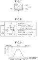
- the power transmitting resonant capacitor 116b which is the variable capacitor that uses the electromagnetic effect, etc., is disposed as illustrated in Fig. 7 .
- the power transmitting resonant capacitor 116b is disposed inward of looped wiring 312 wound around a core 310 of the power transmitting coil 112, on a surface of the core 310 that corresponds to the coil surface extending along the looped wiring 312.
- Z1 Z1r
- Z1n Z1r
- the third embodiment is obtained by applying, as the configuration described in the first embodiment in which the input impedance Z1 is changeable, a configuration in which a power transmitting coil 112c, which is a variable coil with variable inductance, is used as illustrated in Fig. 8 .
- the value of the inductance Lt of the power transmitting coil changes significantly depending on the positional relationship of the power receiving coil with respect to the power transmitting coil.
- Fig. 9 shows properties in which the inductance Lt in the fully facing position is the resonant inductance L1 satisfying the resonance condition, and as the coils are shifted from the fully facing state, the inductance Lt is reduced, and the inductance Lt in the non-facing state is significantly less than the resonant inductance L1.
- This property change is due to the following reason. Specifically, as illustrated in Fig.
- a portion of the magnetic flux generated from the power transmitting coil 112 passes through a magnetic body 211 of the power receiving coil 212 having high permeability, and thus the power transmitting coil 112 has high inductance.
- a portion of the magnetic flux generated from the power transmitting coil 112 passes through an air area having low permeability, and thus the power transmitting coil 112 has low inductance. Note that these properties are more prominent with a shorter distance (spacing) between the power transmitting coil and the power receiving coil and a greater coupling coefficient. Therefore, a coupling coefficient k in the fully facing state is preferably set to satisfy k ⁇ 0.1.
- the inductance Lt of the power transmitting coil 112c is set to a value significantly smaller than the resonant inductance L1 so as to place the power transmitting resonant circuit 110 out of the resonance state.
- both this configuration in which the inductance of the power transmitting coil is variable and the configuration according to the second embodiment in which the capacitance of the resonant capacitor is variable may be applied.
- the advantageous effects described in the first embodiment can be more effectively obtained.
- the fourth embodiment is obtained by applying, as the configuration described in the first embodiment in which the input impedance Z1 is changeable, a configuration in which a power transmitting resonant capacitor 116d, which is a variable capacitor with variable capacitance, is used as illustrated in Fig. 11 .
- a power transmitting resonant capacitor 116d which is a variable capacitor with variable capacitance
- the variable capacitor used as the power transmitting resonant capacitor 116b according to the second embodiment is a variable capacitor that uses the electromagnetic effect, etc.
- variable capacitor used as the power transmitting resonant capacitor 116d according to the fourth embodiment is a commonly used variable capacitor with the capacitance Ct that changes according to control input given thereto, that is, a control voltage Vc in the present example.
- the filter circuit 120 need not be provided.
- variable control circuit 320 which controls the capacitance Ct of the power transmitting resonant capacitor 116d is provided in the contactless power feeding device 100 according to the fourth embodiment.
- the variable control circuit 320 includes an electric current sensor 322, a rectifier circuit 324, a low-pass filter circuit 326 (hereinafter also referred to as a "LPF circuit 326"), and a voltage conversion circuit 328.
- LPF circuit 326 low-pass filter circuit 326
- the electric current sensor 322 detects an electric current flowing in one wire that connects the filter circuit 120 and the power transmitting resonant circuit 110, that is, an electric current flowing to the power transmitting coil 112, and outputs the detected electric current as a detected voltage. Note that the electric current sensor 322 may detect an electric current flowing in the other wire.
- the rectifier circuit 324 rectifies the detected voltage.
- the LPF circuit 326 removes a high-frequency component from the detected voltage.
- the voltage conversion circuit 328 converts the detected voltage into a control voltage Vc for controlling the capacitance Ct of the power transmitting resonant capacitor 116 according to the magnitude of the difference between the detected voltage and a reference voltage Vrc using a differential amplifier circuit.
- the electric current detected by the electric current sensor 322 is very small when the power receiving coil 212 is in the non-facing state with respect to the power transmitting coil 112, and increases as the state changes from the non-facing state to the facing state and further to the fully facing state. Therefore, the detected voltage from the electric current sensor 322 changes according to this change in the electric current.
- the capacitance Ct of the power transmitting resonant capacitor 116d is the resonant capacitance C1 in the fully facing state and is set to a capacitance Cnf less than the preset resonant capacitance C1 in the border state (refer to Fig. 2 ) which is the non-facing state.
- the voltage conversion circuit 328 is configured to receive the detected voltage by the negative input of the differential amplifier circuit so that the control voltage Vc to be output is reduced as the detected voltage from the electric current sensor 322 increases (refer to Fig. 11 ). Note that if the variable capacitor used as the power transmitting resonant capacitor 116d has the opposite properties, it is sufficient that the voltage conversion circuit 328 be configured to receive the detected voltage by the positive input of the differential amplifier circuit.
- the capacitance Cnf of the power transmitting resonant capacitor 116d is preferably set to the capacitance Ct corresponding to a predetermined electric current Inf in an electric current Ic detected by the electric current sensor 322, as illustrated on the left-hand side in Fig. 12 .
- the predetermined electric current Inf is preferably set from the perspective of reducing magnetic flux leakage, loss, etc., that are caused due to the electric current flowing to the power transmitting coil 112 in the non-facing state.
- the variable control circuit 320 is capable of controlling the capacitance Ct of the power transmitting resonant capacitor 116d, depending on whether and how the power receiving coil 212 and the power transmitting coil 112 face each other.
- the capacitance Ct of the power transmitting resonant capacitor 116d is preferably set so as to change linearly when the facing area in which the power receiving coil 212 faces the power transmitting coil 112 is reduced from the area in the fully facing area, which is largest, to the area in the border state, which is zero, as illustrated in Figs. 13 to 15 , for example.
- the input impedance Z1 can be gradually increased; thus, the occurrences of a surge current or a surge voltage in the electric current or the voltage that is applied to the power transmitting coil 112 due to a sharp increase in the impedance can be reduced.
- the change in the capacitance Ct is not limited to the properties illustrated in Figs. 13 to 15 ; it is sufficient that the capacitance Ct be set so as to change linearly when the facing area is reduced from the area in the fully facing area, which is largest, to the area in the border state, which is zero, and this change can take various shapes.
- the configuration according to the third embodiment in which the power transmitting coil is variable may be applied to the fourth embodiment.
- the advantageous effects described in the first embodiment can be more effectively obtained.
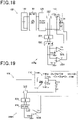
- the fifth embodiment is obtained by applying a configuration in which the power transmitting resonant capacitor 116d is used as with the configuration according to the fourth embodiment (refer to Fig. 10 ), as illustrated in Fig. 16 .
- the fifth embodiment is different from the fourth embodiment in that a variable control circuit 320e is included instead of the variable control circuit 320 according to the fourth embodiment.
- the variable control circuit 320e is the same as the variable control circuit 320 except that a magnetic field sensor 322e is included instead of the electric current sensor 322 in the variable control circuit 320. Note that the filter circuit 120 need not be provided.
- the magnetic field sensor 322e is disposed inward of the looped wiring 312 wound around the core 310 of the power transmitting coil 112, on a surface of the core 310 that corresponds to the coil surface extending along the looped wiring 312. This allows the magnetic field sensor 322e to detect a change in the magnetic flux that is generated by the power transmitting coil 112 depending on whether and how the power receiving coil 212 and the power transmitting coil 112 face each other, and output the detected voltage, as with the electric current sensor 322.
- variable control circuit 320e can also control the capacitance Ct of the power transmitting resonant capacitor 116d, depending on whether and how the power receiving coil 212 and the power transmitting coil 112 face each other.
- the configuration according to the third embodiment in which the power transmitting coil is variable may be applied to the fifth embodiment.
- the advantageous effects described in the first embodiment can be more effectively obtained.
- the sixth embodiment is obtained by applying, as the configuration described in the first embodiment in which the input impedance Z1 is changeable, a configuration in which a power transmitting coil 112f, which is a variable coil with variable inductance, is used as illustrated in Fig. 17 .
- the sixth embodiment is the same as the third embodiment in terms of using a variable coil as the power transmitting coil.
- the power transmitting coil 112c according to the third embodiment uses the properties in which the inductance changes depending on whether and how the power receiving coil and the power transmitting coil face each other.
- variable coil used as the power transmitting coil 112f according to the sixth embodiment is a variable coil with the inductance Lt that changes according to control input given thereto, that is, a control voltage V1 in the present example.
- variable coil various variable coils can be used such as a variable coil with inductance that changes when the number of turns of the coil is changed according to the control voltage VI, for example.
- the filter circuit 120 need not be provided.
- the contactless power feeding device 100 includes a variable control circuit 320f which controls the inductance Lt of the power transmitting coil 112f.
- the variable control circuit 320f is the same as the variable control circuit 320 according to the fourth embodiment (refer to Fig. 11 ).
- the reference voltage to be input to the voltage conversion circuit 328 and the control voltage to be output from the voltage conversion circuit 328, which are used to control the inductance Lt of the power transmitting coil 112f are referred to as a reference voltage Vrl and a control voltage VI, in order to distinguish from the reference voltage Vrc and the control voltage Vc in the variable control circuit 320.
- the variable control circuit 320f is capable of controlling the inductance Lt of the power transmitting coil 112f, depending on whether and how the power receiving coil 212 and the power transmitting coil 112 face each other.
- the advantageous effects described in the first embodiment can be obtained in the sixth embodiment as well.
- the value of the inductance Lt of the power transmitting coil 112 is changed to increase the input impedance Z1 in the non-facing state as described above, an increase in the size of the power transmitting coil 112 is problematic.
- the capacitance Ct of the power transmitting resonant capacitor 116 it is sufficient that the capacitance Ct of the power transmitting resonant capacitor 116 be reduced. Therefore, the value of the capacitance Ct of the power transmitting resonant capacitor 116 can be changed without causing an increase in the size of the power transmitting resonant capacitor 116.
- variable control circuit in which the electric current sensor 322 is used has thus far been described as an example of the variable control circuit 320f, but a variable control circuit in which the magnetic field sensor 322e is used as in the fifth embodiment can be applied.
- the seventh embodiment is obtained by applying both the configuration according to the fourth embodiment in which the power transmitting resonant capacitor 116d, which is a variable capacitor, is used (refer to Fig. 11 ) and the configuration according to the sixth embodiment in which the power transmitting coil 112f, which is a variable coil, is used (refer to Fig. 17 ), as illustrated in Fig. 18 .
- a variable control circuit 320g includes the electric current sensor 322, the rectifier circuit 324, the LPF circuit 326, and voltage conversion circuits 328c, 3281.
- the voltage conversion circuit 328c is the same as the voltage conversion circuit 328 according to the fourth embodiment that outputs the control voltage Vc for the power transmitting resonant capacitor 116d
- the voltage conversion circuit 3281 is the same as the voltage conversion circuit 328 according to the sixth embodiment that outputs the control voltage V1 for the power transmitting coil 112f. Note that the filter circuit 120 need not be provided.
- the variable control circuit 320g is capable of controlling the capacitance Ct of the power transmitting resonant capacitor 116d and the inductance Lt of the power transmitting coil 112f, depending on whether and how the power receiving coil 212 and the power transmitting coil 112 face each other.
- the advantageous effects described in the first embodiment can be more effectively obtained than in the fourth and sixth embodiments.
- variable control circuit in which the electric current sensor 322 is used has thus far been described as an example of the variable control circuit 320g, but a variable control circuit in which the magnetic field sensor 322e is used as in the fifth embodiment (refer to Fig. 15 ) can be applied.
- the eighth embodiment is obtained by applying, as the configuration described in the first embodiment in which the input impedance Z1 is changeable, a configuration in which a power transmitting resonant capacitor 116h with capacitance variable by turning ON and OFF a switch is used as illustrated in Fig. 19 .
- Fig. 19 illustrates only the power transmitting resonant circuit 110 among the structural elements of the contactless power feeding device 100 illustrated in Fig. 1 or 5 , together with a variable control circuit 320h which is used to change the value of the capacitance Ct of the power transmitting resonant capacitor 116h in the power transmitting resonant circuit 110, while the other structural elements are omitted therein.
- the power transmitting resonant capacitor 116h includes a first resonant capacitor 116ha and a second resonant capacitor 116hb arranged in parallel.
- the second resonant capacitor 116hb is connected in parallel with the first resonant capacitor 116ha when a bidirectional switch 117 connected in series with the second resonant capacitor 116hb is ON, and is disconnected when the bidirectional switch 117 is OFF.
- the capacitance Ct of the power transmitting resonant capacitor 116h is capacitance Chs of the first resonant capacitor 116ha when the bidirectional switch 117 is OFF, and is the sum of the capacitance Chs of the first resonant capacitor 116ha and capacitance Chl of the second resonant capacitor 116hb, that is, Chs + Ch1, when the bidirectional switch 117 is ON.
- the variable control circuit 320h is basically the same as the variable control circuit 320 (refer to Fig. 11 ) according to the fourth embodiment which includes the electric current sensor 322.
- the variable control circuit 320h may be substantially the same as the variable control circuit 320e (refer to Fig. 16 ) according to the fifth embodiment which includes the magnetic field sensor 322e.
- the voltage conversion circuit 328 which outputs the control voltage Vc corresponding to the magnitude of the difference between the detected voltage and the reference voltage Vrc is replaced by a voltage conversion circuit 328h in which a comparator that outputs a control voltage Vs corresponding to the magnitude relationship of a detected voltage Vd with respect to a threshold voltage Vth is used.
- the threshold voltage Vth is preferably set to a start threshold value Vth_on when the state changes from the non-facing state to the facing state and the bidirectional switch 117 is to be turned ON, and is set to a stop threshold value Vth_off when the state changes from the facing state to the non-facing state and the bidirectional switch 117 is to be turned OFF.
- the voltage conversion circuit 328h When the detected voltage Vd is less than the threshold voltage Vth in the non-facing state, the voltage conversion circuit 328h outputs a control voltage Vs that turns OFF the bidirectional switch 117, and when the detected voltage Vd is greater than the threshold voltage Vth in the facing state, the voltage conversion circuit 328h outputs a control voltage Vs that turns ON the bidirectional switch 117.
- the capacitance Ct of the power transmitting resonant capacitor 116h is the capacitance Chs of the first resonant capacitor 116ha in the non-facing state and is the sum of the capacitance Chs of the first resonant capacitor 116ha and the capacitance Chl of the second resonant capacitor 116hb in the facing state.
- the variable control circuit 320h is capable of changing the value of the capacitance Ct of the power transmitting resonant capacitor 116h according to whether the power receiving coil 212 and the power transmitting coil 112 are in the facing state or in the non-facing state. This allows the variable control circuit 320h to automatically control supplying of electric power from the contactless power feeding device 100 to the power receiving device 200, as illustrated in Fig. 20 .
- the variable control circuit 320h detects that the detected voltage Vd is greater than or equal to the start threshold value Vth_on which is the threshold voltage Vth and the state has changed from the non-facing state to the facing state (Step S10: YES)
- the supplying of electric power from the contactless power feeding device 100 to the power receiving device 200 can start.
- the variable control circuit 320h detects that the detected voltage Vd is less than or equal to the stop threshold value Vth_off which is the threshold voltage Vth and the state has changed from the facing state to the non-facing state (Step S30: YES)
- the supplying of electric power from the contactless power feeding device 100 to the power receiving device 200 can stop.
- Z1 Z1r
- Z1n Z1r
- Z1r Z1n > Z1r
- variable control circuit for switching the directional switch 117 can be replaced by not only the configuration in which the electric current sensor 322 illustrated in Fig. 19 is used or the configuration in which the magnetic field sensor 322e illustrated in Fig. 16 is used, but also the configuration in which a variable control circuit 320i illustrated in Fig. 21 or a variable control circuit 320j illustrated in Fig. 22 is used.
- the variable control circuit 320i includes a search coil 118 disposed facing the power transmitting coil 112.
- the variable control circuit 320i is configured to detect, as the detected voltage Vd, an alternating-current voltage generated between the terminals of the search coil 118 according to whether the power receiving coil 212 and the power transmitting coil 112 are in the facing state or in the non-facing state, and perform control to switch the bidirectional switch 117 by the control voltage Vs output according to the magnitude relationship of the detected voltage Vd with respect to the threshold voltage Vth.
- the variable control circuit 320j is configured to detect, as the detected voltage Vd, an alternating-current voltage generated between the terminals of the power transmitting coil 112 according to whether the power receiving coil 212 and the power transmitting coil 112 are in the facing state or in the non-facing state, and perform control to switch the bidirectional switch 117 by the control voltage Vs output according to the magnitude relationship of the detected voltage Vd with respect to the threshold voltage Vth.
- the ninth embodiment is obtained by applying a configuration in which a power transmitting resonant capacitor 116k is used instead of the power transmitting resonant capacitor 116h (refer to Fig. 19 ) according to the eighth embodiment, as illustrated in Fig. 23 .
- Fig. 23 illustrates only the power transmitting resonant circuit 110 among the structural elements of the contactless power feeding device 100, together with the variable control circuit 320h which is used to change the value of the capacitance Ct of the power transmitting resonant capacitor 116k in the power transmitting resonant circuit 110, while the other structural elements are omitted therein.
- the power transmitting resonant capacitor 116k includes a first resonant capacitor 116ka and a second resonant capacitor 116kb arranged in series.
- the first resonant capacitor 116ka is connected in series with the second resonant capacitor 116kb when the bidirectional switch 117 connected in parallel with the first resonant capacitor 116ka is OFF, and is short-circuited when the bidirectional switch 117 is ON. Therefore, when the variable control circuit 320h turns ON the bidirectional switch 117 in the facing state, the capacitance Ct of the power transmitting resonant capacitor 116k is the capacitance Chl of the second resonant capacitor 116kb.
- the capacitance Ct of the power transmitting resonant capacitor 116k is the sum (Chs ⁇ Chl / (Chs + Chl)) of the reciprocal of the capacitance Chs of the first resonant capacitor 116ka and the reciprocal of the capacitance Chl of the second resonant capacitor 116kb.
- the variable control circuit 320h is capable of changing the value of the capacitance Ct of the power transmitting resonant capacitor 116k according to whether or not the power receiving coil 212 and the power transmitting coil 112 are in the facing state or in the non-facing state. This allows the variable control circuit 320h to automatically control supplying of electric power from the contactless power feeding device 100 to the power receiving device 200, as illustrated in Fig. 20 .
- Z1 Z1r
- Z1n Z1r
- Z1r Z1n > Z1r
- variable control circuit according to the ninth embodiment may be a configuration substantially the same as the variable control circuit 320e (refer to Fig. 16 ) in which the magnetic field sensor 322e is used, instead of the configuration of the variable control circuit 320h or the like in which the electric current sensor 322 is used, as described in the eighth embodiment.
- the variable control circuit according to the ninth embodiment may be the variable control circuit 320i configured to use the search coil 118 as illustrated in Fig. 21 or the variable control circuit 320j illustrated in Fig. 22 and configured to detect a voltage between the terminals of the power transmitting coil 112.
- the power transmitting resonant circuit 110 in the contactless power feeding device 100 illustrated in Fig. 1 is a series resonant circuit including the power transmitting coil 112 and the power transmitting resonant capacitor 116 connected in series
- the power receiving resonant circuit 210 in the power receiving device 200 is also a series resonant circuit including the power receiving coil 212 and the power receiving resonant capacitor 216 connected in series.
- the power transmitting resonant circuit 110 in the contactless power feeding device 100 illustrated in Fig. 1 is a series resonant circuit including the power transmitting coil 112 and the power transmitting resonant capacitor 116 connected in series
- the power receiving resonant circuit 210 in the power receiving device 200 is also a series resonant circuit including the power receiving coil 212 and the power receiving resonant capacitor 216 connected in series.
- the power transmitting resonant circuit in the contactless power feeding device 100 may be a power transmitting resonant circuit 1101 which is a parallel resonant circuit including the power transmitting coil 112 and the power transmitting resonant capacitor 116 connected in parallel
- the power receiving resonant circuit in the power receiving device 200 may be a power receiving resonant circuit 2101 which is a parallel resonant circuit including the power receiving coil 212 and the power receiving resonant capacitor 216 connected in parallel.
- the capacitance Ct of the power transmitting resonant capacitor 116 and the inductance Lt of the power transmitting coil 112 are set so that the power transmitting resonant circuit 1101 resonates in parallel in the facing state in which the power receiving coil 212 faces the power transmitting coil 112.
- the power transmitting resonant circuit 1101 which is a parallel resonant circuit has greater advantageous effects than the power transmitting resonant circuit 110 which is a series resonant circuit, in terms of reducing the electric currents flowing from the power transmitting circuit, in other words, reducing the standby power consumption.
- the power transmitting resonant circuit 1101 which is a parallel resonant circuit a leakage current ILC flows between the power transmitting resonant capacitor 116 and the power transmitting coil 112, and thus a leakage magnetic field is generated at the power transmitting coil 112. Therefore, the power transmitting resonant circuit 1101 which is a parallel resonant circuit is less advantageous than the power transmitting resonant circuit 110 which is a series resonant circuit, in terms of reducing the leakage magnetic field.
- the eleventh embodiment is obtained by applying a power transmitting resonant circuit 110m and the power receiving resonant circuit 210 illustrated in Fig. 25 , in order to solve the problem of the leakage magnetic field in the power transmitting resonant circuit 1101 which is a parallel resonant circuit described in the tenth embodiment.
- the power transmitting resonant circuit 110m is a parallel-series resonant circuit including: a series capacitor 116s connected in series with the power transmitting coil 112; and a parallel capacitor 116p connected in parallel with the power transmitting coil 112 and the series capacitor 116s.
- the power receiving resonant circuit 210 is a series resonant circuit including the power receiving coil 212 and the power receiving resonant capacitor 216 connected in series.
- a resonance method based on primary parallel-series and secondary series capacitors (also referred to as the "PSS method") is applied to the power transmitting resonant circuit 110m and the power receiving resonant circuit 210.
- Capacitance Cpt of the parallel capacitor 116p in the power transmitting resonant circuit 110m, capacitance Cst of the series capacitor 116s in the power transmitting resonant circuit 110m, and the capacitance Cr of the power receiving resonant capacitor 216 in the power receiving resonant circuit 210 are set so that the power transmitting resonant circuit 110m resonates in parallel and the power receiving resonant circuit 210 resonates in series in the facing state in which the power transmitting coil 112 and the power receiving coil 212 face each other.
- these settings are configured using the following expressions (7) to (9).
- k is a coupling coefficient for the power transmitting coil 112 and the power receiving coil 212.
- the input impedance Z1 in the facing state in which the power transmitting coil 112 and the power receiving coil 212 face each other is represented by the following expression (10).
- Z 1 j ⁇ L 1 Lm 2 RL
- Lm is mutual inductance between the power transmitting coil 112 and the power receiving coil 212
- RL is a load equivalent to the power receiving circuit 220 and the battery 230.
- the input impedance Z1 of the power transmitting resonant circuit 110m becomes the input impedance represented by the above expression (10), an electric current flows from the power transmitting circuit to the power transmitting resonant circuit 110m, and thus electric power is supplied from the contactless power feeding device 100 to the power receiving device 200.
- the coupling coefficient k is reduced, and the mutual inductance Lm is reduced to approach zero. Accordingly, the value of the denominator in the above expression (10) is reduced toward zero, and thus the input impedance Z1 increases. As a result, the input electric current for the power transmitting resonant circuit 110m can be reduced, meaning that the electric currents from the power transmitting circuit can be reduced, in other words, the standby power consumption can be reduced.
- the capacitance Cst of the series capacitor 116s is preferably reduced from the value set according to the above expression (8). Accordingly, impedance Zs on the coil path side indicated in the following expression (11) can be increased, and thus the leakage current flowing to the power transmitting coil 112 can be reduced to reduce the generation of the leakage magnetic field.
- impedance Zs on the coil path side indicated in the following expression (11) can be increased, and thus the leakage current flowing to the power transmitting coil 112 can be reduced to reduce the generation of the leakage magnetic field.
- the capacitance Cp of the parallel capacitor 116p is preferably reduced from the value set according to the above expression (7). Accordingly, impedance Zp on the parallel capacitor path side indicated in the following expression (12) can further be increased, and thus the input electric current for the power transmitting resonant circuit 110m can further be reduced. As a result, the electric currents from the power transmitting circuit, in other words, the standby power consumption, can be more effectively reduced.
- the twelfth embodiment is obtained by applying a power transmitting resonant circuit 110n including a relay resonant circuit to the power transmitting resonant circuit 110 which is a series resonant circuit described in the first embodiment, as illustrated in Fig. 26 .
- the power transmitting resonant circuit 110n includes: a power transmitting resonant circuit portion including the power transmitting coil 112 and a power transmitting resonant capacitor 116n which are substantially the same as those in the power transmitting resonant circuit 110; and a relay resonant circuit portion including a relay coil 114 and a relay resonant capacitor 119 which form a closed loop circuit.
- the relay coil 114 is provided so as to satisfy the positional relationship having a predetermined coupling coefficient k1h with respect to the power transmitting coil 112.
- the capacitance Ct of the power transmitting resonant capacitor 116n in the power transmitting resonant circuit 110n, the capacitance Cht of the relay resonant capacitor 119 in the power transmitting resonant circuit 110n, and the capacitance Cr of power receiving resonant capacitor 216 in the power receiving resonant circuit 210 are set so that the power transmitting resonant circuit portion, the relay circuit portion, and the power receiving resonant circuit 210 resonate in the facing state in which the power transmitting coil 112 and the power receiving coil 212 face each other.
- these settings are configured using the following expressions (13) to (15).
- k1h is a coupling coefficient for the power transmitting coil 112 and the relay coil 114
- kh2 is a coupling coefficient for the relay coil 114 and the power receiving coil 212
- K12 is a coupling coefficient for the power transmitting coil 112 and the power receiving coil 212.
- RL is a load equivalent to the power receiving circuit 220 and the battery 230.
- the input impedance Z1 of the power transmitting resonant circuit 110n becomes the input impedance represented by the above expression (16), an electric current flows from the power transmitting circuit to the power transmitting resonant circuit 110n, and thus electric power is supplied from the contactless power feeding device 100 to the power receiving device 200.
- an electric current Iht flowing on the relay coil 114 side is represented by the following expression (17) in the non-facing state, and is represented by the following expression (18) when the power transmitting resonant circuit portion, the relay resonant circuit portion, and the power receiving resonant circuit 210 resonate in the facing state.
- Iht j ⁇ Lm j ⁇ L 1 ⁇ 1 ⁇ Ct j ⁇ Lht ⁇ 1 ⁇ Cht + ⁇ 2 L 1 h 2 V 1
- Iht 1 ⁇ L 1 h V 1
- Lm is mutual inductance between the power transmitting coil 112 and the power receiving coil 212
- L1h is mutual inductance between the power transmitting coil 112 and the relay coil 114
- V1 is an input voltage for the power transmitting resonant circuit 110m.
- the coupling coefficient kh2 is reduced to approach zero. Accordingly, the value of the denominator in the above expression (16) is reduced toward zero, and thus the input impedance Z1 increases. As a result, the input electric current for the power transmitting resonant circuit 110n can be reduced, meaning that the electric currents from the power transmitting circuit can be reduced, in other words, the standby power consumption can be reduced.
- the capacitance Ct of the power transmitting resonant capacitor 116n in the power transmitting resonant circuit portion is preferably reduced from the value set according to the above expression (13).
- the voltage to be applied to the power transmitting coil 112 can be reduced by further increasing the input impedance Z1.
- the capacitance Ct of the power transmitting resonant capacitor 116n is reduced, the denominator in the above expression (17) increases, allowing a reduction in the electric current Iht which flows to the relay coil 114 and allowing a reduction in the leakage magnetic field that is generated at the relay coil 114.
- the capacitance Cht of the relay resonant capacitor 119 may also be reduced from the value set according to the above expression (14). This also allows a reduction in the electric current Iht which flows to the relay coil 114.
- the input impedance Z1 of the power transmitting resonant circuit is changed according to whether and how the power receiving coil 212 and the power transmitting coil 112 face each other.
- the filter circuit 120 may be placed in the resonance state in the facing state and may be placed out of the resonance state in the non-facing state. Specifically, as illustrated in Fig.
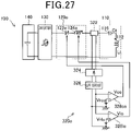
- a variable control circuit 320o may be used to provide the configuration in which the capacitance of a filter capacitor 122o included in a filter circuit 120o and the inductance of a filter coil 124o included in the filter circuit 120o are changeable.
- the filter circuit 120o is a band-pass filter circuit including the capacitor 122o and the coil 124o connected in series. The positioning of the capacitor 122o and the coil 124o may be opposite.
- the capacitor 122o is a variable capacitor with capacitance variable according to a control voltage Vco. As the variable capacitor, various commonly used variable capacitors can be applied.
- the coil 124o is a variable coil with inductance variable according to a control voltage Vlo. As the variable coil, various commonly used variable coils can be applied.
- variable control circuit 320h The configuration of the variable control circuit 320h is the same as that of the variable control circuit 320g except that voltage conversion circuits 328co, 3281o are included instead of the voltage conversion circuits 328c, 3281 in the variable control circuit 320g (refer to Fig. 18 ) according to the seventh embodiment.
- the voltage conversion circuit 328co is the same as the voltage conversion circuit 328c except that the control voltage Vco for controlling the capacitance of the capacitor 122o is output using a reference voltage Vrco as a reference.
- the voltage conversion circuit 3281o is the same as the voltage conversion circuit 3281 except that the control voltage Vlo for controlling the inductance of the coil 124o is output using a reference voltage Vrlo as a reference.
- the variable control circuit 320o is capable of controlling the inductance of the coil 124o in the filter circuit 120o and the capacitance of the capacitor 122o in the filter circuit 120o according to whether and how the power receiving coil 212 and the power transmitting coil 112 face each other. Specifically, in the non-facing state, the inductance and the capacitance are reduced, causing an increase in the input impedance for the filter circuit 120o and a reduction in the electric current that flows from the power transmitting circuit 130. In contrast, in the facing state, the inductance and the capacitance are increased so as to enable band-pass filter functions. Thus, advantageous effects substantially the same as the advantageous effects described in the first embodiment can be obtained in the thirteenth embodiment as well.
- variable control circuit in which the electric current sensor 322 is used has thus far been described as an example of the variable control circuit 320o, but a variable control circuit in which the magnetic field sensor 322e is used as in the fifth embodiment (refer to Fig. 15 ) can be applied.
- only one of the inductance of the coil 124o in the filter circuit 120o and the capacitance of the capacitor 122o in the filter circuit 120o is changed instead of changing both.
- not only is at least one of the inductance of the coil 124o in the filter circuit 120o and the capacitance of the capacitor 122o in the filter circuit 120o variable, but also at least one of the inductance of the power transmitting coil 112 in the power transmitting resonant circuit 110 and the capacitance of the power transmitting resonant capacitor 116 in the power transmitting resonant circuit 110 is variable.
- the filter capacitor may include two or more capacitors, and a configuration in which the capacitance of the filter capacitor is changeable may be applied by switching the connection of the two or more capacitors.
- the filter inductor may include two or more inductors, and a configuration in which the inductance of the filter inductor is changeable may be applied by switching the connection of the two or more inductors.
- the fourteenth embodiment is obtained by replacing the filter circuit 120o (refer to Fig. 27 ) according to the thirteenth embodiment and the variable control circuit 320o which controls the filter circuit 120o by a filter circuit 120p and a variable control circuit 320p which controls the filter circuit 120p, as illustrated in Fig. 28 .
- the filter circuit 120p is an immittance filter circuit including one filter capacitor 122p and two filter coils 124p, 124p.
- the capacitor 122p is a variable capacitor with capacitance variable according to a control voltage Vcp.
- As the variable capacitor various commonly used variable capacitors can be applied.
- the coil 124p is a variable coil with inductance variable according to a control voltage Vlp. As the variable coil, various commonly used variable coils can be applied.
- the variable control circuit 320p is the same as the variable control circuit 320o except that voltage conversion circuits 328cp, 3281p are included instead of the voltage conversion circuits 328co, 3281o in the variable control circuit 320o (refer to Fig. 27 ) according to the thirteenth embodiment.
- the voltage conversion circuit 328cp is the same as the voltage conversion circuit 328co except that the control voltage Vcp for controlling the capacitance of the capacitor 122p is output using a reference voltage Vrcp as a reference.
- the voltage conversion circuit 3281p is the same as the voltage conversion circuit 3281o except that the control voltage Vlp for controlling the inductance of the coil 124p is output using a reference voltage Vrlp as a reference.
- the variable control circuit 320p is capable of controlling the inductance of the coil 124p in the filter circuit 120p and the capacitance of the capacitor 122p in the filter circuit 120p according to whether and how the power receiving coil 212 and the power transmitting coil 112 face each other. Specifically, in the non-facing state, the inductance and the capacitance are reduced, causing an increase in the input impedance for the filter circuit 120p and a reduction in the electric current that flows from the power transmitting circuit 130. In contrast, in the facing state, the inductance and the capacitance are increased so as to enable immittance filter functions. Thus, advantageous effects substantially the same as the advantageous effects described in the first embodiment can be obtained in the fourteenth embodiment as well.
- variable control circuit in which the electric current sensor 322 is used has thus far been described as an example of the variable control circuit 320p, but a variable control circuit in which the magnetic field sensor 322e is used as in the fifth embodiment (refer to Fig. 15 ) can be applied.
- the configuration in which both the capacitance of the capacitor 122p and the inductance of the coil 124p are controlled has thus far been described as an example, but a configuration in which one of the capacitance of the capacitor 122p and the inductance of the coil 124p is controlled may also be applicable.
- a configuration in which one of the capacitance of the capacitor 122p and the inductance of the coil 124p is controlled may also be applicable.
- the filter capacitor may include two or more capacitors, and a configuration in which the capacitance of the filter capacitor is changeable may be applied by switching the connection of the two or more capacitors.
- the filter inductor may include two or more inductors, and a configuration in which the inductance of the filter inductor is changeable may be applied by switching the connection of the two or more inductors may be applied.
- the thirteenth embodiment describes an exemplary configuration in which a band-pass filter circuit is applied as the filter circuit and the fourteenth embodiment describes an exemplary configuration in which an immittance filter circuit is applied as the filter circuit, but these are not limiting; other various filter circuits can also be applied.
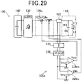
- the fifteenth embodiment is obtained by replacing the power transmitting resonant circuit 110 of the series resonance type (refer to Fig. 27 ) according to the thirteenth embodiment by the power transmitting resonant circuit 1101 of the parallel resonance type (refer to Fig. 24 ), as illustrated in Fig. 29 .
- the advantageous effects described in the first embodiment can also be obtained as in the thirteenth embodiment.
- the filter circuit 120o may be other filter circuits such as the filter circuit 120p (refer to Fig. 28 ) according to the fourteenth embodiment.
- the power transmitting resonant circuit may be replaced by the power transmitting resonant circuit 110m of the parallel resonance type illustrated in Fig. 25 .
- the contactless power feeding device 100 has thus far been described as including one power transmitting resonator as an example, but this is not limiting; the contactless power feeding device 100 may include two or more power transmitting resonators in parallel with one power transmitting circuit, as illustrated in Figs. 30 to 32 .
- Fig. 30 illustrates a configuration in which two or more power transmitting resonant circuits 110 each of which is illustrated in Fig. 1 are arranged in parallel with the power transmitting circuit 130 as the power transmitting resonator.
- Fig. 31 illustrates a configuration in which one filter circuit 120 is disposed between the power transmitting circuit 130 and the two or more power transmitting resonant circuits 110.
- the power transmitting resonant circuit 110 including the power transmitting coil 112 which the power receiving coil 212 in the power receiving resonant circuit 210 of the power receiving device 200 faces operate in substantially the same manner as in the facing state described in the first embodiment, and the other power transmitting resonant circuits 110 operate in substantially the same manner as in the non-facing state described in the first embodiment.
- advantageous effects substantially the same as the advantageous effects described in the first embodiment can be obtained.
- Fig. 32 illustrates a configuration in which two or more sets of the filter circuit 120 and the power transmitting resonant circuit 110 illustrated in Fig. 5 are arranged in parallel with the power transmitting circuit 130 as the power transmitting resonator.
- the power transmitting resonant circuit 110 including the power transmitting coil 112 which the power receiving coil 212 in the power receiving resonant circuit 210 of the power receiving device 200 faces operate in substantially the same manner as in the facing state described in the first embodiment, and the other power transmitting resonant circuits 110 operate in substantially the same manner as in the non-facing state described in the first embodiment.
- the filter circuit 120 including the power transmitting coil 112 which the power receiving coil 212 in the power receiving resonant circuit 210 of the power receiving device 200 faces operate in substantially the same manner as with the filter circuit (refer to Figs. 27 and 28 ) in the facing state described in the thirteenth and fourteenth embodiments, and the other filter circuits 120 operate in substantially the same manner as with the filter circuit in the non-facing state described in the thirteenth and fourteenth embodiments.
- advantageous effects substantially the same as the advantageous effects described in the thirteenth and fourteenth embodiments and the first embodiment can be obtained.
- the power transmitting resonant circuits illustrated in Figs. 1 and 5 are cited as examples for the contactless power feeding devices including the plurality of power transmitting resonators illustrated in Figs. 30 to 32 , but the power transmitting resonant circuit portion described in other embodiments can also be applied.
- the contactless power feeding device including the plurality of power transmitting resonators illustrated in Fig. 32 includes the filter circuits illustrated in Figs. 27 and 28 as an example, but may include other filter circuits as an example.
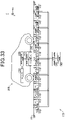
- the contactless power feeding devices 100 including the plurality of power feeding resonators illustrated in Figs. 30 to 32 can be applied as contactless power feeding devices in contactless power feeding systems for vehicles, as illustrated in Figs. 33 to 35 .
- the contactless power feeding systems for vehicles illustrated in Figs. 33 to 35 are power feeding systems capable of supplying electric power from the contactless power feeding device 100 installed along the course of a vehicle travel path RS to a vehicle (hereinafter also referred to as a "vehicle 200") that is the power receiving device 200.
- the vehicle 200 is configured as an electric vehicle or a hybrid vehicle, for example.
- the x-axis direction indicates a direction of travel of the vehicle 200 along the lane of the vehicle travel path RS
- the y-axis direction indicates the width direction of the vehicle travel path RS
- the z-axis direction indicates the upward vertical direction.
- the directions of the x, y, and z axes in the other figures to be described later indicate the same directions as those in Figs. 33 to 35 .
- the power transmitting resonant circuit 110 includes: the power transmitting coil 112 installed in the vehicle travel path RS; and the power transmitting resonant capacitor 116 not illustrated in the drawings (refer to Figs. 30 to 32 ).
- the power transmitting coil 112 in each power transmitting resonant circuit 110 is aligned in the x direction along the lane of the vehicle travel path RS.
- Figs. 33 to 35 illustrate seven power transmitting resonant circuits 110. However, this is not limiting; two or more power transmitting coils 112 may be aligned in the x and y directions.
- the power receiving resonant circuit 210 includes the power receiving coil 212 and the power receiving resonant capacitor 216 not illustrated in the drawings (refer to Figs. 30 to 32 ), and at least the power receiving coil 212 is disposed at the bottom of the vehicle 200 so as to face the power transmitting coil 112 in the power transmitting resonant circuit 110.
- the alternating-current power obtained by the power receiving resonant circuit 210 is converted by the power receiving circuit 220 into direct-current power, and the direct-current power is used to charge the battery 230 and is used as energy for driving a motor or the like not illustrated in the drawings.
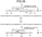
- the dimensions of the power transmitting coil 112 installed in the vehicle travel path RS are preferably set as described below.
- Fig. 36 illustrates settings in which electric power is supplied to the power receiving coil from all the power transmitting coils (the power transmitting coils indicated by hatching) each including a portion that faces the power receiving coil.
- a power transmitting coil dimension DTx in the direction of alignment of the power transmitting coils 112, that is, in the x direction is larger than or equal to a power receiving coil dimension DRx of the power receiving coil in the x direction
- the non-facing area can be smaller and the magnetic flux leakage can be less than those in the case of the top stage.
- Fig. 37 illustrates settings in which electric power is supplied to the power receiving coil from only the power transmitting coil (the power transmitting coil indicated by hatching) with at least 50% facing area between the power receiving coil and the power transmitting coil.
- the power transmitting coil dimension DTx is larger than or equal to the power receiving coil dimension DRx
- the non-facing area is large and the magnetic flux leakage is great, similar to the case illustrated in Fig. 36 .
- the area (facing area) of a portion of the power receiving coil 212 that faces the power transmitting coil 112 is small and the amount of electric power that can be received by the power receiving coil 212 is small.
- the non-facing area can be smaller and the magnetic flux leakage can be less than those in the case of the top stage.
- the facing area can be larger and the amount of electric power that can be received by the power receiving coil 212 can be larger than those in the case of the top stage.
- the dimensions of the power transmitting coil 112 are preferably set so that the power transmitting coil dimension DTx is smaller than the power receiving coil dimension DRx.
- the controllers and the methods used by the controllers that are described in the present disclosure may be implemented using a dedicated computer provided by configuring memory and a processor programmed by a computer program so as to perform one or more specific functions.
- the controllers and the methods used by the controllers that are described in the present disclosure may be implemented using a dedicated computer provided by configuring a processor with one or more dedicated hardware logic circuits.
- the controllers and the methods used by the controllers that are described in the present disclosure may be implemented using one or more dedicated computers including a combination of: memory and a processor programmed so as to perform one or more functions; and a processor configured with one or more hardware logic circuits.
- the computer program may be stored in a tangible nontransitory computer-readable recording medium as an instruction to be performed by a computer.
Landscapes
- Engineering & Computer Science (AREA)
- Computer Networks & Wireless Communication (AREA)
- Power Engineering (AREA)
- Charge And Discharge Circuits For Batteries Or The Like (AREA)
- Electric Propulsion And Braking For Vehicles (AREA)
- Current-Collector Devices For Electrically Propelled Vehicles (AREA)
Applications Claiming Priority (3)
| Application Number | Priority Date | Filing Date | Title |
|---|---|---|---|
| JP2019136680 | 2019-07-25 | ||
| JP2020087198A JP7163940B2 (ja) | 2019-07-25 | 2020-05-19 | 非接触給電装置 |
| PCT/JP2020/026128 WO2021014932A1 (ja) | 2019-07-25 | 2020-07-03 | 非接触給電装置 |
Publications (2)
| Publication Number | Publication Date |
|---|---|
| EP4007119A1 true EP4007119A1 (de) | 2022-06-01 |
| EP4007119A4 EP4007119A4 (de) | 2022-09-14 |
Family
ID=74193793
Family Applications (1)
| Application Number | Title | Priority Date | Filing Date |
|---|---|---|---|
| EP20844318.4A Pending EP4007119A4 (de) | 2019-07-25 | 2020-07-03 | Vorrichtung zur kontaktlosen stromversorgung |
Country Status (5)
| Country | Link |
|---|---|
| US (3) | US20220149664A1 (de) |
| EP (1) | EP4007119A4 (de) |
| JP (2) | JP7420191B2 (de) |
| CN (1) | CN114144959B (de) |
| WO (1) | WO2021014932A1 (de) |
Cited By (1)
| Publication number | Priority date | Publication date | Assignee | Title |
|---|---|---|---|---|
| EP4349635A4 (de) * | 2021-05-31 | 2024-12-25 | Denso Corporation | Stromversorgungssystem |
Families Citing this family (3)
| Publication number | Priority date | Publication date | Assignee | Title |
|---|---|---|---|---|
| WO2022254954A1 (ja) * | 2021-05-31 | 2022-12-08 | 株式会社デンソー | 給電システム |
| JP7718436B2 (ja) * | 2023-02-02 | 2025-08-05 | 株式会社デンソー | 可変容量コンデンサおよび給電装置 |
| JP7790368B2 (ja) * | 2023-02-02 | 2025-12-23 | 株式会社デンソー | 給電装置 |
Family Cites Families (39)
| Publication number | Priority date | Publication date | Assignee | Title |
|---|---|---|---|---|
| JP2000148932A (ja) * | 1998-11-13 | 2000-05-30 | Hitachi Ltd | リーダまたは/およびライタ装置およびそれを用いたicカードシステム |
| US9744858B2 (en) * | 2008-09-27 | 2017-08-29 | Witricity Corporation | System for wireless energy distribution in a vehicle |
| JP2011050140A (ja) * | 2009-08-26 | 2011-03-10 | Sony Corp | 非接触給電装置、非接触受電装置、非接触給電方法、非接触受電方法および非接触給電システム |
| US8374545B2 (en) * | 2009-09-02 | 2013-02-12 | Qualcomm Incorporated | De-tuning in wireless power reception |
| JP5537981B2 (ja) * | 2010-02-15 | 2014-07-02 | 株式会社豊田中央研究所 | 移動体給電装置 |
| JP5640530B2 (ja) * | 2010-07-30 | 2014-12-17 | ソニー株式会社 | ワイヤレス給電システム |
| KR101228557B1 (ko) * | 2010-11-30 | 2013-01-31 | 유한회사 한림포스텍 | 근거리 무선 전력 통신용 코일 공진 커플러 및 이를 포함하는 근거리 무선 전력 전송 장치 |
| KR101842180B1 (ko) * | 2010-12-24 | 2018-03-26 | 가부시키가이샤 한도오따이 에네루기 켄큐쇼 | 급전 장치 및 급전 장치를 구비한 비접촉 급전 시스템 |
| CN103370849B (zh) * | 2011-02-15 | 2017-03-22 | 丰田自动车株式会社 | 非接触受电装置及搭载有该装置的车辆、非接触供电设备、非接触受电装置的控制方法以及非接触供电设备的控制方法 |
| WO2012169015A1 (ja) * | 2011-06-07 | 2012-12-13 | パイオニア株式会社 | インピーダンス整合装置、制御方法 |
| JP5712289B2 (ja) * | 2011-06-07 | 2015-05-07 | パイオニア株式会社 | インピーダンス整合装置、制御方法 |
| JP2013021886A (ja) * | 2011-07-14 | 2013-01-31 | Sony Corp | 給電装置、給電システム、車両および電子機器 |
| JP2013078171A (ja) * | 2011-09-29 | 2013-04-25 | Semiconductor Energy Lab Co Ltd | 受電装置及び非接触給電システム |
| US9721721B2 (en) * | 2011-09-29 | 2017-08-01 | Lg Innotek Co., Ltd. | Wireless power transmitter, wireless power receiver and impedence control method |
| US9502920B2 (en) * | 2011-11-16 | 2016-11-22 | Semiconductor Energy Laboratory Co., Ltd. | Power receiving device, power transmission device, and power feeding system |
| JP6016596B2 (ja) * | 2011-12-07 | 2016-10-26 | 株式会社半導体エネルギー研究所 | 非接触給電システム |
| WO2013112609A1 (en) * | 2012-01-23 | 2013-08-01 | Utah State University | Switch wear leveling |
| CN104508945B (zh) * | 2012-07-30 | 2016-09-07 | 日产自动车株式会社 | 非接触供电装置 |
| CN106961164A (zh) * | 2012-10-11 | 2017-07-18 | 株式会社村田制作所 | 无线供电装置 |
| KR102028059B1 (ko) * | 2012-12-27 | 2019-10-04 | 삼성전자주식회사 | 무선 전력 전송 시스템의 공진 장치 및 방법 |
| US20150372500A1 (en) * | 2013-02-13 | 2015-12-24 | North Carolina State University | Systems and methods for wireless power transfer |
| GB2526444C (en) * | 2013-02-15 | 2020-09-23 | Murata Manufacturing Co | Wireless power supply apparatus |
| JP6178107B2 (ja) * | 2013-04-30 | 2017-08-09 | 矢崎総業株式会社 | 給電システム及び共振回路 |
| JP2015065756A (ja) * | 2013-09-25 | 2015-04-09 | 株式会社日本自動車部品総合研究所 | 受電装置および送電装置 |
| JP2015146722A (ja) * | 2014-01-06 | 2015-08-13 | 日東電工株式会社 | 無線電力伝送装置 |
| JP6146333B2 (ja) * | 2014-02-13 | 2017-06-14 | 株式会社豊田自動織機 | 送電機器及び非接触電力伝送装置 |
| JP6332002B2 (ja) * | 2014-11-01 | 2018-05-30 | パナソニックIpマネジメント株式会社 | 送電装置、送電装置を搭載した車両及び無線電力伝送システム |
| CN204442024U (zh) * | 2015-01-13 | 2015-07-01 | 华南理工大学 | 频率自优化动态调谐的磁耦合谐振无线输电装置 |
| CN108141055B (zh) * | 2015-04-30 | 2022-01-14 | 香港大学 | 在不使用互耦信息或者无线反馈的情况下的无线电能传输系统的发送器侧控制 |
| JP6460405B2 (ja) * | 2015-06-05 | 2019-01-30 | 株式会社デンソー | 非接触給電装置 |
| WO2017042904A1 (ja) * | 2015-09-09 | 2017-03-16 | 株式会社 東芝 | 無線電力伝送システム、送電装置および受電装置 |
| CN109075613B (zh) * | 2016-02-02 | 2022-05-31 | 韦特里西提公司 | 控制无线电力传输系统 |
| US10951066B2 (en) * | 2016-09-15 | 2021-03-16 | Nec Corporation | Wireless power supply device and wireless power supply method |
| JP6370484B1 (ja) * | 2017-03-10 | 2018-08-08 | 三菱電機エンジニアリング株式会社 | 共振型電力送信装置及び共振型電力伝送システム |
| JP2019071719A (ja) | 2017-10-07 | 2019-05-09 | 株式会社ワィティー | 移動体用ワイヤレス給電システム |
| WO2019201444A1 (en) * | 2018-04-19 | 2019-10-24 | Abb Schweiz Ag | A power transfer system for electric vehicles |
| EP3784517B1 (de) * | 2018-04-23 | 2023-02-15 | ABB E-mobility B.V. | Energieübertragungssystem für elektrofahrzeuge und steuerverfahren dafür |
| EP3802194B1 (de) * | 2018-05-24 | 2025-04-30 | ABB E-mobility B.V. | Verfahren zur kupplung von elektrischen fahrzeugen und stromanschlüssen in einer ladestation für elektrische fahrzeuge |
| GB201820840D0 (en) * | 2018-12-20 | 2019-02-06 | Metaboards Ltd | Load localisation |
-
2020
- 2020-07-03 WO PCT/JP2020/026128 patent/WO2021014932A1/ja not_active Ceased
- 2020-07-03 EP EP20844318.4A patent/EP4007119A4/de active Pending
- 2020-07-03 CN CN202080053312.2A patent/CN114144959B/zh active Active
-
2022
- 2022-01-25 US US17/583,822 patent/US20220149664A1/en not_active Abandoned
- 2022-10-06 JP JP2022161337A patent/JP7420191B2/ja active Active
- 2022-10-06 JP JP2022161338A patent/JP7420192B2/ja active Active
-
2025
- 2025-03-31 US US19/095,355 patent/US20250233458A1/en active Pending
- 2025-03-31 US US19/095,334 patent/US20250233457A1/en active Pending
Cited By (1)
| Publication number | Priority date | Publication date | Assignee | Title |
|---|---|---|---|---|
| EP4349635A4 (de) * | 2021-05-31 | 2024-12-25 | Denso Corporation | Stromversorgungssystem |
Also Published As
| Publication number | Publication date |
|---|---|
| EP4007119A4 (de) | 2022-09-14 |
| US20250233458A1 (en) | 2025-07-17 |
| US20220149664A1 (en) | 2022-05-12 |
| JP2022176341A (ja) | 2022-11-25 |
| US20250233457A1 (en) | 2025-07-17 |
| JP7420192B2 (ja) | 2024-01-23 |
| JP2022176340A (ja) | 2022-11-25 |
| JP7420191B2 (ja) | 2024-01-23 |
| WO2021014932A1 (ja) | 2021-01-28 |
| CN114144959A (zh) | 2022-03-04 |
| CN114144959B (zh) | 2025-01-07 |
Similar Documents
| Publication | Publication Date | Title |
|---|---|---|
| JP7163940B2 (ja) | 非接触給電装置 | |
| US20250233457A1 (en) | Contactless power feeding device | |
| EP2773019B1 (de) | Kontaktfreie energieempfangsvorrichtung | |
| CN104620465B (zh) | 车辆和非接触式供电系统 | |
| CN104620470B (zh) | 非接触供电系统以及在该系统中使用的送电装置和车辆 | |
| EP3631945B1 (de) | Steuerung eines multi-mode leistungsempfängers für drahtlos übertragene energie | |
| KR20140067134A (ko) | 비접촉 송전 장치, 비접촉 수전 장치 및 비접촉 송수전 시스템 | |
| US10076966B2 (en) | Contactless power transmission device, contactless power reception device, and contactless power transmission system | |
| Bhattacharya et al. | Design of static wireless charging coils for integration into electric vehicle | |
| US20150061402A1 (en) | Power reception device, power transmission device and power transfer system | |
| JP2013027129A (ja) | 給電側設備及び共鳴型非接触給電システム | |
| US20160001669A1 (en) | Vehicle And Contactless Power Feeding System | |
| EP3282556B1 (de) | Kontaktloses stromzufuhrsystem | |
| JP2014155278A (ja) | 変換ユニット | |
| US20230110224A1 (en) | Contactless power supply system and coil unit thereof | |
| US11901741B2 (en) | Wireless power transfer system | |
| JP6974244B2 (ja) | 非接触送電装置 |
Legal Events
| Date | Code | Title | Description |
|---|---|---|---|
| STAA | Information on the status of an ep patent application or granted ep patent |
Free format text: STATUS: THE INTERNATIONAL PUBLICATION HAS BEEN MADE |
|
| PUAI | Public reference made under article 153(3) epc to a published international application that has entered the european phase |
Free format text: ORIGINAL CODE: 0009012 |
|
| STAA | Information on the status of an ep patent application or granted ep patent |
Free format text: STATUS: REQUEST FOR EXAMINATION WAS MADE |
|
| 17P | Request for examination filed |
Effective date: 20220204 |
|
| AK | Designated contracting states |
Kind code of ref document: A1 Designated state(s): AL AT BE BG CH CY CZ DE DK EE ES FI FR GB GR HR HU IE IS IT LI LT LU LV MC MK MT NL NO PL PT RO RS SE SI SK SM TR |
|
| STAA | Information on the status of an ep patent application or granted ep patent |
Free format text: STATUS: EXAMINATION IS IN PROGRESS |
|
| A4 | Supplementary search report drawn up and despatched |
Effective date: 20220811 |
|
| RIC1 | Information provided on ipc code assigned before grant |
Ipc: H02J 50/40 20160101ALN20220805BHEP Ipc: H02J 50/50 20160101ALI20220805BHEP Ipc: H02J 50/90 20160101ALI20220805BHEP Ipc: H02J 50/12 20160101AFI20220805BHEP |
|
| 17Q | First examination report despatched |
Effective date: 20220823 |
|
| DAV | Request for validation of the european patent (deleted) | ||
| DAX | Request for extension of the european patent (deleted) |