EP4007148A1 - Procédé de démarrage d'un convertisseur à double pont actif pour empêcher les défaillances dues à la surtension et l'emballement thermique - Google Patents
Procédé de démarrage d'un convertisseur à double pont actif pour empêcher les défaillances dues à la surtension et l'emballement thermique Download PDFInfo
- Publication number
- EP4007148A1 EP4007148A1 EP21199151.8A EP21199151A EP4007148A1 EP 4007148 A1 EP4007148 A1 EP 4007148A1 EP 21199151 A EP21199151 A EP 21199151A EP 4007148 A1 EP4007148 A1 EP 4007148A1
- Authority
- EP
- European Patent Office
- Prior art keywords
- converter
- primary
- phase
- alternating current
- startup
- Prior art date
- Legal status (The legal status is an assumption and is not a legal conclusion. Google has not performed a legal analysis and makes no representation as to the accuracy of the status listed.)
- Granted
Links
Images







Classifications
-
- H—ELECTRICITY
- H02—GENERATION; CONVERSION OR DISTRIBUTION OF ELECTRIC POWER
- H02M—APPARATUS FOR CONVERSION BETWEEN AC AND AC, BETWEEN AC AND DC, OR BETWEEN DC AND DC, AND FOR USE WITH MAINS OR SIMILAR POWER SUPPLY SYSTEMS; CONVERSION OF DC OR AC INPUT POWER INTO SURGE OUTPUT POWER; CONTROL OR REGULATION THEREOF
- H02M3/00—Conversion of DC power input into DC power output
- H02M3/22—Conversion of DC power input into DC power output with intermediate conversion into AC
- H02M3/24—Conversion of DC power input into DC power output with intermediate conversion into AC by static converters
- H02M3/28—Conversion of DC power input into DC power output with intermediate conversion into AC by static converters using discharge tubes with control electrode or semiconductor devices with control electrode to produce the intermediate AC
- H02M3/325—Conversion of DC power input into DC power output with intermediate conversion into AC by static converters using discharge tubes with control electrode or semiconductor devices with control electrode to produce the intermediate AC using devices of a triode or a transistor type requiring continuous application of a control signal
- H02M3/335—Conversion of DC power input into DC power output with intermediate conversion into AC by static converters using discharge tubes with control electrode or semiconductor devices with control electrode to produce the intermediate AC using devices of a triode or a transistor type requiring continuous application of a control signal using semiconductor devices only
- H02M3/33569—Conversion of DC power input into DC power output with intermediate conversion into AC by static converters using discharge tubes with control electrode or semiconductor devices with control electrode to produce the intermediate AC using devices of a triode or a transistor type requiring continuous application of a control signal using semiconductor devices only having several active switching elements
- H02M3/33576—Conversion of DC power input into DC power output with intermediate conversion into AC by static converters using discharge tubes with control electrode or semiconductor devices with control electrode to produce the intermediate AC using devices of a triode or a transistor type requiring continuous application of a control signal using semiconductor devices only having several active switching elements having at least one active switching element at the secondary side of an isolation transformer
- H02M3/33584—Bidirectional converters
-
- H—ELECTRICITY
- H02—GENERATION; CONVERSION OR DISTRIBUTION OF ELECTRIC POWER
- H02M—APPARATUS FOR CONVERSION BETWEEN AC AND AC, BETWEEN AC AND DC, OR BETWEEN DC AND DC, AND FOR USE WITH MAINS OR SIMILAR POWER SUPPLY SYSTEMS; CONVERSION OF DC OR AC INPUT POWER INTO SURGE OUTPUT POWER; CONTROL OR REGULATION THEREOF
- H02M1/00—Details of apparatus for conversion
- H02M1/36—Means for starting or stopping converters
-
- H—ELECTRICITY
- H02—GENERATION; CONVERSION OR DISTRIBUTION OF ELECTRIC POWER
- H02M—APPARATUS FOR CONVERSION BETWEEN AC AND AC, BETWEEN AC AND DC, OR BETWEEN DC AND DC, AND FOR USE WITH MAINS OR SIMILAR POWER SUPPLY SYSTEMS; CONVERSION OF DC OR AC INPUT POWER INTO SURGE OUTPUT POWER; CONTROL OR REGULATION THEREOF
- H02M1/00—Details of apparatus for conversion
- H02M1/32—Means for protecting converters other than automatic disconnection
-
- H—ELECTRICITY
- H02—GENERATION; CONVERSION OR DISTRIBUTION OF ELECTRIC POWER
- H02M—APPARATUS FOR CONVERSION BETWEEN AC AND AC, BETWEEN AC AND DC, OR BETWEEN DC AND DC, AND FOR USE WITH MAINS OR SIMILAR POWER SUPPLY SYSTEMS; CONVERSION OF DC OR AC INPUT POWER INTO SURGE OUTPUT POWER; CONTROL OR REGULATION THEREOF
- H02M3/00—Conversion of DC power input into DC power output
- H02M3/22—Conversion of DC power input into DC power output with intermediate conversion into AC
- H02M3/24—Conversion of DC power input into DC power output with intermediate conversion into AC by static converters
- H02M3/28—Conversion of DC power input into DC power output with intermediate conversion into AC by static converters using discharge tubes with control electrode or semiconductor devices with control electrode to produce the intermediate AC
- H02M3/325—Conversion of DC power input into DC power output with intermediate conversion into AC by static converters using discharge tubes with control electrode or semiconductor devices with control electrode to produce the intermediate AC using devices of a triode or a transistor type requiring continuous application of a control signal
- H02M3/335—Conversion of DC power input into DC power output with intermediate conversion into AC by static converters using discharge tubes with control electrode or semiconductor devices with control electrode to produce the intermediate AC using devices of a triode or a transistor type requiring continuous application of a control signal using semiconductor devices only
- H02M3/33569—Conversion of DC power input into DC power output with intermediate conversion into AC by static converters using discharge tubes with control electrode or semiconductor devices with control electrode to produce the intermediate AC using devices of a triode or a transistor type requiring continuous application of a control signal using semiconductor devices only having several active switching elements
- H02M3/33573—Full-bridge at primary side of an isolation transformer
Definitions
- the present invention relates to power converters. More specifically, the invention relates to a system and method for controlling a dual active bridge (DAB) based DC/DC converter.
- DAB dual active bridge
- a DAB converter is a high-efficiency, high-power converter that comprises a primary converter coupled to a secondary converter by a high-frequency transformer, where each converter comprises a plurality of active power switching devices.
- a controller managing a phase shift between the primary and secondary converters controls the amount and direction of power flow.
- Three-phase and single-phase DAB based DC/DC converters can be used to realize touchsafe DC power from a high-voltage DC source in a variety of applications, including in a traction inverter used in a heavy-duty off-road vehicle.
- Startup of the DAB converter must be carried out by issuing switching commands to devices on the primary-side converter (i.e. the high-voltage source side) and followed by switching commands issued to the secondary-side converter. If not carefully started, the secondary-side converter in a DAB converter not only experiences current in-rush, which is a magnitude order higher than the secondary converter's nominal input current, but also the DC bus of the secondary converter charges up to ⁇ 1.3x nominal output voltage. Due to this excessive charge across the DC bus of the secondary converter, some of devices in the secondary converter can fail before a protection system is enacted.
- the voltage control bandwidth for a closed-loop DC voltage control is often set to a high value in order to achieve fast dynamics. Due to the high voltage control bandwidth, the phase-shift angle will have a large change during startup. The large phase-shift will require rapid flow of power from the primary converter to the secondary converter, which could further result in current in-rush experienced by the output capacitor, resulting in an excessive high peak value of current flowing at the input of the secondary converter. The current in-rush can trigger the gate drive de-sat faults in the secondary converter and often this current in-rush will instantly damage some of power devices in the secondary converter. It would therefore be advantageous to develop a control process to reduce the risk of damage to the DAB converter during startup.
- the process comprises a multi-step approach: pre-charge control and startup control.
- the pre-charge step increases the dead time of the pulse-width modulated signal to reduce the duty cycle, leading to a reduction in the DC bus capacitor current during startup.
- control bandwidth is limited by slewing the gains of a proportional-integral controller during the startup, preventing large changes in the phase-shift angle.
- a controller implementing the startup routine is also disclosed.
- the present invention provides a system and method as claimed.
- a three-phase dual active bridge based (DAB3) DC/DC converter 100 is shown in Fig. 1 .
- the DAB3 converter 100 has a primary converter 110 and a secondary converter 120 with alternating current (AC) outputs 111/121 of both converters 110/120 connected via an isolation transformer 130 with a turn ratio of N:1.
- the primary converter 110 and the secondary converter 120 may be coupled by a transformer 130 and one or more inductors 131.
- the DAB3 converter 100 includes a primary converter 110 comprising a plurality of power devices (or switches) 201, 202, 203, 204, 205, and 206 and a secondary converter 120 comprising a plurality of power devices 207, 208, 209, 210, 211, and 212.
- a pair of devices i.e. 201/202, 203/204, and 205/206) with each of phase A, phase B, and phase C.
- the power devices 201-212 may comprise an insulated gate bipolar transistor, a metal oxide semiconductor field effect transistor, a silicon carbide field effect transistor, or a similar semiconductor device.
- the power switching devices 201-206 are coupled between direct current terminals 112 of the primary converter 110 and the secondary switches 207-212 are coupled between direct current terminals 122 of the secondary converter 120.
- a primary winding 133 of the transformer 130 is coupled to output terminals of the primary power devices 201-206, whereas a secondary winding 134 of the transformer 130 is coupled to output terminals of the secondary power devices 207-212.
- the primary winding 133 of the transformer 130 is coupled to the primary AC terminal 111 and is associated with a primary alternating current signal of the primary converter 110; similarly, the secondary winding 134 of the transformer 130 is coupled to the secondary AC terminal 121 and is associated with a secondary alternating current signal of the secondary converter 120.
- Fig. 2 shows a single-phase dual active bridge based (DAB1) DC/DC converter 100.
- the DAB1 converter 100 has a similar topology to the DAB3 converter 100, but with differences attributed to single-phase use.
- the DAB1 converter 100 includes a primary converter 110 comprising a plurality of power devices 201, 202, 203, and 204 and a secondary converter 120 comprising a plurality of power devices 205, 206, 207, and 208.
- Like reference numbers indicate like features or elements.
- a control system or controller 140 for the DAB3 converter 100 is shown in Fig. 3 .
- a similar controller 140 can be used for the DAB1 converter 100.
- the control system 140 may include an electronic data processor 141 comprising one or more of: a field programmable gate array (FPGA), a microprocessor, a microcontroller, a programmable logic device, an arithmetic logic unit, a Boolean logic unit, an electronic circuit or system, a digital circuit, a digital signal processor (DSP), an application specific integrated circuit (ASIC), or another data processing device.
- the electronic data processor 141 can execute software instructions.
- the control system 140 is adapted to implement a scheme to realize phase-shifted pulse width modulated (PWM) switching signals for the primary converter devices 201-206 and secondary converter devices 207-212. As shown in Fig. 3 , in one embodiment, the control system 140 may rely upon a PWM modulator 142, a phase-shift controller 143, and an estimator 144. Alternatively, the modulator 142, controller 143, and estimator 144 may be incorporated into the electronic data processor 141. The estimator 144 is adapted to estimate a direct current (or change in DC current versus time) at the secondary direct current terminals (e.g., i Cout ) based on the measured alternating current. In one embodiment, during normal operation, the control system 140 is configured to provide time-synchronized control signals to the control terminals of the primary switches 201-206 and the secondary switches 207-212 to control the converter 100 at a fundamental switching frequency.
- PWM pulse width modulated
- Fig. 4 illustrates PWM modulation for a phase-shift-controlled DAB3 100.
- the electronic data processor 141 comprises a FPGA, where the code has a hardcoded relationship with a 120 degree phase shift between the phase A carrier and the phase B carrier. It also hardcodes a 240 degree phase shift between the phase A carrier and the phase C carrier. However, the PWM duty cycle is fixed to 50% on all phases.
- the PWM frequency is 100 kHz with a phase angle of 180 degrees, resulting in an angle/count of 0.36 degrees/count and a time-base period (TBPRD) of 500 counts over a sample time of 10 ns.
- the PWM counts slew rate is 200 counts per PWM cycle (72 degrees / cycle).
- TBPHS phase_shift phase_shift degrees / 180 * TBPRD .
- the phase shift angle is less than or equal to +90 degrees and greater than or equal to -90 degrees.
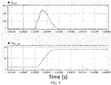
- the current in-rush (i Cout ) is observed on the DC bus capacitor 125 of the secondary converter 120.
- This current in-rush (i Cout ) is illustrated in Fig. 5 along with DC bus voltage (V DC_sec ) across the secondary converter 120 in the DAB3 100.
- Fig. 5 depicts the waveforms of secondary converter 120 in DAB3 100 upon startup of PWM signals for the primary converter 110, where the primary converter 110 is switching at a 50% duty cycle.
- the current in-rush (i Cout ) is sufficiently large that the VDC_sec gets to a nominal value within one PWM switching cycle of DAB3 devices 201, 202, 203, 204, 205, and 206.
- Fig. 5 shows the DC bus capacitor current (i Cout ) and voltage (V DC_sec ) in the phase-shift control mode when the primary converter 110 in the DAB3 converter 100 is modulated with a 50% duty-cycle and the secondary converter 120 is yet to be enabled with no load on the secondary converter 120.
- the scenario depicted in Fig. 5 can be encountered during the startup of a DAB based converter 100.
- Fig. 6 illustrates waveform of the secondary converter 120.
- the DAB3 100 operates in a phase-shift control mode, with both the primary converter 110 and the secondary converter 120 simultaneously PWM enabled with a 50% fixed duty cycle.
- the primary converter devices 201, 202, 203, 204, 205, and 206
- the secondary converter devices 207, 208, 209, 210, 211, and 2112.
- the larger change in currents handled by secondary converter switches can trigger gate drive de-sat faults in the secondary converter 120 of the DAB3 100, resulting in nuisance and unwanted faults at start-up.
- the unwanted faults at startup could lead to customer dissatisfaction.
- the current magnitude handled by power devices is far higher than their rated ampacity, resulting in instant thermal destruction of these power devices (207, 208, 209, 210, 211, and 212). This damage can occur despite the short duration of the large current flow through the devices (207, 208, 209, 210, 211, and 212) in the secondary converter 120.
- the PWM duty cycles can be set to a smaller value.
- the PWM duty cycles cannot be adjusted directly in the application software.
- the PWM duty is set in the control system 140 with a fixed 50% duty in the phase-shift operational control mode and cannot be adjusted directly in the application software.
- the PWM duty cycles can be adjusted by controlling the dead time, or the time between signals. Increasing the dead time can lead to a reduction in the DC bus capacitor current during startup.
- a pre-charge control scheme is applied in order to reduce the capacitor current when PWM signaling is enabled for both the primary converter 110 and the secondary converter 120.
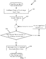
- Fig. 7 depicts a pre-charge control scheme 300.
- the dead time is set to a pre-charge specific dead time.
- the primary drive is enabled.
- the time-based period of the PWM is 20 ⁇ s.
- the time period of the switching ON for a 50% PWM duty is 10 ⁇ s.
- the dead time can be set to 6 ⁇ s.
- Fig. 8 illustrates the DC bus capacitor current (icout) and voltage (v DC_sec ) when the dead time is set to 6 ⁇ s and the PWM frequency is set to 50 kHz in the DAB control system 140.
- the waveforms of the secondary converter 120 in DAB3 100 upon start-up of PWM signals for the primary converter 110 are shown for switching at 20% duty cycle.
- the in-rush current through output capacitor 125 is a magnitude order smaller compared to a 50% duty cycle (see Fig. 5 ). While a 20% duty cycle is used in this example embodiment, the startup mode duty cycle can vary and is set to a value less than the operational mode duty cycle, which can also vary. In one alternative embodiment, the duty cycle can be set between about 15% to 60%.
- Fig. 9 illustrates the results when the secondary converter 120 DC bus is under the pre-charge control scheme 300 with a PWM dead time of 6 ⁇ s followed by normal dead time of 200 ns post pre-charge of the DC bus of the secondary converter 120.
- 'PhA_High_Side_Gate_pri' and 'PhA_Low_Side_Gate_pri' are the primary converter 110 phase A high-side and low-side gate drive commands, e.g. PWM signal.
- the quantity 'i A ' is the phase A current out from the primary converter 110.
- Fig. 9 shows PWM signals for phase A of the primary converter 110 and phase A output current of the primary converter 110.
- Both the primary converter 110 and the secondary converter 120 are operated in phase-shifted mode with 6 ⁇ s dead-time during pre-charge of the DC bus of the secondary converter 120 followed by 200 ns dead time post pre-charge of the DC bus of the secondary converter 120.
- Figs. 10A-10B show the high-side (201) and low-side (202) PWM signals for phase-A of primary converter 110 and primary and secondary currents of the DAB3 100.
- Fig. 10A depicts the waveforms during pre-charge of the DC bus of the secondary converter 120
- Fig. 10B depicts the waveforms during a default 50% duty cycle of the DAB3 100 in phase shift mode. In both examples, the converter 100 is switching but in phase shift mode. More specifically, Figs. 10A-10B illustrate the results when (i) the dead time is set to 6 ⁇ s, resulting in a 20% PWM duty cycle ( Fig.
- Channel 1 (Ch1) is the gate command for switch 201
- Channel 2 (Ch2) is the gate command for switch 202
- Channel 3 (Ch3) is the phase A current (iA) output from the primary converter 110
- Channel 4 (Ch4) is the phase A current (ia) input to the secondary converter 120.
- the startup process for a DAB1 or DAB3 converter 100 can lead to excessive phase-shift.
- the voltage control bandwidth for a closed-loop DC voltage control is typically set to a relatively high value in order to achieve fast dynamics. Due to the high voltage control bandwidth, the phase-shift angle will have a large change during startup. The large phase-shift will require rapid flow of power from the primary converter 110 to the secondary converter 120, which could result in current in-rush (i Cout ) experienced by output capacitor 125 (C out ). A current in-rush (i Cout ) leads to an excessively high peak value of current (i a in Fig. 6 ) flowing at the input of the secondary converter 120.
- the current in-rush (signal i a in Fig. 1 and results shown in Fig. 6 ) will trigger the gate drive de-sat faults in the secondary converter 120 and often this current in-rush will instantly damage some of the power devices (such as 207, 208, 209, 210, 211, and 212) in the secondary converter 120.
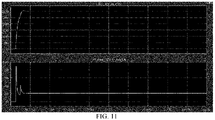
- Fig. 11 illustrates the result for a single-phase DAB converter 100.
- the phase-shift angle changes from 0 degree to the maximum angle (90 degrees) during startup.
- the top waveform is the voltage across the DC bus of the secondary converter 120 and the bottom signal indicates the phase-shift between PWM signals for devices in the primary converter 110 and the secondary converter 120.
- the commanded output voltage for the DAB1 converter 100 is 300 V.
- Fig. 12 illustrates the result for a three-phase DAB converter 100.
- the phase-shift angle changes from 0 degree to the maximum angle (90 degrees) during startup. As shown in Fig.
- the top waveform is the voltage across the DC bus of the secondary converter 120 and the bottom signal indicates the phase-shift between PWM signals for devices in the primary converter 110 and the secondary converter 120.
- the commanded output voltage for the DAB3 converter 100 is 56 V. This abrupt change in phase-shift angle stresses the controller bandwidth in addition to causing an excessive current in-rush (icout) and a large overshoot in the DC voltage output (VDc_sec) of the secondary converter 120.
- the startup control process 400 can be used to prevent excessive phase-shift during startup of a DAB1 converter 100 and a DAB3 converter 100.
- Fig. 13 is a flowchart of the startup process 400, according to one example embodiment. As shown in Fig. 13 , at step 401, the startup process is enabled. The process can be enabled if certain operational parameters are met, such as the measured voltage on the DC bus and the PI gain factor. If the startup control scheme 400 is enabled, at step 402, the normal proportional gain is adjusted. If the startup scheme 400 is not enabled, at step 403, the unadjusted normal proportional gain is used.
- the process 400 limits the bandwidth of the proportional and integral (PI) controller for the DC bus voltage control of the secondary converter 120 in the DAB3 converter 100. Bandwidth is limited by slewing the gains of the PI controller during the startup, preventing large changes in phase-shift angle during startup.
- PI proportional and integral
- the DC bus voltage across the secondary converter 120 is measured. Based on value of V DC_sec , the startup feature is enabled or disabled. To determine whether the startup process should be enabled, the measured DC bus voltage (V DC_sec ) is compared with a voltage threshold and the PI gain factor is compared with a threshold of the PI gain slew limit. When the measured voltage is equal to or less than the voltage threshold and the PI gain factor is equal to or less than the threshold of the PI gain slew limit, the startup feature is enabled; otherwise the startup feature is disabled.
- the Incremental Slew Limiter 150 is used to calculate the PI gain factor.
- the inputs to this Incremental Slew Limiter 150 are the PI gain factor command, PI gain factor slew limit, and PI gain factor initial value.
- the initial value of the PI gain factor is used to set the initial value of the PI gain factor during the startup and the value can be set between 0 and 1;
- the PI gain factor command is set to determine the final value of the PI gain factor and the maximum value is limited to 1;
- the PI gain factor slew limit is set to determine the slew rate of PI gain factor from the initial value to the final value.
- the value of the PI gain factor command can be set between 0 and 1. For example, when the PI gain factor command is set 0.5, the PI gain factor will be slewing from the PI gain factor initial value to 0.5 and limited to 0.5 during the startup. In this example embodiment, the PI gains are limited to 50% of the preset values during the startup. After the measured voltage is greater than the voltage threshold, for example, 90% voltage command, and the PI gain factor is greater than the threshold of the PI gain slew limit, for example, 0.45, the startup control is disabled.
- the PI gains of the DC voltage control are determined by a PI gain factor and the preset PI gains, which means the proportional gain K p equals to PI gain factor times the preset proportional gain K p_Normal , the integral gain K i equals to the PI gain factor times the preset integral gain K i_Normal and the active state feedback gain G v equals to the PI gain factor times the preset gain G v_Nomal .
- K p PI Gain Factor ⁇ K p_Normal
- K i PI Gain Factor ⁇ K i_Normal
- G v PI Gain Factor ⁇ G v_Normal
- the PI gains are the preset PI gains.
- K p K p_Normal
- K i K i _Normal
- G v G v _Normal
- Fig. 14 The result with startup control for a single-phase DAB 100 is shown in Fig. 14 .
- the slew limit of PI gains was set to 2000% per second (or 100% per 50ms)
- the V dc voltage threshold for DAB startup was set to 90% of the V dc command
- G v was set to 50% of K p .
- the slew rate-based control of the phase shift angle between PWM signals for the primary converter 110 and the secondary converter 100 in the DAB1 converter 100 results in a reduced risk of damage to the converter 100 upon startup as compared to a typical startup procedure.
- the results with startup control for a DAB3 converter 100 are shown in Fig. 15 .
- the slew limit of PI gains was set to 200% per second (or 100% per 5 ms)
- the V dc voltage threshold for DAB startup was set to 90% of the V dc command
- G v was set to 50% of K p .
- the DAB converter 100 startup routine includes both processes: pre-charge control 300 and startup control 400.
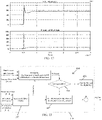
- a flowchart of the DAB startup routine is shown in Fig. 16 .
- the startup routine 500 begins at step 501 by enabling the primary drive 110 and running the converter pre-charge control scheme 300. If the pre-charge completes successfully, the secondary drive is enabled at step 502. Next, the startup control 400 is enabled at step 503. After startup control is completed, the startup routine 500 is ended.
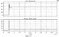
- Fig. 17 shows the results of a DAB3 converter 100 startup with the startup routine 400 disabled.
- Fig. 17 shows the result of a DAD3 converter 100 at start-up without any slew rate control in the PI controller parameters.
- the top waveform is the voltage across the DC bus secondary converter 120 and the bottom signal indicates phase-shift between PWM signals for devices in the primary converter 110 and the secondary converter 120.
- the commanded output voltage for DAB3 converter 100 is 56 V.
- the phase-shift angle increases smoothly, resulting in a reduction in peak current through the DC bus capacitor 125 of the secondary converter 120.
- the pre-charge control is enabled at 5 ms and the PWM duty cycle is set to 20%. At 2 ms, the PWM duty cycle is set to 50%. At 2.5 ms, the phase shifted PWM switching of the secondary converter 120 is enabled and the voltage PI controller is controlling the output voltage to the commanded value.
- the dead-time between the high-side and low-side PWM signals for the primary converter 110 is 6 ⁇ s.
- the duty cycle for PWM signals for the primary converter 110 is tied to 20%.
- PWM signals for the secondary converter 120 are phase-shifted with respect to PWM signals for the primary converter 110, but controlled by slew rate.
- the dead time between the high-side and low-side PWM signals for the primary converter 110 is scaled back to 200 ns, which ensures ⁇ 50% duty cycle for PWM signals for the primary converter 110.
- PWM signals for the secondary converter 120 are phase-shifted with respect to PWM signals and remain within a narrow bound around 10 degrees at a given power. If power on the secondary converter 120 increases, then phase-shift between PWM signals for the primary converter 110 and the secondary converter 120 increases (by a smooth slew rate), resulting stable operation without any risk of current in-rush, excessive DC component in output currents of the primary converter 110, and any over-voltage at output of the secondary converter 120.
- the startup routine 400 for DAB1 and DAB3 converters 100, instant failure in the power devices of the secondary converter 120 can be prevented; a current in-rush through the capacitor 125 in the secondary converter 120 is eliminated; stress on the controller bandwidth of the DAB3 converter 100 is reduced, resulting in an improved design of a closed loop control system for DAB1 and DAB3 converters 100.
- the startup routine 400 provides a trade-off between dynamic and steady state operation of DAB1 and DAB3 converters 100.
- the slew rate in the PI controller parameter ensures that during an abrupt change in the output load, the primary converter does not pass on excessive DC current in the magnetic circuit of the DAB1 and DAB3 converters 100, resulting in magnetic saturation. Otherwise, the converter 100 could experience current in-rush resulting from magnetic saturation, which could lead to thermal failures.
- the routine 400 is simple to implement and can effectively nuisance faults in DAB1 and DAB3 converters 100.
- the invention may also broadly consist in the parts, elements, steps, examples and/or features referred to or indicated in the specification individually or collectively in any and all combinations of two or more said parts, elements, steps, examples and/or features.
- one or more features in any of the embodiments described herein may be combined with one or more features from any other embodiment(s) described herein.
Landscapes
- Engineering & Computer Science (AREA)
- Power Engineering (AREA)
- Dc-Dc Converters (AREA)
Applications Claiming Priority (1)
| Application Number | Priority Date | Filing Date | Title |
|---|---|---|---|
| US202063118629P | 2020-11-25 | 2020-11-25 |
Publications (2)
| Publication Number | Publication Date |
|---|---|
| EP4007148A1 true EP4007148A1 (fr) | 2022-06-01 |
| EP4007148B1 EP4007148B1 (fr) | 2026-04-01 |
Family
ID=77998735
Family Applications (1)
| Application Number | Title | Priority Date | Filing Date |
|---|---|---|---|
| EP21199151.8A Active EP4007148B1 (fr) | 2020-11-25 | 2021-09-27 | Procédé de démarrage d'un convertisseur à double pont actif pour empêcher les défaillances dues à la surtension et l'emballement thermique |
Country Status (2)
| Country | Link |
|---|---|
| US (1) | US11637502B2 (fr) |
| EP (1) | EP4007148B1 (fr) |
Cited By (2)
| Publication number | Priority date | Publication date | Assignee | Title |
|---|---|---|---|---|
| EP4369581A1 (fr) * | 2022-11-08 | 2024-05-15 | Deere & Company | Procédés de commande de perte d'énergie réduite pour convertisseurs cc-cc |
| US20250330097A1 (en) * | 2024-04-18 | 2025-10-23 | King Fahd University Of Petroleum And Minerals | Fault current control of three-phase dual active bridge dc-dc converter employing a novel modified asymmetrical duty cycle control modulation |
Families Citing this family (1)
| Publication number | Priority date | Publication date | Assignee | Title |
|---|---|---|---|---|
| US12431815B2 (en) | 2023-09-06 | 2025-09-30 | Caterpillar Inc. | Start-up control for multilevel dual active bridge converter |
Family Cites Families (4)
| Publication number | Priority date | Publication date | Assignee | Title |
|---|---|---|---|---|
| US10110138B1 (en) * | 2017-05-26 | 2018-10-23 | Cummins Power Generation Ip, Inc. | Soft-starting control method for electrical converter |
| WO2020031807A1 (fr) * | 2018-08-06 | 2020-02-13 | 三菱電機株式会社 | Dispositif de conversion de puissance |
| US11070138B2 (en) | 2019-10-31 | 2021-07-20 | Deere & Company | System for controlling a direct-current-to-direct-current converter to provide electrical energy to a vehicle implement |
| KR102177142B1 (ko) * | 2020-01-09 | 2020-11-10 | 주식회사 효성 | 절연형 양방향 dc-dc 컨버터에서 센서리스 과전류 예측방법 |
-
2021
- 2021-09-24 US US17/484,823 patent/US11637502B2/en active Active
- 2021-09-27 EP EP21199151.8A patent/EP4007148B1/fr active Active
Non-Patent Citations (5)
| Title |
|---|
| ANURAG ANUP ET AL: "Startup Scheme for the Active Front End Converter in a Medium Voltage Mobile Utility Support Equipment based Solid State Transformer (MUSE-SST)", IECON 2020 THE 46TH ANNUAL CONFERENCE OF THE IEEE INDUSTRIAL ELECTRONICS SOCIETY, IEEE, 18 October 2020 (2020-10-18), pages 1487 - 1492, XP033859909, DOI: 10.1109/IECON43393.2020.9254331 * |
| ASKARIAN IMAN ET AL: "Phase-shift frequency-variant control for single stage dual active bridge DC/DC converter over a wide input voltage range", 2015 IEEE INTERNATIONAL TELECOMMUNICATIONS ENERGY CONFERENCE (INTELEC), IEEE, 18 October 2015 (2015-10-18), pages 1 - 5, XP032968738, DOI: 10.1109/INTLEC.2015.7572462 * |
| KWAK BONGWOO ET AL: "Inrush current reduction technology of DAB converter for low-voltage battery systems and DC bus connections in DC microgrids", IET POWER ELECTRONICS, IET, UK, vol. 13, no. 8, 17 June 2020 (2020-06-17), pages 1528 - 1536, XP006090608, ISSN: 1755-4535, DOI: 10.1049/IET-PEL.2019.0506 * |
| SAEED MARIAM ET AL: "Energization and Start-up of Modular Three-stage Solid State Transformers", 2018 IEEE 19TH WORKSHOP ON CONTROL AND MODELING FOR POWER ELECTRONICS (COMPEL), IEEE, 25 June 2018 (2018-06-25), pages 1 - 8, XP033402446, DOI: 10.1109/COMPEL.2018.8460167 * |
| ZHANG XUEYIN ET AL: "A Microprocessor Resource-Saving Dual Active Bridge Control for Startup and Restart of Three-Stage Modular Solid-State Transformer", IEEE TRANSACTIONS ON POWER DELIVERY, IEEE SERVICE CENTER, NEW YORK, NY, US, vol. 35, no. 3, 9 October 2019 (2019-10-09), pages 1443 - 1454, XP011789880, ISSN: 0885-8977, [retrieved on 20200522], DOI: 10.1109/TPWRD.2019.2946463 * |
Cited By (2)
| Publication number | Priority date | Publication date | Assignee | Title |
|---|---|---|---|---|
| EP4369581A1 (fr) * | 2022-11-08 | 2024-05-15 | Deere & Company | Procédés de commande de perte d'énergie réduite pour convertisseurs cc-cc |
| US20250330097A1 (en) * | 2024-04-18 | 2025-10-23 | King Fahd University Of Petroleum And Minerals | Fault current control of three-phase dual active bridge dc-dc converter employing a novel modified asymmetrical duty cycle control modulation |
Also Published As
| Publication number | Publication date |
|---|---|
| US11637502B2 (en) | 2023-04-25 |
| EP4007148B1 (fr) | 2026-04-01 |
| US20220263405A1 (en) | 2022-08-18 |
Similar Documents
| Publication | Publication Date | Title |
|---|---|---|
| US11637502B2 (en) | Startup process for a dual active bridge converter to prevent over-voltage failure and thermal run-away | |
| EP3631959B1 (fr) | Procédé de commande de redémarrage à chaud pour convertisseur électrique | |
| US10525841B2 (en) | Gate driver with short circuit protection | |
| JP5928913B2 (ja) | 共振形dc−dcコンバータの制御装置 | |
| CN104220950B (zh) | 用于恒定电流恒定功率控制的电源控制方法 | |
| US9553540B2 (en) | Power converter with pre-compensation for dead-time insertion | |
| US8525502B2 (en) | Digital pulse-frequency modulation controller for switch-mode power supplies with frequency targeting and ultrasonic modes | |
| US8576581B2 (en) | Circuit for controlling the current in an electrical control member or the voltage across the terminals of said electrical control member | |
| EP2481144B1 (fr) | Démarrage d'un convertisseur cc/cc comprenant un transformateur haute fréquence | |
| US8644035B2 (en) | Load adaptive variable frequency phase-shift full-bridge DC/DC converter | |
| US20190319542A1 (en) | Dc-dc converter and method for operating same | |
| TWI542131B (zh) | 具零電壓切換能力且以穩定切換頻率運作之可切換降壓轉換器 | |
| EP2978120B1 (fr) | Dispositif d'alimentation électrique | |
| US12034365B2 (en) | Soft-start for resonant converters | |
| CN102142777B (zh) | 用于启动直流-直流转换器的方法 | |
| US9917435B1 (en) | Piecewise temperature compensation for power switching devices | |
| US20160036317A1 (en) | Power conversion device | |
| US20240154534A1 (en) | Modulation to extend zero-voltage switching margin for dual-active bridge converter | |
| EP3576281A1 (fr) | Procédé de commande d'onduleur pendant le démarrage et dispositif de commande | |
| EP1503489B1 (fr) | Dispositif et procédé de limitation du rapport cyclique maximal | |
| US10003264B2 (en) | DC/DC converter | |
| US11316423B2 (en) | Half-bridge having power semiconductors | |
| CN104682679B (zh) | 电源转换器及其斜率侦测控制器与方法 | |
| US20050276085A1 (en) | Current control for inductive weld loads | |
| US6535403B1 (en) | Systems and methods for inverter waveform smoothing |
Legal Events
| Date | Code | Title | Description |
|---|---|---|---|
| PUAI | Public reference made under article 153(3) epc to a published international application that has entered the european phase |
Free format text: ORIGINAL CODE: 0009012 |
|
| STAA | Information on the status of an ep patent application or granted ep patent |
Free format text: STATUS: THE APPLICATION HAS BEEN PUBLISHED |
|
| AK | Designated contracting states |
Kind code of ref document: A1 Designated state(s): AL AT BE BG CH CY CZ DE DK EE ES FI FR GB GR HR HU IE IS IT LI LT LU LV MC MK MT NL NO PL PT RO RS SE SI SK SM TR |
|
| STAA | Information on the status of an ep patent application or granted ep patent |
Free format text: STATUS: REQUEST FOR EXAMINATION WAS MADE |
|
| 17P | Request for examination filed |
Effective date: 20221130 |
|
| RBV | Designated contracting states (corrected) |
Designated state(s): AL AT BE BG CH CY CZ DE DK EE ES FI FR GB GR HR HU IE IS IT LI LT LU LV MC MK MT NL NO PL PT RO RS SE SI SK SM TR |
|
| STAA | Information on the status of an ep patent application or granted ep patent |
Free format text: STATUS: EXAMINATION IS IN PROGRESS |
|
| 17Q | First examination report despatched |
Effective date: 20230418 |
|
| GRAP | Despatch of communication of intention to grant a patent |
Free format text: ORIGINAL CODE: EPIDOSNIGR1 |
|
| STAA | Information on the status of an ep patent application or granted ep patent |
Free format text: STATUS: GRANT OF PATENT IS INTENDED |
|
| INTG | Intention to grant announced |
Effective date: 20251030 |
|
| GRAS | Grant fee paid |
Free format text: ORIGINAL CODE: EPIDOSNIGR3 |
|
| GRAA | (expected) grant |
Free format text: ORIGINAL CODE: 0009210 |
|
| STAA | Information on the status of an ep patent application or granted ep patent |
Free format text: STATUS: THE PATENT HAS BEEN GRANTED |
|
| AK | Designated contracting states |
Kind code of ref document: B1 Designated state(s): AL AT BE BG CH CY CZ DE DK EE ES FI FR GB GR HR HU IE IS IT LI LT LU LV MC MK MT NL NO PL PT RO RS SE SI SK SM TR |
|
| REG | Reference to a national code |
Ref country code: CH Ref legal event code: F10 Free format text: ST27 STATUS EVENT CODE: U-0-0-F10-F00 (AS PROVIDED BY THE NATIONAL OFFICE) Effective date: 20260401 Ref country code: GB Ref legal event code: FG4D |
|
| REG | Reference to a national code |
Ref country code: IE Ref legal event code: FG4D |
|
| REG | Reference to a national code |
Ref country code: DE Ref legal event code: R096 Ref document number: 602021051018 Country of ref document: DE |