EP4007162B1 - Audioprozessorschaltung und audioverarbeitungsverfahren - Google Patents
Audioprozessorschaltung und audioverarbeitungsverfahren Download PDFInfo
- Publication number
- EP4007162B1 EP4007162B1 EP21183360.3A EP21183360A EP4007162B1 EP 4007162 B1 EP4007162 B1 EP 4007162B1 EP 21183360 A EP21183360 A EP 21183360A EP 4007162 B1 EP4007162 B1 EP 4007162B1
- Authority
- EP
- European Patent Office
- Prior art keywords
- circuit
- audio
- storage circuit
- digital
- audio data
- Prior art date
- Legal status (The legal status is an assumption and is not a legal conclusion. Google has not performed a legal analysis and makes no representation as to the accuracy of the status listed.)
- Active
Links
Images


Classifications
-
- H—ELECTRICITY
- H04—ELECTRIC COMMUNICATION TECHNIQUE
- H04S—STEREOPHONIC SYSTEMS
- H04S1/00—Two-channel systems
- H04S1/007—Two-channel systems in which the audio signals are in digital form
-
- H—ELECTRICITY
- H03—ELECTRONIC CIRCUITRY
- H03F—AMPLIFIERS
- H03F1/00—Details of amplifiers with only discharge tubes, only semiconductor devices or only unspecified devices as amplifying elements
- H03F1/26—Modifications of amplifiers to reduce influence of noise generated by amplifying elements
-
- G—PHYSICS
- G10—MUSICAL INSTRUMENTS; ACOUSTICS
- G10L—SPEECH ANALYSIS TECHNIQUES OR SPEECH SYNTHESIS; SPEECH RECOGNITION; SPEECH OR VOICE PROCESSING TECHNIQUES; SPEECH OR AUDIO CODING OR DECODING
- G10L19/00—Speech or audio signals analysis-synthesis techniques for redundancy reduction, e.g. in vocoders; Coding or decoding of speech or audio signals, using source filter models or psychoacoustic analysis
- G10L19/012—Comfort noise or silence coding
-
- H—ELECTRICITY
- H03—ELECTRONIC CIRCUITRY
- H03F—AMPLIFIERS
- H03F3/00—Amplifiers with only discharge tubes or only semiconductor devices as amplifying elements
- H03F3/181—Low-frequency amplifiers, e.g. audio preamplifiers
- H03F3/183—Low-frequency amplifiers, e.g. audio preamplifiers with semiconductor devices only
-
- H—ELECTRICITY
- H03—ELECTRONIC CIRCUITRY
- H03M—CODING; DECODING; CODE CONVERSION IN GENERAL
- H03M1/00—Analogue/digital conversion; Digital/analogue conversion
- H03M1/66—Digital/analogue converters
-
- H—ELECTRICITY
- H03—ELECTRONIC CIRCUITRY
- H03F—AMPLIFIERS
- H03F2200/00—Indexing scheme relating to amplifiers
- H03F2200/372—Noise reduction and elimination in amplifier
-
- H—ELECTRICITY
- H04—ELECTRIC COMMUNICATION TECHNIQUE
- H04N—PICTORIAL COMMUNICATION, e.g. TELEVISION
- H04N21/00—Selective content distribution, e.g. interactive television or video on demand [VOD]
- H04N21/40—Client devices specifically adapted for the reception of or interaction with content, e.g. set-top-box [STB]; Operations thereof
- H04N21/43—Processing of content or additional data, e.g. demultiplexing additional data from a digital video stream; Elementary client operations, e.g. monitoring of home network or synchronising decoder's clock; Client middleware
- H04N21/439—Processing of audio elementary streams
- H04N21/4392—Processing of audio elementary streams involving audio buffer management
-
- H—ELECTRICITY
- H04—ELECTRIC COMMUNICATION TECHNIQUE
- H04S—STEREOPHONIC SYSTEMS
- H04S2400/00—Details of stereophonic systems covered by H04S but not provided for in its groups
- H04S2400/13—Aspects of volume control, not necessarily automatic, in stereophonic sound systems
Definitions
- the present disclosure relates to audio technology. More particularly, the present disclosure relates to an audio processor circuit and an audio processing method for reducing noise.
- audio data may be lost or overflowed, and thus noise is generated e.g., during decoding, and affects user's hearing experience.
- Document JP H01213036 describes a voice decoder.
- Document JP 6387060 describes a game machine.
- Some aspects of the present disclosure are to provide an audio processor circuit according to claim 1 and an audio processing method according the independent method claim 7. Further embodiments are set in the dependent claims 2-6 and 8-13.
- the audio processor circuit and the audio processing method of the present disclosure can prevent the user from hearing noise so as to improve the user's hearing experience.
- connection may refer to “electrically connected” or “electrically coupled.”
- Connected may also refer to operations or actions between two or more elements.
- FIG. 1 is a schematic diagram illustrating an audio playing system 100 according to some embodiments of the present disclosure.
- the audio playing system 100 includes an electrical device D1, an audio adapter device D2, and an audio playing device D3.
- the audio adapter device D2 can be coupled between the electrical device D1 and the audio playing device D3.
- the electrical device D1 may be a cell phone, a laptop, a tablet, or other electrical apparatuses which can provide audio data.
- the audio adapter device D2 may be an audio dongle.
- the audio playing device D3 may be headphones/earphones, a speaker, or other playing apparatuses with audio playing functions.
- the audio adapter device D2 can be coupled between the electrical device D1 and the audio playing device D3.
- the electrical device D1 includes a connection portion P1
- the audio adapter device D2 includes a connection portion T1 and a connection portion P2
- the audio playing device D3 includes a connection portion T2.
- a type of the connection portion T1 corresponds to that of the connection portion P1
- a type of the connection portion T2 corresponds to that of the connection portion P2.
- the connection portion P1 is a female connector with Type-C standard
- the connection portion T1 is a male connector with Type-C standard
- the connection portion T1 can be inserted into the connection portion P1.
- the connection portion P2 is a headphones/earphones jack
- the connection portion T2 is a headphones/earphones plug
- the connection portion T2 can be inserted into the connection portion P2.
- the electrical device D1 can be connected to an audio platform to receive audio data from the audio platform. Then, the electrical device D1 can output digital audio data DS to the audio adapter device D2 according to the audio data from the audio platform. In some other embodiments, the digital audio data DS is stored in the electrical device D1.
- the audio adapter device D2 includes an audio processor circuit 200.
- the audio processor circuit 200 can generate an output audio signal OUT according to the digital audio data DS, and provide the output audio signal OUT to an audio playing circuit 300 in the audio playing device D3. Then, the audio playing circuit 300 can play corresponding audio according to the output audio signal OUT.
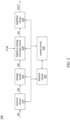
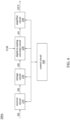
- FIG. 2 is a functional block diagram illustrating the audio processor circuit 200 according to some embodiments of the present disclosure.
- the audio processor circuit 200 includes a receiver circuit 210, a storage circuit 220, a digital-to-analog converter circuit 230, an amplifier circuit 240, a detector circuit 250, and a control circuit 260.
- the storage circuit 220 is coupled to the receiver circuit 210.
- the digital-to-analog converter circuit 230 is coupled to the storage circuit 220.
- the amplifier circuit 240 is coupled to the digital-to-analog converter circuit 230.
- the detector circuit 250 and the control circuit 260 are coupled to the receiver circuit 210, the storage circuit 220, the digital-to-analog converter circuit 230, and the amplifier circuit 240.
- the receiver circuit 210 may be a PHY circuit.
- the storage circuit 220 may be a register that can perform a first-in-first-out (FIFO) process.
- the amplifier circuit 240 may be an audio amplifier.
- the control circuit 260 may be a micro controller unit (MCU).
- the aforementioned implementations of the receiver circuit 210, the storage circuit 220, the amplifier circuit 240, and the control circuit 260 are merely for illustration, and various implementations of the storage circuit 220, the amplifier circuit 240, and the control circuit 260 are within the contemplated scopes of the present disclosure.
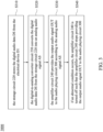
- FIG. 3 is a flow diagram illustrating an audio processing method 3000 according to some embodiments of the present disclosure.
- the audio processing method 3000 includes operations S310, S320, S330, and S340.
- the storage circuit 220 stores the digital audio data DS from the electrical device D1.
- the receiver circuit 210 receives the digital audio data DS from the electrical device D1 first, and then the receiver circuit 210 transmits the digital audio data DS to the storage circuit 220 in order to store the digital audio data DS in the storage circuit 220.
- the digital-to-analog converter circuit 230 converts the digital audio data DS from the storage circuit 220 into an analog audio signal AS.
- the digital-to-analog converter circuit 230 receives the digital audio data DS stored in the storage circuit 220 according to a clock signal CLK, and converts the received digital audio data DS into an analog form in order to generate the analog audio signal AS.
- the amplifier circuit 240 provides the output audio signal OUT to the audio playing circuit 300 according to the analog audio signal AS.
- the amplifier circuit 240 receives the analog audio signal AS and provides the output audio signal OUT to the audio playing circuit 300 according to the analog audio signal AS such that the audio playing device D3 can play corresponding audio according to the output audio signal OUT.
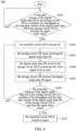
- FIG. 4 is a detailed flow diagram illustrating the operation S340 according to some embodiments of the present disclosure.
- the detector circuit 250 detects whether a total data volume of the digital audio data DS in the storage circuit 220 is a multiple of a throughput or whether the total data volume of the digital audio data DS in the storage circuit 220 is less than an upper limit value.
- the total data volume of the digital audio data DS in the storage circuit 220 will be a multiple of the throughput, in which the throughput may be a product of a channel number and a transmission bit number.
- the throughput may be 48 (the product of 2 and 24) bits.
- the storage circuit 220 receives a multiple of 48 bits per millisecond.
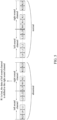
- FIG. 5 is a schematic illustrating a normal data transmission procedure and an abnormal data transmission procedure according to some embodiments of the present disclosure.
- the left sound channel corresponds to 24 bits, e.g., data LO-L23
- the right sound channel corresponds to 24 bits, e.g., data R0-R23.
- the abnormal condition occurs (e.g., one or more bits are lost)
- it will cause sequential errors in the arrangement of the audio data.
- the data R1 of the right sound channel is lost, and this causes the data R0 of the right sound channel to be shifted to fill the vacancy of the data R1 of the right sound channel.
- the data R0 of the right sound channel is shifted to an original position of the data R1 of the right sound channel
- the data L23 of the left sound channel is shifted to the right sound channel.
- the data L22 of the left sound channel is shifted to an original position of the data L23 of the left sound channel, and so on. It causes the arrangement of the data to be wrong and cause the analog audio signal AS passing through the digital-to-analog converter circuit 230 and the amplifier circuit 240 as noise.
- the control circuit 260 turns off the amplifier circuit 240 under a condition that the total data volume of the digital audio data DS in the storage circuit 220 is not a multiple of the throughput (48 bits), such that the amplifier circuit 240 stops providing the output audio signal OUT to the audio playing circuit 300. In some other embodiments, the control circuit 260 turns off the amplifier circuit 240 under a condition that the total data volume of the digital audio data DS in the storage circuit 220 is not a multiple of 48 bits for a time interval.
- the digital-to-analog converter circuit 230 receives the digital audio data DS from the storage circuit 220 according to the clock signal CLK corresponding to a sampling period (e.g., 1 millisecond).
- the aforementioned time interval may be twice (e.g., 2 milliseconds) or more than twice (e.g., more than 2 milliseconds) the sampling period.
- the digital-to-analog converter circuit 230 receives the digital audio data DS from the storage circuit 220 with a sampling period (e.g., 1 millisecond), the total volume per millisecond of the received data received by the storage circuit 220 is equal to a product of one-thousand of the sampling rate, the channel number, and the transmission bit number.
- a sampling period e.g. 1 millisecond
- the storage circuit 220 does not store too much data.
- an abnormal condition e.g., the digital-to-analog converter circuit 230 receives the digital audio data DS from the storage circuit 220 abnormally
- the control circuit 260 turns off the amplifier circuit 240 under a condition that the total data volume of the digital audio data DS in the storage circuit 220 is equal to or greater than the upper limit value such that the amplifier circuit 240 stops providing the output audio signal OUT to the audio playing circuit 300.
- the upper limit value may be 6912 (a product of 3 and 2304) bits or greater than 6912 (a product of 3 and 2304) bits.
- the amplifier circuit 240 is turned off.
- the control circuit 260 turns off the amplifier circuit 240 such that the amplifier circuit 240 stops providing the output audio signal OUT to the audio playing circuit 300. Then, it goes to operation S343.
- the storage circuit 220 stops receiving the digital audio data DS from the electrical device D1.
- the control circuit 260 controls (disables) the receiver circuit 210 to stop transmitting the digital audio data DS to the storage circuit 220. Then, it goes to operation S344.
- the digital audio data DS stored in the storage circuit 220 is erased and the clock signal CLK is reset.
- the control circuit 260 erases the digital audio data DS stored in the storage circuit 220 and resets the clock signal CLK. Then, it goes to operation S345.
- the storage circuit 220 receives the digital audio data DS from the electrical device D1 again.
- the control circuit 260 controls (enables) the receiver circuit 210 to transmit the digital audio data DS to the storage circuit 220 again in the time interval when the electrical device D1 does not transmit any data. Then, it goes to operation S346.
- the detector circuit 250 detects whether the total data volume of the digital audio data DS in the storage circuit 220 is a multiple of the throughput and whether the total data volume of the digital audio data DS in the storage circuit 220 is less than the upper limit value again. If the total data volume of the digital audio data DS in the storage circuit 220 is a multiple of the aforementioned throughput and the total data volume of the digital audio data DS in the storage circuit 220 is less than the aforementioned upper limit value (i.e., the determination result of operation S346 is "YES"), it goes to operations S347. If the determination result of operation S346 is "NO", it returns back to operation S342.
- the amplifier circuit 240 is turned on again.
- the control circuit 260 restarts the amplifier circuit 240 such that the amplifier circuit 240 provides the output audio signal OUT to the audio playing circuit 300 again.
- audio data may be lost or overflowed, and thus noise is generated and affects user's hearing experience.
- it requires user to replay or replug the audio adapter device D2 to reduce the noise.
- the audio processor circuit 200 of the present disclosure can automatically turn off the amplifier circuit 240 under a condition that the total data volume of the digital audio data DS in the storage circuit 220 is not a multiple of the throughput or the total data volume of the digital audio data DS in the storage circuit 220 is equal to or greater than the upper limit value such that the amplifier circuit 240 stops providing the output audio signal OUT to the audio playing circuit 300.
- the amplifier circuit 240 stops providing the output audio signal OUT to the audio playing circuit 300.
- it can prevent the user from hearing noise so as to improve the user's hearing experience.
- FIG. 6 is a functional block diagram illustrating an audio processor circuit 200A according to some embodiments of the present disclosure.
- the aforementioned operations can be executed by firmware.
- a control circuit 560 can cooperate with related code to detect and control the receiver circuit 210, the storage circuit 220, the digital-to-analog converter circuit 230, and the amplifier circuit 240.
- Other operation principles of the audio processor circuit 200A in FIG. 6 are similar to those of the audio processor circuit 200 in FIG. 2 , so they are not described herein again.
- FIG. 7 is a schematic diagram illustrating an audio playing system 700 according to some embodiments of the present disclosure.
- the audio processor circuit 200 (or 200A) and the audio playing circuit 300 are integrated together in an audio playing device D3 in FIG. 7 .
- a connection portion T2 of the audio playing circuit 300 can be inserted into a connection portion P1 of the electrical device D1 in order to directly couple the electrical device D1 without a coupled between an audio adapter device (as the audio adapter device D2 shown in FIG. 1 ) and the electrical device D1.
- a type of the connection portion T2 of the audio playing circuit 300 corresponds to the type of the connection portion P1.
- the operations of the audio processor circuit 200 (or 200A) in FIG. 7 are similar to those of the audio processor circuit 200 (or 200A) in FIG. 2 (or FIG. 6 ), so they are not described herein again.
- the audio processor circuit and the audio processing method of the present disclosure can prevent the user from hearing noise so as to improve the user's hearing experience.
Landscapes
- Engineering & Computer Science (AREA)
- Multimedia (AREA)
- Power Engineering (AREA)
- Physics & Mathematics (AREA)
- Signal Processing (AREA)
- Acoustics & Sound (AREA)
- Health & Medical Sciences (AREA)
- Human Computer Interaction (AREA)
- Audiology, Speech & Language Pathology (AREA)
- Theoretical Computer Science (AREA)
- Computational Linguistics (AREA)
- Circuit For Audible Band Transducer (AREA)
- Reverberation, Karaoke And Other Acoustics (AREA)
- Amplifiers (AREA)
Claims (13)
- Audioprozessorschaltung (200), aufweisendeine Speicherschaltung (220), die konfiguriert ist zum Speichern von digitalen Audiodaten (DS) von einer elektrischen Vorrichtung (D1);eine Digital-Analog-Wandlerschaltung (230), die konfiguriert ist zum Umwandeln der digitalen Audiodaten (DS) von der Speicherschaltung (220) in ein analoges Audiosignal (AS); undeine Verstärkerschaltung (240), die die konfiguriert ist zum Vorsehen eines Audioausgangssignals (OUT) an eine Audiowiedergabeschaltung (300) gemäß dem analogen Audiosignal (AS),eine Detektorschaltung (250), die konfiguriert ist zum Detektieren ob ein Gesamtdatenvolumen der in der Speicherschaltung (220) gespeicherten digitalen Audiodaten (DS) ein Vielfaches eines Durchsatzes ist und ob das Gesamtdatenvolumen der in der Speicherschaltung (220) gespeicherten digitalen Audiodaten (DS) kleiner als ein oberer Grenzwert ist;wobei, wenn detektiert wird, dass das Gesamtdatenvolumen der in der Speicherschaltung (220) gespeicherten digitalen Audiodaten (DS) nicht das Vielfache des Durchsatzes ist oder das Gesamtdatenvolumen der in der Speicherschaltung (220) gespeicherten digitalen Audiodaten (DS) gleich oder größer als der obere Grenzwert ist, die Verstärkerschaltung (240) konfiguriert ist ausgeschaltet zu werden, so dass die Verstärkerschaltung die Bereitstellung des Audioausgangssignals (OUT) an die Audiowiedergabeschaltung (300) einstellt,wobei der Durchsatz ein Produkt aus einer Kanalzahl der Audiowiedergabeschaltung (300) und einer Übertragungsbitzahl jedes Kanals ist, undwobei der obere Grenzwert gleich oder größer als das Dreifache des Durchsatzes ist.
- Audioprozessorschaltung (200) nach Anspruch 1, dadurch gekennzeichnet, dass, wenn das Gesamtdatenvolumen der in der Speicherschaltung (220) gespeicherten digitalen Audiodaten (DS) nicht ein Vielfaches des Durchsatzes für ein Zeitintervall ist, die Verstärkerschaltung (240) ausgeschaltet wird, so dass die Verstärkerschaltung (240) die Bereitstellung des Audioausgangssignals (OUT) einstellt, wobei die Digital-Analog-Wandlerschaltung (230) die digitalen Audiodaten (DS) von der Speicherschaltung (220) mit einer Tastperiode empfängt, wobei das Zeitintervall gleich oder größer als das Doppelte der Tastperiode ist.
- Audioprozessorschaltung (200) nach Anspruch 1 oder 2, dadurch gekennzeichnet, dass sie ferner Folgendes aufweist:
eine Detektorschaltung (250), die konfiguriert ist zum Detektieren, ob das Gesamtdatenvolumen der in der Speicherschaltung (220) gespeicherten digitalen Audiodaten (DS) das Vielfache des Durchsatzes ist oder ob das Gesamtdatenvolumen der in der Speicherschaltung (220) gespeicherten digitalen Audiodaten (DS) kleiner als der obere Grenzwert ist. - Audioprozessorschaltung (200) nach Anspruch 1 oder 2, dadurch gekennzeichnet, dass sie ferner Folgendes aufweist:
eine Steuerschaltung (260), die konfiguriert ist zum Abschalten der Verstärkerschaltung (240), so dass die Verstärkerschaltung (240) die Bereitstellung des Audioausgangssignals (OUT) einstellt, zum Steuern die Speicherschaltung (220) so, dass sie den Empfang der digitalen Audiodaten (DS) einstellt, die in der Speicherschaltung (220) gespeicherten digitalen Audiodaten (DS) löscht, ein Taktsignal (CLK) zurücksetzt und zum Steuern der Speicherschaltung (220) so, dass sie die digitalen Audiodaten (DS) erneut empfängt, wobei die Digital-Analog-Wandlerschaltung (230) so konfiguriert ist, dass sie die in der Speicherschaltung (220) gespeicherten digitalen Audiodaten (DS) gemäß dem Taktsignal (CLK) empfängt. - Audioprozessorschaltung (200) nach Anspruch 4, dadurch gekennzeichnet, dass, nachdem die Steuerschaltung (260) die Speicherschaltung (220) so steuert, dass sie die digitalen Audiodaten (DS) erneut empfängt, die Steuerschaltung (260) die Verstärkerschaltung (240) erneut einschaltet, wenn das Gesamtdatenvolumen der in der Speicherschaltung (220) gespeicherten digitalen Audiodaten (DS) ein Vielfaches des Durchsatzes ist und das Gesamtdatenvolumen der in der Speicherschaltung (220) gespeicherten digitalen Audiodaten (DS) kleiner als der obere Grenzwert ist.
- Audioprozessorschaltung (200) nach Anspruch 1 oder 2, dadurch gekennzeichnet, dass die Audioprozessorschaltung (200) in einer Audioadaptervorrichtung (D2) angeordnet ist, die Audiowiedergabeschaltung (300) in einer Audiowiedergabevorrichtung (D3) angeordnet ist und die Audioadaptervorrichtung (D2) zwischen der elektrischen Vorrichtung (D1) und der Audiowiedergabevorrichtung (D3) gekoppelt ist.
- Audioverarbeitungsverfahren, aufweisendSpeichern von digitalen Audiodaten (DS) von einer elektrischen Vorrichtung (D1) durch eine Speicherschaltung (220);Umwandeln der digitalen Audiodaten (DS) von der Speicherschaltung (220) in ein analoges Audiosignal (AS) durch eine Digital-Analog-Wandlerschaltung (230);Vorsehen eines Audioausgangssignals (OUT) an eine Audiowiedergabeschaltung (300) gemäß dem analogen Audiosignal (AS) durch eine Verstärkerschaltung (240); undKonfigurieren einer Detektorschaltung (250), um zu detektieren, ob ein Gesamtdatenvolumen der Audiodaten (DS), die in der Speicherschaltung (220) gespeichert sind, ein Vielfaches eines Durchsatzes ist und, ob das Gesamtdatenvolumen der digitalen Audiodaten (DS), die in der Speicherschaltung (220) gespeichert sind, kleiner als ein oberer Grenzwert ist;Abschalten der Verstärkerschaltung (240), so dass die Verstärkerschaltung (240) das Vorsehen des Audioausgangssignals (OUT) an die Audiowiedergabeschaltung (300) einstellt, wenn detektiert wird, dass ein Gesamtdatenvolumen der in der Speicherschaltung (220) gespeicherten digitalen Audiodaten (DS) kein Vielfaches des Durchsatzes ist oder das Gesamtdatenvolumen der in der Speicherschaltung (220) gespeicherten digitalen Audiodaten (DS) gleich oder größer als der obere Grenzwert ist,wobei der Durchsatz ein Produkt aus einer Kanalzahl der Audiowiedergabeschaltung (300) und einer Übertragungsbitzahl jedes Kanals ist, undwobei der obere Grenzwert gleich oder größer als das Dreifache des Durchsatzes ist.
- Audioverarbeitungsverfahren nach Anspruch 7, dadurch gekennzeichnet, dass es ferner Folgendes aufweist:Empfangen, durch die Digital-Analog-Wandlerschaltung (230), der digitalen Audiodaten (DS) von der Speicherschaltung (220) mit einer Tastperiode; undAbschalten der Verstärkerschaltung (240), so dass die Verstärkerschaltung (240) das Vorsehen des Ausgangsaudiosignals (OUT) einstellt, wenn das Gesamtdatenvolumen der in der Speicherschaltung (220) gespeicherten digitalen Audiodaten (DS) nicht ein Vielfaches des Durchsatzes für ein Zeitintervall ist, wobei das Zeitintervall gleich oder größer als das Doppelte der Abtastperiode ist, wobei der obere Grenzwert gleich oder größer als das Dreifache eines Durchsatzes der Abtastperiode ist.
- Audioverarbeitungsverfahren nach Anspruch 7 oder 8, dadurch gekennzeichnet, dass es ferner Folgendes aufweist:
Detektieren, durch eine Detektorschaltung (250), ob das Gesamtdatenvolumen der in der Speicherschaltung (220) gespeicherten digitalen Audiodaten (DS) ein Vielfaches des Durchsatzes ist oder ob das Gesamtdatenvolumen der digitalen Audiodaten (DS), die in der Speicherschaltung (220) gespeichert sind, kleiner als der obere Grenzwert ist. - Audioverarbeitungsverfahren nach Anspruch 7 oder 8, dadurch gekennzeichnet, dass es ferner Folgendes aufweist:Abschalten der Verstärkerschaltung (240) durch eine Steuerschaltung (260), so dass die Verstärkerschaltung (240) die Bereitstellung des Audioausgangssignals (OUT) einstellt;Steuern der Speicherschaltung (220) durch die Steuerschaltung (260) so, dass sie den Empfang der digitalen Audiodaten (DS) einsntellt;Löschen der in der Speicherschaltung (220) gespeicherten digitalen Audiodaten (DS) durch die Steuerschaltung (260) und Zurücksetzen eines Taktsignals (CLK) durch die Steuerschaltung (260), wobei die Digital-Analog-Wandlerschaltung (230) so konfiguriert ist, dass sie die in der Speicherschaltung (220) gespeicherten digitalen Audiodaten (DS) gemäß dem Taktsignal (CLK) empfängt; undSteuern der Speicherschaltung (220) durch die Steuerschaltung (260) so, dass sie die digitalen Audiodaten (DS) erneut empfängt.
- Audioverarbeitungsverfahren nach Anspruch 10, dadurch gekennzeichnet, dass es ferner Folgendes aufweist:
nachdem die Steuerschaltung (260) die Speicherschaltung (220) so steuert, dass sie die digitalen Audiodaten (DS) erneut empfängt, erneutes Einschalten der Verstärkerschaltung (240) durch die Steuerschaltung (260), wenn das Gesamtdatenvolumen der in der Speicherschaltung (220) gespeicherten digitalen Audiodaten (DS) ein Vielfaches des Durchsatzes ist, und das Gesamtdatenvolumen der in der Speicherschaltung (220) gespeicherten digitalen Audiodaten (DS) kleiner als der obere Grenzwert ist. - Audioverarbeitungsverfahren nach Anspruch 7 oder 8, dadurch gekennzeichnet, dass die Speicherschaltung (220), die Digital-Analog-Wandlerschaltung (230) und die Verstärkerschaltung (240) in einer Audioadaptervorrichtung (D2) angeordnet sind, die Audiowiedergabeschaltung (300) in einer Audiowiedergabevorrichtung (D3) angeordnet ist und die Audioadaptervorrichtung (D2) zwischen der elektrischen Vorrichtung (D1) und der Audiowiedergabevorrichtung (D3) gekoppelt ist.
- Audioverarbeitungsverfahren nach Anspruch 7 oder 8, dadurch gekennzeichnet, dass die Speicherschaltung (220), die Digital-Analog-Wandlerschaltung (230), die Verstärkerschaltung (240) und die Audiowiedergabeschaltung (300) in einer Audiowiedergabevorrichtung (D3) angeordnet sind.
Applications Claiming Priority (1)
| Application Number | Priority Date | Filing Date | Title |
|---|---|---|---|
| TW109141313A TWI760939B (zh) | 2020-11-25 | 2020-11-25 | 音訊處理電路以及音訊處理方法 |
Publications (2)
| Publication Number | Publication Date |
|---|---|
| EP4007162A1 EP4007162A1 (de) | 2022-06-01 |
| EP4007162B1 true EP4007162B1 (de) | 2025-05-14 |
Family
ID=76764862
Family Applications (1)
| Application Number | Title | Priority Date | Filing Date |
|---|---|---|---|
| EP21183360.3A Active EP4007162B1 (de) | 2020-11-25 | 2021-07-02 | Audioprozessorschaltung und audioverarbeitungsverfahren |
Country Status (5)
| Country | Link |
|---|---|
| US (1) | US11456706B2 (de) |
| EP (1) | EP4007162B1 (de) |
| JP (1) | JP7293278B2 (de) |
| KR (1) | KR102509673B1 (de) |
| TW (1) | TWI760939B (de) |
Families Citing this family (2)
| Publication number | Priority date | Publication date | Assignee | Title |
|---|---|---|---|---|
| TWI857482B (zh) * | 2023-02-07 | 2024-10-01 | 瑞昱半導體股份有限公司 | 播放電路、錄音電路及音訊晶片 |
| CN117316169B (zh) * | 2023-11-28 | 2024-09-06 | 深圳市东明炬创电子股份有限公司 | 音频数据处理方法、装置、设备及计算机可读存储介质 |
Citations (1)
| Publication number | Priority date | Publication date | Assignee | Title |
|---|---|---|---|---|
| WO1993019545A1 (en) * | 1992-03-16 | 1993-09-30 | Scientific-Atlanta, Inc. | Digital audio data muting system and method |
Family Cites Families (14)
| Publication number | Priority date | Publication date | Assignee | Title |
|---|---|---|---|---|
| JPS5753806A (en) * | 1980-09-16 | 1982-03-31 | Toshiba Corp | Processor of digital signal |
| JPH01213036A (ja) | 1988-02-22 | 1989-08-25 | Victor Co Of Japan Ltd | 音声デコーダ |
| JP3381851B2 (ja) * | 1992-07-04 | 2003-03-04 | ソニー株式会社 | 光デイスク装置 |
| JPH06176493A (ja) * | 1992-12-08 | 1994-06-24 | Matsushita Electric Ind Co Ltd | 情報再生装置 |
| JPH1093927A (ja) * | 1996-09-17 | 1998-04-10 | Sony Corp | データ処理監視装置およびデータエラー検出方法 |
| JP2001111499A (ja) | 1999-10-08 | 2001-04-20 | Hitachi Kokusai Electric Inc | 音声復号装置 |
| DK1340320T3 (da) * | 2000-11-30 | 2009-02-23 | Intrasonics Ltd | Apparat og system til anvendelse af datasignaler indlejret i et akustisk signal |
| JP2007194845A (ja) * | 2006-01-18 | 2007-08-02 | Sony Corp | コンテンツ再生システム及びコンテンツ再生方法 |
| JP2008269750A (ja) * | 2007-04-25 | 2008-11-06 | Funai Electric Co Ltd | 光ディスク装置 |
| JP2010118761A (ja) | 2008-11-11 | 2010-05-27 | Sharp Corp | 音声出力装置 |
| US9590648B2 (en) * | 2014-11-07 | 2017-03-07 | John Howard La Grou | Multi-path digital-to-analog converter |
| US9799349B2 (en) * | 2015-04-24 | 2017-10-24 | Cirrus Logic, Inc. | Analog-to-digital converter (ADC) dynamic range enhancement for voice-activated systems |
| JP6387060B2 (ja) * | 2016-09-20 | 2018-09-05 | 株式会社藤商事 | 遊技機 |
| EP3529800B1 (de) * | 2016-10-24 | 2023-04-19 | Avnera Corporation | Erkennung von kopfhörern ausserhalb des ohrs |
-
2020
- 2020-11-25 TW TW109141313A patent/TWI760939B/zh active
-
2021
- 2021-03-29 JP JP2021055252A patent/JP7293278B2/ja active Active
- 2021-05-28 US US17/333,210 patent/US11456706B2/en active Active
- 2021-07-01 KR KR1020210086550A patent/KR102509673B1/ko active Active
- 2021-07-02 EP EP21183360.3A patent/EP4007162B1/de active Active
Patent Citations (1)
| Publication number | Priority date | Publication date | Assignee | Title |
|---|---|---|---|---|
| WO1993019545A1 (en) * | 1992-03-16 | 1993-09-30 | Scientific-Atlanta, Inc. | Digital audio data muting system and method |
Also Published As
| Publication number | Publication date |
|---|---|
| JP2022083957A (ja) | 2022-06-06 |
| KR20220072716A (ko) | 2022-06-02 |
| US20220166387A1 (en) | 2022-05-26 |
| US11456706B2 (en) | 2022-09-27 |
| TW202221699A (zh) | 2022-06-01 |
| JP7293278B2 (ja) | 2023-06-19 |
| KR102509673B1 (ko) | 2023-03-15 |
| TWI760939B (zh) | 2022-04-11 |
| EP4007162A1 (de) | 2022-06-01 |
Similar Documents
| Publication | Publication Date | Title |
|---|---|---|
| US7340272B2 (en) | Mobile communication terminal having a three-dimensional surround sound effect and its control method | |
| EP4007162B1 (de) | Audioprozessorschaltung und audioverarbeitungsverfahren | |
| US7957549B2 (en) | Acoustic apparatus and method of controlling an acoustic apparatus | |
| EP2632177B1 (de) | Elektronische Vorrichtung, Zubehör und Verfahren zum Erkennen des Zubehörs | |
| US10642570B2 (en) | Digital accessory interface calibration | |
| EP2290813A1 (de) | Lautstärkeneinstellungsvorrichtung | |
| US10218535B2 (en) | Low power bidirectional bus | |
| US20180307555A1 (en) | Transfer of data with check bits | |
| US11089429B1 (en) | Indication for correct audio device orientation | |
| US10042796B2 (en) | Digital accessory interface calibration | |
| US6580903B2 (en) | Circuit and method for recording and playing back voice and other sounds in digital mobile radio devices | |
| CN114584899B (zh) | 音频处理电路以及音频处理方法 | |
| US5675641A (en) | Dual-mode speaker telephone | |
| US6711545B1 (en) | Hand-held transmitter having speech storage actuated by transmission failure | |
| JP5914893B2 (ja) | インターホンシステム | |
| US10310577B2 (en) | Power communication apparatus using microphone jack | |
| GB2538245A (en) | Digital accessory interface | |
| KR102464972B1 (ko) | 자동 활성화 마이크의 초기 음성 신호를 인식하기 위한 음성 신호의 제어 및 동기화 방법 및 장치 | |
| KR20010056556A (ko) | 전자교환기의 가상 녹음부를 구비한 안내방송 장치 | |
| JP4489980B2 (ja) | フレーム同期回路 | |
| US11681489B2 (en) | Circuit and method for controlling audio adapter | |
| KR100693589B1 (ko) | 음원 데이터의 동시 재생이 가능한 무선통신 단말기 및 그 방법 | |
| KR100435992B1 (ko) | 다채널 오디오 디텍터의 신호전달 장치 및 방법 | |
| HK40059909B (en) | Audio playing method, earphone box, wireless earphone and earphone suite | |
| JP2001217736A (ja) | ディジタル通信システムにおける切り換え制御方法 |
Legal Events
| Date | Code | Title | Description |
|---|---|---|---|
| PUAI | Public reference made under article 153(3) epc to a published international application that has entered the european phase |
Free format text: ORIGINAL CODE: 0009012 |
|
| STAA | Information on the status of an ep patent application or granted ep patent |
Free format text: STATUS: THE APPLICATION HAS BEEN PUBLISHED |
|
| AK | Designated contracting states |
Kind code of ref document: A1 Designated state(s): AL AT BE BG CH CY CZ DE DK EE ES FI FR GB GR HR HU IE IS IT LI LT LU LV MC MK MT NL NO PL PT RO RS SE SI SK SM TR |
|
| STAA | Information on the status of an ep patent application or granted ep patent |
Free format text: STATUS: REQUEST FOR EXAMINATION WAS MADE |
|
| STAA | Information on the status of an ep patent application or granted ep patent |
Free format text: STATUS: EXAMINATION IS IN PROGRESS |
|
| 17P | Request for examination filed |
Effective date: 20220719 |
|
| RBV | Designated contracting states (corrected) |
Designated state(s): AL AT BE BG CH CY CZ DE DK EE ES FI FR GB GR HR HU IE IS IT LI LT LU LV MC MK MT NL NO PL PT RO RS SE SI SK SM TR |
|
| 17Q | First examination report despatched |
Effective date: 20220803 |
|
| GRAP | Despatch of communication of intention to grant a patent |
Free format text: ORIGINAL CODE: EPIDOSNIGR1 |
|
| STAA | Information on the status of an ep patent application or granted ep patent |
Free format text: STATUS: GRANT OF PATENT IS INTENDED |
|
| INTG | Intention to grant announced |
Effective date: 20250227 |
|
| GRAS | Grant fee paid |
Free format text: ORIGINAL CODE: EPIDOSNIGR3 |
|
| GRAA | (expected) grant |
Free format text: ORIGINAL CODE: 0009210 |
|
| STAA | Information on the status of an ep patent application or granted ep patent |
Free format text: STATUS: THE PATENT HAS BEEN GRANTED |
|
| P01 | Opt-out of the competence of the unified patent court (upc) registered |
Free format text: CASE NUMBER: APP_13894/2025 Effective date: 20250321 |
|
| AK | Designated contracting states |
Kind code of ref document: B1 Designated state(s): AL AT BE BG CH CY CZ DE DK EE ES FI FR GB GR HR HU IE IS IT LI LT LU LV MC MK MT NL NO PL PT RO RS SE SI SK SM TR |
|
| REG | Reference to a national code |
Ref country code: GB Ref legal event code: FG4D |
|
| REG | Reference to a national code |
Ref country code: CH Ref legal event code: EP |
|
| REG | Reference to a national code |
Ref country code: IE Ref legal event code: FG4D |
|
| REG | Reference to a national code |
Ref country code: DE Ref legal event code: R096 Ref document number: 602021030693 Country of ref document: DE |
|
| PGFP | Annual fee paid to national office [announced via postgrant information from national office to epo] |
Ref country code: GB Payment date: 20250626 Year of fee payment: 5 |
|
| PGFP | Annual fee paid to national office [announced via postgrant information from national office to epo] |
Ref country code: FR Payment date: 20250623 Year of fee payment: 5 |
|
| REG | Reference to a national code |
Ref country code: NL Ref legal event code: MP Effective date: 20250514 |
|
| PG25 | Lapsed in a contracting state [announced via postgrant information from national office to epo] |
Ref country code: FI Free format text: LAPSE BECAUSE OF FAILURE TO SUBMIT A TRANSLATION OF THE DESCRIPTION OR TO PAY THE FEE WITHIN THE PRESCRIBED TIME-LIMIT Effective date: 20250514 Ref country code: PT Free format text: LAPSE BECAUSE OF FAILURE TO SUBMIT A TRANSLATION OF THE DESCRIPTION OR TO PAY THE FEE WITHIN THE PRESCRIBED TIME-LIMIT Effective date: 20250915 Ref country code: ES Free format text: LAPSE BECAUSE OF FAILURE TO SUBMIT A TRANSLATION OF THE DESCRIPTION OR TO PAY THE FEE WITHIN THE PRESCRIBED TIME-LIMIT Effective date: 20250514 |
|
| PGFP | Annual fee paid to national office [announced via postgrant information from national office to epo] |
Ref country code: DE Payment date: 20250624 Year of fee payment: 5 |
|
| REG | Reference to a national code |
Ref country code: LT Ref legal event code: MG9D |
|
| PG25 | Lapsed in a contracting state [announced via postgrant information from national office to epo] |
Ref country code: NO Free format text: LAPSE BECAUSE OF FAILURE TO SUBMIT A TRANSLATION OF THE DESCRIPTION OR TO PAY THE FEE WITHIN THE PRESCRIBED TIME-LIMIT Effective date: 20250814 Ref country code: GR Free format text: LAPSE BECAUSE OF FAILURE TO SUBMIT A TRANSLATION OF THE DESCRIPTION OR TO PAY THE FEE WITHIN THE PRESCRIBED TIME-LIMIT Effective date: 20250815 |
|
| PG25 | Lapsed in a contracting state [announced via postgrant information from national office to epo] |
Ref country code: NL Free format text: LAPSE BECAUSE OF FAILURE TO SUBMIT A TRANSLATION OF THE DESCRIPTION OR TO PAY THE FEE WITHIN THE PRESCRIBED TIME-LIMIT Effective date: 20250514 Ref country code: PL Free format text: LAPSE BECAUSE OF FAILURE TO SUBMIT A TRANSLATION OF THE DESCRIPTION OR TO PAY THE FEE WITHIN THE PRESCRIBED TIME-LIMIT Effective date: 20250514 |
|
| REG | Reference to a national code |
Ref country code: AT Ref legal event code: MK05 Ref document number: 1795685 Country of ref document: AT Kind code of ref document: T Effective date: 20250514 |
|
| PG25 | Lapsed in a contracting state [announced via postgrant information from national office to epo] |
Ref country code: BG Free format text: LAPSE BECAUSE OF FAILURE TO SUBMIT A TRANSLATION OF THE DESCRIPTION OR TO PAY THE FEE WITHIN THE PRESCRIBED TIME-LIMIT Effective date: 20250514 |
|
| PG25 | Lapsed in a contracting state [announced via postgrant information from national office to epo] |
Ref country code: HR Free format text: LAPSE BECAUSE OF FAILURE TO SUBMIT A TRANSLATION OF THE DESCRIPTION OR TO PAY THE FEE WITHIN THE PRESCRIBED TIME-LIMIT Effective date: 20250514 |
|
| PG25 | Lapsed in a contracting state [announced via postgrant information from national office to epo] |
Ref country code: AT Free format text: LAPSE BECAUSE OF FAILURE TO SUBMIT A TRANSLATION OF THE DESCRIPTION OR TO PAY THE FEE WITHIN THE PRESCRIBED TIME-LIMIT Effective date: 20250514 |
|
| PG25 | Lapsed in a contracting state [announced via postgrant information from national office to epo] |
Ref country code: RS Free format text: LAPSE BECAUSE OF FAILURE TO SUBMIT A TRANSLATION OF THE DESCRIPTION OR TO PAY THE FEE WITHIN THE PRESCRIBED TIME-LIMIT Effective date: 20250814 |
|
| PG25 | Lapsed in a contracting state [announced via postgrant information from national office to epo] |
Ref country code: IS Free format text: LAPSE BECAUSE OF FAILURE TO SUBMIT A TRANSLATION OF THE DESCRIPTION OR TO PAY THE FEE WITHIN THE PRESCRIBED TIME-LIMIT Effective date: 20250914 |
|
| PG25 | Lapsed in a contracting state [announced via postgrant information from national office to epo] |
Ref country code: LV Free format text: LAPSE BECAUSE OF FAILURE TO SUBMIT A TRANSLATION OF THE DESCRIPTION OR TO PAY THE FEE WITHIN THE PRESCRIBED TIME-LIMIT Effective date: 20250514 |
|
| PG25 | Lapsed in a contracting state [announced via postgrant information from national office to epo] |
Ref country code: DK Free format text: LAPSE BECAUSE OF FAILURE TO SUBMIT A TRANSLATION OF THE DESCRIPTION OR TO PAY THE FEE WITHIN THE PRESCRIBED TIME-LIMIT Effective date: 20250514 Ref country code: SM Free format text: LAPSE BECAUSE OF FAILURE TO SUBMIT A TRANSLATION OF THE DESCRIPTION OR TO PAY THE FEE WITHIN THE PRESCRIBED TIME-LIMIT Effective date: 20250514 |
|
| PG25 | Lapsed in a contracting state [announced via postgrant information from national office to epo] |
Ref country code: CZ Free format text: LAPSE BECAUSE OF FAILURE TO SUBMIT A TRANSLATION OF THE DESCRIPTION OR TO PAY THE FEE WITHIN THE PRESCRIBED TIME-LIMIT Effective date: 20250514 |
|
| PG25 | Lapsed in a contracting state [announced via postgrant information from national office to epo] |
Ref country code: EE Free format text: LAPSE BECAUSE OF FAILURE TO SUBMIT A TRANSLATION OF THE DESCRIPTION OR TO PAY THE FEE WITHIN THE PRESCRIBED TIME-LIMIT Effective date: 20250514 |
|
| PG25 | Lapsed in a contracting state [announced via postgrant information from national office to epo] |
Ref country code: RO Free format text: LAPSE BECAUSE OF FAILURE TO SUBMIT A TRANSLATION OF THE DESCRIPTION OR TO PAY THE FEE WITHIN THE PRESCRIBED TIME-LIMIT Effective date: 20250514 Ref country code: SK Free format text: LAPSE BECAUSE OF FAILURE TO SUBMIT A TRANSLATION OF THE DESCRIPTION OR TO PAY THE FEE WITHIN THE PRESCRIBED TIME-LIMIT Effective date: 20250514 |
|
| PG25 | Lapsed in a contracting state [announced via postgrant information from national office to epo] |
Ref country code: IT Free format text: LAPSE BECAUSE OF FAILURE TO SUBMIT A TRANSLATION OF THE DESCRIPTION OR TO PAY THE FEE WITHIN THE PRESCRIBED TIME-LIMIT Effective date: 20250514 |
|
| REG | Reference to a national code |
Ref country code: DE Ref legal event code: R097 Ref document number: 602021030693 Country of ref document: DE |
|
| REG | Reference to a national code |
Ref country code: CH Ref legal event code: H13 Free format text: ST27 STATUS EVENT CODE: U-0-0-H10-H13 (AS PROVIDED BY THE NATIONAL OFFICE) Effective date: 20260224 |
|
| PG25 | Lapsed in a contracting state [announced via postgrant information from national office to epo] |
Ref country code: LU Free format text: LAPSE BECAUSE OF NON-PAYMENT OF DUE FEES Effective date: 20250702 |
|
| PLBE | No opposition filed within time limit |
Free format text: ORIGINAL CODE: 0009261 |
|
| STAA | Information on the status of an ep patent application or granted ep patent |
Free format text: STATUS: NO OPPOSITION FILED WITHIN TIME LIMIT |
|
| REG | Reference to a national code |
Ref country code: CH Ref legal event code: L10 Free format text: ST27 STATUS EVENT CODE: U-0-0-L10-L00 (AS PROVIDED BY THE NATIONAL OFFICE) Effective date: 20260325 |
|
| REG | Reference to a national code |
Ref country code: BE Ref legal event code: MM Effective date: 20250731 |
|
| PG25 | Lapsed in a contracting state [announced via postgrant information from national office to epo] |
Ref country code: BE Free format text: LAPSE BECAUSE OF NON-PAYMENT OF DUE FEES Effective date: 20250731 |
|
| 26N | No opposition filed |
Effective date: 20260217 |
|
| PG25 | Lapsed in a contracting state [announced via postgrant information from national office to epo] |
Ref country code: CH Free format text: LAPSE BECAUSE OF NON-PAYMENT OF DUE FEES Effective date: 20250731 |