EP4007166B1 - Pwm-ansteuerschaltung und -verfahren - Google Patents
Pwm-ansteuerschaltung und -verfahren Download PDFInfo
- Publication number
- EP4007166B1 EP4007166B1 EP21202997.9A EP21202997A EP4007166B1 EP 4007166 B1 EP4007166 B1 EP 4007166B1 EP 21202997 A EP21202997 A EP 21202997A EP 4007166 B1 EP4007166 B1 EP 4007166B1
- Authority
- EP
- European Patent Office
- Prior art keywords
- pwm
- input
- output
- edge
- pwm signal
- Prior art date
- Legal status (The legal status is an assumption and is not a legal conclusion. Google has not performed a legal analysis and makes no representation as to the accuracy of the status listed.)
- Active
Links
Images






Classifications
-
- H—ELECTRICITY
- H02—GENERATION; CONVERSION OR DISTRIBUTION OF ELECTRIC POWER
- H02M—APPARATUS FOR CONVERSION BETWEEN AC AND AC, BETWEEN AC AND DC, OR BETWEEN DC AND DC, AND FOR USE WITH MAINS OR SIMILAR POWER SUPPLY SYSTEMS; CONVERSION OF DC OR AC INPUT POWER INTO SURGE OUTPUT POWER; CONTROL OR REGULATION THEREOF
- H02M3/00—Conversion of DC power input into DC power output
- H02M3/02—Conversion of DC power input into DC power output without intermediate conversion into AC
- H02M3/04—Conversion of DC power input into DC power output without intermediate conversion into AC by static converters
- H02M3/10—Conversion of DC power input into DC power output without intermediate conversion into AC by static converters using discharge tubes with control electrode or semiconductor devices with control electrode
- H02M3/145—Conversion of DC power input into DC power output without intermediate conversion into AC by static converters using discharge tubes with control electrode or semiconductor devices with control electrode using devices of a triode or transistor type requiring continuous application of a control signal
- H02M3/155—Conversion of DC power input into DC power output without intermediate conversion into AC by static converters using discharge tubes with control electrode or semiconductor devices with control electrode using devices of a triode or transistor type requiring continuous application of a control signal using semiconductor devices only
- H02M3/156—Conversion of DC power input into DC power output without intermediate conversion into AC by static converters using discharge tubes with control electrode or semiconductor devices with control electrode using devices of a triode or transistor type requiring continuous application of a control signal using semiconductor devices only with automatic control of output voltage or current, e.g. switching regulators
- H02M3/158—Conversion of DC power input into DC power output without intermediate conversion into AC by static converters using discharge tubes with control electrode or semiconductor devices with control electrode using devices of a triode or transistor type requiring continuous application of a control signal using semiconductor devices only with automatic control of output voltage or current, e.g. switching regulators including plural semiconductor devices as final control devices for a single load
-
- H—ELECTRICITY
- H03—ELECTRONIC CIRCUITRY
- H03F—AMPLIFIERS
- H03F3/00—Amplifiers with only discharge tubes or only semiconductor devices as amplifying elements
- H03F3/20—Power amplifiers, e.g. Class B amplifiers, Class C amplifiers
- H03F3/21—Power amplifiers, e.g. Class B amplifiers, Class C amplifiers with semiconductor devices only
- H03F3/217—Class D power amplifiers; Switching amplifiers
-
- H—ELECTRICITY
- H03—ELECTRONIC CIRCUITRY
- H03F—AMPLIFIERS
- H03F3/00—Amplifiers with only discharge tubes or only semiconductor devices as amplifying elements
- H03F3/45—Differential amplifiers
- H03F3/45071—Differential amplifiers with semiconductor devices only
- H03F3/45076—Differential amplifiers with semiconductor devices only characterised by the way of implementation of the active amplifying circuit in the differential amplifier
- H03F3/45475—Differential amplifiers with semiconductor devices only characterised by the way of implementation of the active amplifying circuit in the differential amplifier using IC blocks as the active amplifying circuit
-
- H—ELECTRICITY
- H02—GENERATION; CONVERSION OR DISTRIBUTION OF ELECTRIC POWER
- H02M—APPARATUS FOR CONVERSION BETWEEN AC AND AC, BETWEEN AC AND DC, OR BETWEEN DC AND DC, AND FOR USE WITH MAINS OR SIMILAR POWER SUPPLY SYSTEMS; CONVERSION OF DC OR AC INPUT POWER INTO SURGE OUTPUT POWER; CONTROL OR REGULATION THEREOF
- H02M1/00—Details of apparatus for conversion
- H02M1/08—Circuits specially adapted for the generation of control voltages for semiconductor devices incorporated in static converters
- H02M1/088—Circuits specially adapted for the generation of control voltages for semiconductor devices incorporated in static converters for the simultaneous control of series or parallel connected semiconductor devices
-
- H—ELECTRICITY
- H03—ELECTRONIC CIRCUITRY
- H03F—AMPLIFIERS
- H03F3/00—Amplifiers with only discharge tubes or only semiconductor devices as amplifying elements
- H03F3/181—Low-frequency amplifiers, e.g. audio preamplifiers
- H03F3/183—Low-frequency amplifiers, e.g. audio preamplifiers with semiconductor devices only
- H03F3/187—Low-frequency amplifiers, e.g. audio preamplifiers with semiconductor devices only in integrated circuits
-
- H—ELECTRICITY
- H03—ELECTRONIC CIRCUITRY
- H03F—AMPLIFIERS
- H03F3/00—Amplifiers with only discharge tubes or only semiconductor devices as amplifying elements
- H03F3/20—Power amplifiers, e.g. Class B amplifiers, Class C amplifiers
- H03F3/21—Power amplifiers, e.g. Class B amplifiers, Class C amplifiers with semiconductor devices only
- H03F3/213—Power amplifiers, e.g. Class B amplifiers, Class C amplifiers with semiconductor devices only in integrated circuits
-
- H—ELECTRICITY
- H03—ELECTRONIC CIRCUITRY
- H03F—AMPLIFIERS
- H03F3/00—Amplifiers with only discharge tubes or only semiconductor devices as amplifying elements
- H03F3/30—Single-ended push-pull [SEPP] amplifiers; Phase-splitters therefor
- H03F3/3001—Single-ended push-pull [SEPP] amplifiers; Phase-splitters therefor with field-effect transistors
- H03F3/3033—NMOS SEPP output stages
-
- H—ELECTRICITY
- H03—ELECTRONIC CIRCUITRY
- H03K—PULSE TECHNIQUE
- H03K17/00—Electronic switching or gating, i.e. not by contact-making and –breaking
- H03K17/51—Electronic switching or gating, i.e. not by contact-making and –breaking characterised by the components used
- H03K17/56—Electronic switching or gating, i.e. not by contact-making and –breaking characterised by the components used by the use, as active elements, of semiconductor devices
- H03K17/687—Electronic switching or gating, i.e. not by contact-making and –breaking characterised by the components used by the use, as active elements, of semiconductor devices the devices being field-effect transistors
- H03K17/6871—Electronic switching or gating, i.e. not by contact-making and –breaking characterised by the components used by the use, as active elements, of semiconductor devices the devices being field-effect transistors the output circuit comprising more than one controlled field-effect transistor
-
- H—ELECTRICITY
- H04—ELECTRIC COMMUNICATION TECHNIQUE
- H04R—LOUDSPEAKERS, MICROPHONES, GRAMOPHONE PICK-UPS OR LIKE ACOUSTIC ELECTROMECHANICAL TRANSDUCERS; ELECTRIC HEARING AIDS; PUBLIC ADDRESS SYSTEMS
- H04R3/00—Circuits for transducers
-
- H—ELECTRICITY
- H03—ELECTRONIC CIRCUITRY
- H03F—AMPLIFIERS
- H03F2200/00—Indexing scheme relating to amplifiers
- H03F2200/03—Indexing scheme relating to amplifiers the amplifier being designed for audio applications
-
- H—ELECTRICITY
- H03—ELECTRONIC CIRCUITRY
- H03F—AMPLIFIERS
- H03F2200/00—Indexing scheme relating to amplifiers
- H03F2200/264—An operational amplifier based integrator or transistor based integrator being used in an amplifying circuit
-
- H—ELECTRICITY
- H03—ELECTRONIC CIRCUITRY
- H03F—AMPLIFIERS
- H03F2200/00—Indexing scheme relating to amplifiers
- H03F2200/78—A comparator being used in a controlling circuit of an amplifier
-
- H—ELECTRICITY
- H03—ELECTRONIC CIRCUITRY
- H03K—PULSE TECHNIQUE
- H03K19/00—Logic circuits, i.e. having at least two inputs acting on one output; Inverting circuits
- H03K19/20—Logic circuits, i.e. having at least two inputs acting on one output; Inverting circuits characterised by logic function, e.g. AND, OR, NOR, NOT circuits
Definitions
- the present disclosure relates generally to an electronic system and method, and to a pulse-width modulation (PWM) driving circuit and method.
- PWM pulse-width modulation
- a class-D amplifier is a switching amplifier that operates the output transistors as electronic switches instead of in the linear region.
- Figure 1 shows a schematic diagram of conventional class-D amplifier 100 for driving audio speaker 114.
- Class-D amplifier 100 includes comparator 102, drive circuit 104, output stage 105, inductor 110, and capacitor 112.
- comparator 102 receives audio input signal 116 and triangular waveform 118 (e.g., a sawtooth waveform) and generates pulse-width modulation (PWM) signal 120.
- PWM signal 120 is used to control drive circuit 104, which in turn drives transistors 106 and 108 of output stage 105 based on PWM signal 120.
- Output stage 105 produces output signal 122, which drives speaker 114 through low pass filter (LPF) 109 (also referred to as demodulation filter).
- LPF low pass filter
- PWM signal 120 includes both the original audible signal amplified and high-frequency switching components above the human's audible range (e.g., above 20 kHz), which can be filtered out by LPF 109.
- LPF 109 can be removed since the impedance of speaker 114 acts as a low-pass filter itself.
- FIG. 2 shows a schematic diagram of another conventional class-D amplifier 200 for driving audio speaker 114.
- Class-D amplifier 200 operates in a similar manner as class-D amplifier 100.
- Class-D amplifier 200 includes integrator 202 coupled to comparator for driving comparator 102 based on audio input signal 116 and feedback resistor 210 coupled between the output of output stage 105 and integrator 202.
- Integrator circuit 202 provides the resulting signal into comparator 102, which operates in a similar manner as in class-D amplifier 100.
- Document US 2015/0155839 A1 discusses a multi-channel Class D audio amplifier which is provided to substantially reduce channel-to-channel crosstalk by employing in each channel a local triangle ramp generator controlled by a single global digital timing signal.
- the noise critical timing/integrating capacitor for the triangle ramp generator resides locally in each channel and adjacent to the PWM comparator of that channel and referenced to the local ground of that channel.
- the amplifier can also include a duty cycle limitation circuit to limit output power availability depending on the impedance of any attached loads (speakers).
- a method for shaping a pulse-width modulation (PWM) signal is provided in accordance with appended independent claim 1.
- a pulse-width modulation (PWM) pre-conditioning circuit is provided in accordance with appended independent claim 9.
- references to "an embodiment” in this description indicate that a particular configuration, structure or feature described in relation to the embodiment is included in at least one embodiment. Consequently, phrases such as "in one embodiment” that may appear at different points of the present description do not necessarily refer exactly to the same embodiment. Furthermore, specific formations, structures or features may be combined in any appropriate manner in one or more embodiments. Embodiments of the present invention will be described in a specific context, a PWM circuit and method implemented in a class-D amplifier, e.g., for audio applications. Some embodiments may be implemented in other types of amplifiers/circuits and/or for other types of applications.
- a PWM signal provided to a driver for controlling an output stage of a class-D amplifier is automatically modified based on a switching status of an output signal of the output stage.
- a pre-conditioning circuit coupled between a PWM modulator and the driver dynamically limits the duty-cycle of the PWM signal so that the duty cycle does not reach 0% or 100% immediately during top/bottom duty cycle range of input.
- the pre-conditioning circuit removes (skips) PWM pulses having a pulse width that is lower than the driver delay, which advantageously lowers power dissipation while keeping the oscillations in a relatively high frequency and inaudible band, and without introducing additional delays to the input of the class-D amplifier.
- FIG. 3 shows class-D amplifier 300, according to an embodiment of the present invention.
- Class-D amplifier 300 includes processing circuits 304 and 306, PWM modulator 310, pre-conditioning circuit 312, drive circuit 104, output stage 105, feedback circuits 314 and 316, soft-clipping control circuit 308, and summation circuit 302.
- output stage 105 drives speaker 114 via low-pass filter 109 based on the analog input signal.
- the analog input is modified by circuits 302, 304, and 306 to generate signal V pwn_in .
- PWM modulator 310 generates PWM signal V pwm_out based on analog signal V pwn_in , e.g., in a similar manner as PWM modulator 101.
- Pre-conditioning circuit 312 generates conditioned PWM signal V pwn_cond based on PWM signal V pwm_out and based on pre-filter output voltage V out_pre .
- pre-conditioning circuit 312 generates signal conditioned PWM signal V pwm_cond to limit the duty cycle of signal V out_pre to a maximum (minimum) duty-cycle when the duty cycle of signal V out_pre is near clipping, and causes conditioned PWM signal V pwm_cond to be identical (or substantially identical) to PWM signal V pwm_out when the duty cycle of signal V out_pre is not near clipping.
- the duty cycle clipping value is not a fixed preset value. Instead, in some embodiments, the duty cycle clipping value is dynamically determined and is controlled by the state of output V out_pre of output stage 105, thereby advantageously optimizing the clipping to maximum (minimum) value near 100% (0%) to allow for a full swing PWM transition according to the process, supply voltage level, and temperature (PVT) variations.
- pre-conditioned circuit 312 reduces the width of the pulse of PWM signal V pwn_cond compared to the width of the pulse of PWM signal V pwm_out to have a preset width when the second edge of the pulse of PWM signal V pwm_out occurs when signal V out_pre start to interact with V pwm_cond .
- pre-conditioned PWM signal V pwm_cond includes a high-side signal V pwm_condP for controlling the high-side transistor (e.g., 106) and a low-side signal V pwm_condN for controlling the low-side transistor (e.g., 108).
- Output stage 105 may be implemented in any way known in the art, such as with NMOS transistors 106 and 108.
- Other implementations such as using transistors of the different type (e.g., the high-side transistors being of the p-type while the low-side transistor being of the n-type), and/or transistors of other technologies, may also be used.
- transistors 106 and 108 are double-diffused MOSFETs (DMOS) transistors.
- a bootstrap capacitor (not shown) may be used for driving transistors 106 and 108 in ways known in the art.
- Drive circuit 104 may be implemented in any way known in the art, such as by using conventional gate drivers.
- PWM modulator 310 may be implemented in any way known in the art.
- PWM modulator 310 may be implemented in a similar manner as PWM modulator 101.
- processing circuits 304 and 306 each may include integrator circuits, e.g., similar to integrator 202, and may sum the signals from respective feedback circuits 314 and 316 and input voltage V in .
- processing circuit 306 is implemented identically as integrator 202, and processing circuit 304 is implemented similarly as integrator 202 but with additional compensation (zeros).
- soft-clipping control circuit 308 provides negative feedback from signal V pwm_in back to the input of class-D amplifier 300 (using summing circuit 302), e.g., to correct non-linearities in the transfer function of the driver 104.
- Soft-clipping control circuit 308 may be implemented in any way known in the art.
- the negative feedback loops of class-D amplifier 300 which include feedback circuits 314 and 316 and soft-clipping control circuit 308 advantageously allow for improving performance, such as improving PSRR and THD, for example.
- Figure 4 shows a flow chart of embodiment method 400 for conditioning a PWM signal, according to an embodiment of the present invention.
- PWM signal V pwn_out which is the input to pre-conditioning circuit 312, transitions (either with a rising edge or a falling edge).
- conditioned PWM signal V pwm_cond transitions based on PWM signal V pwm_out , which in turn controls drive circuit 104 so that transistors 106 and 108 transition, thus causing a transition of voltage V out_pre .
- signals V pwm_condP and V pwm_condN have a preset delay t fix1 during the transition occurring during step 404, e.g., to avoid X-conduction.
- step 406 it is determined whether the next edge of PWM signal V pwm_out occurs before V out_pre transitions. If the next edge of PWM signal V pwm_out occurs before voltage V out_pre transitions, then the duty cycle is near clipping (e.g., below 5% or above 95%), and the next edge of V pwm_cond is delayed during step 408 so that the duty cycle of V out_pre is limited. In some embodiments, the next edge is delayed by a preset time t fix2 plus a driver delay t drv , where driver delay t drv is the delay between driver 104 receiving a transition and signal V out_pre transitioning).
- preset delays t fix1 and t fix2 are equal.
- driver delay t drv since the next edge of V pwm_cond is delayed based on driver delay t drv , such delay is dynamic and based, e.g., on process, voltage and temperature (PVT) variations. Therefore, some embodiments can advantageously avoid using a worst case scenario (e.g., longer) delay to account for worst case PVT conditions.
- both signals V pwm_condP and V pwm_condN transition simultaneously after the t drv plus t fix2 instead of having the preset delay t fix1 in between since, in some embodiments, the response time between the high-side transistor (e.g., 106) and low-side transistor (e.g., 108) are different and advantageously avoid X-conduction, e.g., without requiring the introduction of a preset delay during step 408.
- the determination of whether the next edge of PWM signal V pwm_out does not occur before V out_pre transitions is based on whether the transition of the next edge of PWM signal V pwm_out plus driver delay t drv occurs (or would have occurred) before V out_pre transitions.
- next edge of PWM signal V pwm_out does not occur before V out_pre transitions, during step 410, it is determined whether the next edge of PWM signal V pwm_out occurs while V out_pre transitions. If the next edge of PWM signal V pwm_out occurs while voltage V out_pre transitions, then the next edge of the longer between V pwm_condP and V pwm_condN is advanced during step 412 so that it transitions, e.g., after a preset delay t fix3 from the transition of the other of V pwm_condP and V pwm_condN , where t fix3 is smaller than t fix1 . In some embodiments, delay t fix3 is not fixed, and, instead, may be determined by detections signals (e.g., V boost_on or V slow_off ).
- step 410 If it is determined during step 410 that the next edge of PWM signal V pwm_out occurs after V out_pre transitions, then conditioned PWM signal transitions when V pwm_out transitions, and with signals V pwm_condP and V pwm_condN having a preset delay t fix1 during the transition occurring during step 416.
- steps 410 and 416 may be omitted, and step 412 is always performed if the output of step 406 is "no.”
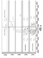
- Figures 5-8 shows waveforms of signals of class-D amplifier 300, according to an embodiment of the present invention.
- FIG. 5 illustrates waveforms in which the duty cycle is increased to a minimum duty cycle (step 408).
- the rising edge of V pwm_out occurs at time t 50 (step 402).
- V pwm_condN transitions from low to high (step 404).
- V pwm_condP transitions from high to low (step 404).
- V pwm_out the next edge
- V out_pre transitions which occurs at time t 55
- the outcome of step 406 is "yes" and both V pwm_condP and V pwm_condN transition at time t 56 , which occurs a time t fix2 +t drv after V pwm_condP transitions from high to low time (which occurs at time t 52 ).
- the reshaped V out_pre signal has a minimum duty cycle, which is longer than the duty cycle that V out_pre would have had without the preconditioning (as illustrated in Figure 5 ).
- the original (lower) duty cycle is not sufficient to cause a full transition of V out_pre (without pre-conditioning).
- FIG. 6 illustrates waveforms in which the duty cycle is decreased to a maximum duty cycle (step 408).
- the falling edge of V pwm_out occurs at time t 60 (step 402).
- V pwm_condP transitions from low to high (step 404).
- V pwm_condN transitions from high to low (step 404).
- time tfixi may be about 8 nS. Other values may also be used.
- V pwm_out the next edge
- V out_pre transitions which occurs at time t 65
- the outcome of step 406 is "yes" and both V pwm_condP and V pwm_condN transition at time t 66 , which occurs a time t fix2 +t drv after V pwm_condP transitions from low to high time (which occurs at time t 62 ).
- the reshaped V out_pre signal has a maximum duty cycle, which is shorter than the duty cycle that V out_pre would have had without the preconditioning (as illustrated in Figure 6 ).
- the original (higher) duty cycle is not sufficient to cause a full transition of V out_pre (without preconditioning).
- Figure 7 illustrates waveforms in which the width of the pulse of PWM signal V pwm_cond is reduced (step 412), during a positive pulse of V pwm_out .
- the rising edge of V pwm_out occurs at time t 70 (step 402).
- V pwm_condN transitions from low to high (step 404).
- V pwm_condP transitions from high to low (step 404).
- V pwm_condN is advanced to transitions at time t 77 , which occurs preset time t fix3 after V pwm_condP transition at time t 76 (step 412).
- a detection signal e.g., V boost_on in this example
- V boost_on causes V pwm_condP to transition at time t 76 .
- the transition of V pwm_condN at time t 77 is controlled by the latch that includes NAND gates 1518 and 1528.
- the reshaped V out_pre positive pulse is shorter that the pulse without the pre-conditioning.
- the time between the V pwm_condN transition and the V pwm_condP transition is lower than t fix1 , which advantageously does not cause X-conduction because of the difference in response times between the high-side transistor (e.g., 106) and low-side transistor (e.g., 108).
- Figure 8 illustrates waveforms in which the width of the pulse of PWM signal V pwm_cond is reduced (step 412), during a negative pulse of V pwm_out .
- the falling edge of V pwm_out occurs at time tso (step 402).
- V pwm_condP transitions from low to high (step 404).
- V pwm_condN transitions from high to low (step 404).
- V pwm_condP is advanced to transitions at time t 87 , which occurs preset time t fix3 after V pwm_condN transition at time t 86 (step 412).
- a detection signal e.g., V slow_off in this example
- V slow_off causes V pwm_condN to transition at time t 86 .
- the transition of V pwm_condP at time t 87 is controlled by the latch that includes NAND gates 1518 and 1528.
- the reshaped V out_pre negative pulse is shorter that the pulse without the pre-conditioning.
- the time between the V pwm_condP transition and the V pwm_condN transition is lower than t fix1 , which advantageously does not cause X-conduction because of the difference in response times between the high-side transistor (e.g., 106) and low-side transistor (e.g., 108).
- Figures 9 and 10 illustrate a comparison between the duty cycles of the voltage V out_pre with pre-conditioning, V out_pre without pre-conditioning, and a reference V out_pre (assuming normal output stage and gate drivers and without pre-conditioning) when operated in open loop (without feedback circuits 308, 314, and 316), according to an embodiment of the present invention.
- the duty cycle approaches 100%, the duty cycle of the pre-conditioned V out_pre is limited (in this embodiment to about 10% duty cycle).
- Figure 10 shows that as the duty cycle approaches 0%, the duty cycle of the pre-conditioned V out_pre is limited (in this embodiment to about 93% duty cycle).
- the duty cycles of the pre-conditioned V out_pre and the V out_pre without conditioning is about identical in the range of about 12% to about 90%.
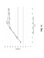
- Figure 11 illustrate simulation results of a comparison between the power consumption of class-D amplifier 300 with pre-conditioning (curve 1102) and without pre-conditioning (curve 1104), according to an embodiment of the present invention.
- pre-conditioning the PWM signal e.g., by using circuit 312 and as illustrated in method 400
- the power savings are caused, in part, by amplifier 300 skipping short pulses when operating in closed loop.
- the clamped duty cycle makes the charge/discharge duration of LC filter 109 fixed when switching near clipping, which makes the feedback loop adjust the output switching frequency automatically to a lower frequency.
- the switching frequency near clipping could be move away from audible band (to a higher frequency) by adjusting the clamped duty cycle level, which in some embodiments, may be implemented by adding a delay to switching detection signals (e.g., V boost_on and V slow_off in Figure 15 ).
- V boost_on and V slow_off in Figure 15 .
- some embodiments advantageously achieve a good compromise between power dissipation and THD, e.g., as illustrated in Figure 11 , 13 , and 14 which may be desirable for high-frequency (HF) class-D amplifiers.
- Figure 12 illustrates Body-Drain diode RMS current of output power of transistors 106 and 108 when implemented as DMOS transistors of the n-type during a transition of V out_pre , according to an embodiment of the present invention.
- some embodiments exhibit a lower BD diode current for the same output power when pre-conditioning the PWM signal, thus advantageously resulting in lower power consumption.
- lowering the power consumption advantageously allows for improved thermal performance of amplifiers in, e.g., integrated solutions.
- pre-conditioning the PWM does not cause a degradation in THD performance.
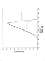
- Figure 13 illustrates simulation results of post-filter output signal V out , and pre-filter output signal V out_pre with and without preconditioning, when amplifier 300 is operated in closed loop, according to an embodiment of the present invention.
- Figure 14 illustrates simulation results of an FFT of the post-filter output signal V out , with and without preconditioning, when amplifier 300 is operated in closed loop, according to an embodiment of the present invention.
- the THD of the non-pre-conditioned output V out is similar to the THD of the pre-conditioned output V out .
- the switching frequency of the pre-conditioned pre-filtered output V out_pre is significantly lower than the non-pre-filtered output V out_pre .
- the duty cycle of V pwn_pre can be adjusted by adding additional delays to switching detection signals (e.g., V boost_on and V slow_off in Figure 15 ) to push the ripple frequency out of audible band.
- Figure 15 shows pre-conditioning circuit 1500, according to an embodiment of the present invention.
- Pre-conditioning circuit 1500 includes pre-conditioning controller 1502, switching status detection circuit 1506, and NAND gates 1518, and 1526.
- Switching status detection circuit 1506 includes comparators 1508 and 1510.
- Pre-conditioning circuit 312 maybe implemented as pre-conditioning circuit 1500.
- Figures 16-19 shows waveforms of signals associated with pre-conditioning circuit 1500, according to an embodiment of the present invention. Figure 15 may be understood together with Figures 16-19 . As can be seen, in some embodiments, Figures 16-19 correspond to Figures 5-8 , respectively.
- pre-conditioning circuit 1500 generates signals V pwm_condP and V pwm_condN to cause gate drive circuit 1504 to drive transistors 106 and 108 to cause signal V out_pre to switch based on signal V pwm_out .
- NAND gates 1518 and 1528 in a latch configuration to prevent X-conduction.
- other implementations for preventing X-conduction may also be used.
- switching status detection circuit 1506 generates detection signals V boost_on and V slow_off based on signal V out_pre .
- comparators 1508 and 1510 which may be implemented with hysteresis, are respectively used to generated signals V boost_on and V slow_off by comparing signal V out_pre with thresholds V th1 and V th2 , respectively, where threshold V th1 is higher than threshold V th2 .
- thresholds V th1 and V th2 may be configurable and may be shifted, e.g., within a predetermined range.
- pre-conditioning controller 1502 is configured to cause a delay (step 408) in signals V pwn_condP and V pwm_condN so that signals V pwm_condP and V pwm_condN switch, e.g., simultaneously, in response to signal V boost_on transitioning from high to low when the duty cycle of V pwm_out is lower than 50%, and when the falling edge of V pwm_out occurs before V out_pre transitions (e.g., before the falling edge of V slow_off ), as illustrated, e.g., in Figure 16 .
- pre-conditioning controller 1502 is configured to cause a delay (step 408) in signals V pwm_condP and V pwm_condN so that signals V pwm_condP and V pwm_condN switch, e.g., simultaneously, in response to signal V slow_off transitioning from low to high when the duty cycle of V pwm_out is higher than 50%, and when the rising edge of V pwm_out occurs before V out_pre transitions (e.g., before the rising edge of V boost_on ), as illustrated, e.g., in Figure 17 .
- pre-conditioning controller 1502 is configured to cause an advance (step 412) in the transitioning of signals V pwm_condN so that signals V pwm_condN and V pwm_condP switch in response to signal V boost_on transitioning from high to low when the duty cycle of V pwm_out is lower than 50%, and when the falling edge of V pwm_out does not occur before V out_pre transitions, as illustrated, e.g., in Figure 18 .
- pre-conditioning controller 1502 is configured to cause an advance (step 412) in the transitioning of signals V pwm_condP so that signals V pwm_condN and V pwm_condP switch in response to signal V slow_off transitioning from low to high when the duty cycle of V pwm_out is higher than 50%, and when the rising edge of V pwm_out does not occur before V out_pre transitions, as illustrated, e.g., in Figure 19 .
- gate drive circuit 1504 may be implemented with inverting gate drivers 1520 and 1526.
- non-inverting gate drivers may also be used instead of inverting gate drivers.
- pre-conditioning controller 1502 generates signals V pwm_condP and V pwm_condN by driving NAND gates 1518 and 1528 with signals V 1512 , V 1516 , V 1530 , and V 1540 .
- Figures 20 shows pre-conditioning controller 2000, according to an embodiment of the present invention.
- Pre-conditioning controller 2000 includes type A pulse generator circuits 2002, 2006, 2014, 2042, 2048, 2052, type B pulse generator circuits 2032 and 2066, type C delay circuits 2070 and 2072, type D delay circuit 2034 and 2056, D-flip-flops 1516, 1530, 2010 and 2044, AND gate 2038, OR gate 2036, 2060 and 2064, and inverters 1512, 1540, 2004, 2008, 2046, 2050, 2054, 2058, and 2062.
- pre-conditioning controller 1502 may be implemented as pre-conditioning controller 2000.
- D-flip-flop 1516 generates signal V 1516 based on V pwm_out and V boost_on
- D-flip-flop 2010 generates signal V 1512 (e.g., via inverter 1512) based on V pwm_out
- D-flip-flop 1530 generates signal V 1530 based on V pwm_out and V slow_off
- D-flip-flop 2044 generates signal V 1540 (e.g., via inverter 1540) based on V pwm_out .
- delay circuits 2070 and 2072 are used to cause delay t fix1 (and t fix2 ), e.g., as illustrated in Figures 5-8 .
- type D delay circuits 2034 and 2056 may be used as filtering logic, e.g., for preventing glitches in the latch that comprises NAND gates 1518 and 1528.
- D-flip-flops 1516, 1530, 2010, and 2044 include a clear input to reset the flip-flop.
- pulse generators 2002, 2006, 2014, 2042, 2048, 2052, 2032 and 2066 are used to set/reset flip-flops 2010, 1516, 2044, and 1530.
- FIGS 21A and 21B illustrate pulse generator circuit 2100 and associated waveforms, respectively, according to an embodiment of the present invention.
- each of type A pulse generator circuits 2002, 2006, 2014, 2042, 2048, 2052 may be implemented as pulse generator circuit 2100.
- FIGs 22A and 22B illustrate pulse generator circuit 2200 and associated waveforms, respectively, according to an embodiment of the present invention.
- each of type B pulse generator circuits 2032 and 2066 may be implemented as pulse generator circuit 2200.
- pulse generator circuits 2100 and 2200 may include identical delay circuits 2102 (e.g., implemented with a plurality of buffers, as shown in Figures 21A and 22A ).
- FIGS 23A and 23B illustrate delay circuit 2300 and associated waveforms, respectively, according to an embodiment of the present invention.
- each of type C delay circuits 2070 and 2072 may be implemented as pulse generator circuit 2300.
- delay circuits 2070 and 2072 may be implemented, instead, with an RC circuit.
- Figures 24A and 24B illustrate delay circuit 2400 and associated waveforms, respectively, according to an embodiment of the present invention.
- type D delay circuits 2034 and 2056 may be implemented as delay circuit 2400.
Landscapes
- Engineering & Computer Science (AREA)
- Power Engineering (AREA)
- Microelectronics & Electronic Packaging (AREA)
- Physics & Mathematics (AREA)
- Acoustics & Sound (AREA)
- Signal Processing (AREA)
- Multimedia (AREA)
- Amplifiers (AREA)
Claims (15)
- Verfahren zur Formung eines Signals mit Impulsbreitenmodulation, PWM, das Verfahren umfassend:Empfangen eines von einer PWM-Modulatorstufe (310) erzeugten Eingangs-PWM-Signals (Vpwm_out) an einem PWM-Eingang einer Vorkonditionierungsschaltung (312, 1500); Ansteuern einer Ausgangsstufe (105) über eine Antriebsschaltung (104, 1504) basierend auf einem konditionierten PWM-Signal (Vpwm_cond), das ein High-Side-(Vpwm_condP) und Low-Side- (Vpwm_condN) zwischengeschaltetes konditioniertes Signal umfasst, wodurch ein Ausgangs-PWM-Signal (Vout_pre) an einem Vorfilterungsknoten der Ausgangsstufe (105) als Ergebnis erzeugt wird,wobei die Ausgangsstufe (105) mit der Antriebsschaltung (104) gekoppelt ist und einen High-Side-Transistor (106) und einen Low-Side-Transistor (108) umfasst, die an den Vorfilterknoten gekoppelt sind, wobei die Treiberschaltung (104) einen High-Side-Gate-Treiber (1520), der mit einem Steueranschluss des High-Side-Transistors (106) gekoppelt ist, und einen Low-Side-Gate-Treiber (1526), der mit einem Steueranschluss des Low-Side-Transistors (108) gekoppelt ist, umfasst, der mittels einer Vorkonditionierungsschaltung (312, 1500) das konditionierte PWM-Signal (Vpwm_cond) basierend auf dem Eingangs-PWM-Signal (Vpwm_out) und dem Ausgangs-PWM-Signal (Vout_pre) , das an einem Schaltungserfassungseingang der Vorkonditionierungsschaltung (312, 1500) empfangen wird, indem,wenn (402) das Eingangs-PWM-Signal (Vpwm_out) mit einer ersten Kante des Eingangs-PWM-Signals (Vpwm_out) umgeschaltet wird, das auf dem Eingangs-PWM-Signal (Vpwm_out) basierende konditionierte PWM-Signal (Vpwm_cond) umgeschaltet wird (404), das seinerseits die Treiberschaltung steuert, sodass die Ausgangsstufe (105) umschaltet, was einen Übergang des Ausgangs-PWM-Signals mit einer ersten Kante des Ausgangs-PWM-Signals (Vout_pre) bewirkt;wenn (406, 408) das Eingangs-PWM-Signal (Vpwm_out) mit einer zweiten Kante umgeschaltet wird, bevor die erste Kante des Ausgangs-PWM-Signals (Vout_pre) umgeschaltet wird, eine zweite Kante des Ausgangs-PWM-Signals verzögert wird, indem eine nächste Kante des bedingten PWM-Signals (Vpwm_cond) basierend auf der ersten Kante des Ausgangs-PWM-Signals (Vout_pre) verzögert wird (tfix1, tfix2, tdrv),wobei die zweite Kante des Eingangs-PWM-Signals (Vpwm_out) eine nächste Kante des Eingangs-PWM-Signals (Vpwm_out) nach der ersten Kante des Eingangs-PWM-Signals (Vpwm_out) ist,wobei die zweite Kante des Ausgangs-PWM-Signals (Vout_pre) eine nächste Kante des Ausgangs-PWM-Signals (Vout_pre) nach der ersten Kante des Ausgangs-PWM-Signals (Vout_pre) ist, undwenn (410, 416) das Eingangs-PWM-Signal (Vpwm_out) mit der zweiten Kante nach der ersten Kante des Ausgangs-PWM-Signals (Vout_pre) umgeschaltet wird, werden basierend auf der ersten Kante des Ausgangs-PWM-Signals (Vout_pre) die High-Side- (Vpwm_condP) und Low-Side- (Vpwm_condN) Zwischensignale im Zustand umgeschaltet (416),wobei das Erzeugen des Ausgangs-PWM-Signals (Vout_pre) das Erzeugen des Ausgangs-PWM-Signals (Vout_pre) mit einem High-Side-Transistor (106) umfasst, der basierend auf dem High-Side-Zwischenzustandssignal (Vpwm_condP) angesteuert wird (1520), und einem Low-Side-Transistor (108), der basierend auf dem Low-Side-Zwischenzustandssignal (Vpwm_condP) angesteuert wird (1526) .
- Verfahren nach Anspruch 1, wobei das Verzögern der zweiten Kante des Ausgangs-PWM-Signals (Vout_pre) das Verzögern der zweiten Kante des Ausgangs-PWM-Signals (Vout_pre) durch Verzögern (408) des konditionierten PWM-Signals (Vpwm_cond) um eine voreingestellte Zeit (tfix2) plus eine Ansteuerverzögerung (tdrv) umfasst, wobei die Ansteuerverzögerung (tdrv) auf einer Verzögerung der Antriebsschaltung (104, 1504) und der Ausgangsstufe (105) basiert.
- Verfahren nach Anspruch 1, ferner umfassend:Vergleichen (1508) des PWM-Ausgangssignals (Vout_pre) mit einem ersten Schwellenwert (Vth1);Vergleichen (1510) des Ausgangs-PWM-Signals (Vout_pre) mit einem zweiten Schwellenwert (Vth2), der sich von dem ersten Schwellenwert (Vth1) unterscheidet; undwenn (408) die zweite Kante des Eingangs-PWM-Signals (Vpwm_out) auftritt, bevor die erste Kante des Ausgangs-PWM-Signals (Vout_pre) den ersten Schwellenwert (Vth1) überschreitet, das Umschalten des konditionierten High-Side-Zwischensignals (Vpwm_condP) und des konditionierten Low-Side-Zwischensignals (Vpwm_condN) verzögert, bis die erste Kante des Ausgangs-PWM-Signals (Vout_pre) den zweiten Schwellenwert (Vth2) überschreitet.
- Verfahren nach Anspruch 3, wobei:
der erste Schwellenwert (Vth1) höher ist als der zweite Schwellenwert (Vth1), und/oder das Umschalten der High-Side (Vpwm_condP) - und Low-Side (Vpwm_condN) - Zwischenkonditionierungssignale das gleichzeitige Umschalten der High-Side (Vpwm_condP) - und Low-Side (Vpwm_condN) -Zwischenkonditionierungssignale umfasst (t56, t66) . - Verfahren nach Anspruch 1, ferner umfassend:Vergleichen (1508) des PWM-Ausgangssignals (Vout_pre) mit einem ersten Schwellenwert (Vth1);Vergleichen (1510) des Ausgangs-PWM-Signals (Vout_pre) mit einem zweiten Schwellenwert (Vth2), der sich von dem ersten Schwellenwert (Vth1) unterscheidet; undwenn (408) die zweite Kante des Eingangs-PWM-Signals (Vpwm_out) auftritt, nachdem die erste Kante des Ausgangs-PWM-Signals (Vout_pre) den ersten Schwellenwert (Vth1) überquert hat, das Umschalten der zwischengeschalteten konditionierten High-Side-(Vpwm_condP) und Low-Side- (Vpwm_condN) Signale, wenn die erste Kante des Ausgangs-PWM-Signals (Vout_pre) den zweiten Schwellenwert (Vth2) überquert.
- Verfahren nach Anspruch 5, wobei:- Umschalten (404) des Ausgangs-PWM-Signals (Vout_pre) mit der ersten Kante das Umschalten der zwischengeschalteten konditionierten High-Side-(Vpwm_condP) und Low-Side- (Vpwm_condN) Signale mit einer voreingestellten Verzögerung (tfix1) dazwischen umfasst, und- wenn (408) die zweite Kante des Eingangs-PWM-Signals (Vpwm_out) auftritt, nachdem die erste Kante des Ausgangs-PWM-Signals (Vout_pre) den ersten Schwellenwert (Vth1) überschritten hat, die High-Side- (Vpwm_condP) und Low-Side- (Vpwm_condN) Zwischensignale mit einer zweiten Verzögerungszeit (tfix3) dazwischen umgeschaltet werden, wobei die zweite Verzögerungszeit (tfix3) kleiner als die voreingestellte Verzögerung (tfix1) ist.
- Verfahren nach Anspruch 1, wobei die erste Kante des PWM-Eingangssignals (Vpwm_out) eine steigende Kante ist, die zweite Kante des PWM-Eingangssignals (Vpwm_out) eine fallende Kante ist, die erste Kante des PWM-Ausgangssignals (Vout_pre) eine steigende Kante ist und die zweite Kante des PWM-Ausgangssignals (Vout_pre) eine fallende Kante ist.
- Verfahren nach Anspruch 1, umfassend:wenn (402) das Eingangs-PWM-Signal (Vpwm_out) mit einer ersten Kante des Eingangs-PWM-Signals (Vpwm_out) umgeschaltet wird, Anlegen der High-Side- (Vpwm_condP) und Low-Side- (Vpwm_condN) Zwischenkonditionierungssignale, um den Übergang (404) des Ausgangs-PWM-Signals (Vout_pre) mit einer ersten Kante des Ausgangs-PWM-Signals (Vout_pre) zu bewirken; undwenn (412) das Eingangs-PWM-Signal (Vpwm_out) mit einer zweiten Kante umgeschaltet wird, nachdem die erste Kante des Ausgangs-PWM-Signals (Vout_pre) umgeschaltet wurde, die auf der ersten Kante des Ausgangs-PWM-Signals (Vout_pre) basierenden konditionierten Zwischensignale (Vpwm_condP) und (Vpwm_condN) umgeschaltet werden, um eine zweite Kante des Ausgangs-PWM-Signals (Vout_pre) zu verursachen, wobei die zweite Kante des Eingangs-PWM-Signals (Vpwm_out) eine nächste Kante des Eingangs-PWM-Signals (Vpwm_out) nach der ersten Kante des Eingangs-PWM-Signals (Vpwm_out) ist, und wobei die zweite Kante des Ausgangs-PWM-Signals (Vout_pre) eine nächste Kante des Ausgangs-PWM-Signals (Vout_pre) nach der ersten Kante des Ausgangs-PWM-Signals (Vout_pre) ist, und das Verfahren ferner umfassend:
wenn (406, 408) das Eingangs-PWM-Signal (Vpwm_out) mit der zweiten Kante umgeschaltet wird, bevor die erste Kante des Ausgangs-PWM-Signals (Vpwm_out) umgeschaltet wird, das Verzögern (tfixl, tfix2, tdrv) der zwischengeschalteten konditionierten Signale auf der High-Seite (Vpwm_condP) und der Low-Seite (Vpwm_condP), um die zweite Kante des Ausgangs-PWM-Signals (Vout_pre) basierend auf der ersten Kante des Ausgangs-PWM-Signals (Vout_pre) zu verzögern. - Impulsbreitenmodulation, PWM-Vorkonditionierungsschaltung (312, 1500), umfassend:einen PWM-Eingang, der so konfiguriert ist, dass er ein von einer PWM-Modulatorstufe (310) erzeugtes Eingangs-PWM-Signal (Vpwm_out) empfängt;High-Side- und Low-Side-Ausgänge, die so konfiguriert sind, dass sie ein High-Side- (Vpwm_condP) bzw. Low-Side- (Vpwm_condP) Zwischenzustandssignal erzeugen, und die so konfiguriert sind, dass sie über eine Steuerungsschaltung (104, 1504, 1520, 1526) mit Terminals von High-Side- (106) und Low-Side- (108) Transistoren gekoppelt werden, zu koppeln, wobei die High-Side- und Low-Side-Transistoren so konfiguriert sind, dass sie angesteuert werden, um basierend auf dem Eingangs-PWM-Signal (Vpwm_out) ein Ausgangs-PWM-Signal (Vout_pre) an einem Vorfilterungsknoten zu erzeugen, an dem der High-Side-Transistor (106) mit dem Low-Side-Transistor (108) gekoppelt ist;einen Schaltfeststellungseingang, der so konfiguriert ist, dass er mit dem Vorfilterungsknoten gekoppelt ist, um das Ausgangs-PWM-Signal (Vout_pre) zu überwachen; undeine Steuerung (1502), konfiguriert zum:wenn (402) das Eingangs-PWM-Signal (Vpwm_out) mit einer ersten Kante des Eingangs-PWM-Signals (Vpwm_out) umschaltet, Ansteuern der High-Side- und Low-Side-Ausgänge, um einen Übergang (404) des Ausgangs-PWM-Signals (Vout_pre) mit einer ersten Kante des Ausgangs-PWM-Signals (Vout_pre) zu verursachen, undwenn (406, 408) das Eingangs-PWM-Signal (Vpwm_out) mit einer zweiten Kante umgeschaltet wird, bevor die erste Kante des Ausgangs-PWM-Signals (Vout_pre) umgeschaltet wird, Ansteuern der High-Side- und Low-Side-Ausgänge zur Verzögerung einer zweiten Kante des Ausgangs-PWM-Signals (Vout_pre) basierend auf der ersten Kante des Ausgangs-PWM-Signals (Vout_pre), wobei die zweite Kante des Eingangs-PWM-Signals (Vpwm_out) eine nächste Kante des Eingangs-PWM-Signals (Vpwm_out) nach der ersten Kante des Eingangs-PWM-Signals (Vpwm_out) ist, und wobei die zweite Kante des Ausgangs-PWM-Signals (Vout_pre) eine nächste Kante des Ausgangs-PWM-Signals (Vout_pre) nach der ersten Kante des Ausgangs-PWM-Signals (Vout_pre) ist,wenn (410, 416) das Eingangs-PWM-Signal (Vpwm_out) mit der zweiten Kante nach der ersten Kante des Ausgangs-PWM-Signals (Vout_pre) umschaltet, das Umschalten (416) der High-Side- (Vpwm_condP) und Low-Side- (Vpwm_condN) zwischenkonditionierten Signale basierend auf der ersten Kante des Ausgangs-PWM-Signals (Vout_pre),wobei das Erzeugen des Ausgangs-PWM-Signals (Vout_pre) das Erzeugen des Ausgangs-PWM-Signals (Vout_pre) mit einem High-Side-Transistor (106), der basierend auf dem High-Side-Zwischenkonditionierungssignal (Vpwm_condP) angesteuert wird (1520), und einem Low-Side-Transistor (108), der basierend auf dem Low-Side-Zwischenkonditionierungssignal (Vpwm_condN) angesteuert wird (1526), umfasst.
- PWM-Vorkonditionierungsschaltung (312, 1500) nach Anspruch 9, die ferner eine Erfassungsschaltung für den Zustand des Schalters (1506) umfasst, umfassend:Einen ersten Komparator (1508) mit einem ersten Eingang, der mit dem Schaltfeststellungseingang gekoppelt ist, und einem zweiten Eingang, der so konfiguriert ist, dass er einen ersten Schwellenwert (Vth1) empfängt; undeinen zweiten Komparator (1510) mit einem ersten Eingang, der mit dem Schaltfeststellungseingang gekoppelt ist, und einem zweiten Eingang, der so konfiguriert ist, dass er einen zweiten Schwellenwert (Vth2) empfängt, der niedriger ist als der erste Schwellenwert (Vth1), wobei die Steuerung (1502) so konfiguriert ist, dass sie basierend auf Ausgängen des ersten (1508) oder zweiten (1510) Komparators bestimmt, ob das Eingangs-PWM-Signal (Vpwm_out) mit einer zweiten Kante vor der ersten Kante des Ausgangs-PWM-Signals (Vout_pre) umgeschaltet wird, und wobei die Steuerung (1502) so konfiguriert ist, dass sie die High-Side- und Low-Side-Ausgänge ansteuert, um die zweite Kante des Ausgangs-PWM-Signals (Vout_pre) basierend auf den Ausgaben des ersten (1508) oder zweiten (1510) Komparators zu verzögern.
- PWM-Vorkonditionierungsschaltung (312, 1500) nach Anspruch 9, ferner umfassend:ein erstes NAND-Gate (1518) mit einem mit dem High-Side-Ausgang gekoppelten Ausgang und einer mit der Steuerung (1502) gekoppelten ersten Eingabe; undein zweites NAND-Gate (1528), das einen Ausgang aufweist, der mit dem Low-Side-Ausgang und mit einem zweiten Eingang des ersten NAND-Gates (1518) gekoppelt ist, einen ersten Eingang, der mit der Steuerung (1502) gekoppelt ist, und einen zweiten Eingang, der mit dem Ausgang des ersten NAND-Gates (1518) gekoppelt ist.
- PWM-Vorkonditionierungsschaltung (312, 1500) nach Anspruch 11, ferner umfassend:ein erstes Flip-Flop (2010), das einen mit dem PWM-Eingang gekoppelten Eingang und einen mit dem ersten Eingang des ersten NAND-Gates (1518) gekoppelten Ausgang aufweist; undein zweites Flip-Flop (1516), das einen ersten Eingang aufweist, der mit dem Ausgang des ersten Flip-Flops (2010) gekoppelt ist, einen zweiten Eingang, der mit dem Schaltfeststellungseingang gekoppelt ist, und einen Ausgang, der mit einem dritten Eingang des ersten NAND-Gates (1518) gekoppelt ist.
- PWM-Vorkonditionierungsschaltung (312, 1500) nach Anspruch 12, ferner umfassend:
eine Erfassungsschaltung für den Schaltzustand (1506), umfassend:einen ersten Komparator (1508) mit einem ersten Eingang, der mit dem Schaltfeststellungseingang gekoppelt ist, und einem zweiten Eingang, der so konfiguriert ist, dass er einen ersten Schwellenwert (Vth1) empfängt, undeinen zweiten Komparator (1510) mit einem ersten Eingang, der mit dem Schaltfeststellungseingang gekoppelt ist, und einem zweiten Eingang, der so konfiguriert ist, dass er einen zweiten Schwellenwert (Vth2) empfängt, der niedriger ist als der erste Schwellenwert (Vth1), wobei der zweite Eingang des zweiten Flip-Flops (1516) mit dem Schaltfeststellungseingang über den ersten Komparator (1508) gekoppelt ist,die Steuerung (1502) ferner umfassend:ein drittes Flip-Flop (2044), das einen mit dem PWM-Eingang gekoppelten Eingang und einen mit dem zweiten Eingang des zweiten NAND-Gatters (1528) gekoppelten Ausgang aufweist; undein viertes Flip-Flop (1530), das einen ersten Eingang aufweist, der mit dem Ausgang des dritten Flip-Flops (2044) gekoppelt ist, einen zweiten Eingang, der mit einem Ausgang des zweiten Komparators (1510) gekoppelt ist, und einen Ausgang, der mit einem dritten Eingang des zweiten NAND-Gatters (1528) gekoppelt ist. - PWM-Vorkonditionierungsschaltung (312, 1500) nach Anspruch 13, wobei die ersten (2010), zweiten (1516), dritten (2044) und vierten (1530) Flip-Flops D-Flip-Flops sind,wobei der erste Eingang des ersten Flip-Flops (2010) ein Takteingang ist,wobei:- der erste Eingang des zweiten Flip-Flops (1516) ein Takteingang ist und der zweite Eingang des zweiten Flip-Flops (1516) ein Löscheingang ist,- der erste Eingang des dritten Flip-Flops (2044) ein Takteingang ist, der erste Eingang des vierten Flip-Flops (1530) ein Takteingang ist, und- der zweite Eingang des vierten Flipflops (1530) ein Löscheingang ist.
- Klasse-D-Verstärker (300), umfassend:Ein Eingangsterminal (302), das zum Empfangen eines analogen Signals (Vin) konfiguriert ist;ein Ausgangsterminal (Vout), das so konfiguriert ist, dass es mit einer Last gekoppelt werden kann;eine Integratorschaltung (304, 306) mit einem ersten Eingang (302), der mit dem Eingangsterminal (Vin) gekoppelt ist, und einem zweiten Eingang (314), der mit dem Ausgangsterminal (Vout) gekoppelt ist;eine Impulsbreitenmodulations-PWM-Modulatorschaltung (310) mit einem ersten Eingang (Vpwm_in), der mit einem Ausgang der Integratorschaltung (304, 306) gekoppelt ist, einem zweiten Eingang (308), der so konfiguriert ist, dass er ein Taktsignal empfängt, und einem Ausgang, der so konfiguriert ist, dass er ein PWM-Eingangssignal (Vpwm_out) liefert;eine PWM-Vorkonditionierungsschaltung (312, 1500) nach einem der Ansprüche 9 bis 14, deren PWM-Eingang mit der PWM-Modulatorschaltung (310) gekoppelt ist und deren Schaltfeststellungseingang (Vout_pre) mit dem Ausgangsterminal (Vout) verbunden ist; undeine Ausgangsstufe (105), die den High-Side-Transistor (106) und den Low-Side-Transistor (108) und den Vorfilterungsknoten als Ausgang umfasst, der mit dem Ausgangsterminal (Vout) gekoppelt ist, wobei die Ausgangsstufe (105) so konfiguriert ist, dass sie das Ausgangs-PWM-Signal (Vout_pre) basierend auf den High-Side- und den Low-Side-Zwischenkonditionierungssignalen durch die PWM-Vorbereitungsschaltung (312, 1500) erzeugt, wobei die Last vorzugsweise ein Audio-Lautsprecher (114) ist.
Applications Claiming Priority (1)
| Application Number | Priority Date | Filing Date | Title |
|---|---|---|---|
| US17/107,269 US11463052B2 (en) | 2020-11-30 | 2020-11-30 | PWM driving circuit and method |
Publications (2)
| Publication Number | Publication Date |
|---|---|
| EP4007166A1 EP4007166A1 (de) | 2022-06-01 |
| EP4007166B1 true EP4007166B1 (de) | 2023-09-20 |
Family
ID=78709185
Family Applications (1)
| Application Number | Title | Priority Date | Filing Date |
|---|---|---|---|
| EP21202997.9A Active EP4007166B1 (de) | 2020-11-30 | 2021-10-15 | Pwm-ansteuerschaltung und -verfahren |
Country Status (3)
| Country | Link |
|---|---|
| US (1) | US11463052B2 (de) |
| EP (1) | EP4007166B1 (de) |
| CN (1) | CN114583949B (de) |
Families Citing this family (1)
| Publication number | Priority date | Publication date | Assignee | Title |
|---|---|---|---|---|
| US11575354B2 (en) * | 2020-08-25 | 2023-02-07 | Rgb Systems, Inc. | Class D amplifier with current mode control |
Family Cites Families (40)
| Publication number | Priority date | Publication date | Assignee | Title |
|---|---|---|---|---|
| US5023566A (en) | 1989-12-21 | 1991-06-11 | General Electric Company | Driver for a high efficiency, high frequency Class-D power amplifier |
| US5247581A (en) * | 1991-09-27 | 1993-09-21 | Exar Corporation | Class-d bicmos hearing aid output amplifier |
| DE69829852T2 (de) | 1998-11-13 | 2006-03-02 | Stmicroelectronics S.R.L., Agrate Brianza | Pulsbreitenmodulierter Brückenverstärker mit konfigurierbarem Eingangsnetzwerk für analogen oder digitalen Eingang ohne Verwendung eines Dreieckwellengenerators |
| KR100809241B1 (ko) | 2000-05-25 | 2008-02-29 | 엔엑스피 비 브이 | 푸쉬-풀 증폭기 및 pwm 리미터 |
| DE60029800T2 (de) | 2000-12-05 | 2007-02-22 | Infineon Technologies Ag | Frequenzbegrenzung und Überlastungsdetektion in einem Spannungsregler |
| FR2829653A1 (fr) | 2001-09-07 | 2003-03-14 | St Microelectronics Sa | Dispositif d'alimentation a decoupage adapte pour les faibles consommations de courant, et telephone cellulaire dote d'un tel dispositif |
| US7142050B2 (en) | 2003-10-15 | 2006-11-28 | Texas Instruments Incorporated | Recovery from clipping events in a class D amplifier |
| US7315202B2 (en) | 2004-07-02 | 2008-01-01 | Yamaha Corporation | Pulse-width modulation amplifier and suppression of clipping therefor |
| EP1843465A1 (de) | 2006-03-29 | 2007-10-10 | STMicroelectronics S.r.l. | Klasse-D Verstärker mit Mehrfach-Rückführung |
| US20070229159A1 (en) | 2006-04-04 | 2007-10-04 | Jagadeesh Krishnan | Multi-mode class-D amplifiers |
| JP2010504004A (ja) | 2006-07-07 | 2010-02-04 | エヌエックスピー ビー ヴィ | D級音声増幅器 |
| US7463089B1 (en) | 2006-07-28 | 2008-12-09 | National Semiconductor Corporation | Class D audio power amplifier for mobile applications |
| US8207788B2 (en) | 2007-04-06 | 2012-06-26 | Avnera Corporation | Calibrated feedback |
| WO2008138163A1 (fr) | 2007-05-09 | 2008-11-20 | Apexone Microelectronics Ltd. | Amplificateur de commutation et son procédé de modulation |
| US7489190B2 (en) * | 2007-07-11 | 2009-02-10 | Himax Analogic, Inc. | Switching audio power amplifier with de-noise function |
| EP2048896B1 (de) | 2007-10-12 | 2011-12-21 | STMicroelectronics Srl | Verfahren und Schaltung zum Testen eines Hochfrequenzlautsprechers eines Lautsprechersystems |
| US7859331B2 (en) * | 2008-05-21 | 2010-12-28 | Silicon Laboratories Inc. | Predictive feedback compensation for PWM switching amplifiers |
| DE102008042377A1 (de) * | 2008-09-25 | 2010-04-01 | Robert Bosch Gmbh | Audioverstärker mit Lastanpassung sowie Verfahren zur Lastanpassung des Audioverstärkers |
| CN101369804B (zh) | 2008-09-27 | 2011-03-23 | 华为技术有限公司 | 消除反馈共模信号的装置和方法 |
| US7795970B2 (en) | 2009-02-11 | 2010-09-14 | Texas Instruments Incorporated | Reduction of dead-time distortion in class D amplifiers |
| JP5196185B2 (ja) | 2009-03-25 | 2013-05-15 | ヤマハ株式会社 | D級増幅回路 |
| US8212612B2 (en) | 2010-07-19 | 2012-07-03 | Broadcom Corporation | Closed-loop class-D amplifier with modulated reference signal and related method |
| JP5578062B2 (ja) | 2010-12-21 | 2014-08-27 | ヤマハ株式会社 | D級増幅回路 |
| US8866544B2 (en) | 2011-04-15 | 2014-10-21 | Fairchild Semiconductor Corporation | Class D pulse width modulator with dual feedback |
| TWI459717B (zh) | 2011-08-01 | 2014-11-01 | Princeton Technology Corp | 放大器電路與調變信號產生電路 |
| US20130089161A1 (en) * | 2011-10-06 | 2013-04-11 | Douglas E. Heineman | Low-Power Modulation in an Amplifier |
| CN104272589B (zh) | 2012-04-30 | 2017-10-24 | 梅鲁斯音频有限公司 | 具有可调环路滤波器特性的d类音频放大器 |
| US8917143B2 (en) | 2012-11-08 | 2014-12-23 | Nuvoton Technology Corporation | Method and apparatus for filter-less analog input class D audio amplifier clipping |
| CN104065353A (zh) | 2013-03-22 | 2014-09-24 | 意法半导体研发(深圳)有限公司 | 静音启动d类放大器 |
| CN104467710B (zh) | 2013-09-12 | 2018-05-04 | 意法半导体研发(深圳)有限公司 | 音频设备中去除pop噪声的方法与电路 |
| US9509261B2 (en) | 2013-12-02 | 2016-11-29 | Crestron Electronics Inc. | Reduced crosstalk and matched output power audio amplifier |
| US9660586B2 (en) | 2014-08-08 | 2017-05-23 | Stmicroelectronics S.R.L. | Class D switching amplifier and method of controlling a loudspeaker |
| CN110048678B (zh) * | 2014-08-29 | 2024-09-27 | 意法半导体研发(深圳)有限公司 | 用于音频放大器的高级电流限制功能 |
| GB2561287B (en) | 2014-08-29 | 2019-03-20 | Cirrus Logic Int Semiconductor Ltd | Class D amplifier circuit |
| US9748940B2 (en) * | 2015-02-09 | 2017-08-29 | Marvell World Trade Ltd. | Pulse width modulation |
| IT201700118558A1 (it) | 2017-10-19 | 2019-04-19 | St Microelectronics Srl | Circuito di modulazione a larghezza di impulso, dispositivo e procedimento corrispondenti |
| US11018644B2 (en) | 2018-11-27 | 2021-05-25 | STMicroelectronics (Shenzen) R&D Co. Ltd. | Audio amplifier with embedded buck controller for class-G application |
| IT201900002953A1 (it) * | 2019-02-28 | 2020-08-28 | St Microelectronics Srl | Circuito rilevatore di clipping di pwm, sistema elettronico e procedimento corrispondenti |
| US10965263B2 (en) | 2019-03-15 | 2021-03-30 | Stmicroelectronics (Shenzhen) R&D Co. Ltd. | Deglitching circuit and method in class-D amplifier |
| US10895601B2 (en) * | 2019-05-10 | 2021-01-19 | Infineon Technologies Ag | System and method of monitoring a switching transistor |
-
2020
- 2020-11-30 US US17/107,269 patent/US11463052B2/en active Active
-
2021
- 2021-10-15 EP EP21202997.9A patent/EP4007166B1/de active Active
- 2021-11-29 CN CN202111430738.8A patent/CN114583949B/zh active Active
Also Published As
| Publication number | Publication date |
|---|---|
| EP4007166A1 (de) | 2022-06-01 |
| CN114583949A (zh) | 2022-06-03 |
| US11463052B2 (en) | 2022-10-04 |
| US20220173706A1 (en) | 2022-06-02 |
| CN114583949B (zh) | 2025-10-03 |
Similar Documents
| Publication | Publication Date | Title |
|---|---|---|
| US10651846B2 (en) | Driver circuit and switching regulator | |
| US7932703B2 (en) | System and method for switch mode power supply delay compensation | |
| US20040232978A1 (en) | Filterless class D amplifiers using spread spectrum PWM modulation | |
| CN101958691B (zh) | D类音频放大器及方法 | |
| US20040027105A1 (en) | Drive apparatus for PWM control of two inductive loads with reduced generation of electrical noise | |
| WO2007020404A9 (en) | Feedback controller for pwm amplifier | |
| US7279965B2 (en) | Reduction of audible artifacts in an audio system | |
| CN109687853B (zh) | 脉冲宽度调制电路、对应的设备和方法 | |
| US20170104462A1 (en) | Method and Apparatus For Achieving Very High-Output Signal Swing From Class-D Amplifier Using Fewer Components | |
| WO2014062832A2 (en) | Glitch suppression in dc-to-dc power conversion | |
| US9847706B2 (en) | Systems and methods for reducing voltage ringing in a power converter | |
| EP4007166B1 (de) | Pwm-ansteuerschaltung und -verfahren | |
| US9124231B2 (en) | Soft turn-off for boost converters | |
| CN107994877A (zh) | 一种低辐射干扰,高效率,线性度高,鲁棒性的d类音频放大器的功率管驱动器 | |
| JP7152642B2 (ja) | デューティサイクル制御を備えるd級アンプ | |
| EP3522373B1 (de) | Ein schaltkreis, entsprechende vorrichtung und verfahren | |
| JP7843816B2 (ja) | スイッチング増幅器における出力ドライバの動的制御 | |
| US7394315B2 (en) | Gate driver for Class D audio amplifier with adaptive dV/dt control | |
| JP4538783B2 (ja) | Dクラスアンプ | |
| CN211670785U (zh) | Llc谐振电路的控制装置及直流-直流转换器 | |
| EP2562933A1 (de) | Verstärker der Klasse D und Steuerverfahren | |
| US20250373231A1 (en) | Adaptive adjustable spread spectrum control circuit and spread spectrum control method thereof | |
| US10985746B1 (en) | Transducer driver enhancement with intelligent threshold selection within non-overlap generator | |
| JP2006101022A (ja) | デジタルアンプ | |
| US8970258B2 (en) | Systems and methods for edge control in a switched output stage |
Legal Events
| Date | Code | Title | Description |
|---|---|---|---|
| PUAI | Public reference made under article 153(3) epc to a published international application that has entered the european phase |
Free format text: ORIGINAL CODE: 0009012 |
|
| STAA | Information on the status of an ep patent application or granted ep patent |
Free format text: STATUS: THE APPLICATION HAS BEEN PUBLISHED |
|
| AK | Designated contracting states |
Kind code of ref document: A1 Designated state(s): AL AT BE BG CH CY CZ DE DK EE ES FI FR GB GR HR HU IE IS IT LI LT LU LV MC MK MT NL NO PL PT RO RS SE SI SK SM TR |
|
| STAA | Information on the status of an ep patent application or granted ep patent |
Free format text: STATUS: REQUEST FOR EXAMINATION WAS MADE |
|
| 17P | Request for examination filed |
Effective date: 20221123 |
|
| RBV | Designated contracting states (corrected) |
Designated state(s): AL AT BE BG CH CY CZ DE DK EE ES FI FR GB GR HR HU IE IS IT LI LT LU LV MC MK MT NL NO PL PT RO RS SE SI SK SM TR |
|
| GRAP | Despatch of communication of intention to grant a patent |
Free format text: ORIGINAL CODE: EPIDOSNIGR1 |
|
| STAA | Information on the status of an ep patent application or granted ep patent |
Free format text: STATUS: GRANT OF PATENT IS INTENDED |
|
| INTG | Intention to grant announced |
Effective date: 20230519 |
|
| GRAS | Grant fee paid |
Free format text: ORIGINAL CODE: EPIDOSNIGR3 |
|
| GRAA | (expected) grant |
Free format text: ORIGINAL CODE: 0009210 |
|
| STAA | Information on the status of an ep patent application or granted ep patent |
Free format text: STATUS: THE PATENT HAS BEEN GRANTED |
|
| AK | Designated contracting states |
Kind code of ref document: B1 Designated state(s): AL AT BE BG CH CY CZ DE DK EE ES FI FR GB GR HR HU IE IS IT LI LT LU LV MC MK MT NL NO PL PT RO RS SE SI SK SM TR |
|
| REG | Reference to a national code |
Ref country code: GB Ref legal event code: FG4D |
|
| REG | Reference to a national code |
Ref country code: CH Ref legal event code: EP |
|
| REG | Reference to a national code |
Ref country code: IE Ref legal event code: FG4D |
|
| REG | Reference to a national code |
Ref country code: DE Ref legal event code: R096 Ref document number: 602021005258 Country of ref document: DE |
|
| REG | Reference to a national code |
Ref country code: LT Ref legal event code: MG9D |
|
| PG25 | Lapsed in a contracting state [announced via postgrant information from national office to epo] |
Ref country code: GR Free format text: LAPSE BECAUSE OF FAILURE TO SUBMIT A TRANSLATION OF THE DESCRIPTION OR TO PAY THE FEE WITHIN THE PRESCRIBED TIME-LIMIT Effective date: 20231221 |
|
| REG | Reference to a national code |
Ref country code: NL Ref legal event code: MP Effective date: 20230920 |
|
| PG25 | Lapsed in a contracting state [announced via postgrant information from national office to epo] |
Ref country code: SE Free format text: LAPSE BECAUSE OF FAILURE TO SUBMIT A TRANSLATION OF THE DESCRIPTION OR TO PAY THE FEE WITHIN THE PRESCRIBED TIME-LIMIT Effective date: 20230920 Ref country code: RS Free format text: LAPSE BECAUSE OF FAILURE TO SUBMIT A TRANSLATION OF THE DESCRIPTION OR TO PAY THE FEE WITHIN THE PRESCRIBED TIME-LIMIT Effective date: 20230920 Ref country code: NO Free format text: LAPSE BECAUSE OF FAILURE TO SUBMIT A TRANSLATION OF THE DESCRIPTION OR TO PAY THE FEE WITHIN THE PRESCRIBED TIME-LIMIT Effective date: 20231220 Ref country code: LV Free format text: LAPSE BECAUSE OF FAILURE TO SUBMIT A TRANSLATION OF THE DESCRIPTION OR TO PAY THE FEE WITHIN THE PRESCRIBED TIME-LIMIT Effective date: 20230920 Ref country code: LT Free format text: LAPSE BECAUSE OF FAILURE TO SUBMIT A TRANSLATION OF THE DESCRIPTION OR TO PAY THE FEE WITHIN THE PRESCRIBED TIME-LIMIT Effective date: 20230920 Ref country code: HR Free format text: LAPSE BECAUSE OF FAILURE TO SUBMIT A TRANSLATION OF THE DESCRIPTION OR TO PAY THE FEE WITHIN THE PRESCRIBED TIME-LIMIT Effective date: 20230920 Ref country code: GR Free format text: LAPSE BECAUSE OF FAILURE TO SUBMIT A TRANSLATION OF THE DESCRIPTION OR TO PAY THE FEE WITHIN THE PRESCRIBED TIME-LIMIT Effective date: 20231221 Ref country code: FI Free format text: LAPSE BECAUSE OF FAILURE TO SUBMIT A TRANSLATION OF THE DESCRIPTION OR TO PAY THE FEE WITHIN THE PRESCRIBED TIME-LIMIT Effective date: 20230920 |
|
| REG | Reference to a national code |
Ref country code: AT Ref legal event code: MK05 Ref document number: 1614194 Country of ref document: AT Kind code of ref document: T Effective date: 20230920 |
|
| PG25 | Lapsed in a contracting state [announced via postgrant information from national office to epo] |
Ref country code: NL Free format text: LAPSE BECAUSE OF FAILURE TO SUBMIT A TRANSLATION OF THE DESCRIPTION OR TO PAY THE FEE WITHIN THE PRESCRIBED TIME-LIMIT Effective date: 20230920 |
|
| PG25 | Lapsed in a contracting state [announced via postgrant information from national office to epo] |
Ref country code: IS Free format text: LAPSE BECAUSE OF FAILURE TO SUBMIT A TRANSLATION OF THE DESCRIPTION OR TO PAY THE FEE WITHIN THE PRESCRIBED TIME-LIMIT Effective date: 20240120 |
|
| PG25 | Lapsed in a contracting state [announced via postgrant information from national office to epo] |
Ref country code: AT Free format text: LAPSE BECAUSE OF FAILURE TO SUBMIT A TRANSLATION OF THE DESCRIPTION OR TO PAY THE FEE WITHIN THE PRESCRIBED TIME-LIMIT Effective date: 20230920 |
|
| PG25 | Lapsed in a contracting state [announced via postgrant information from national office to epo] |
Ref country code: ES Free format text: LAPSE BECAUSE OF FAILURE TO SUBMIT A TRANSLATION OF THE DESCRIPTION OR TO PAY THE FEE WITHIN THE PRESCRIBED TIME-LIMIT Effective date: 20230920 |
|
| PG25 | Lapsed in a contracting state [announced via postgrant information from national office to epo] |
Ref country code: SM Free format text: LAPSE BECAUSE OF FAILURE TO SUBMIT A TRANSLATION OF THE DESCRIPTION OR TO PAY THE FEE WITHIN THE PRESCRIBED TIME-LIMIT Effective date: 20230920 Ref country code: RO Free format text: LAPSE BECAUSE OF FAILURE TO SUBMIT A TRANSLATION OF THE DESCRIPTION OR TO PAY THE FEE WITHIN THE PRESCRIBED TIME-LIMIT Effective date: 20230920 Ref country code: IS Free format text: LAPSE BECAUSE OF FAILURE TO SUBMIT A TRANSLATION OF THE DESCRIPTION OR TO PAY THE FEE WITHIN THE PRESCRIBED TIME-LIMIT Effective date: 20240120 Ref country code: ES Free format text: LAPSE BECAUSE OF FAILURE TO SUBMIT A TRANSLATION OF THE DESCRIPTION OR TO PAY THE FEE WITHIN THE PRESCRIBED TIME-LIMIT Effective date: 20230920 Ref country code: EE Free format text: LAPSE BECAUSE OF FAILURE TO SUBMIT A TRANSLATION OF THE DESCRIPTION OR TO PAY THE FEE WITHIN THE PRESCRIBED TIME-LIMIT Effective date: 20230920 Ref country code: CZ Free format text: LAPSE BECAUSE OF FAILURE TO SUBMIT A TRANSLATION OF THE DESCRIPTION OR TO PAY THE FEE WITHIN THE PRESCRIBED TIME-LIMIT Effective date: 20230920 Ref country code: AT Free format text: LAPSE BECAUSE OF FAILURE TO SUBMIT A TRANSLATION OF THE DESCRIPTION OR TO PAY THE FEE WITHIN THE PRESCRIBED TIME-LIMIT Effective date: 20230920 Ref country code: SK Free format text: LAPSE BECAUSE OF FAILURE TO SUBMIT A TRANSLATION OF THE DESCRIPTION OR TO PAY THE FEE WITHIN THE PRESCRIBED TIME-LIMIT Effective date: 20230920 Ref country code: PT Free format text: LAPSE BECAUSE OF FAILURE TO SUBMIT A TRANSLATION OF THE DESCRIPTION OR TO PAY THE FEE WITHIN THE PRESCRIBED TIME-LIMIT Effective date: 20240122 |
|
| PG25 | Lapsed in a contracting state [announced via postgrant information from national office to epo] |
Ref country code: PL Free format text: LAPSE BECAUSE OF FAILURE TO SUBMIT A TRANSLATION OF THE DESCRIPTION OR TO PAY THE FEE WITHIN THE PRESCRIBED TIME-LIMIT Effective date: 20230920 Ref country code: IT Free format text: LAPSE BECAUSE OF FAILURE TO SUBMIT A TRANSLATION OF THE DESCRIPTION OR TO PAY THE FEE WITHIN THE PRESCRIBED TIME-LIMIT Effective date: 20230920 |
|
| REG | Reference to a national code |
Ref country code: BE Ref legal event code: MM Effective date: 20231031 |
|
| PG25 | Lapsed in a contracting state [announced via postgrant information from national office to epo] |
Ref country code: LU Free format text: LAPSE BECAUSE OF NON-PAYMENT OF DUE FEES Effective date: 20231015 |
|
| REG | Reference to a national code |
Ref country code: DE Ref legal event code: R097 Ref document number: 602021005258 Country of ref document: DE |
|
| PG25 | Lapsed in a contracting state [announced via postgrant information from national office to epo] |
Ref country code: LU Free format text: LAPSE BECAUSE OF NON-PAYMENT OF DUE FEES Effective date: 20231015 |
|
| PG25 | Lapsed in a contracting state [announced via postgrant information from national office to epo] |
Ref country code: MC Free format text: LAPSE BECAUSE OF FAILURE TO SUBMIT A TRANSLATION OF THE DESCRIPTION OR TO PAY THE FEE WITHIN THE PRESCRIBED TIME-LIMIT Effective date: 20230920 |
|
| PG25 | Lapsed in a contracting state [announced via postgrant information from national office to epo] |
Ref country code: DK Free format text: LAPSE BECAUSE OF FAILURE TO SUBMIT A TRANSLATION OF THE DESCRIPTION OR TO PAY THE FEE WITHIN THE PRESCRIBED TIME-LIMIT Effective date: 20230920 |
|
| PLBE | No opposition filed within time limit |
Free format text: ORIGINAL CODE: 0009261 |
|
| STAA | Information on the status of an ep patent application or granted ep patent |
Free format text: STATUS: NO OPPOSITION FILED WITHIN TIME LIMIT |
|
| PG25 | Lapsed in a contracting state [announced via postgrant information from national office to epo] |
Ref country code: MC Free format text: LAPSE BECAUSE OF FAILURE TO SUBMIT A TRANSLATION OF THE DESCRIPTION OR TO PAY THE FEE WITHIN THE PRESCRIBED TIME-LIMIT Effective date: 20230920 Ref country code: DK Free format text: LAPSE BECAUSE OF FAILURE TO SUBMIT A TRANSLATION OF THE DESCRIPTION OR TO PAY THE FEE WITHIN THE PRESCRIBED TIME-LIMIT Effective date: 20230920 |
|
| 26N | No opposition filed |
Effective date: 20240621 |
|
| PG25 | Lapsed in a contracting state [announced via postgrant information from national office to epo] |
Ref country code: BE Free format text: LAPSE BECAUSE OF NON-PAYMENT OF DUE FEES Effective date: 20231031 |
|
| PG25 | Lapsed in a contracting state [announced via postgrant information from national office to epo] |
Ref country code: IE Free format text: LAPSE BECAUSE OF NON-PAYMENT OF DUE FEES Effective date: 20231015 |
|
| PG25 | Lapsed in a contracting state [announced via postgrant information from national office to epo] |
Ref country code: FR Free format text: LAPSE BECAUSE OF NON-PAYMENT OF DUE FEES Effective date: 20231120 |
|
| PG25 | Lapsed in a contracting state [announced via postgrant information from national office to epo] |
Ref country code: SI Free format text: LAPSE BECAUSE OF FAILURE TO SUBMIT A TRANSLATION OF THE DESCRIPTION OR TO PAY THE FEE WITHIN THE PRESCRIBED TIME-LIMIT Effective date: 20230920 |
|
| PG25 | Lapsed in a contracting state [announced via postgrant information from national office to epo] |
Ref country code: SI Free format text: LAPSE BECAUSE OF FAILURE TO SUBMIT A TRANSLATION OF THE DESCRIPTION OR TO PAY THE FEE WITHIN THE PRESCRIBED TIME-LIMIT Effective date: 20230920 Ref country code: IE Free format text: LAPSE BECAUSE OF NON-PAYMENT OF DUE FEES Effective date: 20231015 Ref country code: FR Free format text: LAPSE BECAUSE OF NON-PAYMENT OF DUE FEES Effective date: 20231120 |
|
| PG25 | Lapsed in a contracting state [announced via postgrant information from national office to epo] |
Ref country code: BG Free format text: LAPSE BECAUSE OF FAILURE TO SUBMIT A TRANSLATION OF THE DESCRIPTION OR TO PAY THE FEE WITHIN THE PRESCRIBED TIME-LIMIT Effective date: 20230920 |
|
| PG25 | Lapsed in a contracting state [announced via postgrant information from national office to epo] |
Ref country code: BG Free format text: LAPSE BECAUSE OF FAILURE TO SUBMIT A TRANSLATION OF THE DESCRIPTION OR TO PAY THE FEE WITHIN THE PRESCRIBED TIME-LIMIT Effective date: 20230920 |
|
| REG | Reference to a national code |
Ref country code: CH Ref legal event code: PL |
|
| PG25 | Lapsed in a contracting state [announced via postgrant information from national office to epo] |
Ref country code: CH Free format text: LAPSE BECAUSE OF NON-PAYMENT OF DUE FEES Effective date: 20241031 |
|
| PG25 | Lapsed in a contracting state [announced via postgrant information from national office to epo] |
Ref country code: CY Free format text: LAPSE BECAUSE OF FAILURE TO SUBMIT A TRANSLATION OF THE DESCRIPTION OR TO PAY THE FEE WITHIN THE PRESCRIBED TIME-LIMIT; INVALID AB INITIO Effective date: 20211015 |
|
| PG25 | Lapsed in a contracting state [announced via postgrant information from national office to epo] |
Ref country code: TR Free format text: LAPSE BECAUSE OF FAILURE TO SUBMIT A TRANSLATION OF THE DESCRIPTION OR TO PAY THE FEE WITHIN THE PRESCRIBED TIME-LIMIT Effective date: 20230920 |
|
| PGFP | Annual fee paid to national office [announced via postgrant information from national office to epo] |
Ref country code: DE Payment date: 20250923 Year of fee payment: 5 |
|
| PG25 | Lapsed in a contracting state [announced via postgrant information from national office to epo] |
Ref country code: HU Free format text: LAPSE BECAUSE OF FAILURE TO SUBMIT A TRANSLATION OF THE DESCRIPTION OR TO PAY THE FEE WITHIN THE PRESCRIBED TIME-LIMIT; INVALID AB INITIO Effective date: 20211015 |