EP4007462A1 - Verfahren zur herstellung von stapelkomponenten - Google Patents
Verfahren zur herstellung von stapelkomponenten Download PDFInfo
- Publication number
- EP4007462A1 EP4007462A1 EP19939888.4A EP19939888A EP4007462A1 EP 4007462 A1 EP4007462 A1 EP 4007462A1 EP 19939888 A EP19939888 A EP 19939888A EP 4007462 A1 EP4007462 A1 EP 4007462A1
- Authority
- EP
- European Patent Office
- Prior art keywords
- circuit layer
- circuit
- interposer
- stack component
- manufacturing
- Prior art date
- Legal status (The legal status is an assumption and is not a legal conclusion. Google has not performed a legal analysis and makes no representation as to the accuracy of the status listed.)
- Granted
Links
Images

Classifications
-
- H—ELECTRICITY
- H05—ELECTRIC TECHNIQUES NOT OTHERWISE PROVIDED FOR
- H05K—PRINTED CIRCUITS; CASINGS OR CONSTRUCTIONAL DETAILS OF ELECTRIC APPARATUS; MANUFACTURE OF ASSEMBLAGES OF ELECTRICAL COMPONENTS
- H05K3/00—Apparatus or processes for manufacturing printed circuits
- H05K3/46—Manufacturing multilayer circuits
- H05K3/4697—Manufacturing multilayer circuits having cavities, e.g. for mounting components
-
- B—PERFORMING OPERATIONS; TRANSPORTING
- B33—ADDITIVE MANUFACTURING TECHNOLOGY
- B33Y—ADDITIVE MANUFACTURING, i.e. MANUFACTURING OF THREE-DIMENSIONAL [3D] OBJECTS BY ADDITIVE DEPOSITION, ADDITIVE AGGLOMERATION OR ADDITIVE LAYERING, e.g. BY 3D PRINTING, STEREOLITHOGRAPHY OR SELECTIVE LASER SINTERING
- B33Y10/00—Processes of additive manufacturing
-
- H—ELECTRICITY
- H05—ELECTRIC TECHNIQUES NOT OTHERWISE PROVIDED FOR
- H05K—PRINTED CIRCUITS; CASINGS OR CONSTRUCTIONAL DETAILS OF ELECTRIC APPARATUS; MANUFACTURE OF ASSEMBLAGES OF ELECTRICAL COMPONENTS
- H05K1/00—Printed circuits
- H05K1/02—Details
- H05K1/14—Structural association of two or more printed circuits
- H05K1/144—Stacked arrangements of planar printed circuit boards
-
- H—ELECTRICITY
- H05—ELECTRIC TECHNIQUES NOT OTHERWISE PROVIDED FOR
- H05K—PRINTED CIRCUITS; CASINGS OR CONSTRUCTIONAL DETAILS OF ELECTRIC APPARATUS; MANUFACTURE OF ASSEMBLAGES OF ELECTRICAL COMPONENTS
- H05K3/00—Apparatus or processes for manufacturing printed circuits
- H05K3/10—Apparatus or processes for manufacturing printed circuits in which conductive material is applied to the insulating support in such a manner as to form the desired conductive pattern
-
- H—ELECTRICITY
- H05—ELECTRIC TECHNIQUES NOT OTHERWISE PROVIDED FOR
- H05K—PRINTED CIRCUITS; CASINGS OR CONSTRUCTIONAL DETAILS OF ELECTRIC APPARATUS; MANUFACTURE OF ASSEMBLAGES OF ELECTRICAL COMPONENTS
- H05K3/00—Apparatus or processes for manufacturing printed circuits
- H05K3/46—Manufacturing multilayer circuits
-
- H—ELECTRICITY
- H10—SEMICONDUCTOR DEVICES; ELECTRIC SOLID-STATE DEVICES NOT OTHERWISE PROVIDED FOR
- H10W—GENERIC PACKAGES, INTERCONNECTIONS, CONNECTORS OR OTHER CONSTRUCTIONAL DETAILS OF DEVICES COVERED BY CLASS H10
- H10W90/00—Package configurations
-
- B—PERFORMING OPERATIONS; TRANSPORTING
- B33—ADDITIVE MANUFACTURING TECHNOLOGY
- B33Y—ADDITIVE MANUFACTURING, i.e. MANUFACTURING OF THREE-DIMENSIONAL [3D] OBJECTS BY ADDITIVE DEPOSITION, ADDITIVE AGGLOMERATION OR ADDITIVE LAYERING, e.g. BY 3D PRINTING, STEREOLITHOGRAPHY OR SELECTIVE LASER SINTERING
- B33Y80/00—Products made by additive manufacturing
-
- H—ELECTRICITY
- H05—ELECTRIC TECHNIQUES NOT OTHERWISE PROVIDED FOR
- H05K—PRINTED CIRCUITS; CASINGS OR CONSTRUCTIONAL DETAILS OF ELECTRIC APPARATUS; MANUFACTURE OF ASSEMBLAGES OF ELECTRICAL COMPONENTS
- H05K2201/00—Indexing scheme relating to printed circuits covered by H05K1/00
- H05K2201/03—Conductive materials
- H05K2201/0302—Properties and characteristics in general
- H05K2201/0311—Metallic part with specific elastic properties, e.g. bent piece of metal as electrical contact
-
- H—ELECTRICITY
- H05—ELECTRIC TECHNIQUES NOT OTHERWISE PROVIDED FOR
- H05K—PRINTED CIRCUITS; CASINGS OR CONSTRUCTIONAL DETAILS OF ELECTRIC APPARATUS; MANUFACTURE OF ASSEMBLAGES OF ELECTRICAL COMPONENTS
- H05K2201/00—Indexing scheme relating to printed circuits covered by H05K1/00
- H05K2201/04—Assemblies of printed circuits
- H05K2201/042—Stacked spaced PCBs; Planar parts of folded flexible circuits having mounted components in between or spaced from each other
-
- H—ELECTRICITY
- H05—ELECTRIC TECHNIQUES NOT OTHERWISE PROVIDED FOR
- H05K—PRINTED CIRCUITS; CASINGS OR CONSTRUCTIONAL DETAILS OF ELECTRIC APPARATUS; MANUFACTURE OF ASSEMBLAGES OF ELECTRICAL COMPONENTS
- H05K2201/00—Indexing scheme relating to printed circuits covered by H05K1/00
- H05K2201/10—Details of components or other objects attached to or integrated in a printed circuit board
- H05K2201/10227—Other objects, e.g. metallic pieces
- H05K2201/10295—Metallic connector elements partly mounted in a hole of the PCB
- H05K2201/10303—Pin-in-hole mounted pins
-
- H—ELECTRICITY
- H05—ELECTRIC TECHNIQUES NOT OTHERWISE PROVIDED FOR
- H05K—PRINTED CIRCUITS; CASINGS OR CONSTRUCTIONAL DETAILS OF ELECTRIC APPARATUS; MANUFACTURE OF ASSEMBLAGES OF ELECTRICAL COMPONENTS
- H05K3/00—Apparatus or processes for manufacturing printed circuits
- H05K3/46—Manufacturing multilayer circuits
- H05K3/4688—Composite multilayer circuits, i.e. comprising insulating layers having different properties
- H05K3/4694—Partitioned multilayer circuits having adjacent regions with different properties, e.g. by adding or inserting locally circuit layers having a higher circuit density
-
- H—ELECTRICITY
- H10—SEMICONDUCTOR DEVICES; ELECTRIC SOLID-STATE DEVICES NOT OTHERWISE PROVIDED FOR
- H10W—GENERIC PACKAGES, INTERCONNECTIONS, CONNECTORS OR OTHER CONSTRUCTIONAL DETAILS OF DEVICES COVERED BY CLASS H10
- H10W70/00—Package substrates; Interposers; Redistribution layers [RDL]
- H10W70/60—Insulating or insulated package substrates; Interposers; Redistribution layers
- H10W70/611—Insulating or insulated package substrates; Interposers; Redistribution layers for connecting multiple chips together
- H10W70/614—Insulating or insulated package substrates; Interposers; Redistribution layers for connecting multiple chips together the multiple chips being integrally enclosed
-
- H—ELECTRICITY
- H10—SEMICONDUCTOR DEVICES; ELECTRIC SOLID-STATE DEVICES NOT OTHERWISE PROVIDED FOR
- H10W—GENERIC PACKAGES, INTERCONNECTIONS, CONNECTORS OR OTHER CONSTRUCTIONAL DETAILS OF DEVICES COVERED BY CLASS H10
- H10W70/00—Package substrates; Interposers; Redistribution layers [RDL]
- H10W70/60—Insulating or insulated package substrates; Interposers; Redistribution layers
- H10W70/62—Insulating or insulated package substrates; Interposers; Redistribution layers characterised by their interconnections
- H10W70/63—Vias, e.g. via plugs
-
- H—ELECTRICITY
- H10—SEMICONDUCTOR DEVICES; ELECTRIC SOLID-STATE DEVICES NOT OTHERWISE PROVIDED FOR
- H10W—GENERIC PACKAGES, INTERCONNECTIONS, CONNECTORS OR OTHER CONSTRUCTIONAL DETAILS OF DEVICES COVERED BY CLASS H10
- H10W70/00—Package substrates; Interposers; Redistribution layers [RDL]
- H10W70/60—Insulating or insulated package substrates; Interposers; Redistribution layers
- H10W70/67—Insulating or insulated package substrates; Interposers; Redistribution layers characterised by their insulating layers or insulating parts
- H10W70/68—Shapes or dispositions thereof
- H10W70/682—Shapes or dispositions thereof comprising holes having chips therein
-
- H—ELECTRICITY
- H10—SEMICONDUCTOR DEVICES; ELECTRIC SOLID-STATE DEVICES NOT OTHERWISE PROVIDED FOR
- H10W—GENERIC PACKAGES, INTERCONNECTIONS, CONNECTORS OR OTHER CONSTRUCTIONAL DETAILS OF DEVICES COVERED BY CLASS H10
- H10W72/00—Interconnections or connectors in packages
- H10W72/071—Connecting or disconnecting
- H10W72/072—Connecting or disconnecting of bump connectors
-
- H—ELECTRICITY
- H10—SEMICONDUCTOR DEVICES; ELECTRIC SOLID-STATE DEVICES NOT OTHERWISE PROVIDED FOR
- H10W—GENERIC PACKAGES, INTERCONNECTIONS, CONNECTORS OR OTHER CONSTRUCTIONAL DETAILS OF DEVICES COVERED BY CLASS H10
- H10W72/00—Interconnections or connectors in packages
- H10W72/20—Bump connectors, e.g. solder bumps or copper pillars; Dummy bumps; Thermal bumps
- H10W72/241—Dispositions, e.g. layouts
-
- H—ELECTRICITY
- H10—SEMICONDUCTOR DEVICES; ELECTRIC SOLID-STATE DEVICES NOT OTHERWISE PROVIDED FOR
- H10W—GENERIC PACKAGES, INTERCONNECTIONS, CONNECTORS OR OTHER CONSTRUCTIONAL DETAILS OF DEVICES COVERED BY CLASS H10
- H10W90/00—Package configurations
- H10W90/701—Package configurations characterised by the relative positions of pads or connectors relative to package parts
- H10W90/721—Package configurations characterised by the relative positions of pads or connectors relative to package parts of bump connectors
- H10W90/724—Package configurations characterised by the relative positions of pads or connectors relative to package parts of bump connectors between a chip and a stacked insulating package substrate, interposer or RDL
Definitions
- the present specification discloses a technique related to a method for manufacturing a stack component in which stacked circuit layers are electrically connected by an interlayer connection pin.
- the stack component is manufactured by repeating an operation of using multiple printed circuit boards cut to a predetermined size as multiple circuit layers to be stacked, forming a wiring pattern on each printed circuit board, mounting a circuit element such as a semiconductor chip on each printed circuit board, and thereafter stacking a printed circuit board on an upper layer side via an insulating layer on a printed circuit board on a lower layer side, and inserting an interlayer connection pin into a through hole on the stacked printed circuit board on the upper layer side to electrically connect between two layers of printed circuit boards.
- Patent Literature 1 JP-A-2001-352176
- Patent Literature 1 Since the manufacturing method of Patent Literature 1 described above requires many labor-intensive steps, it has a disadvantage that productivity is poor and a manufacturing cost is high. In addition, since a degree of freedom in design is small, and it is not possible to sufficiently meet the demands for variety and high density of the stacking structure.
- a method for manufacturing a stack component in which a circuit element is mounted on at least one circuit layer of multiple circuit layers to be stacked, the circuit layers are electrically connected by an interlayer connection pin, and an interposer is interposed to form a space for inserting the interlayer connection pin between the circuit layers, the method including: a printing step of simultaneously printing and forming the circuit layer and the interposer side by side in a planar manner by a 3D printer; a step of mounting the circuit element on the circuit layer; a step of mounting the interposer on the circuit layer; a step of inserting the interlayer connection pin into the interposer mounted on the circuit layer; and a step of electrically connecting the circuit layer and another circuit layer by the interlayer connection pin by stacking the other circuit layer on the circuit layer via the interposer.
- a circuit layer and an interposer are simultaneously printed and formed side by side in a planar manner by a 3D printer, and then the interposer is mounted on the circuit layer to assemble the stack component.
- the manufacturing method it is possible to efficiently form the circuit layer and the interposer simultaneously, and it is also easy to diversify the variations of the circuit layer and the interposer.
- the interlayer connection pin is inserted into the interposer mounted on the circuit layer to electrically connect the circuit layers, it is also easy to diversify and increase the density of the stacking structure.
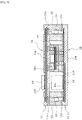
- 3D printer (not illustrated) is used to perform a printing step of simultaneously printing and forming circuit layer 11 and interposer 12 side by side in a planar manner on printing stage 10 on which a print object is mounted.
- Interposer 12 functions as a spacer forming a space (insertion hole) for inserting interlayer connection pin 13 between circuit layers 11 to be stacked.
- At least one circuit layer 11 among multiple circuit layers 11 to be stacked is simultaneously printed with interposer 12 side by side in a planar manner, and, in a case of printing multiple circuit layers 11, multiple circuit layers 11 are simultaneously printed and formed with interposer 12 side by side in a planar manner.
- interposers 12 for multiple layers interposers 12 for multiple layers are simultaneously printed and formed with circuit layers 11 side by side in a planar manner.
- the printing step may be divided into two or more steps.
- some of circuit layers 11 and/or some of interposers 12 may be formed by another forming method.
- Insulating layer 11a is formed by printing insulating ink such as UV resin ink.
- Wiring pattern 11b and terminal section 11c are formed by printing a conductive paste, nanosilver ink, or the like.
- Each interposer 12 is formed by printing insulating ink such as UV resin ink in the same manner as insulating layer 11a.
- circuit element 14 such as a semiconductor chip is mounted at a predetermined position on printed circuit layer 11 by a mounting technique, for example, a surface mounting such as flip-chip bonding, wire bonding, or the like, and thus a terminal of circuit element 14 on a lower surface is connected to terminal section 11c of circuit layer 11.
- a mounting technique for example, a surface mounting such as flip-chip bonding, wire bonding, or the like, and thus a terminal of circuit element 14 on a lower surface is connected to terminal section 11c of circuit layer 11.
- small-sized stack component 21 manufactured by the manufacturing method of the embodiment may be mounted at a predetermined position on circuit layer 11.
- interposer 12 formed on printing stage 10 is peeled from printing stage 10, and interposer 12 is mounted and bonded at a predetermined position on circuit layer 11.
- interlayer connection pin 13 is inserted into interposer 12 mounted on circuit layer 11, and a lower end of interlayer connection pin 13 is electrically connected to terminal section 11c of circuit layer 11.
- Interlayer connection pin 13 used in the embodiment includes a spring (not illustrated), and an upper end portion thereof is configured to be extendable and contractible by the spring. Accordingly, in a state in which interlayer connection pin 13 is inserted into interposer 12, the upper end portion of interlayer connection pin 13 protrudes upward from an upper end of interposer 12.
- unit 15 of the first layer is assembled.
- Units 16 of the second layer and subsequent layers are assembled in the same manner. Thereafter, multiple units 15 and 16 are stacked to manufacture a stack component.
- unit 16 on an upper layer side is stacked on unit 15 on a lower layer side
- circuit layer 11 of unit 16 on the upper layer side is stacked on circuit layer 11 of unit 15 on the lower layer side via interposer 12, and thus circuit layer 11 of unit 15 on the lower layer side and circuit layer 11 of unit 16 on the upper layer side are electrically connected by interlayer connection pin 13.
- the upper end portion of interlayer connection pin 13 contacts and is pushed into terminal section 11c of circuit layer 11 of unit 16 on the upper layer side, so that an electrical connection therebetween is ensured.
- unit 16 on the upper layer side only circuit layer 11 may be stacked.
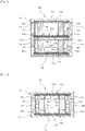
- stack components having various stacking structures illustrated in Figs. 2 to 6 can be assembled.
- a stack component of vertical stacking illustrated in Fig. 2 is a stack component in which two units 15 and 16 are stacked so as to be simply piled up, and only circuit layer 11 on a component surface side is stacked on unit 16 on the upper layer side.
- Units 15, 16 for three or more layers may be vertically stacked, and only circuit layer 11 on the component surface side may be stacked on unit 16 of the uppermost layer.
- a stack component of face-to-face stacking illustrated in Fig. 3 is a stack component in which unit 16 on the upper layer side among two units 15 and 16 is stacked on unit 15 on the lower layer side in a state where unit 16 on the upper layer side is vertically reversed.
- interposer 12 and interlayer connection pin 13 are not mounted, only circuit element 14 is mounted, and circuit layer 11 of unit 16 on the upper layer side is stacked via interposer 12 of unit 15 on the lower layer side.
- the stack component of face-to-face stacking are in a state in which circuit element 14 mounted on circuit layer 11 of unit 16 on the upper layer side is facing downward and is accommodated inside the stack component together with circuit element 14 mounted on circuit layer 11 of unit 15 on the lower layer side.
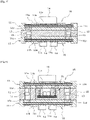
- a stack component of mixed stacking illustrated in Fig. 4 is a stack component in which small-sized stack component 21 assembled by the manufacturing method of the embodiment is mounted with circuit element 14 side by side on circuit layer 11 of unit 15 on the lower layer side, and circuit layer 11 on the component surface side is stacked on unit 15 on the lower layer side.
- Small-sized stack component 21 to be mounted on circuit layer 11 of unit 15 on the lower layer side may be assembled on circuit layer 11 of unit 15 on the lower layer side, or small-sized stack component 21 assembled at another location may be mounted on circuit layer 11 of unit 15 on the lower layer side.
- Circuit element 14 may be mounted on an upper surface of circuit layer 11 on the component surface side.
- a stack component of stacking in a double-sided plate shape illustrated in Fig. 5 is a stack component simulating a double-sided build-up board, in which circuit element 14 is mounted on a lower surface of circuit layer 11 of unit 15 on the lower layer side, and circuit element 14 is mounted on an upper surface of circuit layer 11 on the component surface side stacked on unit 15 on the lower layer side.
- circuit element 14 is mounted on a lower surface of circuit layer 11 of unit 15 on the lower layer side
- circuit element 14 is mounted on an upper surface of circuit layer 11 on the component surface side stacked on unit 15 on the lower layer side.
- interposer 12 and interlayer connection pin 13 are not mounted, only circuit element 14 is mounted, and circuit layer 11 of unit 16 on the upper layer side is stacked via interposer 12 of unit 15 on the lower layer side.
- the step of mounting circuit elements 14 on circuit layers 11 of each unit 15 and 16 may be performed before, or may be performed after the step of stacking two units 15 and 16.
- a stack component of stacking in the double-sided plate shape illustrated in Fig. 6 is a stack component simulating a double-sided build-up board with a built-in component, and have a configuration in which small-sized stack component 21 is built in between layers of the stack component of stacking in the double-sided plate shape.
- Built-in small-sized stack component 21 may be assembled on circuit layer 11 of unit 15 on the lower layer side, or small-sized stack component 21 assembled at another location may be mounted on circuit layer 11 of unit 15 on the lower layer side.
- Other configurations are the same as those of the stack component of stacking in the double-sided plate shape illustrated in Fig. 5 .
- circuit layer 11 and interposer 12 are simultaneously printed and formed side by side in a planar manner on printing stage 10 by using the 3D printer, interposer 12 peeled from printing stage 10 is mounted on circuit layer 11, and unit 15 (16) is assembled by inserting interlayer connection pin 13 into interposer 12. Accordingly, circuit layer 11 and interposer 12 can be simultaneously and efficiently formed, and variations of circuit layer 11 and interposer 12 can be easily diversified.
- unit 15 (16) for one layer is configured by inserting interlayer connection pin 13 into interposer 12 mounted on circuit layer 11, it is possible to manufacture stack components having various stacking structures illustrated in Figs. 2 to 6 , and it is also easy to diversify and increase the density of the stacking structure.
- the present invention is not limited to the configuration of the above embodiment, and can be implemented with various changes within the range not departing from the gist, such as changing the number of stacks of circuit layers 11 and the number of circuit elements 14 to be mounted, or using interlayer connection pin with no built-in spring.
Landscapes
- Engineering & Computer Science (AREA)
- Manufacturing & Machinery (AREA)
- Microelectronics & Electronic Packaging (AREA)
- Chemical & Material Sciences (AREA)
- Materials Engineering (AREA)
- Production Of Multi-Layered Print Wiring Board (AREA)
- Printing Elements For Providing Electric Connections Between Printed Circuits (AREA)
Applications Claiming Priority (1)
| Application Number | Priority Date | Filing Date | Title |
|---|---|---|---|
| PCT/JP2019/029821 WO2021019684A1 (ja) | 2019-07-30 | 2019-07-30 | スタック部品の製造方法 |
Publications (3)
| Publication Number | Publication Date |
|---|---|
| EP4007462A1 true EP4007462A1 (de) | 2022-06-01 |
| EP4007462A4 EP4007462A4 (de) | 2022-08-24 |
| EP4007462B1 EP4007462B1 (de) | 2026-01-14 |
Family
ID=74228358
Family Applications (1)
| Application Number | Title | Priority Date | Filing Date |
|---|---|---|---|
| EP19939888.4A Active EP4007462B1 (de) | 2019-07-30 | 2019-07-30 | Verfahren zur herstellung von stapelkomponenten |
Country Status (4)
| Country | Link |
|---|---|
| US (1) | US12119327B2 (de) |
| EP (1) | EP4007462B1 (de) |
| JP (1) | JP7130875B2 (de) |
| WO (1) | WO2021019684A1 (de) |
Families Citing this family (2)
| Publication number | Priority date | Publication date | Assignee | Title |
|---|---|---|---|---|
| JP7529152B2 (ja) * | 2021-05-18 | 2024-08-06 | 富士電機株式会社 | 半導体装置及び半導体装置の製造方法 |
| WO2024018615A1 (ja) * | 2022-07-22 | 2024-01-25 | 株式会社Fuji | インタポーザ部材、回路基板作製方法、および設計方法 |
Family Cites Families (7)
| Publication number | Priority date | Publication date | Assignee | Title |
|---|---|---|---|---|
| JPH07193350A (ja) | 1993-12-27 | 1995-07-28 | Kokusai Electric Co Ltd | 高周波信号の接続装置 |
| JP2001352176A (ja) | 2000-06-05 | 2001-12-21 | Fuji Xerox Co Ltd | 多層プリント配線基板および多層プリント配線基板製造方法 |
| JP4888073B2 (ja) * | 2006-11-16 | 2012-02-29 | セイコーエプソン株式会社 | 電子基板の製造方法 |
| JP4424449B2 (ja) | 2007-05-02 | 2010-03-03 | 株式会社村田製作所 | 部品内蔵モジュール及びその製造方法 |
| JP2017130553A (ja) * | 2016-01-20 | 2017-07-27 | 株式会社ミマキエンジニアリング | 電子素子設置基材の製造方法、電子部材の製造方法、及び造形装置 |
| JP6811770B2 (ja) * | 2016-06-08 | 2021-01-13 | 株式会社Fuji | 回路形成方法 |
| WO2019102522A1 (ja) * | 2017-11-21 | 2019-05-31 | 株式会社Fuji | 3次元積層電子デバイスの製造方法及び3次元積層電子デバイス |
-
2019
- 2019-07-30 JP JP2021536514A patent/JP7130875B2/ja active Active
- 2019-07-30 WO PCT/JP2019/029821 patent/WO2021019684A1/ja not_active Ceased
- 2019-07-30 US US17/630,870 patent/US12119327B2/en active Active
- 2019-07-30 EP EP19939888.4A patent/EP4007462B1/de active Active
Also Published As
| Publication number | Publication date |
|---|---|
| US20220271010A1 (en) | 2022-08-25 |
| JP7130875B2 (ja) | 2022-09-05 |
| US12119327B2 (en) | 2024-10-15 |
| EP4007462A4 (de) | 2022-08-24 |
| JPWO2021019684A1 (de) | 2021-02-04 |
| EP4007462B1 (de) | 2026-01-14 |
| WO2021019684A1 (ja) | 2021-02-04 |
Similar Documents
| Publication | Publication Date | Title |
|---|---|---|
| KR101084252B1 (ko) | 전자소자 내장형 인쇄회로기판 및 그 제조방법 | |
| US8963013B2 (en) | Three dimensional interposer device | |
| US20120018193A1 (en) | Multi layer circuit board and method of manufacturing the same | |
| CN108140968B (zh) | 具有转接装置的连接器系统 | |
| EP3032655A1 (de) | Trennbare elektrische verbindungsstruktur und verbinder für elektrische verbindungen damit, halbleitergehäuseanordnung und elektronische vorrichtung | |
| KR20100106938A (ko) | 소켓과 헤더의 결합 상태를 유지하는 록 기구를 구비한 커넥터 및 커넥터의 제조 방법 | |
| KR101689547B1 (ko) | 전기 접속 구조의 제조 방법 | |
| US20100097770A1 (en) | Printed circuit board and manufacturing method thereof | |
| CN108353500B (zh) | 基板装置及制造基板装置的方法 | |
| US20160270222A1 (en) | Multilayer wiring board and probe card having the same | |
| EP4007462B1 (de) | Verfahren zur herstellung von stapelkomponenten | |
| US20130058032A1 (en) | Portable data storage devices and hosts compliant with multiple communications standards | |
| KR101689546B1 (ko) | 착탈형 전기 접속 구조와 이를 구비하는 전자기기 | |
| EP2849226B1 (de) | Halbleiterpaket | |
| CN100492680C (zh) | 多层表面安装发光二极管 | |
| JP4033157B2 (ja) | 導電路形成方法 | |
| CN101257767A (zh) | 印刷电路板及其制造方法 | |
| JP2010114074A (ja) | 基板挿入用コネクタ及びその製造方法 | |
| US20150380347A1 (en) | Semiconductor device and method of manufacturing semiconductor device | |
| CN214542186U (zh) | 封装芯片和移动终端 | |
| US8304895B2 (en) | Semiconductor package and method of fabricating the same | |
| JP4746376B2 (ja) | セラミック多層基板及びその製造方法 | |
| JP3189807U (ja) | コネクタ及びコネクタ装置 | |
| KR101251660B1 (ko) | 인쇄회로기판과 인쇄회로기판을 이용한 피씨비 카드,그리고 인쇄회로기판의 제조방법 및 pcb 카드의제조방법 | |
| JP2001053217A (ja) | 三次元半導体装置用スタックキャリアおよび三次元半導体装置 |
Legal Events
| Date | Code | Title | Description |
|---|---|---|---|
| STAA | Information on the status of an ep patent application or granted ep patent |
Free format text: STATUS: THE INTERNATIONAL PUBLICATION HAS BEEN MADE |
|
| PUAI | Public reference made under article 153(3) epc to a published international application that has entered the european phase |
Free format text: ORIGINAL CODE: 0009012 |
|
| STAA | Information on the status of an ep patent application or granted ep patent |
Free format text: STATUS: REQUEST FOR EXAMINATION WAS MADE |
|
| 17P | Request for examination filed |
Effective date: 20220105 |
|
| AK | Designated contracting states |
Kind code of ref document: A1 Designated state(s): AL AT BE BG CH CY CZ DE DK EE ES FI FR GB GR HR HU IE IS IT LI LT LU LV MC MK MT NL NO PL PT RO RS SE SI SK SM TR |
|
| A4 | Supplementary search report drawn up and despatched |
Effective date: 20220725 |
|
| RIC1 | Information provided on ipc code assigned before grant |
Ipc: B33Y 80/00 20150101ALN20220719BHEP Ipc: B33Y 10/00 20150101ALN20220719BHEP Ipc: H05K 1/14 20060101ALI20220719BHEP Ipc: H05K 3/46 20060101AFI20220719BHEP |
|
| DAV | Request for validation of the european patent (deleted) | ||
| DAX | Request for extension of the european patent (deleted) | ||
| P01 | Opt-out of the competence of the unified patent court (upc) registered |
Effective date: 20230328 |
|
| GRAP | Despatch of communication of intention to grant a patent |
Free format text: ORIGINAL CODE: EPIDOSNIGR1 |
|
| STAA | Information on the status of an ep patent application or granted ep patent |
Free format text: STATUS: GRANT OF PATENT IS INTENDED |
|
| RIC1 | Information provided on ipc code assigned before grant |
Ipc: H05K 3/46 20060101AFI20250903BHEP Ipc: H05K 1/14 20060101ALI20250903BHEP Ipc: B33Y 10/00 20150101ALN20250903BHEP Ipc: B33Y 80/00 20150101ALN20250903BHEP |
|
| INTG | Intention to grant announced |
Effective date: 20250917 |
|
| GRAS | Grant fee paid |
Free format text: ORIGINAL CODE: EPIDOSNIGR3 |
|
| GRAA | (expected) grant |
Free format text: ORIGINAL CODE: 0009210 |
|
| STAA | Information on the status of an ep patent application or granted ep patent |
Free format text: STATUS: THE PATENT HAS BEEN GRANTED |
|
| AK | Designated contracting states |
Kind code of ref document: B1 Designated state(s): AL AT BE BG CH CY CZ DE DK EE ES FI FR GB GR HR HU IE IS IT LI LT LU LV MC MK MT NL NO PL PT RO RS SE SI SK SM TR |
|
| REG | Reference to a national code |
Ref country code: CH Ref legal event code: F10 Free format text: ST27 STATUS EVENT CODE: U-0-0-F10-F00 (AS PROVIDED BY THE NATIONAL OFFICE) Effective date: 20260114 Ref country code: GB Ref legal event code: FG4D |
|
| REG | Reference to a national code |
Ref country code: DE Ref legal event code: R096 Ref document number: 602019080487 Country of ref document: DE |
|
| REG | Reference to a national code |
Ref country code: IE Ref legal event code: FG4D |