EP4009315B1 - Appareil d'affichage et son dispositif d'éclairage - Google Patents
Appareil d'affichage et son dispositif d'éclairage Download PDFInfo
- Publication number
- EP4009315B1 EP4009315B1 EP21194729.6A EP21194729A EP4009315B1 EP 4009315 B1 EP4009315 B1 EP 4009315B1 EP 21194729 A EP21194729 A EP 21194729A EP 4009315 B1 EP4009315 B1 EP 4009315B1
- Authority
- EP
- European Patent Office
- Prior art keywords
- driving
- dimming
- area
- driving device
- light
- Prior art date
- Legal status (The legal status is an assumption and is not a legal conclusion. Google has not performed a legal analysis and makes no representation as to the accuracy of the status listed.)
- Active
Links
Images








Classifications
-
- H—ELECTRICITY
- H10—SEMICONDUCTOR DEVICES; ELECTRIC SOLID-STATE DEVICES NOT OTHERWISE PROVIDED FOR
- H10W—GENERIC PACKAGES, INTERCONNECTIONS, CONNECTORS OR OTHER CONSTRUCTIONAL DETAILS OF DEVICES COVERED BY CLASS H10
- H10W90/00—Package configurations
-
- G—PHYSICS
- G09—EDUCATION; CRYPTOGRAPHY; DISPLAY; ADVERTISING; SEALS
- G09G—ARRANGEMENTS OR CIRCUITS FOR CONTROL OF INDICATING DEVICES USING STATIC MEANS TO PRESENT VARIABLE INFORMATION
- G09G3/00—Control arrangements or circuits, of interest only in connection with visual indicators other than cathode-ray tubes
- G09G3/20—Control arrangements or circuits, of interest only in connection with visual indicators other than cathode-ray tubes for presentation of an assembly of a number of characters, e.g. a page, by composing the assembly by combination of individual elements arranged in a matrix no fixed position being assigned to or needed to be assigned to the individual characters or partial characters
- G09G3/34—Control arrangements or circuits, of interest only in connection with visual indicators other than cathode-ray tubes for presentation of an assembly of a number of characters, e.g. a page, by composing the assembly by combination of individual elements arranged in a matrix no fixed position being assigned to or needed to be assigned to the individual characters or partial characters by control of light from an independent source
- G09G3/36—Control arrangements or circuits, of interest only in connection with visual indicators other than cathode-ray tubes for presentation of an assembly of a number of characters, e.g. a page, by composing the assembly by combination of individual elements arranged in a matrix no fixed position being assigned to or needed to be assigned to the individual characters or partial characters by control of light from an independent source using liquid crystals
- G09G3/3611—Control of matrices with row and column drivers
- G09G3/3648—Control of matrices with row and column drivers using an active matrix
-
- G—PHYSICS
- G02—OPTICS
- G02F—OPTICAL DEVICES OR ARRANGEMENTS FOR THE CONTROL OF LIGHT BY MODIFICATION OF THE OPTICAL PROPERTIES OF THE MEDIA OF THE ELEMENTS INVOLVED THEREIN; NON-LINEAR OPTICS; FREQUENCY-CHANGING OF LIGHT; OPTICAL LOGIC ELEMENTS; OPTICAL ANALOGUE/DIGITAL CONVERTERS
- G02F1/00—Devices or arrangements for the control of the intensity, colour, phase, polarisation or direction of light arriving from an independent light source, e.g. switching, gating or modulating; Non-linear optics
- G02F1/01—Devices or arrangements for the control of the intensity, colour, phase, polarisation or direction of light arriving from an independent light source, e.g. switching, gating or modulating; Non-linear optics for the control of the intensity, phase, polarisation or colour
- G02F1/13—Devices or arrangements for the control of the intensity, colour, phase, polarisation or direction of light arriving from an independent light source, e.g. switching, gating or modulating; Non-linear optics for the control of the intensity, phase, polarisation or colour based on liquid crystals, e.g. single liquid crystal display cells
- G02F1/133—Constructional arrangements; Operation of liquid crystal cells; Circuit arrangements
- G02F1/1333—Constructional arrangements; Manufacturing methods
- G02F1/1335—Structural association of cells with optical devices, e.g. polarisers or reflectors
- G02F1/1336—Illuminating devices
- G02F1/133602—Direct backlight
- G02F1/133603—Direct backlight with LEDs
-
- G—PHYSICS
- G09—EDUCATION; CRYPTOGRAPHY; DISPLAY; ADVERTISING; SEALS
- G09G—ARRANGEMENTS OR CIRCUITS FOR CONTROL OF INDICATING DEVICES USING STATIC MEANS TO PRESENT VARIABLE INFORMATION
- G09G3/00—Control arrangements or circuits, of interest only in connection with visual indicators other than cathode-ray tubes
- G09G3/20—Control arrangements or circuits, of interest only in connection with visual indicators other than cathode-ray tubes for presentation of an assembly of a number of characters, e.g. a page, by composing the assembly by combination of individual elements arranged in a matrix no fixed position being assigned to or needed to be assigned to the individual characters or partial characters
- G09G3/22—Control arrangements or circuits, of interest only in connection with visual indicators other than cathode-ray tubes for presentation of an assembly of a number of characters, e.g. a page, by composing the assembly by combination of individual elements arranged in a matrix no fixed position being assigned to or needed to be assigned to the individual characters or partial characters using controlled light sources
- G09G3/30—Control arrangements or circuits, of interest only in connection with visual indicators other than cathode-ray tubes for presentation of an assembly of a number of characters, e.g. a page, by composing the assembly by combination of individual elements arranged in a matrix no fixed position being assigned to or needed to be assigned to the individual characters or partial characters using controlled light sources using electroluminescent panels
- G09G3/32—Control arrangements or circuits, of interest only in connection with visual indicators other than cathode-ray tubes for presentation of an assembly of a number of characters, e.g. a page, by composing the assembly by combination of individual elements arranged in a matrix no fixed position being assigned to or needed to be assigned to the individual characters or partial characters using controlled light sources using electroluminescent panels semiconductive, e.g. using light-emitting diodes [LED]
-
- G—PHYSICS
- G09—EDUCATION; CRYPTOGRAPHY; DISPLAY; ADVERTISING; SEALS
- G09G—ARRANGEMENTS OR CIRCUITS FOR CONTROL OF INDICATING DEVICES USING STATIC MEANS TO PRESENT VARIABLE INFORMATION
- G09G3/00—Control arrangements or circuits, of interest only in connection with visual indicators other than cathode-ray tubes
- G09G3/20—Control arrangements or circuits, of interest only in connection with visual indicators other than cathode-ray tubes for presentation of an assembly of a number of characters, e.g. a page, by composing the assembly by combination of individual elements arranged in a matrix no fixed position being assigned to or needed to be assigned to the individual characters or partial characters
- G09G3/34—Control arrangements or circuits, of interest only in connection with visual indicators other than cathode-ray tubes for presentation of an assembly of a number of characters, e.g. a page, by composing the assembly by combination of individual elements arranged in a matrix no fixed position being assigned to or needed to be assigned to the individual characters or partial characters by control of light from an independent source
- G09G3/3406—Control of illumination source
- G09G3/342—Control of illumination source using several illumination sources separately controlled corresponding to different display panel areas, e.g. along one dimension such as lines
- G09G3/3426—Control of illumination source using several illumination sources separately controlled corresponding to different display panel areas, e.g. along one dimension such as lines the different display panel areas being distributed in two dimensions, e.g. matrix
-
- H—ELECTRICITY
- H10—SEMICONDUCTOR DEVICES; ELECTRIC SOLID-STATE DEVICES NOT OTHERWISE PROVIDED FOR
- H10H—INORGANIC LIGHT-EMITTING SEMICONDUCTOR DEVICES HAVING POTENTIAL BARRIERS
- H10H20/00—Individual inorganic light-emitting semiconductor devices having potential barriers, e.g. light-emitting diodes [LED]
- H10H20/80—Constructional details
- H10H20/81—Bodies
- H10H20/814—Bodies having reflecting means, e.g. semiconductor Bragg reflectors
-
- H—ELECTRICITY
- H10—SEMICONDUCTOR DEVICES; ELECTRIC SOLID-STATE DEVICES NOT OTHERWISE PROVIDED FOR
- H10H—INORGANIC LIGHT-EMITTING SEMICONDUCTOR DEVICES HAVING POTENTIAL BARRIERS
- H10H20/00—Individual inorganic light-emitting semiconductor devices having potential barriers, e.g. light-emitting diodes [LED]
- H10H20/80—Constructional details
- H10H20/84—Coatings, e.g. passivation layers or antireflective coatings
- H10H20/841—Reflective coatings, e.g. dielectric Bragg reflectors
-
- H—ELECTRICITY
- H10—SEMICONDUCTOR DEVICES; ELECTRIC SOLID-STATE DEVICES NOT OTHERWISE PROVIDED FOR
- H10H—INORGANIC LIGHT-EMITTING SEMICONDUCTOR DEVICES HAVING POTENTIAL BARRIERS
- H10H20/00—Individual inorganic light-emitting semiconductor devices having potential barriers, e.g. light-emitting diodes [LED]
- H10H20/80—Constructional details
- H10H20/85—Packages
- H10H20/852—Encapsulations
-
- H—ELECTRICITY
- H10—SEMICONDUCTOR DEVICES; ELECTRIC SOLID-STATE DEVICES NOT OTHERWISE PROVIDED FOR
- H10H—INORGANIC LIGHT-EMITTING SEMICONDUCTOR DEVICES HAVING POTENTIAL BARRIERS
- H10H20/00—Individual inorganic light-emitting semiconductor devices having potential barriers, e.g. light-emitting diodes [LED]
- H10H20/80—Constructional details
- H10H20/85—Packages
- H10H20/852—Encapsulations
- H10H20/853—Encapsulations characterised by their shape
-
- H—ELECTRICITY
- H10—SEMICONDUCTOR DEVICES; ELECTRIC SOLID-STATE DEVICES NOT OTHERWISE PROVIDED FOR
- H10H—INORGANIC LIGHT-EMITTING SEMICONDUCTOR DEVICES HAVING POTENTIAL BARRIERS
- H10H20/00—Individual inorganic light-emitting semiconductor devices having potential barriers, e.g. light-emitting diodes [LED]
- H10H20/80—Constructional details
- H10H20/85—Packages
- H10H20/855—Optical field-shaping means, e.g. lenses
-
- G—PHYSICS
- G02—OPTICS
- G02F—OPTICAL DEVICES OR ARRANGEMENTS FOR THE CONTROL OF LIGHT BY MODIFICATION OF THE OPTICAL PROPERTIES OF THE MEDIA OF THE ELEMENTS INVOLVED THEREIN; NON-LINEAR OPTICS; FREQUENCY-CHANGING OF LIGHT; OPTICAL LOGIC ELEMENTS; OPTICAL ANALOGUE/DIGITAL CONVERTERS
- G02F2201/00—Constructional arrangements not provided for in groups G02F1/00 - G02F7/00
- G02F2201/34—Constructional arrangements not provided for in groups G02F1/00 - G02F7/00 reflector
- G02F2201/346—Constructional arrangements not provided for in groups G02F1/00 - G02F7/00 reflector distributed (Bragg) reflector
-
- G—PHYSICS
- G09—EDUCATION; CRYPTOGRAPHY; DISPLAY; ADVERTISING; SEALS
- G09G—ARRANGEMENTS OR CIRCUITS FOR CONTROL OF INDICATING DEVICES USING STATIC MEANS TO PRESENT VARIABLE INFORMATION
- G09G2300/00—Aspects of the constitution of display devices
- G09G2300/02—Composition of display devices
- G09G2300/023—Display panel composed of stacked panels
-
- G—PHYSICS
- G09—EDUCATION; CRYPTOGRAPHY; DISPLAY; ADVERTISING; SEALS
- G09G—ARRANGEMENTS OR CIRCUITS FOR CONTROL OF INDICATING DEVICES USING STATIC MEANS TO PRESENT VARIABLE INFORMATION
- G09G2300/00—Aspects of the constitution of display devices
- G09G2300/04—Structural and physical details of display devices
- G09G2300/0404—Matrix technologies
- G09G2300/0408—Integration of the drivers onto the display substrate
-
- G—PHYSICS
- G09—EDUCATION; CRYPTOGRAPHY; DISPLAY; ADVERTISING; SEALS
- G09G—ARRANGEMENTS OR CIRCUITS FOR CONTROL OF INDICATING DEVICES USING STATIC MEANS TO PRESENT VARIABLE INFORMATION
- G09G2300/00—Aspects of the constitution of display devices
- G09G2300/04—Structural and physical details of display devices
- G09G2300/0421—Structural details of the set of electrodes
- G09G2300/0426—Layout of electrodes and connections
-
- G—PHYSICS
- G09—EDUCATION; CRYPTOGRAPHY; DISPLAY; ADVERTISING; SEALS
- G09G—ARRANGEMENTS OR CIRCUITS FOR CONTROL OF INDICATING DEVICES USING STATIC MEANS TO PRESENT VARIABLE INFORMATION
- G09G2300/00—Aspects of the constitution of display devices
- G09G2300/08—Active matrix structure, i.e. with use of active elements, inclusive of non-linear two terminal elements, in the pixels together with light emitting or modulating elements
- G09G2300/0804—Sub-multiplexed active matrix panel, i.e. wherein one active driving circuit is used at pixel level for multiple image producing elements
-
- G—PHYSICS
- G09—EDUCATION; CRYPTOGRAPHY; DISPLAY; ADVERTISING; SEALS
- G09G—ARRANGEMENTS OR CIRCUITS FOR CONTROL OF INDICATING DEVICES USING STATIC MEANS TO PRESENT VARIABLE INFORMATION
- G09G2320/00—Control of display operating conditions
- G09G2320/02—Improving the quality of display appearance
- G09G2320/0233—Improving the luminance or brightness uniformity across the screen
-
- G—PHYSICS
- G09—EDUCATION; CRYPTOGRAPHY; DISPLAY; ADVERTISING; SEALS
- G09G—ARRANGEMENTS OR CIRCUITS FOR CONTROL OF INDICATING DEVICES USING STATIC MEANS TO PRESENT VARIABLE INFORMATION
- G09G3/00—Control arrangements or circuits, of interest only in connection with visual indicators other than cathode-ray tubes
- G09G3/20—Control arrangements or circuits, of interest only in connection with visual indicators other than cathode-ray tubes for presentation of an assembly of a number of characters, e.g. a page, by composing the assembly by combination of individual elements arranged in a matrix no fixed position being assigned to or needed to be assigned to the individual characters or partial characters
- G09G3/2085—Special arrangements for addressing the individual elements of the matrix, other than by driving respective rows and columns in combination
- G09G3/2088—Special arrangements for addressing the individual elements of the matrix, other than by driving respective rows and columns in combination with use of a plurality of processors, each processor controlling a number of individual elements of the matrix
-
- H—ELECTRICITY
- H10—SEMICONDUCTOR DEVICES; ELECTRIC SOLID-STATE DEVICES NOT OTHERWISE PROVIDED FOR
- H10H—INORGANIC LIGHT-EMITTING SEMICONDUCTOR DEVICES HAVING POTENTIAL BARRIERS
- H10H20/00—Individual inorganic light-emitting semiconductor devices having potential barriers, e.g. light-emitting diodes [LED]
- H10H20/80—Constructional details
- H10H20/85—Packages
- H10H20/857—Interconnections, e.g. lead-frames, bond wires or solder balls
Definitions
- the disclosure relates to a display apparatus and a light apparatus thereof, and more particularly, to a thin display apparatus and a light source module thereof.
- display apparatuses are a type of output devices for displaying obtained or stored electrical information for the user by converting the electrical information to visual information.
- Display apparatuses are used in various fields such as homes or work places.
- PCs personal computers
- server computers portable computer systems
- GPS Global Positioning System
- IPTVs Internet protocol televisions
- portable terminals e.g., smart phones, tablet PCs, personal digital assistants (PDAs), and cellular phones
- display devices for reproducing images like advertisements or films, or other various kinds of audio/video systems.
- the display apparatus includes a light source module to convert electrical information to visual information, and the light source module includes a plurality of light sources to separately emit light.
- Each of the plurality of light sources may include, for example, a light emitting diode (LED) or an organic LED (OLED).
- the LED or the OLED may be mounted on a circuit board or a board.
- Thickness of display apparatuses is becoming thinner. To implement such a thin display apparatus, the light source module is getting thinner as well.
- the light source module may have an optical defect (e.g., mura) that is recognizable to the user.
- the optical defect may be caused by an arrangement of LEDs or an arrangement of driving circuits in the thin light source module.
- US 2016/282670 discloses a display device.
- a display apparatus and light apparatus thereof capable of preventing or suppressing an optical defect (e.g., mura).
- an optical defect e.g., mura
- connection refers both to direct and indirect connection, and the indirect connection includes a connection over a wireless communication network.
- FIG. 1 is an exterior view of a display apparatus.
- a display apparatus 10 is a device for processing image signals received from the outside and visually presenting the processed image.
- the display apparatus 10 is a television (TV), but embodiments of the disclosure are not limited thereto.
- the display apparatus 10 may be implemented in various forms, such as a monitor, a portable multimedia device, a portable communication device, and any device capable of visually presenting images, without being limited thereto.
- the display apparatus 10 may be a large format display (LFD) installed outdoors such as on a rooftop of a building or at a bus stop.
- LFD large format display
- the display apparatus 10 is not, however, exclusively installed outdoors, but may be installed at any place, even indoors with a lot of foot traffic, e.g., at subway stations, shopping malls, theaters, offices, stores, etc.
- the display apparatus 10 may receive contents including video and audio signals from various content sources and output video and audio corresponding to the video and audio signals.
- the display apparatus 10 may receive content data through a broadcast receiving antenna or a cable, receive content data from a content reproducing device, or receive content data from a content providing server of a content provider.
- the display apparatus 10 includes a main body 11, a screen 12 for displaying an image I, and a stand 17 supporting the main body 11 and the screen 12.
- the screen 12 may include, e.g., a self-luminous panel (e.g., a light emitting diode (LED) panel or an organic LED (OLED) panel) capable of emitting light at first hand, or non-luminous panel (e.g., a liquid crystal panel) capable of passing or blocking light emitted from, e.g., a light apparatus (e.g., a backlight).
- a self-luminous panel e.g., a light emitting diode (LED) panel or an organic LED (OLED) panel
- non-luminous panel e.g., a liquid crystal panel
- a light apparatus e.g., a backlight
- a plurality of pixels P are formed on the screen 12, and the image I displayed on the screen 12 may be formed by the light emitted by each of the plurality of pixels P.
- the light emitted by each of the plurality of pixels P may be combined like a mosaic into the image I on the screen 12.
- Each of the plurality of pixels P may emit light in various colors and brightnesses.
- Each of the plurality of pixels P may include subpixels PR, PG, and PB to emit different colors of light.
- the subpixels PR, PG, and PB may include a red subpixel PR to emit red light, a green subpixel PG to emit green light, and blue subpixel PB to emit blue light PB.
- the red light may have wavelengths of about 620 nanometers (nm, a billionth of a meter) to about 750 nm; green light may have wavelengths of about 495 nm to about 570 nm; blue light may have wavelengths of about 430 nm to about 495nm.
- each of the plurality of pixels P may emit various brightnesses and colors of light.
- FIG. 2 is an exploded view of a display apparatus.
- FIG. 3 is a plan view of a liquid crystal panel of a display apparatus.
- the main body 11 may contain many different kinds of components to create the image I on the screen S.
- a light apparatus 100 which is a surface light source, a liquid crystal panel 20 for blocking or passing the light emitted from the light apparatus 100, a control assembly 50 for controlling operations of the light apparatus 100 and the liquid crystal panel 20, and a power assembly 60 for supplying power to the light apparatus 100 and the liquid crystal panel 20 are equipped in the may body 11.
- the main body 11 includes a bezel 13, a frame middle mold 14, a bottom chassis 15, and a rear cover 16 to support and secure the liquid crystal panel 20, the light apparatus 100, the control assembly 50, and the power assembly 60.
- An opening 15a is formed at the bottom chassis 15 to electrically connect the light apparatus 100 to the control assembly 50 and the power assembly 60.
- the light apparatus 100 may include a point light source for emitting monochromatic light or white light, and refract, reflect, and scatter the light emitted from the point light source to convert the light to uniform surface light. In this way, the light apparatus 100 may emit the uniform surface light in a forward direction by refracting, reflecting and scattering the light emitted from the point light source.
- the light apparatus 100 will now be described in more detail.
- the liquid crystal panel 20 is arranged in front of the light apparatus 100 for blocking or passing the light emitted from the light apparatus 100 to produce the image I.
- the front surface of the liquid crystal panel 20 may form the screen S of the aforementioned display apparatus 10, and the liquid crystal panel 20 may include the plurality of pixels P.
- the plurality of pixels P included in the liquid crystal panel 20 may separately block or pass the light from the light apparatus 100, and the light having passed the plurality of pixels P forms the image I to be displayed on the screen S.
- the liquid crystal panel 20 may include a first polarizer film 21, a first transparent substrate 22, a pixel electrode 23, a thin film transistor (TFT) 24, a liquid crystal layer 25, a common electrode 26, a color filter 27, a second transparent substrate 28, and a second polarizer film 29.
- TFT thin film transistor
- the first transparent substrate 22 and the second transparent substrate 28 may securely support the pixel electrode 23, the TFT 24, the liquid crystal layer 25, the common electrode 26, and the color filter 27.
- the first and second transparent substrates 22 and 28 may be formed of tempered glass or transparent resin.
- the color filter 27 may be arranged on the inner side of the second transparent substrate 28.
- the color filter 27 may include, for example, a red color filter 27R for passing red light, a green color filter 27G for passing green light, and a blue color filter 27B for passing blue light, and the red, green, blue color filters 27R, 27G, and 27B may be arranged side by side.
- An area in which the color filter 27 is formed corresponds to the pixel P as described above.
- An area where the red color filter 27R is formed corresponds to the red subpixel PR; an area where the green color filter 27G is formed corresponds to the green subpixel PG; an area where the blue color filter 27B is formed corresponds to the blue subpixel PB.
- the pixel electrode 23 may be arranged on the inner side of the first transparent substrate 22, and the common electrode 26 may be arranged on the inner side of the second transparent substrate 28.
- the pixel electrode 23 and the common electrode 26 are formed of a conductive metal material, and may produce an electric field to change arrangement of liquid crystal molecules 115a that form the liquid crystal layer 25, which will be described below.
- the thin film transistor (TFT) 24 is arranged on the inner side of the second transparent substrate 22.
- the TFT 24 may pass or block the current flowing in the pixel electrode 23. For example, depending on whether the TFT 24 is turned on (closed) or turned off (opened), an electric field may be formed or removed from between the pixel electrode 23 and the common electrode 26.
- the liquid crystal layer 25 is formed between the pixel electrode 23 and the common electrode 26 and filled with liquid crystal molecules 25a.
- the liquid crystals are in an intermediate state between solid (crystal) and fluid.
- the liquid crystals reveal an optical property according to a change in electric field.
- the liquid crystal may have varying directions of arrangement of molecules that form the liquid crystal, according to a change in electric field. Consequently, the optical property of the liquid crystal layer 25 may be changed according to whether there is an electric field passing the liquid crystal layer 25.
- DPI display driver integrated circuit
- the cable 20a may electrically connect between the control assembly 50/ the power assembly 60 and the panel driver 30 and further between the panel driver 30 and the liquid crystal panel 20.
- the cable 20a may include, e.g., a bendable flexible flat cable or film cable.
- the panel driver 30 may receive image data and power from the control assembly 50/power assembly 60 through the cable 20a, and transmit image data and a driving current to the liquid crystal panel 20 through the cable 20a.
- the cable 110b and the panel driver 30 may be integrally implemented as a film cable, a chip on film (COF), a table carrier package (TCP), etc.
- the panel driver 30 may be arranged on the cable 20b. It is not, however, limited thereto, and the panel driver 30 may be arranged on the liquid crystal panel 20.
- the control assembly 50 may include a control circuit for controlling operations of the liquid crystal panel 20 and the light apparatus 100.
- the control circuit may process image data received from an external content source, transmit image data to the liquid crystal panel 20, and transmit dimming data to the light apparatus 100.
- the power assembly 60 may supply power to the liquid crystal panel 20 and the light apparatus 100 so as for the light apparatus 100 to output surface light and for the liquid crystal panel 20 to block or pass the light from the light apparatus 100.
- the control assembly 50 and the power assembly 60 may be implemented with printed circuit boards (PCBs) and various circuits mounted on the PCBs.
- a power circuit may include a power circuit board, and a capacitor, a coil, a resistor, a processor, etc., which are mounted on the power circuit board.
- the control circuit may include a control circuit board with a memory and a processor mounted thereon.
- FIG. 4 is an exploded view of a light apparatus of a display apparatus.
- FIG. 5 is a perspective view of a light source included in a light apparatus.
- FIG. 6 is a cross-sectional view of a light emitting diode (LED) included in a light apparatus.
- LED light emitting diode
- the light apparatus 100 includes a light source module 110 for generating light, a reflecting sheet 120 for reflecting light, a diffuser plate 130 for uniformly diffusing light, and an optical sheet 140 for enhancing brightness of output light.
- the light source module 110 includes a plurality of light sources 111 for emitting light, and a substrate 112 for supporting/fixing the plurality of light sources 111.
- the plurality of light sources 111 may be arranged in a predefined pattern to emit light with uniform brightness.
- the plurality of light sources 111 may be arranged such that a light source is equi-distant from its neighboring light sources.
- the plurality of light sources 111 may be arranged in rows and columns. Accordingly, the plurality of light sources may be arranged such that neighboring four light sources form almost a rectangle. Furthermore, a light source is located to be adjacent to four other light sources, and the distances between the light source and the four neighboring light sources are almost the same.
- the plurality of light sources may be arranged in multiple rows, and a light source belonging to a row may be placed in the middle of two light sources belonging to two neighboring rows. Accordingly, the plurality of light sources may be arranged such that neighboring three light sources form almost a triangle. In this case, a light source is located to be adjacent to six other light sources, and the distances between the light source and the six neighboring light sources are almost the same.
- the arrangement of the plurality of light sources 111 is not, however, limited thereto, and the plurality of light sources 111 may be arranged in various ways to emit light in even brightness.
- the light sources 111 may employ devices capable of emitting monochromatic light (light having a particular wavelength, e.g., blue light) or white light (mixed light of red light, green light, and blue light) to various directions when powered.
- monochromatic light light having a particular wavelength, e.g., blue light
- white light mixed light of red light, green light, and blue light
- Each of the plurality of light sources 111 includes an LED 190 and an optical dome 180.
- each of the plurality of light sources 111 gets thinner and the structure becomes simpler.
- the LED 190 may be attached directly to the substrate 112 in a method of chip on board (COB).
- the light source 111 may include the LED 190 with an LED chip or an LED die attached directly to the substrate 112 without extra packaging.
- the LED 190 may be manufactured in a flip chip type.
- the LED 190 of the flip chip type may not use an intermediate medium such as a metal lead (wire) or a ball grid array (BGA) to attach the LED, which is a semiconductor device, to the substrate 112, but may fuse an electrode pattern of the semiconductor device onto the substrate 112 as it is. This may make it possible for the light source 111 including the LED 190 of the flip chip type to become smaller by omitting the metal lead (wire) or the ball grid array.
- the LED 190 may be a distributed Bragg reflector (DBR) LED including a DBR as shown in FIG. 6 .
- DBR distributed Bragg reflector
- the LED 190 includes a transparent substrate 195, an n-type semiconductor layer (e.g., n-type gallium nitride (n-type GaN)) 193 and a p-type semiconductor layer (e.g., p-type GaN) 192.
- n-type semiconductor layer e.g., n-type gallium nitride (n-type GaN)
- p-type semiconductor layer e.g., p-type GaN
- a multi quantum wells (MQW) layer 194 and an electron-blocking layer (EBL) 197 are formed between the n-type semiconductor layer 193 and the p-type semiconductor layer 192.
- a first electrode 191a of the LED 190 electrically contacts the p-type semiconductor layer 192, and a second electrode 191b electrically contacts the n-type semiconductor layer 193.
- the first electrode 191a and the second electrode 191b may serve not only as electrodes but also as reflectors that reflect light.
- a DBR layer 196 is arranged on the outer side of the transparent substrate 195.
- the DBR layer 196 may be formed by stacking up materials with different refractive indexes, and the DBR layer 196 may reflect incident light.
- the intensity of light emitted in a direction D1 perpendicular to the DBR layer 196 is lower than the intensity of light emitted in a direction D2 slanted from the DBR layer 196 (e.g., a direction slanted from the upper direction in the drawing at about 60 degrees).
- the LED 190 may emit more intense light in a lateral direction than in the perpendicular direction.
- the optical dome 180 may cover the LED 190.
- the optical dome 180 may prevent or suppress damage to the LED 190 due to an external mechanical action and/or chemical action.
- the optical dome 180 may be shaped like, for example, a dome obtained by cutting a sphere without including the center or a semi-sphere obtained by cutting the sphere with the center included.
- a vertical cross-section of the optical dome 180 may have, e.g., an arcuate form or a semicircular form.
- the optical dome 180 may be formed of silicon or epoxy resin. For example, melted silicon or epoxy resin is discharged onto the LED 190 through, e.g., a nozzle, and then hardened to form the optical dome 180.
- the shape of the optical dome 180 may be variously changed.
- the optical dome 180 when the optical dome 180 is manufactured with silicon with a thixotropic index of about 2.7 to 3.3 (e.g., 3.0), the optical dome 180 having a dome ratio of about 0.25 to 0.31 (e.g., 0.28) representing a ratio of dome height to a diameter of the bottom side of the dome (dome height/diameter of bottom side) may be formed.
- the optical dome 180 manufactured with the silicon having the thixotropic index of about 2.7 to 3.3 e.g., 3.0
- the optical dome 180 may be optically transparent or translucent. Light emitted from the LED 190 may pass through the optical dome 180 to the outside.
- the dome-shaped optical dome 180 may refract the light like a lens.
- the light emitted from the LED 190 may be refracted and dispersed by the optical dome 180.
- the optical dome 180 may not only protect the LED 190 from an external mechanical action and/or chemical action or electrical action, but also diffuse the light emitted from the LED 190.
- the substrate 112 may fix the plurality of light sources 111 to prevent the light sources 111 from being moved. In addition, the substrate 112 may supply power to each of the light sources 111 so that the light source 111 may emit light.
- the substrate 112 may fix the plurality of light sources 111, and may be formed of a synthetic resin, tapered glass or a printed circuit board (PCB) with conductive power supply lines formed therein to supply power to the light sources 111.
- PCB printed circuit board
- the reflecting sheet 120 may reflect light emitted from the plurality of light sources 111 to a forward direction or to an approximate direction to the forward direction.
- a plurality of through holes 120a are formed in the reflecting sheet 120 at positions corresponding to the plurality of light sources 111 of the light source module 110. Furthermore, the light sources 111 of the light source module 110 may pass the through holes 120a and protrude forward from the reflecting sheet 120. Accordingly, the plurality of light sources 111 may emit light from the front of the reflecting sheet 120. The reflecting sheet 120 may reflect the light emitted from the plurality of light sources 111 toward the reflecting sheet 120 toward the diffuser plate 130.
- the diffuser plate 130 may be arranged in front of the light source module 110 and the reflecting sheet 120 to uniformly diffuse the light emitted from the light sources 111 of the light source module 110.
- the plurality of light sources 111 are equi-distantly arranged on the rear surface of the light apparatus 100. This may cause different brightness depending on the locations of the plurality of light sources 111.
- the diffuser plate 130 may diffuse the light emitted from the plurality of light sources 111 within the diffuser plate 130. In other words, the diffuser plate 130 may uniformly emit non-uniform light forward from the plurality of light sources 111.
- An optical sheet 140 may include various sheets to improve brightness and uniformity of the brightness.
- the optical sheet 140 may include a diffuser sheet 141, a first prism sheet 142, a second prism sheet 143, a reflective polarizer sheet 144, etc.
- the optical sheet 140 is not limited to the sheets or films as illustrated in FIG. 4 , and may further include various other sheets or films such as protective sheets.
- FIG. 7 is a block diagram of a display apparatus.
- FIG. 8 is a plan view of dimming blocks of a light apparatus included in a display apparatus.
- FIG. 9 is a diagram of an example in which a display apparatus converts image data to dimming data.
- the display apparatus 10 includes a content receiver 80, an image processor 90, a panel driver 30, a liquid crystal panel 20, a dimming driver 170, and a light apparatus 100.
- the content receiver 80 may include receiving terminals 81 and a tuner 82 for receiving contents including video signals and/or audio signals from content sources.
- the receiving terminals 81 may receive video signals and audio signals from the content sources through a cable.
- the receiving terminals 81 may include a component (YPbPr/RGB) terminal, a composite video blanking and sync (CVBS) terminal, an audio terminal, a high definition multimedia interface (HDMI) terminal, a universal serial bus (USB) terminal, etc.
- the tuner 82 may receive broadcast signals through a broadcast receiving antenna or a cable, and extract a broadcast signal on a channel selected by the user from among the received broadcast signals. For example, the tuner 82 may pass a broadcast signal having a frequency corresponding to a channel selected by the user among the plurality of broadcast signals received through the broadcast receiving antenna or the cable, and block the other broadcast signals having different frequencies.
- the content receiver 80 may receive video signals and audio signals from the content sources through the receiving terminals 81 and/or the tuner 82, and output the video signals and/or audio signals received through the receiving terminals 81 and/or the tuner 82 to the image processor 90.
- the image processor 90 may include a processor 91 for processing image data and a memory 92 for memorizing/storing data.
- the memory 92 may store a program and data for processing video signals and/or audio signals, and temporarily store data generated in the process of handling the video signals and/or audio signals.
- the memory 92 may include a non-volatile memory, such as a Read Only Memory (ROM), a flash memory, and/or the like, and a volatile memory, such as a static random access memory (SRAM), a dynamic RAM (DRAM), or the like.
- ROM Read Only Memory
- SRAM static random access memory
- DRAM dynamic RAM
- the processor 91 may receive video signals and/or audio signals from the content receiver 80, decode the video signal to image data, and generate dimming data from the image data.
- the image data and the dimming data may be output to the panel driver 30 and the dimming driver 170.
- the display apparatus 10 may perform operations to improve a contrast ratio of an image.
- the light apparatus 100 includes the plurality of light sources 111, and diffuse light emitted from the plurality of light sources 111 to output surface light.
- the liquid crystal panel 20 may include a plurality of pixels, and control the plurality of pixels each to pass or block light. Light that has passed the plurality of pixels may form an image.
- the display apparatus 10 may turn off light sources of the light apparatus 100 corresponding to dark portions of the image to further darken the dark portions of the image. Accordingly, the contrast ratio of the image may be enhanced.
- the operation performed by the display apparatus 10 to control the light apparatus 100 not to emit light from portions corresponding to dark portions of the image is called "local dimming".
- the plurality of light sources 111 included in the light source module 110 are classified into a plurality of dimming blocks 200, as shown in FIG. 8 .
- a total of 56 dimming blocks, which is 7 x 8 wide and long, are shown, but the number and arrangement of the dimming blocks is not limited to what is shown in FIG. 8 .
- Each of the plurality of dimming blocks 200 may include at least one light source 111.
- the light apparatus 100 may apply the same driving current to light sources belonging to the same dimming block, and the light sources belonging to the same dimming block may emit light with the same brightness.
- the light apparatus 100 may apply different driving currents to light sources belonging to different dimming blocks depending on dimming data, and the light sources belonging to the different dimming blocks may emit light with different brightness.
- the processor 91 may provide dimming data for local dimming to the light apparatus 100.
- the dimming data may include information about brightness of each of the plurality of dimming blocks 200.
- the dimming data may include information regarding intensity of light output from light sources included in each of the plurality of dimming blocks 200.
- the processor 91 may obtain dimming data from image data decoded from a video signal.
- the processor 91 may convert image data to dimming data in various methods. For example, as shown in FIG. 9 , the processor 91 may partition the image I from the image data into a plurality of image blocks IB.
- the number of the plurality of image blocks IB is the same as the number of the plurality of dimming blocks 200, and the plurality of image blocks IB may correspond to the plurality of dimming blocks 200, respectively.
- the processor 91 may obtain brightness values L of the plurality of dimming blocks 200 from the image data of the plurality of image blocks IB. Furthermore, the processor 91 may generate dimming data by combining the brightness values L of the plurality of dimming blocks 200.
- the processor 91 may obtain the brightness value L of each of the plurality of dimming blocks 200 based on a maximum value of brightness values of pixels included in each image block IB.
- An image block includes a plurality of pixels, and image data of an image block may include image data of the plurality of pixels (e.g., red data, green data, blue data, etc.).
- the processor 91 may calculate a brightness value of each of the pixels based on image data of the pixel.
- the processor 91 may determine a maximum value of brightness values of pixels included in an image block as a brightness value of a dimming block corresponding to the image block. For example, the processor 91 may determine a maximum value of brightness values of pixels included in an i-th image block IB(i) as a brightness value L(i) of an i-th dimming block, and determine a maximum value of brightness values of pixels included in an j-th image block IB(j) as a brightness value L(j) of an j-th dimming block.
- the processor 91 may generate dimming data by combining the brightness values of the plurality of dimming blocks 200.
- the image processor 90 may decode a video signal obtained by the content receiver 80 into image data, and generate dimming data from the image data. Furthermore, the image processor 90 may transmit the image data and the dimming data to the liquid crystal panel 20 and the light apparatus 100, respectively.
- the liquid crystal panel 20 includes a plurality of pixels capable of passing or blocking light, and the plurality of pixels are arranged in the form of a matrix.
- the plurality of pixels may be arranged in a plurality of rows and a plurality of columns.
- the panel driver 30 may receive image data from the image processor 90, and drive the liquid crystal panel 20 according to the image data.
- the panel driver 30 may convert the image data, which is a digital signal, (hereinafter, referred to as digital image data) to an analog image signal, which is an analog voltage signal, and provide the analog image signal to the liquid crystal panel 20.
- an optical property e.g., light transmittance
- the panel driver 30 may include, for example, a timing controller, a data driver, a scan driver, etc.
- the timing controller may receive image data from the image processor 90, and output the image data and a driving control signal to the data driver and the scan driver.
- the driving control signal may include a scan control signal and a data control signal, which may be used to control operations of the scan driver and the data driver, respectively.
- the scan driver may receive the scan control signal from the timing controller, and in response to the scan control signal, input-activate one of the plurality of rows in the liquid crystal panel 20.
- the scan driver converts pixels included in a row among the plurality of pixels arranged in the plurality of rows and the plurality of columns into a state of being able to receive analog image signals.
- input-deactivated pixels other than the pixels input-activated by the scan driver are unable to receive analog image signals.
- the panel driver 30 may drive the liquid crystal panel 20 according to the image data. Accordingly, an image corresponding to the image data may be displayed on the liquid crystal panel 20.
- the light apparatus 100 includes the plurality of light sources 111 that emit light, and the plurality of light sources 111 are arranged in the form of a matrix.
- the plurality of light sources 111 may be arranged in a plurality of rows and a plurality of columns.
- the light apparatus 100 may be divided into the plurality of dimming blocks 200, each of which may include at least one light source.
- the dimming driver 170 may receive dimming data from the image processor 90, and drive the light apparatus 100 according to the dimming data.
- the dimming data may include information about brightness of each of the plurality of dimming blocks 200, or information about brightness of light sources included in each of the plurality of dimming blocks 200.
- the dimming driver 170 may convert dimming data, which is a digital signal, (hereinafter, referred to as digital dimming data) to an analog dimming signal, which is an analog voltage signal, and provide the analog dimming signal to the light apparatus 100.
- digital dimming data a digital signal
- analog dimming signal which is an analog voltage signal
- intensity of light emitted by light sources included in each of the plurality of dimming blocks 200 may be changed.
- the dimming driver 170 may not directly provide the analog dimming signal to all of the plurality of dimming blocks 200, but may sequentially provide the analog dimming signal to the plurality of dimming blocks 200 in an active matrix scheme.
- the plurality of dimming blocks 200 may be arranged in the light apparatus 100 in the form of a matrix.
- the plurality of dimming blocks 200 may be arranged in a plurality of rows and a plurality of columns in the light apparatus 100.
- the dimming driver 170 may sequentially provide the analog dimming signal to the dimming blocks belonging to each of the plurality of rows, or sequentially provide the analog dimming signal to dimming blocks belonging to each of the plurality of columns.
- the dimming driver 170 may input-activate dimming blocks belonging to a row among the plurality of dimming blocks 200, and provide the analog dimming signal to the input-activated dimming blocks. Subsequently, the dimming driver 170 may input-activate dimming blocks belonging to a row among the plurality of dimming blocks, and provide the analog dimming signal to the input-activated dimming blocks.
- the dimming driver 170 sequentially providing the analog dimming signal to the plurality of dimming blocks 200 in an active matrix scheme will now be described in detail.
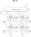
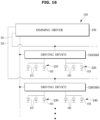
- FIG. 10 is a circuit block diagram of a dimming driver and a light apparatus included in a display apparatusnt.
- FIG. 11 is a circuit block diagram of a driving device included in a display apparatus.
- the display apparatus 10 includes the dimming driver 170, a plurality of driving devices 310, 320, 330, and 340, collectively 300, and the plurality of light sources 111.
- the plurality of light sources may each include an LED, and may be classified into a plurality of dimming blocks 200.
- a plurality of light sources belonging to the same dimming block may form a group.
- a plurality of light sources belonging to a dimming block may receive the driving current with the same magnitude. Furthermore, a plurality of light sources belonging to a dimming block may emit light with the same intensity.
- the driving devices 300 may receive the analog dimming signal from the dimming driver 170 and store the received analog dimming signal while being input-activated by the dimming driver 170. Furthermore, while being input-activated, the plurality of driving devices 300 may apply a driving current corresponding to the stored analog dimming signal to the plurality of light sources.
- the plurality of dimming blocks 200 may be arranged in a plurality of rows and a plurality of columns. Driving devices that apply the driving current to light sources of dimming blocks belonging to the same row may share the same scan line.
- the first driving device 310 and the second driving device 320 may share the first scan line S1
- the third driving device 330 and the fourth driving device 340 may share the second scan line S2.
- driving devices that apply the driving current to light sources of dimming blocks belonging to the same column may share the same data line.
- the first driving device 310 and the third driving device 330 may share the first data line D1
- the second driving device 320 and the fourth driving device 340 may share the second data line D2.
- the plurality of driving devices 300 may be input-activated by scan signals of the dimming driver 170, and may receive the analog dimming signal from the dimming driver 170.
- the plurality of driving devices 300 may store the received analog dimming signal, and may apply a driving current to the plurality of light sources according to the stored analog dimming signal.
- the third driving device 330 and the fourth driving device 340 may apply driving currents to the plurality of light sources included in the third and fourth dimming blocks 230 and 240.
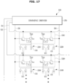
- each of the plurality of driving devices 300 may include a one-capacitor two-transistor (1C2T) topology circuit.
- Each of the plurality of driving devices 300 may include a driving transistor Tdr, a switching transistor Tsw, and a storage capacitor Cs.
- the driving transistor Tdr includes an input terminal, an output terminal, and a control terminal.
- the input terminal of the driving transistor Tdr may be connected to a power source Vdd, and the output terminal may be connected to a plurality of light sources.
- the driving transistor Tdr may apply a driving current to the plurality of light sources based on a voltage at the control terminal.
- the storage capacitor Cs is provided between the output terminal and the control terminal of the driving transistor Tdr.
- the storage capacitor Cs may output a constant voltage by storing input charges.
- the driving transistor Tdr may apply a driving current to the plurality of light sources based on a voltage output by the storage capacitor Cs.
- the switching transistor Tsw may be turned on by a scan signal of the scan line S1 or S2, and may deliver an analog dimming signal of the data line D1 or D2 to the storage capacitor Cs and the driving transistor Tdr.
- the analog dimming signal of the data line D1 or D2 is input to the control terminal of the driving transistor Tdr, and the driving transistor Tdr may apply a driving current corresponding to the analog dimming signal to the plurality of light sources.
- the storage capacitor Cs may store charges from the analog dimming signal, and output a voltage corresponding to the analog dimming signal.
- the storage capacitor Cs may still output the voltage corresponding to the analog dimming signal, and the driving transistor Tdr may still apply the driving current corresponding to the analog dimming signal to the plurality of light sources.
- a circuit as shown in FIG. 11 is an example of the driving device 300, without being limited thereto.
- the driving device 300 may include a 3T1C topology circuit obtained by adding a transistor to compensate for body effect of the driving transistor Tdr.
- the driving device 300 may be provided, for example, in a single chip in which the circuit shown in FIG. 11 is integrated. In other words, the circuit shown in FIG. 11 may be integrated in a single semiconductor chip.
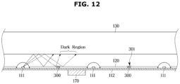
- FIG. 12 is a cross-sectional view of a dimming driver, driving devices and light sources included in a display apparatus.
- the driving devices 300 may be irregularly arranged in the dimming areas. Relative positions of the driving devices in the different dimming blocks may be different from one another.
- the front surface (a surface from which light is emitted) of the light source module 110 is partitioned into a first dimming area 410 corresponding to the first dimming block 210, a second dimming area 420 corresponding to the second dimming block 220, a third dimming area 430 corresponding to the third dimming block 230, and a fourth dimming area 440 corresponding to the fourth dimming block 240.
- the first driving device 310 is arranged in a lower right portion from the center of the first dimming area 410, and the second driving device 320 is arranged in an upper left portion from the center of the second dimming area 420. Furthermore, the third driving device 330 is arranged in an upper right portion from the center of the third dimming area 430, and the fourth driving device 340 is arranged in a lower left portion from the center of the fourth dimming area 440.
- Arrangement of the first driving device 310 in the first dimming area 410 is different from arrangement of the second and third driving devices 320 and 330 in the second and third dimming areas 420 and 430 adjacent to the first dimming area 410. Furthermore, arrangement of the second driving device 320 in the second dimming area 420 is different from arrangement of driving devices in the adjacent dimming areas to the second dimming area 420.
- arrangement of a driving device in a dimming area is different from arrangement of driving devices in other dimming areas adjacent to the former dimming area.
- different arrangement represents that a relative location of a driving device from the center of a dimming area is different.
- the first dimming area 410, the second dimming area 420, the third dimming area 430, and the fourth dimming area 440 are arranged in a plurality of rows and a plurality of columns.
- arrangement of a driving device in one of a plurality of dimming areas arranged in a plurality of rows and a plurality of columns is different from arrangement of a driving device in another dimming area belonging to the same row or column as the one dimming area and adjacent to the one dimming area.
- a driving device in one of a plurality of dimming areas arranged in a plurality of rows and a plurality of columns is arranged out of (i.e., outside) a virtual line defined by two driving devices in two dimming areas belonging to the same row as the one dimming area and adjacent to the one dimming area.
- the first driving device 310 in the first dimming area 410 in the first row and first column is arranged on the right from the center of the dimming area
- the second driving device 320 in the second dimming area 420 in the first row and second column is arranged on the left from the center of the dimming area.
- driving devices in a plurality dimming areas arranged in the same row are arranged alternately on the left and right from the center of the dimming area.
- the first driving device 310 in the first dimming area 410 in the first row and first column is arranged in a lower portion from the center of the dimming area
- the third driving device 330 in the third dimming area 430 in the second row and first column is arranged in an upper portion from the center of the dimming area.
- driving devices in a plurality dimming areas arranged in the same column are arranged alternately above and below the center of the dimming area.
- the first driving device 310 is arranged closest to the second driving device 320 and the third driving device 330, and the first to third driving devices 310, 320, and 330 are not arranged in a straight line. In other words, the first driving device 310 is arranged out of (i.e., outside) a virtual line that connects the second driving device 320 and the third driving device 330 closest to the first driving device 310.
- one of the plurality of driving devices is arranged out of a virtual line defined by two driving devices closest to the one driving device.
- the plurality of driving devices may be arranged irregularly or in arbitrary positions in the plurality of dimming areas.
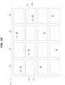
- FIG. 14 is a plan view of an example arrangement of driving devices included in a display apparatus.
- driving devices of four neighboring dimming areas in the same row may be arranged in different positions with respect to the center of the dimming areas.
- the plurality of driving devices 500 may receive an analog dimming signal from the dimming driver 170, and may apply a driving current to the plurality of light sources 111 according to the received analog dimming signal.
- dimming areas where driving devices are located and dimming areas where no driving device is located are alternately arranged. Furthermore, in the same column, dimming areas where driving devices are located and dimming areas where no driving device is located are alternately arranged.
- arrangement of a driving device in a dimming area may be different from arrangement of the other driving device adjacent to the one driving device in another dimming area.
- FIG. 19 is a plan view of driving devices included in a display apparatus, according to an embodiment.
- arrangement of a driving device in a dimming area may be different from arrangement of the other driving device adjacent to the one driving device in another dimming area.
- FIG. 20 is a plan view of driving devices included in a display apparatus, according to an embodiment.
- the first driving device 510 may be located in a lower portion of the first dimming area 410
- the second driving device 520 may be located in an upper portion of the fourth dimming area 440
- the third driving device 530 may be located in an upper portion of the fifth dimming area 450
- the fourth driving device 540 may be located in a lower portion of the eighth dimming area 480.
- dimming areas where driving devices are located and dimming areas where no driving device is located are alternately arranged.
- arrangement of a driving device in a dimming area may be different from arrangement of the other driving device adjacent to the one driving device in another dimming area.
- FIG. 21 is a plan view of driving devices included in a display apparatus, according to an embodiment.
- Each of the driving devices 600 may apply a driving current to light sources included in four dimming blocks.
- a driving area 700 For example, an area defined by light sources included in four dimming blocks driven by a single driving device may be defined as a driving area 700.
- the first driving device 610 disposed at a first position in a first driving area 710, may apply a driving current to light sources arranged in the first driving area 710 including four dimming blocks
- the second driving device 620 disposed at a second position in a second driving area 720, may apply a driving current to light sources arranged in the second driving area 720 including four dimming blocks.
- the first driving area is adjacent to the second driving area.
- Arrangement of driving devices 600 is different depending on the driving area 700.
- a location of a driving device in a driving area is different from a location of a driving device in another driving area adjacent to the former driving area.
- the first and second position are located in relatively different areas of the first driving area 710 and the second driving area 720, respectively. That is, consistent with the above discussion at e.g. Figs. 13 , 14 , 15 , 18 , 19 , & 20 , the first driving device 610 and second driving device 620 are irregularly arranged with respect to the front surface (from which light is emitted) of the display apparatus.
- an arrangement of a driving device in one dimming area of the plurality of dimming areas is different from arrangements of driving devices in other dimming areas adjacent to the one dimming area.
- the plurality of dimming areas may be arranged in a plurality of rows and a plurality of columns, and an arrangement of a driving device in one dimming area of the plurality of dimming areas may be different from arrangements of driving devices in other dimming areas arranged in the same row or column as the one dimming area and adjacent to the one dimming area.
- one driving device of the plurality of driving devices may be arranged out of (i.e., outside) a virtual line defined by two driving devices closest to the one driving device.
- an optical defect due to the plurality of driving devices may be prevented or suppressed.
- the plurality of dimming blocks may emit light with at least different brightnesses. In other words, local dimming is implemented.
- Each of the plurality of driving devices may apply a driving current to light sources included in at least two dimming blocks.
- the number of the plurality of driving devices may be reduced, and furthermore, an optical defect due to the plurality of driving devices may be reduced as well.
- One driving device of the plurality of driving devices may be arranged in a dimming area defined by one dimming block of the at least two dimming blocks.
- a dimming area where the driving device is arranged and a dimming area where the one driving device is not arranged may be alternately arranged.
- an arrangement of a driving device in a driving area defined by the at least two dimming blocks may be different from arrangements of driving devices in other driving areas adjacent to the driving area.
- an optical defect due to the plurality of driving devices may be prevented or suppressed.
- a dimming driver may be further included on a second surface of the substrate to provide a dimming signal to the plurality of driving devices.
- the dimming driver may provide the dimming signal to the plurality of driving devices in an active matrix scheme.
- the plurality of driving devices may be arranged in a plurality of rows and a plurality of columns, and the dimming driver may provide a scan signal to driving devices arranged in one of the plurality of rows and provide the dimming signal to driving devices arranged in the plurality of columns.
- the number of pins for the dimming driver to provide a dimming signal to a plurality of driving devices is reduced.
- the at least one light source may include an LED directly contacting wiring on the substrate and an optical dome covering the LED.
- the LED has a DBR formed on a surface from which light is emitted
- the LED may emit more intense light in a lateral direction than in the perpendicular direction.
Landscapes
- Physics & Mathematics (AREA)
- Engineering & Computer Science (AREA)
- General Physics & Mathematics (AREA)
- Theoretical Computer Science (AREA)
- Computer Hardware Design (AREA)
- Crystallography & Structural Chemistry (AREA)
- Nonlinear Science (AREA)
- Chemical & Material Sciences (AREA)
- Optics & Photonics (AREA)
- Mathematical Physics (AREA)
- Control Of Indicators Other Than Cathode Ray Tubes (AREA)
- Liquid Crystal (AREA)
- Planar Illumination Modules (AREA)
Claims (15)
- Dispositif d'affichage (10), comprenant :un panneau à cristaux liquides ;une pluralité de sources d'éclairage (111) configurées pour émettre un éclairage ;un substrat comprenant une pluralité de zones d'attaque (700) sur un premier côté du substrat, chaque zone d'attaque (710 à 740) de la pluralité de zones d'attaque (700) comprenant une pluralité de blocs de gradation (200), et chaque bloc de gradation de la pluralité de blocs de gradation (200) comprenant au moins une source d'éclairage de la pluralité de sources d'éclairage (111) ; etune pluralité de dispositifs d'attaque (300 ; 500 ; 600) sur le premier côté du substrat, chaque dispositif d'attaque de la pluralité de dispositifs d'attaque (300 ; 500 ; 600) étant prévu dans une zone d'attaque respective (710 à 740) de la pluralité de zones d'attaque (700) et étant configuré pour commander un courant d'attaque de l'au moins une source d'éclairage dans chaque bloc de gradation dans la zone d'attaque respective (710 à 740), dans lequel un premier dispositif d'attaque (610) de la pluralité de dispositifs d'attaque (600) est disposé à une première position dans une première zone d'attaque (710) de la pluralité de zones d'attaque (700),dans lequel un deuxième dispositif d'attaque (620) de la pluralité de dispositifs d'attaque (600) est disposé à une deuxième position dans une deuxième zone d'attaque (720) de la pluralité de zones d'attaque (700),dans lequel un troisième dispositif d'attaque (630) de la pluralité de dispositifs d'attaque (600) est disposé à une troisième position dans une troisième zone d'attaque (730) de la pluralité de zones d'attaque,dans lequel la deuxième zone d'attaque (720) est adjacente à la première zone d'attaque (710) dans la direction des rangées, etla troisième zone d'attaque (730) est adjacente à la première zone d'attaque (710) dans la direction des colonnes,dans lequella première position et la troisième position sont situées dans des zones relativement différentes de la première zone d'attaque (710) et de la troisième zone d'attaque (730), respectivement, et caractérisé en ce que :
la première position et la deuxième position sont situées dans des zones relativement différentes de la première zone d'attaque (710) et de la deuxième zone d'attaque (720), respectivement. - Dispositif d'affichage (10) selon la revendication 1, dans lequel chaque zone d'attaque (710 à 740) de la pluralité de zones d'attaque (700) est définie par l'au moins une source d'éclairage dans chaque bloc de gradation dans la zone d'attaque recevant un courant d'attaque en provenance d'un dispositif d'attaque respectif de la pluralité de dispositifs d'attaque.
- Dispositif d'affichage (10) selon la revendication 1, dans lequel chaque bloc de gradation de la pluralité de blocs de gradation (200) est défini par chaque source d'éclairage de l'au moins une source d'éclairage dans le bloc de gradation recevant un même courant d'attaque provenant d'un même dispositif d'attaque de la pluralité de dispositifs d'attaque (300 ; 500 ; 600).
- Dispositif d'affichage (10) selon la revendication 3, dans lequel la pluralité de dispositifs d'attaque (300 ; 500 ; 600) sont configurés pour fournir différents courants d'attaque à des sources d'éclairage dans différents blocs de gradation (200).
- Dispositif d'affichage selon la revendication 1, dans lequel chaque zone d'attaque (710 à 740) de la pluralité de zones d'attaque (700) comprend quatre blocs de gradation (200).
- Dispositif d'affichage (10) selon la revendication 1, dans lequel la première position est située sur une demi-zone supérieure de la première zone d'attaque (710), et la deuxième position est située sur une demi-zone inférieure de la deuxième zone d'attaque (720).
- Dispositif d'affichage (10) selon la revendication 1, dans lequel la première position est située sur une demi-zone gauche de la première zone d'attaque (710) et la troisième position est située sur une demi-zone droite de la troisième zone d'attaque (730).
- Dispositif d'affichage (10) selon la revendication 1, dans lequel la pluralité de dispositifs d'attaque et la pluralité de sources d'éclairage sont prévues sur le premier côté du substrat.
- Dispositif d'affichage (10) selon la revendication 8, dans lequel chaque dispositif d'attaque de la pluralité de dispositifs d'attaque est configuré pour recevoir un signal à travers un second côté du substrat.
- Dispositif d'affichage (10) selon la revendication 1, dans lequel un quatrième dispositif d'attaque (640) de la pluralité de dispositifs d'attaque (600) est disposé à une quatrième position dans une quatrième zone d'attaque (740) de la pluralité de zones d'attaque qui est adjacente à la deuxième zone d'attaque (720) et à la troisième zone d'attaque (730), et
la première position et la quatrième position sont situées dans des zones relativement différentes de la première zone d'attaque (710) et de la quatrième zone d'attaque (740), respectivement. - Dispositif d'affichage (10) selon la revendication 1, dans lequel chaque dispositif d'attaque de la pluralité de dispositifs d'attaque comprend (300 ; 500 ; 600) :un premier transistor (Tdr1) ;un condensateur (Cs1) couplé à une borne de commande du premier transistor (Tdr1) ; etun deuxième transistor (Tsw1) couplé à la borne de commande du premier transistor (Tdr1).
- Dispositif d'affichage (10) selon la revendication 1, dans lequel la pluralité de dispositifs d'attaque comprend (300 ; 500 ; 600) sont commandés par un procédé de matrice active.
- Dispositif d'affichage (10) selon la revendication 10,dans lequella première zone d'attaque (710) et la deuxième zone d'attaque (720) sont disposées sur une première rangée, la troisième zone d'attaque (730) et la quatrième zone d'attaque (740) sont disposées sur une deuxième rangée, la première zone d'attaque (710) et la troisième zone d'attaque (730) sont disposées sur une première colonne, la deuxième zone d'attaque (720) et la quatrième zone d'attaque (740) sont disposées sur une deuxième colonne, la deuxième position et la quatrième position sont situées dans des zones relativement différentes de la deuxième zone d'attaque (720) et de la quatrième zone d'attaque (740), respectivement, etla troisième position et la quatrième position sont situées dans des zones relativement différentes de la troisième zone d'attaque (730) et de la quatrième zone d'attaque (740), respectivement.
- Dispositif d'affichage (10) selon la revendication 13, comprenant en outre :une première ligne de balayage (S1) couplée au premier dispositif d'attaque (310) et au deuxième dispositif d'attaque (320) ;une deuxième ligne de balayage (S2) couplée au troisième dispositif d'attaque (330) et au quatrième dispositif d'attaque (340) ;une première ligne de données (D1) couplée au premier dispositif d'attaque (310) et au troisième dispositif d'attaque (330), etune deuxième ligne de données (D2) couplée au deuxième dispositif d'attaque (320) et au quatrième dispositif d'attaque (340).
- Dispositif d'affichage (10) selon la revendication 14, comprenant en outre un pilote de gradation (170) configuré pour :dans une première durée, activer le premier dispositif d'attaque (310) et le deuxième dispositif d'attaque (320) via la première ligne de balayage (S1) et fournir un signal de gradation au premier dispositif d'attaque (310) et au deuxième dispositif d'attaque (320) via la première ligne de données (D1) et la deuxième ligne de données (D2), respectivement, etdans une deuxième durée, activer le troisième dispositif d'attaque (330) et le quatrième dispositif d'attaque (340) via la deuxième ligne de balayage (S2) et fournir un signal de gradation à chacun du troisième dispositif d'attaque (330) et du quatrième dispositif d'attaque (340) via la première ligne de données (D1) et la deuxième ligne de données (D2), respectivement.
Priority Applications (5)
| Application Number | Priority Date | Filing Date | Title |
|---|---|---|---|
| EP25172850.7A EP4567781A3 (fr) | 2020-12-03 | 2021-09-03 | Appareil d'affichage et son dispositif d'éclairage |
| DE202021105372.0U DE202021105372U1 (de) | 2020-12-03 | 2021-10-05 | Anzeigeeinrichtung und Beleuchtungseinrichtung davon |
| DE202021105374.7U DE202021105374U1 (de) | 2020-12-03 | 2021-10-05 | Anzeigeeinrichtung und Beleuchtungseinrichtung davon |
| DE202021105375.5U DE202021105375U1 (de) | 2020-12-03 | 2021-10-05 | Anzeigeeinrichtung und Beleuchtungseinrichtung davon |
| DE202021106629.6U DE202021106629U1 (de) | 2020-12-03 | 2021-12-03 | Anzeigeeinrichtung und Beleuchtungseinrichtung davon |
Applications Claiming Priority (2)
| Application Number | Priority Date | Filing Date | Title |
|---|---|---|---|
| KR20200167251 | 2020-12-03 | ||
| KR1020200182552A KR102361974B1 (ko) | 2020-12-03 | 2020-12-23 | 디스플레이 장치 및 그 광원 장치 |
Related Child Applications (2)
| Application Number | Title | Priority Date | Filing Date |
|---|---|---|---|
| EP25172850.7A Division EP4567781A3 (fr) | 2020-12-03 | 2021-09-03 | Appareil d'affichage et son dispositif d'éclairage |
| EP25172850.7A Division-Into EP4567781A3 (fr) | 2020-12-03 | 2021-09-03 | Appareil d'affichage et son dispositif d'éclairage |
Publications (3)
| Publication Number | Publication Date |
|---|---|
| EP4009315A1 EP4009315A1 (fr) | 2022-06-08 |
| EP4009315B1 true EP4009315B1 (fr) | 2025-06-25 |
| EP4009315C0 EP4009315C0 (fr) | 2025-06-25 |
Family
ID=77640412
Family Applications (1)
| Application Number | Title | Priority Date | Filing Date |
|---|---|---|---|
| EP21194729.6A Active EP4009315B1 (fr) | 2020-12-03 | 2021-09-03 | Appareil d'affichage et son dispositif d'éclairage |
Country Status (4)
| Country | Link |
|---|---|
| EP (1) | EP4009315B1 (fr) |
| KR (1) | KR102454913B1 (fr) |
| DE (1) | DE202021105026U1 (fr) |
| WO (1) | WO2022059870A1 (fr) |
Families Citing this family (11)
| Publication number | Priority date | Publication date | Assignee | Title |
|---|---|---|---|---|
| EP4394492A4 (fr) * | 2022-03-29 | 2025-04-16 | Samsung Electronics Co., Ltd. | Dispositif d'affichage et dispositif de source de lumière associé |
| WO2023191268A1 (fr) * | 2022-03-29 | 2023-10-05 | 삼성전자주식회사 | Dispositif d'affichage et dispositif de source de lumière associé |
| KR102713352B1 (ko) * | 2022-07-26 | 2024-10-07 | 삼성전자주식회사 | 디스플레이 장치 및 그 광원 장치 |
| WO2024025083A1 (fr) * | 2022-07-26 | 2024-02-01 | 삼성전자주식회사 | Appareil d'affichage et dispositif de source de lumière associé |
| EP4465124A4 (fr) | 2022-07-26 | 2025-06-11 | Samsung Electronics Co., Ltd. | Appareil d'affichage et dispositif de source de lumière associé |
| CN120153310A (zh) | 2023-02-16 | 2025-06-13 | 三星电子株式会社 | 显示装置及其光源装置 |
| KR20240127795A (ko) * | 2023-02-16 | 2024-08-23 | 삼성전자주식회사 | 디스플레이 장치 및 그 광원 장치 |
| US12242157B2 (en) | 2023-03-16 | 2025-03-04 | Samsung Electronics Co., Ltd. | Light source apparatus, method for manufacturing light source apparatus, and display apparatus comprising light source apparatus |
| WO2024191005A1 (fr) * | 2023-03-16 | 2024-09-19 | 삼성전자주식회사 | Appareil de source de lumière, procédé de fabrication d'appareil de source de lumière et appareil d'affichage comprenant un appareil de source de lumière |
| KR20250104973A (ko) * | 2023-12-29 | 2025-07-08 | 삼성전자주식회사 | 디스플레이 장치 |
| KR20250114868A (ko) * | 2024-01-22 | 2025-07-29 | 삼성전자주식회사 | 디스플레이 장치 및 그 광원 장치 |
Family Cites Families (9)
| Publication number | Priority date | Publication date | Assignee | Title |
|---|---|---|---|---|
| KR101493492B1 (ko) * | 2007-09-14 | 2015-03-06 | 삼성디스플레이 주식회사 | 백라이트 유닛, 이를 포함하는 액정 표시 장치 및 이의구동방법 |
| KR101621550B1 (ko) * | 2009-08-28 | 2016-05-17 | 엘지전자 주식회사 | 광학 어셈블리, 그를 구비한 백라이트 유닛 및 디스플레이 장치 |
| KR101423518B1 (ko) * | 2009-09-30 | 2014-08-01 | 엘지디스플레이 주식회사 | 액정표시장치 |
| RU2586385C2 (ru) * | 2011-09-20 | 2016-06-10 | Конинклейке Филипс Н.В. | Светоизлучающий модуль, лампа, осветительное устройство и устройство отображения |
| EP3564742B1 (fr) * | 2012-10-30 | 2022-02-23 | Sharp Kabushiki Kaisha | Substrat de matrice active et panneau d'affichage le comprenant |
| KR102330105B1 (ko) * | 2015-03-24 | 2021-11-25 | 삼성전자주식회사 | 디스플레이장치 |
| KR102618734B1 (ko) * | 2018-11-19 | 2023-12-29 | 삼성디스플레이 주식회사 | 표시 장치 및 이의 구동 방법 |
| KR102577240B1 (ko) * | 2018-11-21 | 2023-09-12 | 삼성디스플레이 주식회사 | 타일드 표시 장치 |
| KR102512914B1 (ko) * | 2018-12-28 | 2023-03-22 | 엘지디스플레이 주식회사 | 디스플레이 패널, 디스플레이 장치 및 구동회로 |
-
2021
- 2021-03-08 WO PCT/KR2021/002832 patent/WO2022059870A1/fr not_active Ceased
- 2021-09-03 DE DE202021105026.8U patent/DE202021105026U1/de active Active
- 2021-09-03 EP EP21194729.6A patent/EP4009315B1/fr active Active
- 2021-12-28 KR KR1020210189509A patent/KR102454913B1/ko active Active
Also Published As
| Publication number | Publication date |
|---|---|
| EP4009315A1 (fr) | 2022-06-08 |
| EP4009315C0 (fr) | 2025-06-25 |
| KR20220078522A (ko) | 2022-06-10 |
| DE202021105026U1 (de) | 2021-10-18 |
| WO2022059870A1 (fr) | 2022-03-24 |
| KR102454913B1 (ko) | 2022-10-17 |
Similar Documents
| Publication | Publication Date | Title |
|---|---|---|
| EP4009315B1 (fr) | Appareil d'affichage et son dispositif d'éclairage | |
| US12283255B2 (en) | Display apparatus and light apparatus thereof | |
| KR102758863B1 (ko) | 디스플레이 장치 및 그 광원 장치 | |
| US20240393642A1 (en) | Display apparatus and backlight unit | |
| KR20230026128A (ko) | 디스플레이 장치 및 백라이트 유닛 | |
| US12505812B2 (en) | Display apparatus | |
| KR20230166776A (ko) | 디스플레이 장치 및 그 광원 장치 | |
| EP4567781A2 (fr) | Appareil d'affichage et son dispositif d'éclairage | |
| CN114648963B (zh) | 显示设备及发光装置 | |
| KR102660579B1 (ko) | 디스플레이 장치 및 그 광원 장치 | |
| US12085802B2 (en) | Display apparatus and light source apparatus thereof | |
| US11934064B2 (en) | Display apparatus and light source apparatus thereof | |
| KR20230168913A (ko) | 디스플레이 장치 | |
| CN118215879A (zh) | 显示装置及其光源装置 | |
| CN120153310A (zh) | 显示装置及其光源装置 | |
| KR20230018224A (ko) | 디스플레이 장치 |
Legal Events
| Date | Code | Title | Description |
|---|---|---|---|
| PUAI | Public reference made under article 153(3) epc to a published international application that has entered the european phase |
Free format text: ORIGINAL CODE: 0009012 |
|
| STAA | Information on the status of an ep patent application or granted ep patent |
Free format text: STATUS: EXAMINATION IS IN PROGRESS |
|
| 17P | Request for examination filed |
Effective date: 20210903 |
|
| AK | Designated contracting states |
Kind code of ref document: A1 Designated state(s): AL AT BE BG CH CY CZ DE DK EE ES FI FR GB GR HR HU IE IS IT LI LT LU LV MC MK MT NL NO PL PT RO RS SE SI SK SM TR |
|
| RBV | Designated contracting states (corrected) |
Designated state(s): AL AT BE BG CH CY CZ DE DK EE ES FI FR GB GR HR HU IE IS IT LI LT LU LV MC MK MT NL NO PL PT RO RS SE SI SK SM TR |
|
| GRAP | Despatch of communication of intention to grant a patent |
Free format text: ORIGINAL CODE: EPIDOSNIGR1 |
|
| STAA | Information on the status of an ep patent application or granted ep patent |
Free format text: STATUS: GRANT OF PATENT IS INTENDED |
|
| INTG | Intention to grant announced |
Effective date: 20250414 |
|
| GRAS | Grant fee paid |
Free format text: ORIGINAL CODE: EPIDOSNIGR3 |
|
| GRAA | (expected) grant |
Free format text: ORIGINAL CODE: 0009210 |
|
| STAA | Information on the status of an ep patent application or granted ep patent |
Free format text: STATUS: THE PATENT HAS BEEN GRANTED |
|
| AK | Designated contracting states |
Kind code of ref document: B1 Designated state(s): AL AT BE BG CH CY CZ DE DK EE ES FI FR GB GR HR HU IE IS IT LI LT LU LV MC MK MT NL NO PL PT RO RS SE SI SK SM TR |
|
| REG | Reference to a national code |
Ref country code: GB Ref legal event code: FG4D |
|
| REG | Reference to a national code |
Ref country code: CH Ref legal event code: EP |
|
| REG | Reference to a national code |
Ref country code: DE Ref legal event code: R096 Ref document number: 602021032727 Country of ref document: DE |
|
| REG | Reference to a national code |
Ref country code: CH Ref legal event code: EP |
|
| REG | Reference to a national code |
Ref country code: IE Ref legal event code: FG4D |
|
| U01 | Request for unitary effect filed |
Effective date: 20250716 |
|
| U07 | Unitary effect registered |
Designated state(s): AT BE BG DE DK EE FI FR IT LT LU LV MT NL PT RO SE SI Effective date: 20250723 |
|
| PG25 | Lapsed in a contracting state [announced via postgrant information from national office to epo] |
Ref country code: GR Free format text: LAPSE BECAUSE OF FAILURE TO SUBMIT A TRANSLATION OF THE DESCRIPTION OR TO PAY THE FEE WITHIN THE PRESCRIBED TIME-LIMIT Effective date: 20250926 Ref country code: NO Free format text: LAPSE BECAUSE OF FAILURE TO SUBMIT A TRANSLATION OF THE DESCRIPTION OR TO PAY THE FEE WITHIN THE PRESCRIBED TIME-LIMIT Effective date: 20250925 |
|
| PGFP | Annual fee paid to national office [announced via postgrant information from national office to epo] |
Ref country code: GB Payment date: 20250820 Year of fee payment: 5 |
|
| PG25 | Lapsed in a contracting state [announced via postgrant information from national office to epo] |
Ref country code: HR Free format text: LAPSE BECAUSE OF FAILURE TO SUBMIT A TRANSLATION OF THE DESCRIPTION OR TO PAY THE FEE WITHIN THE PRESCRIBED TIME-LIMIT Effective date: 20250625 |
|
| PG25 | Lapsed in a contracting state [announced via postgrant information from national office to epo] |
Ref country code: RS Free format text: LAPSE BECAUSE OF FAILURE TO SUBMIT A TRANSLATION OF THE DESCRIPTION OR TO PAY THE FEE WITHIN THE PRESCRIBED TIME-LIMIT Effective date: 20250925 |
|
| U20 | Renewal fee for the european patent with unitary effect paid |
Year of fee payment: 5 Effective date: 20250924 |
|
| PG25 | Lapsed in a contracting state [announced via postgrant information from national office to epo] |
Ref country code: IS Free format text: LAPSE BECAUSE OF FAILURE TO SUBMIT A TRANSLATION OF THE DESCRIPTION OR TO PAY THE FEE WITHIN THE PRESCRIBED TIME-LIMIT Effective date: 20251025 |
|
| PG25 | Lapsed in a contracting state [announced via postgrant information from national office to epo] |
Ref country code: SM Free format text: LAPSE BECAUSE OF FAILURE TO SUBMIT A TRANSLATION OF THE DESCRIPTION OR TO PAY THE FEE WITHIN THE PRESCRIBED TIME-LIMIT Effective date: 20250625 |
|
| PG25 | Lapsed in a contracting state [announced via postgrant information from national office to epo] |
Ref country code: CZ Free format text: LAPSE BECAUSE OF FAILURE TO SUBMIT A TRANSLATION OF THE DESCRIPTION OR TO PAY THE FEE WITHIN THE PRESCRIBED TIME-LIMIT Effective date: 20250625 |
|
| PG25 | Lapsed in a contracting state [announced via postgrant information from national office to epo] |
Ref country code: PL Free format text: LAPSE BECAUSE OF FAILURE TO SUBMIT A TRANSLATION OF THE DESCRIPTION OR TO PAY THE FEE WITHIN THE PRESCRIBED TIME-LIMIT Effective date: 20250625 |
|
| PG25 | Lapsed in a contracting state [announced via postgrant information from national office to epo] |
Ref country code: SK Free format text: LAPSE BECAUSE OF FAILURE TO SUBMIT A TRANSLATION OF THE DESCRIPTION OR TO PAY THE FEE WITHIN THE PRESCRIBED TIME-LIMIT Effective date: 20250625 |
|
| PG25 | Lapsed in a contracting state [announced via postgrant information from national office to epo] |
Ref country code: ES Free format text: LAPSE BECAUSE OF FAILURE TO SUBMIT A TRANSLATION OF THE DESCRIPTION OR TO PAY THE FEE WITHIN THE PRESCRIBED TIME-LIMIT Effective date: 20250625 |
|
| PLBE | No opposition filed within time limit |
Free format text: ORIGINAL CODE: 0009261 |
|
| STAA | Information on the status of an ep patent application or granted ep patent |
Free format text: STATUS: NO OPPOSITION FILED WITHIN TIME LIMIT |