EP4009326B1 - Datenpfadschnittstellenschaltung, speicher und speichersystem - Google Patents
Datenpfadschnittstellenschaltung, speicher und speichersystem Download PDFInfo
- Publication number
- EP4009326B1 EP4009326B1 EP21859353.1A EP21859353A EP4009326B1 EP 4009326 B1 EP4009326 B1 EP 4009326B1 EP 21859353 A EP21859353 A EP 21859353A EP 4009326 B1 EP4009326 B1 EP 4009326B1
- Authority
- EP
- European Patent Office
- Prior art keywords
- delay
- module
- data
- memory
- control
- Prior art date
- Legal status (The legal status is an assumption and is not a legal conclusion. Google has not performed a legal analysis and makes no representation as to the accuracy of the status listed.)
- Active
Links
Images


Classifications
-
- G—PHYSICS
- G11—INFORMATION STORAGE
- G11C—STATIC STORES
- G11C7/00—Arrangements for writing information into, or reading information out from, a digital store
- G11C7/22—Read-write [R-W] timing or clocking circuits; Read-write [R-W] control signal generators or management
-
- G—PHYSICS
- G06—COMPUTING OR CALCULATING; COUNTING
- G06F—ELECTRIC DIGITAL DATA PROCESSING
- G06F13/00—Interconnection of, or transfer of information or other signals between, memories, input/output devices or central processing units
- G06F13/14—Handling requests for interconnection or transfer
- G06F13/16—Handling requests for interconnection or transfer for access to memory bus
- G06F13/1668—Details of memory controller
- G06F13/1689—Synchronisation and timing concerns
-
- G—PHYSICS
- G11—INFORMATION STORAGE
- G11C—STATIC STORES
- G11C11/00—Digital stores characterised by the use of particular electric or magnetic storage elements; Storage elements therefor
- G11C11/21—Digital stores characterised by the use of particular electric or magnetic storage elements; Storage elements therefor using electric elements
- G11C11/34—Digital stores characterised by the use of particular electric or magnetic storage elements; Storage elements therefor using electric elements using semiconductor devices
- G11C11/40—Digital stores characterised by the use of particular electric or magnetic storage elements; Storage elements therefor using electric elements using semiconductor devices using transistors
- G11C11/401—Digital stores characterised by the use of particular electric or magnetic storage elements; Storage elements therefor using electric elements using semiconductor devices using transistors forming cells needing refreshing or charge regeneration, i.e. dynamic cells
- G11C11/4063—Auxiliary circuits, e.g. for addressing, decoding, driving, writing, sensing or timing
- G11C11/407—Auxiliary circuits, e.g. for addressing, decoding, driving, writing, sensing or timing for memory cells of the field-effect type
- G11C11/409—Read-write [R-W] circuits
- G11C11/4093—Input/output [I/O] data interface arrangements, e.g. data buffers
-
- G—PHYSICS
- G06—COMPUTING OR CALCULATING; COUNTING
- G06F—ELECTRIC DIGITAL DATA PROCESSING
- G06F3/00—Input arrangements for transferring data to be processed into a form capable of being handled by the computer; Output arrangements for transferring data from processing unit to output unit, e.g. interface arrangements
- G06F3/06—Digital input from, or digital output to, record carriers, e.g. RAID, emulated record carriers or networked record carriers
- G06F3/0601—Interfaces specially adapted for storage systems
- G06F3/0602—Interfaces specially adapted for storage systems specifically adapted to achieve a particular effect
- G06F3/061—Improving I/O performance
- G06F3/0611—Improving I/O performance in relation to response time
-
- G—PHYSICS
- G06—COMPUTING OR CALCULATING; COUNTING
- G06F—ELECTRIC DIGITAL DATA PROCESSING
- G06F3/00—Input arrangements for transferring data to be processed into a form capable of being handled by the computer; Output arrangements for transferring data from processing unit to output unit, e.g. interface arrangements
- G06F3/06—Digital input from, or digital output to, record carriers, e.g. RAID, emulated record carriers or networked record carriers
- G06F3/0601—Interfaces specially adapted for storage systems
- G06F3/0628—Interfaces specially adapted for storage systems making use of a particular technique
- G06F3/0638—Organizing or formatting or addressing of data
- G06F3/064—Management of blocks
-
- G—PHYSICS
- G11—INFORMATION STORAGE
- G11C—STATIC STORES
- G11C11/00—Digital stores characterised by the use of particular electric or magnetic storage elements; Storage elements therefor
- G11C11/21—Digital stores characterised by the use of particular electric or magnetic storage elements; Storage elements therefor using electric elements
- G11C11/34—Digital stores characterised by the use of particular electric or magnetic storage elements; Storage elements therefor using electric elements using semiconductor devices
- G11C11/40—Digital stores characterised by the use of particular electric or magnetic storage elements; Storage elements therefor using electric elements using semiconductor devices using transistors
- G11C11/401—Digital stores characterised by the use of particular electric or magnetic storage elements; Storage elements therefor using electric elements using semiconductor devices using transistors forming cells needing refreshing or charge regeneration, i.e. dynamic cells
- G11C11/4063—Auxiliary circuits, e.g. for addressing, decoding, driving, writing, sensing or timing
- G11C11/407—Auxiliary circuits, e.g. for addressing, decoding, driving, writing, sensing or timing for memory cells of the field-effect type
- G11C11/4076—Timing circuits
-
- G—PHYSICS
- G11—INFORMATION STORAGE
- G11C—STATIC STORES
- G11C16/00—Erasable programmable read-only memories
- G11C16/02—Erasable programmable read-only memories electrically programmable
- G11C16/06—Auxiliary circuits, e.g. for writing into memory
- G11C16/10—Programming or data input circuits
-
- G—PHYSICS
- G11—INFORMATION STORAGE
- G11C—STATIC STORES
- G11C29/00—Checking stores for correct operation ; Subsequent repair; Testing stores during standby or offline operation
- G11C29/02—Detection or location of defective auxiliary circuits, e.g. defective refresh counters
- G11C29/023—Detection or location of defective auxiliary circuits, e.g. defective refresh counters in clock generator or timing circuitry
-
- G—PHYSICS
- G11—INFORMATION STORAGE
- G11C—STATIC STORES
- G11C29/00—Checking stores for correct operation ; Subsequent repair; Testing stores during standby or offline operation
- G11C29/02—Detection or location of defective auxiliary circuits, e.g. defective refresh counters
- G11C29/028—Detection or location of defective auxiliary circuits, e.g. defective refresh counters with adaption or trimming of parameters
-
- G—PHYSICS
- G11—INFORMATION STORAGE
- G11C—STATIC STORES
- G11C7/00—Arrangements for writing information into, or reading information out from, a digital store
- G11C7/10—Input/output [I/O] data interface arrangements, e.g. I/O data control circuits, I/O data buffers
- G11C7/1051—Data output circuits, e.g. read-out amplifiers, data output buffers, data output registers, data output level conversion circuits
- G11C7/1066—Output synchronization
-
- G—PHYSICS
- G11—INFORMATION STORAGE
- G11C—STATIC STORES
- G11C7/00—Arrangements for writing information into, or reading information out from, a digital store
- G11C7/10—Input/output [I/O] data interface arrangements, e.g. I/O data control circuits, I/O data buffers
- G11C7/1078—Data input circuits, e.g. write amplifiers, data input buffers, data input registers, data input level conversion circuits
- G11C7/1093—Input synchronization
-
- G—PHYSICS
- G11—INFORMATION STORAGE
- G11C—STATIC STORES
- G11C2207/00—Indexing scheme relating to arrangements for writing information into, or reading information out from, a digital store
- G11C2207/22—Control and timing of internal memory operations
- G11C2207/2254—Calibration
-
- G—PHYSICS
- G11—INFORMATION STORAGE
- G11C—STATIC STORES
- G11C7/00—Arrangements for writing information into, or reading information out from, a digital store
- G11C7/10—Input/output [I/O] data interface arrangements, e.g. I/O data control circuits, I/O data buffers
- G11C7/1051—Data output circuits, e.g. read-out amplifiers, data output buffers, data output registers, data output level conversion circuits
- G11C7/1069—I/O lines read out arrangements
Definitions
- the present application relates to the field of integrated circuits, and more particularly, to a data path interface circuit, a memory and a memory system.
- a semiconductor memory is a memory that accesses through semiconductor circuits, and a Dynamic Random Access Memory (DRAM) is widely applied to various fields because of its high storage speed and high integration.
- DRAM Dynamic Random Access Memory
- Multiple memory blocks are generally arranged in the memory to achieve a greater memory space.
- data transmission speeds of the different memory blocks are different, which leads to timings of the different memory blocks are inconsistent, and transmission synchronization of stored data is not good.
- the present application provides a data path interface circuit, a memory and a memory system.
- the features of the data path interface circuit, the memory and the memory system according to the present application are defined in the independent claim, and the preferable features according to the present application are defined in the dependent claims.
- orientation or position relationships indicated by terms “upper”, “lower”, “vertical”, “horizontal”, “inner”, “outer”, and the like are orientation or position relationships shown in the drawings, are adopted not to indicate or imply that indicated devices or components must be in specific orientations or structured and operated in specific orientations but only to conveniently describe the embodiments of the present application and simplify descriptions and thus should not be understood as limits to the embodiments of the present application.
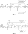
- FIG. 1 is a structural schematic diagram of a data path interface circuit 10 in a first embodiment.
- the data path interface circuit 10 includes a writing path module 100, a reading path module 200, a first delay module 300 and a delay control module 400.
- the data path interface circuit 10 is configured with an internal port 11 and an external port 12.
- the internal port 11 is configured to connect with a memory block 30 inside a memory, transmit stored data to be written to the memory block 30 or read the stored data from the memory block.
- the external port 12 is configured to receive the stored data to be written sent from an external electronic device or send the stored data read in the memory block 30 to the external electronic device.
- the writing path module 100 is connected to the internal port 11 and the external port 12 respectively, and is configured to transmit the stored data to the internal port 11 from the external port 12.
- An input end of the writing path module 100 is indirectly connected to the external port 12, specifically, the input end of the writing path module 100 is indirectly connected to the external port 12 through the first delay module 300, and an output end of the writing path module 100 is directly connected to the internal port 11. That is, the stored data to be written is input from the external electronic device, and reaches the memory block 30 through the external port 12, the first delay module 300, the writing path module 100 and the internal port 11 of the data path interface circuit, so that writing of the stored data is realized.
- the reading path module 200 is connected to the internal port 11 and the external port 12 respectively, and is configured to transmit the stored data to the external port 12 from the internal port 11.
- An input end of the reading path module 200 is indirectly connected to the internal port 11, specifically, the input end of the reading path module 200 is indirectly connected to the internal port 11 through the first delay module 300, and an output end of the reading path module 200 is directly connected to the external port 12. That is, the stored data is read from the memory block 30, and reaches the external electronic device through the internal port 11, the first delay module 300, the reading path module 200 and the external port 12 of the data path interface circuit, so that reading of the stored data is realized.
- the data path interface circuit 10 only executes one of writing operation and reading operation at the same time. As a result, the writing path module 100 and the reading path module 200 output the stored data in a time-sharing mode.
- the first delay module 300 is connected to the external port 12 and the internal port 11 respectively, and is configured to obtain the stored data from the external port 12 or the internal port 11, perform delay processing on the stored data, and transmit the delayed stored data to the writing path module 100 and/or the reading path module 200.
- the first delay module 300 obtains the stored data from the external port 11, performs delay processing on the stored data and transmits the delayed data to the writing path module 100.
- the stored data to be written are written from data pins of the memory.
- Each of the data pins is connected to multiple memory blocks 30, and is configured to transmit the stored data to the connected multiple memory blocks 30. It should be understood that length of transmission paths between the external port 12 of each data path interface circuit 10 and the data pins is not the same. As a result, even if the data reaches the data pins simultaneously, the stored data cannot reach each memory block 30 simultaneously based on similar data transmission speed and different lengths of the transmission paths.
- the first delay module 300 may perform delay processing on the received stored data for proper delay time, so that the stored data reaches the internal port 11 within a preset target time. In such a manner, the time that the stored data reaches the internal port 11 in each data path interface circuit 10 is the same or the time errors are within a bearable error range of the data path interface circuit 10, so that the unsynchronized transmission phenomenon of the stored data is solved.
- the first delay module 300 is configured with an output end.
- the output end is connected to a writing path module 100 and a reading path module 200 respectively.
- the first delay module 300 outputs the delayed stored data to the wiring path module 100 and the reading path module 200 simultaneously.
- one of the writing path module 100 and the reading path module 200 may be controlled to be enabled for outputting stored data.
- the first delay module 300 also may be configured with two output ends. The two output ends are respectively connected to a writing path module 100 and a reading path module 200 in a one-to-one correspondence. One of the two output ends of the first delay module 300 may be controlled to output stored data, so that only one of the writing path module 100 and the reading path module 200 may receive the stored data and output the stored data.
- a delay control module 400 is connected to the first delay module 300 and is configured to receive a signal instruction from external and control delay time for the first delay module 300 to perform the delay processing according to the signal instruction.
- the signal instruction is an instruction that is configured to indicate the data path interface circuit 10 to execute corresponding operation, for example, at least one of a write instruction, a read instruction or a mode selection coding instruction.
- the write instruction is configured to indicate the data path interface circuit 10 to execute corresponding writing operation.
- the delay control module 400 may be configured with one or more input ends, and may be configured to generate a control signal of the first delay module 300 according to a signal instruction from the input end. For example, if the delay control module 400 is configured with an input end, a control signal may be generated in response to one of the write instruction, the read instruction and the mode selection coding instruction. If the delay control module 400 is configured with two input ends, a control signal may be generated in response to two of the write instruction, the read instruction and the mode selection coding instruction. It should be understood that the more the types of signal instruction needed for the delay control module 400, the more complex the logistics of generating the control signal, and correspondingly the more reliable and comprehensive the control function. In such a manner, the reliability and the completeness of the data path interface circuit 10 may be improved, i.e., the transmission synchronization of the stored data is improved to a greater extent.
- the data path interface circuit 10 includes a writing path module 100, a reading path module 200, a first delay module 300 and a delay control module 400.
- the writing path module 100 is connected to an internal port 11 and an external port 12 respectively, and is configured to transmit stored data to the internal port 11 from the external port 12.
- the reading path module 200 is connected to the internal port 11 and the external port 12 respectively, and is configured to transmit the stored data to the external port 12 from the internal port 11.
- the first delay module 300 is connected to the external port 12 and the internal port 11 respectively, and is configured to obtain the stored data from the external port 12 or the internal port 11, perform delay processing on the stored data, and transmit the delayed stored data to the writing path module 100 and/or the reading path module 200.
- the delay control module 400 is connected to the first delay module 300 and is configured to receive a signal instruction from external and control delay time for the first delay module to perform the delay processing according to the signal instruction. Based on a control signal from the delay control module 400, the first delay module 300 may perform delay processing on the received stored data for proper delay time, so that the stored data reaches the internal port 11 or the external port 12 within a preset target time. In such a manner, the transmission time of the stored data in each data path interface circuit 10 between the internal port 11 and the external port 12 is the same, or transmission time errors are within a bearable error range of the data path interface circuit 10, so that the data path interface circuit 10 with better transmission synchronization on the stored data is realized.
- FIG. 2 is a schematic structural diagram of a data path interface circuit 10 in a second embodiment.
- the first delay module 300 includes a selection unit 310 and a temporary storage unit 320.
- a setting mode of the writing path module 100, the reading path module 200 and the delay control module 400 is the same with the setting mode in the embodiment in FIG. 1 , which is not detailed again herein.
- Input ends of the selection unit 310 are connected to the external port 12 and the internal port 11 respectively, and a control end of the selection unit 310 is configured to receive the signal instruction.
- the selection unit 310 is configured with two input ends, and the two input ends of the selection unit 310 are respectively connected to the internal port 11 and the external port 12 in a one-to-one correspondence to obtain stored data from the two ports respectively.
- the selection unit 310 is further configured with a control end, and the control end of the selection unit 310 is configured to receive a signal instruction to selectively output one of the received two stored data according to the signal instruction.
- the signal instruction may be a write instruction, so the selection unit 310 selectively outputs the stored data from the external port 12, so that writing of the data is realized.
- the selection unit 310 is a one-of-two multiplexer.
- the selection unit 310 also may be a one-of-three multiplexer and the like, that is, three input ends may be configured to realize a more complex selection function and transmission function.
- a data input end of the temporary storage unit 320 is connected to an output end of the selection unit 310, and a control end of the temporary storage unit 320 is connected to an output end of the delay control module 400.
- the temporary storage unit 320 includes at least one of a latch, a flip-flop or a register.
- a control end of the temporary storage unit 320 includes at least one of a clock drive end, a set end or a reset end.
- the temporary storage unit 320 may include a trigger, which is a D trigger.
- An input end of the D trigger is connected to the output end of the selection unit 310, the clock drive end of the D trigger is connected to the output end of the delay control module 400, and an output end of the D trigger is connected to the writing path module 100 and the reading path module 200 respectively.
- the D trigger samples a signal from the input end responsive to a control signal from the clock drive end.
- sampling time of the D trigger may be controlled, so that the stored data reaches the internal port 11 or the external port 12 within a target time through the writing path module 100 or the reading path module 200.
- a data path interface circuit 10 with better timing synchronization is realized.
- a preset enabling signal is output to the set end and/or the reset end, so that stable output of the temporary storage unit 320 may be ensured, and the reliability of the output signal of the data path interface circuit 10 is improved.
- the temporary storage unit 320 also may be other devices with signal temporary storage functions such as a JK trigger and a RS trigger.
- control signal includes at least one of a pulse signal, a signal rising edge or a signal falling edge. If the temporary storage unit 320 is a latch, it may be controlled through the pulse signal. If the temporary storage unit 320 is a flip-flop, it may be triggered through the signal rising edge or the signal falling edge. It should be understood that edge trigger may provide a greater timing margin, so as to improve the accuracy of sampling timing of the temporary storage unit 320, and then improve the reliability of the data path interface circuit 10.
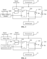
- FIG. 3 is a schematic structural diagram of a data path interface circuit 10 in a third embodiment.
- the writing path module 100 includes a writing buffer unit 100
- the reading path module 200 includes a reading buffer unit 210.
- a setting mode of the selection unit 310, the temporary storage unit 320 and the delay control module 400 is the same with the setting mode in the embodiment in FIG. 2 , which is not detailed again herein.
- An input end of the writing buffer unit 110 is connected to an output end of the temporary storage unit 320, an output end of the writing buffer unit 100 is connected to the internal port 11, and a control end of the writing buffer unit 110 is configured to receive the signal instruction.
- the writing buffer unit 110 buffers and outputs the delayed stored data from the input end responsive to the signal instruction received at the control end, so that further adjustment of timing is realized to provide a writing path module 100 with better timing accuracy during writing of the stored data and a data path interface circuit 10.
- An input end of the reading buffer unit 210 is connected to an output end of the temporary storage unit 320, an output end of the reading buffer unit 210 is connected to the external port 12, and a control end of the reading buffer unit 210 is configured to receive the signal instruction. Similar to the writing buffer unit 110, the reading buffer unit 210 may be set to provide a reading path module 200 with better timing accuracy during reading of the stored data and a data path interface circuit 10.
- FIG. 4 is a schematic structural diagram of a data path interface circuit 10 in a fourth embodiment.
- the delay control module 400 includes a delay chain 410 and a control signal generation circuit 420.
- a setting mode of the selection unit 310, the temporary storage unit 320, the writing buffer unit 110 and the reading buffer unit 210 is the same with the setting mode in the embodiment in FIG. 3 , which is not detailed again herein.
- An input end of the delay chain 410 is configured to receive the signal instruction, and the delay chain is configured to delay and output the signal instruction.
- the delay chain 410 may be a fixed delay chain 410.
- the fixed delay chain 410 may include multiple transmission grates connected in series. Each of the transmission gates is configured with a fixed delay time. Thus, a corresponding number of transmission gates may be set according to the preset delay time needed for the delay chain 410, so that a target preset delay time is generated.
- the fixed delay chain 410 may include an even number of inverters connected in series. By setting the even number of inverters, it may be ensured that an output delay signal corresponds to an electric level state of the input signal instruction, and there is only a difference in timing. Similar to the fixed delay chain 410 consisting of the aforementioned transmission gates, a corresponding number of inverters may be set according to the preset delay time needed for the delay chain 410, so that a target preset delay time is generated.
- the delay chain 410 may be a programmable delay chain 410. It should be understood that properties such as signal transmission speed in the data path interface circuit 10 may change with a temperature and other conditions of use environment. As a result, if conditions of the use environment change, there will be a risk of timing abnormality and even transmitted signal error.
- condition changes of the use environment of the data path interface circuit 10 may be detected by the detection structure, and the delay time of the programmable delay chain 410 may be adjusted according to the detected results, so that timing errors are avoided and a data path interface circuit with better reliability is provided.
- the detection structure may be a sensor which detects the use environment, so as to adjust the delay time according to changes of the environment.
- the detection structure also may be a feedback circuit, i.e., the input is fed back according to the timing of the signal output from the data path interface circuit 10, so that accuracy of the timing is improved through a closed-loop adjustment.
- the programmable delay chain 410 may include multiple delay units. Each of the delay units is configured to generate delay with a set step length, and realize adjustment on the delay time through a coding group.
- the coding group includes multiple control coding bits which are in one-to-one correspondence to the delay units.
- the programmable delay chain 410 includes 8 delay units, and the coding group includes 8 control coding bits. When a value of the coding group is 10000000, a first delay unit is controlled to turn on and other delay units are controlled to turn off, so that a delay with a set step length is generated.
- the programmable delay chain 410 may be controlled by changing the value of the coding group. It should be noted that the examples are only used for description, and not used to limit the programmable delay chain 410 and the coding group specifically.
- control signal generation circuit 420 is connected to an output end of the delay chain 410, and an output end of the control signal generation circuit 420 is connected to the control end of the temporary storage unit 320.
- the control signal generation circuit 420 is configured to generate a control signal according to a signal output from the delay chain 410.
- the control signal from the control signal generation circuit 420 is a pulse signal, a signal rising edge or a signal falling edge
- the control signal may realize a more reliable timing control function on the temporary storage unit 320.
- the signal instruction and the delayed signal instruction may not certainly in an expected control signal form.
- a control signal which may be matched with the timing of the delayed signal instruction and is in a target form may be generated through the control signal generation circuit 420, so that accurate control on the temporary storage unit 320 is realized.
- the first delay module 300 and the delay control module 400 are configured with two operating modes.
- the two operating modes include a delay mode and a quick mode.
- the delay mode the first delay module 300 and the delay control module 400 are valid.
- the quick mode the delay control module 400 is invalid, and transmission delay on the stored data by the first delay module 300 is zero.
- the first delay module 300 and the delay control module 400 are valid, which means that a delay function of the first delay module 300 is enabled, and the delay control module 400 may delay the stored data correspondingly by generating a control signal according to the signal instruction.
- the first delay module 300 and the delay control module 400 are invalid, which means that the first delay module 300 only enables a transmission function of the stored data, and does not enable the delay function, so that the stored data pass through quickly, thereby increasing the operating speed of the data path interface circuit 10.
- the aforementioned "transmission delay is zero" means that the first delay module 300 does not set extra delay time for the stored data, but the wires and other structures in the first delay module 300 have a certain inherent delay. The delay time of the inherent delay is very short, i.e., the inherent delay may be ignored.
- FIG. 5 is a structural schematic diagram of a data path interface circuit 10 in a fifth embodiment.
- the data path interface circuit 10 further includes a mode selection module 500.
- the mode selection module 500 is connected to the first delay module 300 and the delay control module 400 respectively, and is configured to receive the signal instruction, and control the operating modes of the first delay module 300 and the delay control module 400 according to the signal instruction. It should be understood that path lengths of receiving the stored data by the each of memory blocks 30 are different for different operating modes and different positions of the memory blocks 30. Thus, the data path interface circuit 10 corresponding to the memory block 30 with the longest data transmission path is set as the quick mode, so that the stored data passes through with highest speed.
- Data path interface circuits 10 of other memory blocks 30 are set as the delay mode, and the data path interface circuit 10 corresponding to each memory block 30 is controlled to generate corresponding delay, so that sum of transmission time consumed of the stored data on a transmission path and delay time are a set value, so that data transmission time corresponding each of the memory blocks 30 is the same.
- the set value may be transmission time corresponding the longest data transmission path.
- FIG. 6 is a structural schematic diagram of a memory in an embodiment.
- the memory includes a data path interface circuit 10, a data processing module 20 and a memory block 30.
- the data path interface circuit 10 is connected to the data processing module 20 and the memory block 30 respectively, so that timing processing on the transmitted stored data is realized.
- the data processing module 20 is connected to the external port of the data interface circuit 10, and is configured to process the stored data.
- the processing on the stored data by the data processing module 20 may be serial/parallel converting for stored data transmission. It should be understood that the data processing module 20 may also execute other types of processing on the stored data to achieve the purpose of improving the transmission speed of the stored data and the like.
- the memory block 30 is connected to the internal port 11 of the data interface circuit 10, and is configured to store the stored data.
- the memory block 30 may include at least two memory sub blocks 31, which are connected to a same memory block control circuit.
- the control circuit includes at least one of a row decoding circuit, a column decoding circuit or a redundant circuit.
- the control circuit may be shared to reduce the number of wirings in the memory, so that integral integration of the memory is improved. It should be understood that the control complexity also may be improved by sharing the control circuit. A proper circuit may be selected to share according to practical wiring needs, so that balance between integration and control difficulty is realized.
- FIG. 6 shows multiple bidirectional drivers 40, which are arranged on a transmission path of stored data.
- the bidirectional drivers 40 in FIG. 6 are only used to schematically illustrate the length of the transmission path and data transmission speed. Specifically, it means that the data transmission path provided with the bidirectional drivers 40 is relatively long, and the data transmission speed is relatively slow.
- the bidirectional drivers shown in FIG. 6 are not used to limit the specific structure of the data transmission path in the embodiments of the present application.
- the bidirectional drivers 40 on each transmission path are not limited to the number and the set positions shown in FIG. 6 .
- the memory includes the multiple data path interface circuits 10 and the multiple memory blocks 30, and the data path interface circuits 10 and the memory blocks 30 are set in one-to-one correspondence.
- the external ports 12 of the multiple data path interface circuits 10 are connected to the same data processing module 20.
- the internal ports 11 of the data path interface circuits 10 are connected to the multiple memory sub blocks 31.
- Read stored data may reach the data processing module 20 from the memory sub blocks 31 through the internal ports 11 and the external ports 12 of the interface circuits, so that reading of the data is realized.
- the written-in stored data may reach the memory sub blocks 31 from the data processing module 20 through the external ports 12 and the internal ports 11 of the interface circuits, so that written-in of the data is realized.
- transmission time matching includes that the data transmission time corresponding to each of the memory sub blocks 31 is completely the same, and errors among the data transmission time corresponding to different memory sub blocks 31 are within an acceptable range, i.e., accuracy of the stored data is not affected.
- two data processing modules 20 are configured to adapt to electronic devices with different configurations.
- the data processing modules 20 are connected to the multiple data path interface circuits 10 respectively.
- the data processing module 20 is controlled to enable for transmitting data.
- a set number of the data processing modules 20 are controlled to enable for synchronously transmitting data to the different memory blocks 30.
- the memory is applied to a computer with a 64-bit system, computation speed and addressing ability of the computer are relatively strong, and therefore, the two data processing modules 20 may be enabled simultaneously to realize higher data transmission speed.
- the memory When the memory is applied to a computer with a 32-bit system, only one data processing module 20 may be enabled, so that the stored data are ensured to be stably and reliably transmitted.
- the memory in the embodiment may select to enable a corresponding number of the data processing modules according to an external electronic device, so that application flexibility and universality of the memory are improved.
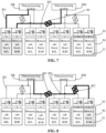
- FIG. 7 is a schematic diagram showing a operating mode in which two data processing modules are valid in an embodiment.
- the embodiment of FIG. 7 takes the access to a memory sub block B0L and a memory sub block B0H as an example.
- a data transmission path 202 is longer, so that the stored data needs to pass through a data path interface circuit 10 with a highest speed and reaches to the second data processing module 20H at a far end through a bidirectional driver 40 between circuits of the two data processing modules 20.
- a data transmission path 201 is shorter, so that the stored data are delayed for a time in the data path interface circuit 10, and are output to the corresponding drivers according to a direction of reading-writing operation.
- the delay time of the interface circuit is configured to match the bidirectional driver 40 in the middle and the length of the corresponding transmission path.
- data timings corresponding to the two memory sub blocks 31 may be kept consistent.
- An adjusting way for the delay time of other memory blocks 30 is the same with the adjusting way of the memory sub block B0L and the memory sub block B0H, which is not detailed again herein.
- FIG. 8 to FIG. 11 show a schematic diagram of a operating mode in which one data processing module 20 is valid of four embodiments.
- the access to a memory sub block B0L, a memory sub block B0H, a memory sub block B3L and a memory sub block B3H is taken as an example respectively to illuminate for a operating mode in which one data processing module 20 is valid.
- the longest transmission path is a data transmission path 203 (in black bold) from the first data processing module 20L to the memory sub block B3H.
- the data transmission path 203 is named as a timing datum path herein.
- the timing datum path includes wirings and the data path interface circuit 10.
- one bidirectional driver 40 and part of wirings are reduced on the data transmission path during access to the memory sub block B3L, and the transmission path is as shown in 204 in FIG. 9 (in black bold).
- a delay time circuit in the data path interface circuit 10 of the memory sub block B3L is operating, and the delay time is set to be matched with extra bidirectional driver 40 and related wirings on the data transmission path of the memory sub block B3H.
- delay time generated by the delay time circuit in the data path interface circuit 10 is limited if access to the memory sub block B0L and the memory sub block B0H is reading operation.
- a signal instruction for the memory sub block B0L and the memory sub block B0H needs to be delayed for the delay time, and then sends to the memory sub block B0L and the memory sub block B0H respectively.
- the delay time may be matched with delay time introduced through the middle bidirectional driver 40 on the data transmission path of the memory sub block B3L and the memory sub block B3H.
- a transmission path from the data processing module 20L to the memory sub block B0H is denoted by 205 in FIG. 10 (in black bold).
- a transmission path from the data processing module 20L to the memory sub block B0L is denoted by 201 in FIG. 11 (in black bold).
- FIG. 12 is a structural schematic diagram of a memory in another embodiment.
- FIG. 12 is a simplified drawing only showing a memory sub block B0L and a memory sub block B0H.
- the memory further includes a second delay module 50.
- the second delay module 50 may generate memory block control signal delay on the memory sub block B0L and the memory sub block B0H to further match with the delay time on the transmission path.
- the second delay module 50 is connected to a memory block 30, and is configured to receive the signal instruction and generate a control signal for the memory block 30 according to the signal instruction.
- the control signal of the memory block 30 is configured to control time when the stored data enters the memory block 30.
- the delay time generated on the memory block control signal by the second delay module 50 is matched with the delay time generated on the stored data by the data path interface circuit 10.
- the first delay module 300 and the second delay module 50 act simultaneously, so that transmission synchronization of the stored data among multiple memory sub blocks 31 may be further improved.
- delay time of the timing datum path 203 is recorded as T1
- delay time on wirings of the transmission path 204 is recorded as T2A
- delay time on the data path interface circuit 10 of the transmission path 204 is recorded as T2B
- delay time on wirings of the transmission path 205 is recorded as T3A
- delay time on the data path interface circuit 10 of the transmission path 205 is recorded as T3B
- delay time on wirings of the transmission path 201 in FIG.
- T4A delay time on the data path interface circuit 10 of the transmission path 201 (in FIG. 11 ) is recorded as T4B
- T4C delay time that the signal instruction passes through the second delay module 50 to generate the memory block control signal
- the embodiments of the present application further provide a memory system, which includes the memory such as above, an electronic device and a processing module controller.
- the processing module controller is connected to the memory and the electronic device respectively, and is configured to enable a corresponding number of the data processing modules in the memory according to system information of the electronic device.
- a memory system with higher stored data transmission synchronization is realized through the above structure.
- the specific setting mode of the memory may be referred to the above illustration, which is not detailed again herein
Landscapes
- Engineering & Computer Science (AREA)
- Theoretical Computer Science (AREA)
- Physics & Mathematics (AREA)
- General Engineering & Computer Science (AREA)
- General Physics & Mathematics (AREA)
- Computer Hardware Design (AREA)
- Microelectronics & Electronic Packaging (AREA)
- Human Computer Interaction (AREA)
- Memory System (AREA)
- Information Transfer Systems (AREA)
- Dram (AREA)
- Static Random-Access Memory (AREA)
- Communication Control (AREA)
Claims (14)
- Eine Datenpfad-Schnittstellenschaltung für einen Speicher, die Folgendes umfasst:ein Schreibpfadmodul (100), das mit einem internen Anschluss (11) bzw. einem externen Anschluss (12) des Speichers verbunden ist und so konfiguriert ist, dass es Daten vom externen Anschluss (12) an den internen Anschluss (11) überträgt;ein Lesepfadmodul (200), das mit dem internen Anschluss (11) bzw. dem externen Anschluss (12) verbunden und so konfiguriert ist, dass es die Daten vom internen Anschluss (11) an den externen Anschluss (12) überträgt;ein erstes Verzögerungsmodul (300), das mit dem externen Anschluss (12) bzw. dem internen Anschluss (11) verbunden ist und so konfiguriert ist, dass es die Daten von dem externen Anschluss (12) oder dem internen Anschluss (11) erhält, eine Verzögerungsverarbeitung an den Daten durchführt und verzögerte Daten an das Schreibpfadmodul (100) bzw. das Lesepfadmodul (200) überträgt; undein Verzögerungssteuermodul (400), das mit dem ersten Verzögerungsmodul (300) verbunden und so konfiguriert ist, dass es einen Signalbefehl empfängt, der von einer externen elektronischen Vorrichtung eingegeben wird, und ein Steuersignal an einem Ausgangsende entsprechend dem Signalbefehl erzeugt, wobei das Steuersignal so konfiguriert ist, dass es die Verzögerungszeit für das erste Verzögerungsmodul (300) steuert, um die Verzögerungsverarbeitung durchzuführen,dadurch gekennzeichnet, dass das erste Verzögerungsmodul (300) Folgendes umfasst:eine Auswahleinheit (310), wobei Eingangsenden der Auswahleinheit (310) mit dem externen Anschluss (12) bzw. dem internen Anschluss (11) verbunden sind, und ein Steuerende der Auswahleinheit so konfiguriert ist, dass es die Signalanweisung empfängt; undeine Zwischenspeichereinheit (320), wobei ein Dateneingangsende der Zwischenspeichereinheit (320) mit einem Ausgangsende der Auswahleinheit (310) verbunden ist, ein Ausgangsende der Zwischenspeichereinheit (320) mit dem Schreibpfadmodul (100) und dem Lesepfadmodul (200) verbunden ist und ein Steuerende der Zwischenspeichereinheit (320) mit dem Ausgangsende des Verzögerungssteuermoduls (400) verbunden ist, um das Steuersignal zu empfangen, und so konfiguriert ist, dass es als Reaktion auf das Steuersignal ein Signal an seinem Dateneingangsende speichert.
- Datenpfad-Schnittstellenschaltung nach Anspruch 1, wobei die Zwischenspeichereinheit (320) mindestens ein Latch, einen Flip-Flop oder ein Register umfasst; und ein Steuerende der Zwischenspeichereinheit (320) mindestens ein Takttreiberende, ein Setzende oder ein Rücksetzende umfasst.
- Die Datenpfad-Schnittstellenschaltung nach Anspruch 1, wobei das Schreibpfadmodul (100) umfasst:eine Schreibpuffereinheit (110), wobei ein Eingangsende der Schreibpuffereinheit (110) mit einem Ausgangsende der Zwischenspeichereinheit (320) verbunden ist, ein Ausgangsende der Schreibpuffereinheit (110) mit dem internen Port (11) verbunden ist und ein Steuerende der Schreibpuffereinheit (110) so konfiguriert ist, dass es den Signalbefehl empfängt; undwobei das Lesepfadmodul (200) Folgendes umfasst:
eine Lesepuffereinheit (210), wobei ein Eingangsende der Lesepuffereinheit (210) mit dem Ausgangsende der Zwischenspeichereinheit (320) verbunden ist, ein Ausgangsende der Lesepuffereinheit (210) mit dem externen Anschluss (12) verbunden ist und ein Steuerende der Lesepuffereinheit (210) so konfiguriert ist, dass es die Signalanweisung empfängt. - Die Datenpfad-Schnittstellenschaltung nach Anspruch 1, wobei das Verzögerungssteuermodul (400) umfasst:eine Verzögerungskette (410), wobei ein Eingangsende der Verzögerungskette (410) konfiguriert ist, um den Signalbefehl zu empfangen, wobei die Verzögerungskette (410) konfiguriert ist, um den Signalbefehl zu verzögern und auszugeben;undeine Steuersignal-Erzeugungsschaltung (420), wobei ein Eingangsende der Steuersignal-Erzeugungsschaltung (420) mit einem Ausgangsende der Verzögerungskette (410) verbunden ist, ein Ausgangsende der Steuersignal-Erzeugungsschaltung (420) mit dem Steuerende der Zwischenspeichereinheit (320) verbunden ist und die Steuersignal-Erzeugungsschaltung (420) so konfiguriert ist, dass sie ein Steuersignal entsprechend einem von der Verzögerungskette (410) ausgegebenen Signal erzeugt.
- Die Datenpfad-Schnittstellenschaltung nach Anspruch 4, wobei die Verzögerungskette (410) eine programmierbare Verzögerungskette ist.
- Datenpfad-Schnittstellenschaltung nach Anspruch 1, wobei das erste Verzögerungsmodul (300) und das Verzögerungssteuermodul (400) mit zwei Betriebsmodi konfiguriert sind, die einen Verzögerungsmodus und einen Schnellmodus umfassen; wobei in einem Fall des Verzögerungsmodus das erste Verzögerungsmodul (300)(300) und das Verzögerungssteuermodul (400) gültig sind; in einem Fall des Schnellmodus das Verzögerungssteuermodul (400) ungültig ist und die Übertragungsverzögerung der Daten durch das erste Verzögerungsmodul (300) Null ist; und wobei die Datenpfad-Schnittstellenschaltung ferner umfasst:
ein Modusauswahlmodul (500), das mit dem ersten Verzögerungsmodul (300) bzw. dem Verzögerungssteuermodul (400) verbunden und so konfiguriert ist, dass es den Signalbefehl empfängt und die Betriebsmodi des ersten Verzögerungsmoduls (300) und des Verzögerungssteuermoduls (400) entsprechend dem Signalbefehl steuert. - Ein Speicher, dadurch gekennzeichnet, dass der Speicher umfasst:die Datenpfad-Schnittstellenschaltung (10) nach einem der Ansprüche 1 bis 6,ein Datenverarbeitungsmodul (20), das mit dem externen Anschluss (12) der Datenpfad-Schnittstellenschaltung (10) verbunden und zur Verarbeitung der Daten konfiguriert ist; undeinen Speicherblock (30), der mit dem internen Anschluss (11) der Datenpfad-Schnittstellenschaltung (10) verbunden und zum Speichern der Daten konfiguriert ist.
- Speicher nach Anspruch 7, ferner umfassend:
ein zweites Verzögerungsmodul (50), das mit dem Speicherblock (30) verbunden und so konfiguriert ist, dass es den Signalbefehl empfängt und ein Speicherblock-Steuersignal gemäß dem Signalbefehl erzeugt, wobei das Speicherblock-Steuersignal so konfiguriert ist, dass es die Zeit steuert, wenn die Daten in den Speicherblock (30) eintreten. - Speicher nach Anspruch 8, wobei die Verzögerungszeit, die durch das zweite Verzögerungsmodul (50) für das Speicherblock-Steuersignal erzeugt wird, an die Verzögerungszeit angepasst ist, die durch die Datenpfad-Schnittstellenschaltung (10) für die Daten erzeugt wird.
- Speicher nach Anspruch 7, wobei der Speicherblock (30) mindestens zwei Speicherunterblöcke (31) umfasst, die mit derselben Speicherblocksteuerschaltung verbunden sind,
wobei die Speicherblock-Steuerschaltung mindestens eine Zeilen-Decodierschaltung, eine Spalten-Decodierschaltung oder eine Redundanzschaltung umfasst. - Speicher nach Anspruch 10, wobei der Speicher eine Vielzahl von Datenpfad-Schnittstellenschaltungen (10) und eine Vielzahl von Speicherblöcken (30) umfasst, wobei die Datenpfad-Schnittstellenschaltungen (10) in eins-zu-eins-Entsprechung zu den Speicherblöcken (30) angeordnet sind;
wobei externe Ports (12) der Vielzahl von Datenpfad-Schnittstellenschaltungen (10) mit demselben Datenverarbeitungsmodul (20) verbunden sind und interne Anschlüsse (11) der Vielzahl von Datenpfad-Schnittstellenschaltungen (10) mit einer Vielzahl von Speicherunterblöcken (31) verbunden sind. - Speicher nach Anspruch 11, wobei die Übertragungszeit der Daten von einem Ausgangsende des Datenverarbeitungsmoduls (20) zu einem der Speicherunterblöcke (31) aneinander angepasst ist,
wobei die Übertragungszeit der Daten von jedem der Speicherunterblöcke (31) an das Datenverarbeitungsmodul (20) aufeinander abgestimmt ist. - Speicher nach Anspruch 11, wobei der Speicher zwei Datenverarbeitungsmodule (20) umfasst, die jeweils mit der Mehrzahl von Datenpfad-Schnittstellenschaltungen (10) verbunden sind;wobei, wenn der Speicher in einem Modus ist, in dem ein Datenverarbeitungsmodul (20) gültig ist, das Datenverarbeitungsmodul (20) gesteuert wird, um die Übertragung von Daten zu ermöglichen;und wenn sich der Speicher in einem Modus befindet, in dem mehrere Datenverarbeitungsmodule (20) gültig sind, wird eine bestimmte Anzahl der Datenverarbeitungsmodule (20) gesteuert, um eine synchrone Übertragung von Daten an die verschiedenen Speicherblöcke (30) zu ermöglichen.
- Ein Speichersystem, dadurch gekennzeichnet, dass das Speichersystem umfasst:den Speicher nach einem der Ansprüche 7 bis 13,eine elektronische Vorrichtung, undeine Verarbeitungsmodulsteuerung, die mit dem Speicher bzw. der elektronischen Vorrichtung verbunden und so konfiguriert ist, dass sie eine entsprechende Anzahl von Datenverarbeitungsmodulen in dem Speicher entsprechend den Systeminformationen der elektronischen Vorrichtung aktiviert.
Applications Claiming Priority (2)
| Application Number | Priority Date | Filing Date | Title |
|---|---|---|---|
| CN202011006722.XA CN114255806B (zh) | 2020-09-23 | 2020-09-23 | 数据通路接口电路、存储器和存储系统 |
| PCT/CN2021/100794 WO2022062497A1 (zh) | 2020-09-23 | 2021-06-18 | 数据通路接口电路、存储器和存储系统 |
Publications (3)
| Publication Number | Publication Date |
|---|---|
| EP4009326A1 EP4009326A1 (de) | 2022-06-08 |
| EP4009326A4 EP4009326A4 (de) | 2022-12-07 |
| EP4009326B1 true EP4009326B1 (de) | 2024-06-05 |
Family
ID=80740458
Family Applications (1)
| Application Number | Title | Priority Date | Filing Date |
|---|---|---|---|
| EP21859353.1A Active EP4009326B1 (de) | 2020-09-23 | 2021-06-18 | Datenpfadschnittstellenschaltung, speicher und speichersystem |
Country Status (4)
| Country | Link |
|---|---|
| US (1) | US11847073B2 (de) |
| EP (1) | EP4009326B1 (de) |
| JP (1) | JP7376728B2 (de) |
| KR (1) | KR102686157B1 (de) |
Families Citing this family (4)
| Publication number | Priority date | Publication date | Assignee | Title |
|---|---|---|---|---|
| US11928341B2 (en) | 2022-02-24 | 2024-03-12 | Changxin Memory Technologies, Inc. | Sleep control method and sleep control circuit |
| CN115525585B (zh) * | 2022-09-27 | 2025-11-14 | 展讯通信(深圳)有限公司 | 一种触发电路、芯片及电子设备 |
| CN118916311B (zh) * | 2024-10-09 | 2025-03-28 | 长鑫科技集团股份有限公司 | 存内处理芯片 |
| CN120049730B (zh) * | 2025-02-21 | 2026-03-20 | 北京玄戒技术有限公司 | 电源开关控制电路、电源开关控制方法、芯片和电子设备 |
Family Cites Families (23)
| Publication number | Priority date | Publication date | Assignee | Title |
|---|---|---|---|---|
| US5349683A (en) * | 1992-07-16 | 1994-09-20 | Mosel-Vitelic | Bidirectional FIFO with parity generator/checker |
| US6020760A (en) * | 1997-07-16 | 2000-02-01 | Altera Corporation | I/O buffer circuit with pin multiplexing |
| KR100261215B1 (ko) * | 1997-07-29 | 2000-07-01 | 윤종용 | 클럭 버퍼 및 이를 포함하는 메모리 로직 복합 반도체장치 |
| KR100374638B1 (ko) | 2000-10-25 | 2003-03-04 | 삼성전자주식회사 | 입출력데이타의 전파경로 및 전파경로들 간의 차이를최소화하는 회로를 구비하는 반도체 메모리장치 |
| US6784889B1 (en) * | 2000-12-13 | 2004-08-31 | Micron Technology, Inc. | Memory system and method for improved utilization of read and write bandwidth of a graphics processing system |
| US6603706B1 (en) * | 2002-12-18 | 2003-08-05 | Lsi Logic Corporation | Method and apparatus for synchronization of read data in a read data synchronization circuit |
| KR100604864B1 (ko) | 2004-06-03 | 2006-07-26 | 삼성전자주식회사 | 입출력 핀을 통하여 전송되는 신호의 특성을 제어하는반도체 장치 및 신호 특성 제어 방법 |
| JP2005346908A (ja) * | 2004-06-03 | 2005-12-15 | Samsung Electronics Co Ltd | データピンを通じて受信された制御ビットを利用して、メモリ装置の動作特性を変更する方法と関連した装置及びシステム |
| DE102004038590A1 (de) * | 2004-08-06 | 2006-03-16 | Robert Bosch Gmbh | Verfahren zur Verzögerung von Zugriffen auf Daten und/oder Befehle eines Zweirechnersystems sowie entsprechende Verzögerungseinheit |
| US7292067B2 (en) | 2005-05-13 | 2007-11-06 | Itt Manufacturing Enterprises, Inc. | Method and apparatus for buffering bi-directional open drain signal lines |
| US7433262B2 (en) | 2006-08-22 | 2008-10-07 | Atmel Corporation | Circuits to delay a signal from DDR-SDRAM memory device including an automatic phase error correction |
| US7610453B1 (en) * | 2006-09-27 | 2009-10-27 | Xilinx, Inc. | Reordering each array in a sequence of arrays |
| US7577056B2 (en) | 2007-04-14 | 2009-08-18 | Taiwan Semiconductor Manufacturing Co., Ltd. | System and method for using a DLL for signal timing control in a eDRAM |
| US7613055B2 (en) | 2007-08-09 | 2009-11-03 | Altera Corporation | Programmable control block for dual port SRAM application |
| US7764565B2 (en) | 2008-03-14 | 2010-07-27 | Promos Technologies Pte.Ltd. | Multi-bank block architecture for integrated circuit memory devices having non-shared sense amplifier bands between banks |
| KR20100117345A (ko) | 2009-04-24 | 2010-11-03 | 삼성전자주식회사 | 반도체 메모리 장치 |
| JP5365336B2 (ja) | 2009-05-01 | 2013-12-11 | ソニー株式会社 | メモリ制御装置およびメモリ制御方法 |
| JP5314612B2 (ja) | 2010-02-04 | 2013-10-16 | ルネサスエレクトロニクス株式会社 | 半導体記憶装置 |
| CN103700393B (zh) * | 2012-09-28 | 2016-08-03 | 国际商业机器公司 | 用于dram的中间电路和方法 |
| KR102029025B1 (ko) * | 2012-11-28 | 2019-10-07 | 에스케이하이닉스 주식회사 | 반도체 메모리 장치 |
| US9570195B2 (en) | 2014-02-28 | 2017-02-14 | Texas Instruments Incorporated | On chip characterization of timing parameters for memory ports |
| TWI719684B (zh) * | 2019-10-24 | 2021-02-21 | 瑞昱半導體股份有限公司 | 通訊系統以及運作方法 |
| CN111028873B (zh) | 2019-12-19 | 2022-03-01 | 西安紫光国芯半导体有限公司 | 一种用于dram物理接口的自适应读通路延迟计算方法及电路 |
-
2021
- 2021-06-18 JP JP2022548061A patent/JP7376728B2/ja active Active
- 2021-06-18 KR KR1020227027597A patent/KR102686157B1/ko active Active
- 2021-06-18 EP EP21859353.1A patent/EP4009326B1/de active Active
- 2021-08-31 US US17/446,571 patent/US11847073B2/en active Active
Also Published As
| Publication number | Publication date |
|---|---|
| JP2023513682A (ja) | 2023-04-03 |
| KR102686157B1 (ko) | 2024-07-19 |
| KR20220127855A (ko) | 2022-09-20 |
| JP7376728B2 (ja) | 2023-11-08 |
| EP4009326A1 (de) | 2022-06-08 |
| US11847073B2 (en) | 2023-12-19 |
| US20220092007A1 (en) | 2022-03-24 |
| EP4009326A4 (de) | 2022-12-07 |
Similar Documents
| Publication | Publication Date | Title |
|---|---|---|
| EP4009326B1 (de) | Datenpfadschnittstellenschaltung, speicher und speichersystem | |
| US12135644B2 (en) | Memory module with local synchronization and method of operation | |
| KR101108297B1 (ko) | 2가지 모드의 데이터 스트로브를 구비한 집적 회로 | |
| KR100626506B1 (ko) | 고속 메모리 시스템에서의 리드 타이밍 동기화 방법 | |
| US6480946B1 (en) | Memory system for synchronized and high speed data transfer | |
| US6646953B1 (en) | Single-clock, strobeless signaling system | |
| KR100360408B1 (ko) | 독출동작시 데이터 스트로브 신호와 동일한 신호를출력하는 데이터 마스킹핀을 갖는 반도체 메모리장치 및이를 구비하는 메모리 시스템 | |
| US6715096B2 (en) | Interface circuit device for performing data sampling at optimum strobe timing by using stored data window information to determine the strobe timing | |
| US6680866B2 (en) | Clock synchronous semiconductor memory device | |
| US8209560B2 (en) | Transmission system where a first device generates information for controlling transmission and latch timing for a second device | |
| KR20040005888A (ko) | 읽기 데이터를 위한 시스템 레이턴시 평준화 방법 및장치 | |
| US10529437B2 (en) | Semiconductor apparatus and system relating to performing a high speed test in a low speed operation environment | |
| KR100355229B1 (ko) | 카스 명령의 동작 지연 기능을 구비한 반도체 메모리 장치및 이에 적용되는 버퍼와 신호전송 회로 | |
| CN114255806B (zh) | 数据通路接口电路、存储器和存储系统 | |
| US8095747B2 (en) | Memory system and method | |
| US7411862B2 (en) | Control signal training | |
| CN120163102A (zh) | 一种传输方式转换电路、芯片及电子设备 | |
| RU2796362C1 (ru) | Схема интерфейса тракта данных, память и система хранения | |
| JP2001176269A (ja) | アドレス指定可能メモリ素子のアドレス・ラップ機能 | |
| JPH10340222A (ja) | メモリ装置の入力回路及び出力回路 |
Legal Events
| Date | Code | Title | Description |
|---|---|---|---|
| STAA | Information on the status of an ep patent application or granted ep patent |
Free format text: STATUS: UNKNOWN |
|
| STAA | Information on the status of an ep patent application or granted ep patent |
Free format text: STATUS: THE INTERNATIONAL PUBLICATION HAS BEEN MADE |
|
| PUAI | Public reference made under article 153(3) epc to a published international application that has entered the european phase |
Free format text: ORIGINAL CODE: 0009012 |
|
| STAA | Information on the status of an ep patent application or granted ep patent |
Free format text: STATUS: REQUEST FOR EXAMINATION WAS MADE |
|
| 17P | Request for examination filed |
Effective date: 20220302 |
|
| AK | Designated contracting states |
Kind code of ref document: A1 Designated state(s): AL AT BE BG CH CY CZ DE DK EE ES FI FR GB GR HR HU IE IS IT LI LT LU LV MC MK MT NL NO PL PT RO RS SE SI SK SM TR |
|
| A4 | Supplementary search report drawn up and despatched |
Effective date: 20221109 |
|
| RIC1 | Information provided on ipc code assigned before grant |
Ipc: G11C 7/22 20060101ALI20221103BHEP Ipc: G11C 7/10 20060101ALI20221103BHEP Ipc: G11C 11/4063 20060101AFI20221103BHEP |
|
| DAV | Request for validation of the european patent (deleted) | ||
| DAX | Request for extension of the european patent (deleted) | ||
| GRAP | Despatch of communication of intention to grant a patent |
Free format text: ORIGINAL CODE: EPIDOSNIGR1 |
|
| STAA | Information on the status of an ep patent application or granted ep patent |
Free format text: STATUS: GRANT OF PATENT IS INTENDED |
|
| INTG | Intention to grant announced |
Effective date: 20240105 |
|
| P01 | Opt-out of the competence of the unified patent court (upc) registered |
Effective date: 20240214 |
|
| GRAS | Grant fee paid |
Free format text: ORIGINAL CODE: EPIDOSNIGR3 |
|
| GRAA | (expected) grant |
Free format text: ORIGINAL CODE: 0009210 |
|
| STAA | Information on the status of an ep patent application or granted ep patent |
Free format text: STATUS: THE PATENT HAS BEEN GRANTED |
|
| AK | Designated contracting states |
Kind code of ref document: B1 Designated state(s): AL AT BE BG CH CY CZ DE DK EE ES FI FR GB GR HR HU IE IS IT LI LT LU LV MC MK MT NL NO PL PT RO RS SE SI SK SM TR |
|
| REG | Reference to a national code |
Ref country code: CH Ref legal event code: EP |
|
| REG | Reference to a national code |
Ref country code: DE Ref legal event code: R096 Ref document number: 602021014188 Country of ref document: DE |
|
| REG | Reference to a national code |
Ref country code: IE Ref legal event code: FG4D |
|
| REG | Reference to a national code |
Ref country code: LT Ref legal event code: MG9D |
|
| PG25 | Lapsed in a contracting state [announced via postgrant information from national office to epo] |
Ref country code: BG Free format text: LAPSE BECAUSE OF FAILURE TO SUBMIT A TRANSLATION OF THE DESCRIPTION OR TO PAY THE FEE WITHIN THE PRESCRIBED TIME-LIMIT Effective date: 20240605 |
|
| REG | Reference to a national code |
Ref country code: NL Ref legal event code: MP Effective date: 20240605 |
|
| PG25 | Lapsed in a contracting state [announced via postgrant information from national office to epo] |
Ref country code: HR Free format text: LAPSE BECAUSE OF FAILURE TO SUBMIT A TRANSLATION OF THE DESCRIPTION OR TO PAY THE FEE WITHIN THE PRESCRIBED TIME-LIMIT Effective date: 20240605 Ref country code: FI Free format text: LAPSE BECAUSE OF FAILURE TO SUBMIT A TRANSLATION OF THE DESCRIPTION OR TO PAY THE FEE WITHIN THE PRESCRIBED TIME-LIMIT Effective date: 20240605 |
|
| PG25 | Lapsed in a contracting state [announced via postgrant information from national office to epo] |
Ref country code: GR Free format text: LAPSE BECAUSE OF FAILURE TO SUBMIT A TRANSLATION OF THE DESCRIPTION OR TO PAY THE FEE WITHIN THE PRESCRIBED TIME-LIMIT Effective date: 20240906 |
|
| PG25 | Lapsed in a contracting state [announced via postgrant information from national office to epo] |
Ref country code: ES Free format text: LAPSE BECAUSE OF FAILURE TO SUBMIT A TRANSLATION OF THE DESCRIPTION OR TO PAY THE FEE WITHIN THE PRESCRIBED TIME-LIMIT Effective date: 20240605 |
|
| PG25 | Lapsed in a contracting state [announced via postgrant information from national office to epo] |
Ref country code: LV Free format text: LAPSE BECAUSE OF FAILURE TO SUBMIT A TRANSLATION OF THE DESCRIPTION OR TO PAY THE FEE WITHIN THE PRESCRIBED TIME-LIMIT Effective date: 20240605 |
|
| PG25 | Lapsed in a contracting state [announced via postgrant information from national office to epo] |
Ref country code: NO Free format text: LAPSE BECAUSE OF FAILURE TO SUBMIT A TRANSLATION OF THE DESCRIPTION OR TO PAY THE FEE WITHIN THE PRESCRIBED TIME-LIMIT Effective date: 20240905 Ref country code: LV Free format text: LAPSE BECAUSE OF FAILURE TO SUBMIT A TRANSLATION OF THE DESCRIPTION OR TO PAY THE FEE WITHIN THE PRESCRIBED TIME-LIMIT Effective date: 20240605 Ref country code: HR Free format text: LAPSE BECAUSE OF FAILURE TO SUBMIT A TRANSLATION OF THE DESCRIPTION OR TO PAY THE FEE WITHIN THE PRESCRIBED TIME-LIMIT Effective date: 20240605 Ref country code: GR Free format text: LAPSE BECAUSE OF FAILURE TO SUBMIT A TRANSLATION OF THE DESCRIPTION OR TO PAY THE FEE WITHIN THE PRESCRIBED TIME-LIMIT Effective date: 20240906 Ref country code: FI Free format text: LAPSE BECAUSE OF FAILURE TO SUBMIT A TRANSLATION OF THE DESCRIPTION OR TO PAY THE FEE WITHIN THE PRESCRIBED TIME-LIMIT Effective date: 20240605 Ref country code: ES Free format text: LAPSE BECAUSE OF FAILURE TO SUBMIT A TRANSLATION OF THE DESCRIPTION OR TO PAY THE FEE WITHIN THE PRESCRIBED TIME-LIMIT Effective date: 20240605 Ref country code: BG Free format text: LAPSE BECAUSE OF FAILURE TO SUBMIT A TRANSLATION OF THE DESCRIPTION OR TO PAY THE FEE WITHIN THE PRESCRIBED TIME-LIMIT Effective date: 20240605 Ref country code: RS Free format text: LAPSE BECAUSE OF FAILURE TO SUBMIT A TRANSLATION OF THE DESCRIPTION OR TO PAY THE FEE WITHIN THE PRESCRIBED TIME-LIMIT Effective date: 20240905 |
|
| PG25 | Lapsed in a contracting state [announced via postgrant information from national office to epo] |
Ref country code: NL Free format text: LAPSE BECAUSE OF FAILURE TO SUBMIT A TRANSLATION OF THE DESCRIPTION OR TO PAY THE FEE WITHIN THE PRESCRIBED TIME-LIMIT Effective date: 20240605 |
|
| REG | Reference to a national code |
Ref country code: AT Ref legal event code: MK05 Ref document number: 1693059 Country of ref document: AT Kind code of ref document: T Effective date: 20240605 |
|
| PG25 | Lapsed in a contracting state [announced via postgrant information from national office to epo] |
Ref country code: NL Free format text: LAPSE BECAUSE OF FAILURE TO SUBMIT A TRANSLATION OF THE DESCRIPTION OR TO PAY THE FEE WITHIN THE PRESCRIBED TIME-LIMIT Effective date: 20240605 |
|
| PG25 | Lapsed in a contracting state [announced via postgrant information from national office to epo] |
Ref country code: PT Free format text: LAPSE BECAUSE OF FAILURE TO SUBMIT A TRANSLATION OF THE DESCRIPTION OR TO PAY THE FEE WITHIN THE PRESCRIBED TIME-LIMIT Effective date: 20241007 |
|
| PG25 | Lapsed in a contracting state [announced via postgrant information from national office to epo] |
Ref country code: PT Free format text: LAPSE BECAUSE OF FAILURE TO SUBMIT A TRANSLATION OF THE DESCRIPTION OR TO PAY THE FEE WITHIN THE PRESCRIBED TIME-LIMIT Effective date: 20241007 |
|
| PG25 | Lapsed in a contracting state [announced via postgrant information from national office to epo] |
Ref country code: PL Free format text: LAPSE BECAUSE OF FAILURE TO SUBMIT A TRANSLATION OF THE DESCRIPTION OR TO PAY THE FEE WITHIN THE PRESCRIBED TIME-LIMIT Effective date: 20240605 |
|
| PG25 | Lapsed in a contracting state [announced via postgrant information from national office to epo] |
Ref country code: EE Free format text: LAPSE BECAUSE OF FAILURE TO SUBMIT A TRANSLATION OF THE DESCRIPTION OR TO PAY THE FEE WITHIN THE PRESCRIBED TIME-LIMIT Effective date: 20240605 |
|
| PG25 | Lapsed in a contracting state [announced via postgrant information from national office to epo] |
Ref country code: IS Free format text: LAPSE BECAUSE OF FAILURE TO SUBMIT A TRANSLATION OF THE DESCRIPTION OR TO PAY THE FEE WITHIN THE PRESCRIBED TIME-LIMIT Effective date: 20241005 Ref country code: AT Free format text: LAPSE BECAUSE OF FAILURE TO SUBMIT A TRANSLATION OF THE DESCRIPTION OR TO PAY THE FEE WITHIN THE PRESCRIBED TIME-LIMIT Effective date: 20240605 |
|
| PG25 | Lapsed in a contracting state [announced via postgrant information from national office to epo] |
Ref country code: CZ Free format text: LAPSE BECAUSE OF FAILURE TO SUBMIT A TRANSLATION OF THE DESCRIPTION OR TO PAY THE FEE WITHIN THE PRESCRIBED TIME-LIMIT Effective date: 20240605 |
|
| PG25 | Lapsed in a contracting state [announced via postgrant information from national office to epo] |
Ref country code: SK Free format text: LAPSE BECAUSE OF FAILURE TO SUBMIT A TRANSLATION OF THE DESCRIPTION OR TO PAY THE FEE WITHIN THE PRESCRIBED TIME-LIMIT Effective date: 20240605 Ref country code: RO Free format text: LAPSE BECAUSE OF FAILURE TO SUBMIT A TRANSLATION OF THE DESCRIPTION OR TO PAY THE FEE WITHIN THE PRESCRIBED TIME-LIMIT Effective date: 20240605 |
|
| PG25 | Lapsed in a contracting state [announced via postgrant information from national office to epo] |
Ref country code: SM Free format text: LAPSE BECAUSE OF FAILURE TO SUBMIT A TRANSLATION OF THE DESCRIPTION OR TO PAY THE FEE WITHIN THE PRESCRIBED TIME-LIMIT Effective date: 20240605 |
|
| PG25 | Lapsed in a contracting state [announced via postgrant information from national office to epo] |
Ref country code: SM Free format text: LAPSE BECAUSE OF FAILURE TO SUBMIT A TRANSLATION OF THE DESCRIPTION OR TO PAY THE FEE WITHIN THE PRESCRIBED TIME-LIMIT Effective date: 20240605 Ref country code: SK Free format text: LAPSE BECAUSE OF FAILURE TO SUBMIT A TRANSLATION OF THE DESCRIPTION OR TO PAY THE FEE WITHIN THE PRESCRIBED TIME-LIMIT Effective date: 20240605 Ref country code: RO Free format text: LAPSE BECAUSE OF FAILURE TO SUBMIT A TRANSLATION OF THE DESCRIPTION OR TO PAY THE FEE WITHIN THE PRESCRIBED TIME-LIMIT Effective date: 20240605 Ref country code: PL Free format text: LAPSE BECAUSE OF FAILURE TO SUBMIT A TRANSLATION OF THE DESCRIPTION OR TO PAY THE FEE WITHIN THE PRESCRIBED TIME-LIMIT Effective date: 20240605 Ref country code: IS Free format text: LAPSE BECAUSE OF FAILURE TO SUBMIT A TRANSLATION OF THE DESCRIPTION OR TO PAY THE FEE WITHIN THE PRESCRIBED TIME-LIMIT Effective date: 20241005 Ref country code: EE Free format text: LAPSE BECAUSE OF FAILURE TO SUBMIT A TRANSLATION OF THE DESCRIPTION OR TO PAY THE FEE WITHIN THE PRESCRIBED TIME-LIMIT Effective date: 20240605 Ref country code: CZ Free format text: LAPSE BECAUSE OF FAILURE TO SUBMIT A TRANSLATION OF THE DESCRIPTION OR TO PAY THE FEE WITHIN THE PRESCRIBED TIME-LIMIT Effective date: 20240605 Ref country code: AT Free format text: LAPSE BECAUSE OF FAILURE TO SUBMIT A TRANSLATION OF THE DESCRIPTION OR TO PAY THE FEE WITHIN THE PRESCRIBED TIME-LIMIT Effective date: 20240605 |
|
| REG | Reference to a national code |
Ref country code: CH Ref legal event code: PL |
|
| PG25 | Lapsed in a contracting state [announced via postgrant information from national office to epo] |
Ref country code: IT Free format text: LAPSE BECAUSE OF FAILURE TO SUBMIT A TRANSLATION OF THE DESCRIPTION OR TO PAY THE FEE WITHIN THE PRESCRIBED TIME-LIMIT Effective date: 20240605 |
|
| PG25 | Lapsed in a contracting state [announced via postgrant information from national office to epo] |
Ref country code: LU Free format text: LAPSE BECAUSE OF NON-PAYMENT OF DUE FEES Effective date: 20240618 |
|
| REG | Reference to a national code |
Ref country code: DE Ref legal event code: R097 Ref document number: 602021014188 Country of ref document: DE |
|
| PG25 | Lapsed in a contracting state [announced via postgrant information from national office to epo] |
Ref country code: MC Free format text: LAPSE BECAUSE OF FAILURE TO SUBMIT A TRANSLATION OF THE DESCRIPTION OR TO PAY THE FEE WITHIN THE PRESCRIBED TIME-LIMIT Effective date: 20240605 |
|
| PG25 | Lapsed in a contracting state [announced via postgrant information from national office to epo] |
Ref country code: MC Free format text: LAPSE BECAUSE OF FAILURE TO SUBMIT A TRANSLATION OF THE DESCRIPTION OR TO PAY THE FEE WITHIN THE PRESCRIBED TIME-LIMIT Effective date: 20240605 |
|
| PLBE | No opposition filed within time limit |
Free format text: ORIGINAL CODE: 0009261 |
|
| STAA | Information on the status of an ep patent application or granted ep patent |
Free format text: STATUS: NO OPPOSITION FILED WITHIN TIME LIMIT |
|
| PG25 | Lapsed in a contracting state [announced via postgrant information from national office to epo] |
Ref country code: DK Free format text: LAPSE BECAUSE OF FAILURE TO SUBMIT A TRANSLATION OF THE DESCRIPTION OR TO PAY THE FEE WITHIN THE PRESCRIBED TIME-LIMIT Effective date: 20240605 |
|
| PG25 | Lapsed in a contracting state [announced via postgrant information from national office to epo] |
Ref country code: IE Free format text: LAPSE BECAUSE OF NON-PAYMENT OF DUE FEES Effective date: 20240618 |
|
| PG25 | Lapsed in a contracting state [announced via postgrant information from national office to epo] |
Ref country code: BE Free format text: LAPSE BECAUSE OF NON-PAYMENT OF DUE FEES Effective date: 20240630 Ref country code: CH Free format text: LAPSE BECAUSE OF NON-PAYMENT OF DUE FEES Effective date: 20240630 |
|
| REG | Reference to a national code |
Ref country code: BE Ref legal event code: MM Effective date: 20240630 |
|
| 26N | No opposition filed |
Effective date: 20250306 |
|
| PGFP | Annual fee paid to national office [announced via postgrant information from national office to epo] |
Ref country code: DE Payment date: 20250618 Year of fee payment: 5 |
|
| PGFP | Annual fee paid to national office [announced via postgrant information from national office to epo] |
Ref country code: GB Payment date: 20250618 Year of fee payment: 5 |
|
| PGFP | Annual fee paid to national office [announced via postgrant information from national office to epo] |
Ref country code: FR Payment date: 20250627 Year of fee payment: 5 |
|
| PG25 | Lapsed in a contracting state [announced via postgrant information from national office to epo] |
Ref country code: SE Free format text: LAPSE BECAUSE OF FAILURE TO SUBMIT A TRANSLATION OF THE DESCRIPTION OR TO PAY THE FEE WITHIN THE PRESCRIBED TIME-LIMIT Effective date: 20240605 |
|
| PG25 | Lapsed in a contracting state [announced via postgrant information from national office to epo] |
Ref country code: CY Free format text: LAPSE BECAUSE OF FAILURE TO SUBMIT A TRANSLATION OF THE DESCRIPTION OR TO PAY THE FEE WITHIN THE PRESCRIBED TIME-LIMIT; INVALID AB INITIO Effective date: 20210618 |
|
| PG25 | Lapsed in a contracting state [announced via postgrant information from national office to epo] |
Ref country code: HU Free format text: LAPSE BECAUSE OF FAILURE TO SUBMIT A TRANSLATION OF THE DESCRIPTION OR TO PAY THE FEE WITHIN THE PRESCRIBED TIME-LIMIT; INVALID AB INITIO Effective date: 20210618 |