EP4009372B1 - Anzeigesubstrat und anzeigevorrichtung - Google Patents
Anzeigesubstrat und anzeigevorrichtung Download PDFInfo
- Publication number
- EP4009372B1 EP4009372B1 EP19933243.8A EP19933243A EP4009372B1 EP 4009372 B1 EP4009372 B1 EP 4009372B1 EP 19933243 A EP19933243 A EP 19933243A EP 4009372 B1 EP4009372 B1 EP 4009372B1
- Authority
- EP
- European Patent Office
- Prior art keywords
- base substrate
- power line
- blocking
- orthographic projection
- organic pattern
- Prior art date
- Legal status (The legal status is an assumption and is not a legal conclusion. Google has not performed a legal analysis and makes no representation as to the accuracy of the status listed.)
- Active
Links
Images


Classifications
-
- H—ELECTRICITY
- H10—SEMICONDUCTOR DEVICES; ELECTRIC SOLID-STATE DEVICES NOT OTHERWISE PROVIDED FOR
- H10K—ORGANIC ELECTRIC SOLID-STATE DEVICES
- H10K59/00—Integrated devices, or assemblies of multiple devices, comprising at least one organic light-emitting element covered by group H10K50/00
- H10K59/10—OLED displays
- H10K59/12—Active-matrix OLED [AMOLED] displays
- H10K59/131—Interconnections, e.g. wiring lines or terminals
-
- H—ELECTRICITY
- H10—SEMICONDUCTOR DEVICES; ELECTRIC SOLID-STATE DEVICES NOT OTHERWISE PROVIDED FOR
- H10K—ORGANIC ELECTRIC SOLID-STATE DEVICES
- H10K50/00—Organic light-emitting devices
- H10K50/80—Constructional details
- H10K50/84—Passivation; Containers; Encapsulations
- H10K50/844—Encapsulations
-
- H—ELECTRICITY
- H10—SEMICONDUCTOR DEVICES; ELECTRIC SOLID-STATE DEVICES NOT OTHERWISE PROVIDED FOR
- H10K—ORGANIC ELECTRIC SOLID-STATE DEVICES
- H10K59/00—Integrated devices, or assemblies of multiple devices, comprising at least one organic light-emitting element covered by group H10K50/00
- H10K59/10—OLED displays
- H10K59/12—Active-matrix OLED [AMOLED] displays
- H10K59/121—Active-matrix OLED [AMOLED] displays characterised by the geometry or disposition of pixel elements
-
- H—ELECTRICITY
- H10—SEMICONDUCTOR DEVICES; ELECTRIC SOLID-STATE DEVICES NOT OTHERWISE PROVIDED FOR
- H10K—ORGANIC ELECTRIC SOLID-STATE DEVICES
- H10K59/00—Integrated devices, or assemblies of multiple devices, comprising at least one organic light-emitting element covered by group H10K50/00
- H10K59/80—Constructional details
- H10K59/87—Passivation; Containers; Encapsulations
- H10K59/873—Encapsulations
Definitions
- the present disclosure relates to a field of display technologies, and in particular, to a display substrate and a display apparatus.
- a display substrate generally includes a plurality of pixel units arranged in an array in a display region of a base substrate, a power line (generally referred to as a VDD line) for providing a positive power signal to each of the pixel units, and a power line (generally referred to as a VSS line) for providing a negative power signal to a cathode layer in the display substrate.
- a VDD line for providing a positive power signal to each of the pixel units
- VSS line for providing a negative power signal to a cathode layer in the display substrate.
- the power line enters an encapsulation region from a side of a driver chip
- the power line enters a region provided on a side, close to the pixel units, of a dam structure from a bonding region, that is, at a place close to a portion (line inlet port), where the power line passes through, of the dam structure
- KR20190077870A describes a display device which can prevent moisture from entering an organic light emitting device.
- the present invention concerns a display substrate according to claim 1 and a display apparatus, which may ameliorate problems such as moisture and oxygen erosions for the display substrate in the prior art.
- the present disclosure provides a display substrate and a display apparatus.
- the display substrate includes a base substrate, a plurality of pixel units, at least one first and one second power line, a blocking structure, an auxiliary connection structure, a cathode layer and a first organic pattern.
- a first projection region of an orthographic projection of the auxiliary connection structure on the base substrate and an orthographic projection of the blocking structure on the base substrate do not overlap, such that the first organic pattern is spaced apart from the blocking structure; and therefore, the moisture brought in by one end of the first power line for receiving a power signal can be prevented from being introduced into the pixel units through the blocking structure and the first organic pattern, guaranteeing the yield of the display substrate, as well as the display effect of the display substrate.
- the total number of the power lines entering the encapsulation region is usually reduced; in this way, in order to further ensure the electrical signal transmission of the power lines, for example, to ensure the electrical connection between a cathode VSS line and a cathode, one end of the VSS line needs to be connected with the cathode layer by an auxiliary connection structure located in the encapsulation region of the base substrate after the one end of the VSS line enters the encapsulation region, for example, enters a dam structure (a blocking structure).
- a dam structure a blocking structure
- auxiliary connection structure such as a conductive metal structure
- a connection effect between the cathode and the cathode power line is improved, a side surface of the auxiliary connection structure is easy to have etching defects, which also increases the risk of moisture and oxygen erosion near the line inlet port.
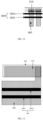
- FIG. 1 is a schematic structural diagram of a display substrate according to an embodiment of the present disclosure.
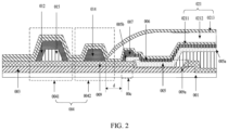
- FIG. 2 is a sectional view of the display substrate shown in FIG. 1 taken along a direction of BB.
- the display substrate may be a flexible panel, and may be, for example, a foldable panel.
- the display substrate may include: a base substrate 001, a plurality of pixel units 002, at least one first power line 003, a blocking structure 004, an auxiliary connection structure 005, a cathode layer 006 and a first organic pattern 007.
- the plurality of pixel units 002 may be located on the base substrate 001.
- the auxiliary connection structure 005 the cathode layer 006 is not shown in FIG. 1 .
- the at least one first power line 003 is located on the base substrate 001.
- the blocking structure 004 surrounds the plurality of pixel units 002.
- the auxiliary connection structure 005 includes a first side surface 005a and a second side surface 005b which are opposite to each other, and the first side surface 005a is closer to the plurality of pixel units 002 than the second side surface 005b is.
- the cathode layer 006 is located on a side of the auxiliary connection structure 005 distal from the base substrate 001.
- the first organic pattern 007 is located on the side of the auxiliary connection structure 005 distal from the base substrate 001.
- One end 003a of the at least one first power line 003 is located on a side of the blocking structure (the dam structure) 004 distal from the plurality of pixel units 002 and is configured for receiving a power signal.
- the other end 003b of the at least one first power line 003 is located between the blocking structure 004 and the plurality of pixel units 002 and is connected with the cathode layer 006 through the auxiliary connection structure 005, thereby enabling the first power line 003 to provide the power signal to the cathode layer 006.
- each first power line 003 is located outside a region surrounded by the blocking structure (the dam structure) 004, and the other end is located within the region surrounded by the blocking structure 004, i.e., each first power line 003 can pass through the blocking structure 004 to enter the region surrounded by the blocking structure 004.
- the portion of the blocking structure 004 configured for allowing the power line to pass through can also be referred to as a line inlet port.
- the portion allowing the first power line 003 to pass through may be referred to as a first line inlet port 00a.
- first power lines 003 are illustrated in FIG. 1 , and the end 003a of each first power line 003 is connected with a driving chip for receiving the power signal provided by the driving chip.
- FIG. 3 is a schematic structural diagram of another display substrate according to an embodiment of the present disclosure.
- FIG. 4 is a local schematic structural diagram of a display substrate according to an embodiment of the present disclosure.
- an orthographic projection of the auxiliary connection structure 005 on the base substrate 001 includes a first projection region 005c and a second projection region 005d.
- the first projection region 005c is closer to the end 003a of the at least one first power line 003 for receiving the power signal than the second projection region 005d is.
- the first projection region 005c and an orthographic projection of the blocking structure 004 on the base substrate 001 do not overlap; and the second projection region 005d and the orthographic projection of the blocking structure 004 on the base substrate 001 overlap to form a region including a first overlapping region 00b.
- the first power line 003, a second power line 008 and the cathode layer 006 are not shown in FIG. 3 .
- a first organic pattern 007 may be generally configured to cover at least a part of the second side surface 005b, thereby guaranteeing that the auxiliary connection structure 005 can effectively transmit the power signal from the first power line 003.
- the organic material for manufacturing the first organic pattern 007 is a hydrophilic material, therefore, by disposing the first projection region 005c formed from the orthographic projection of the auxiliary connection structure 005 on the base substrate 001 as not overlapping with the orthographic projection of the blocking structure 004 on the base substrate 001, the first organic pattern 007 is configured to be not in contact with the blocking structure 004 when it covers at least a part of the second side surface 005a of the auxiliary connection structure 005 at the first projection region 005c, i.e., the first organic pattern 007 is configured to be spaced apart from the blocking structure 004; and therefore, the moisture brought in by the end 003a of the first power line 003 for receiving the power signal can be prevented from being further introduced into the plurality of pixel units 002 through the blocking structure 004 and the first organic pattern 007, thereby guaranteeing the yield of the display substrate.
- the width of a lap joint between the auxiliary connection structure 005 and the first power line 003 can be relatively wide, so as to guarantee that the contact resistance between the auxiliary connection structure 005 and the first power line 003 is as small as possible.
- an orthographic projection of the lap joint on the base substrate is an area where the first projection region 005c and the orthographic projection of the first power line 003 on the base substrate 001 overlap.
- the width of other portions of the auxiliary connection structure 005 distal from the lap joint may be narrow, so as to reduce the capacitive coupling effect on other signal lines provided on the side of the auxiliary connection structure 005 proximal to the base substrate. For example, the capacitive coupling effect on the data lines can be reduced.
- the embodiments of the present disclosure provide a display substrate, which includes a base substrate, a plurality of pixel units, at least one first power line, a blocking structure, an auxiliary connection structure, a cathode layer and a first organic pattern.
- a first projection region of an orthographic projection of the auxiliary connection structure on the base substrate and an orthographic projection of the blocking structure on the base substrate do not overlap, such that the first organic pattern is spaced apart from the blocking structure; and therefore, the moisture brought in by one end of the first power line for receiving a power signal can be prevented from being introduced into the pixel units through the blocking structure and the first organic pattern, thereby guaranteeing the yield of the display substrate, as well as the display effect of the display substrate.
- the region where the orthographic projections of the plurality of pixel units 002 on the base substrate 001 are located may be an active area (AA) of the display substrate, also known as a display region or an AA region. Therefore, the blocking structure 004 is disposed to surround the AA region.
- the cathode layer 006 may form an entire layer to cover the AA region.
- the orthographic projection of the cathode layer 006 on the base substrate 001 may cover the orthographic projections of the plurality of pixel units 002 on the base substrate 001; and the orthographic projection of the cathode layer 006 on the base substrate 001 may be inside the orthographic projection of the region surrounded by the blocking structure 004 on the base substrate 001.
- the first organic pattern 007 may cover at least a portion of the second side surface 005b of the auxiliary connection structure 005; an orthographic projection of the first organic pattern 007 and the orthographic projection of the at least one first power line 003 on the base substrate 001 overlap at a second overlapping region 00c, and the second overlapping region 00c and the orthographic projection of the blocking structure 004 on the base substrate 001 do not overlap.
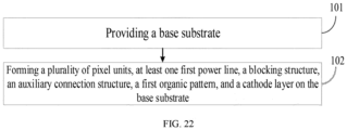
- the risk of the second side surface of the auxiliary connection structure 005 being eroded by moisture or oxygen due to the etching defect can be reduced, thereby guaranteeing that the auxiliary connection structure 005 can effectively transmit the power signal from the first power line 003.
- the organic material for manufacturing the first organic pattern 007 is typically a hydrophilic material, therefore, by disposing the second overlapping region 00c as not overlapping with the orthographic projection of the blocking structure 004 on the base substrate, i.e., making the first organic pattern 007 be spaced apart from the blocking structure 004, the moisture brought in by the end 003a of the first power line 003 for receiving the power signal can be prevented from being introduced into the pixel unit 002 through the blocking structure 004 and the first organic pattern 007, thereby guaranteeing the yield of the display substrate.
- a distance between the second overlapping region 00c, where the orthographic projection of the first organic pattern 007 and the orthographic projection of the at least one first power line 003 on the base substrate 001 overlap, and the orthographic projection of the blocking structure 004 on the base substrate 001 may be greater than a threshold distance.
- the threshold distance may be in a range from 80 microns( ⁇ m) to 150 ⁇ m.
- the threshold distance may be 90 ⁇ m, 100 ⁇ m, 110 ⁇ m, 120 ⁇ m, 130 ⁇ m, 140 ⁇ m, etc. That is, a certain distance is presented between the first organic pattern 007 and the blocking structure 004.
- the first organic pattern 007 can be prevented from directly contacting the blocking structure 004 near the first line inlet port 00a of the first power line 003, and the moisture can be further prevented from being introduced into the pixel unit 002 through the first organic pattern 007, thereby guaranteeing the encapsulation effect.
- the threshold distance may be a threshold that is determined in advance through experiments as being able to prevent the moisture from entering the pixel units 002. That is, when the distance between the second overlapping region 00c and the blocking structure 004 is greater than the threshold distance, it is hard for the moisture to enter the pixel units 002 in the display substrate.
- the threshold distance may be a threshold that is determined in advance through experiments as being able to prevent the moisture from entering the pixel units 002. That is, when the distance between the second overlapping region 00c and the blocking structure 004 is greater than the threshold distance, the moisture would not enter the pixel units 002 in the display substrate.
- the second side surface 005b of the auxiliary connection structure 005 may also be covered by the blocking structure 004. That is, the second side surface 005b of the auxiliary connection structure 005 in the second projection region 005d may be covered by the blocking structure 004.
- the area of the base substrate 001 occupied by the auxiliary connection structure 005 and the blocking structure 004 can be reduced, facilitating the realization of a narrow-frame display substrate.
- the second projection region 005d of the auxiliary connection structure 005 has a longer distance from the first portion 0081 of the at least one second power line 008. Referring to FIG. 6 , at a position distal from a second line inlet port 00d, a long entrance path is formed for the moisture, even if the second side surface 005b of the auxiliary connection structure 005 is covered by the blocking structure 004, the moisture cannot enter the pixel units 002.
- the auxiliary connection structure 005 may be in a ring construction surrounding the plurality of pixel units 002, so as to facilitate the cathode layer 006 to be connected to the at least one first power line 003 through the auxiliary connection structure 005, thereby guaranteeing the uniformity of potential of the power signal provided to the pixel units 002 of the display substrate, and achieving a good display effect.
- the end 003a of the at least one first power line 003 may be located in a middle of the side of the blocking structure 004 distal from the plurality of pixel units 002, for example, in the middle of the bonding region 00e.
- the middle is a position where the longitudinal axis X of the base substrate passes through, and the longitudinal axis X is an axis parallel to the data line on the base substrate 001.
- a distance between the longitudinal axis X and one side of the display substrate is approximately equal to a distance between the longitudinal axis X and the other side of the display substrate.
- the one side and the other side are approximately parallel to an extension direction of the data line. For example, an included angle between any one of the two sides of the display substrate approximately parallel to the extension direction of the data line and the extension direction of the data line ranges from 0 degree to 10 degrees.
- “approximately” in the embodiments of the present disclosure refers to that an error range within 15% is allowed. If the distances are “approximately” equal to each other, then a difference between the two distances is no more than 15%. If the extension directions are “approximately” parallel to each other, then the included angle of the two extension directions is between 0 degree and 30 degrees, such as 0 degree to 10 degrees, 0 degree to 15 degrees and so on. If the shapes are “approximately” the same with each other, then the two shapes are of the same type, such as a rectangle, a polyline, an arc, a strip, an "L” type and so on. If the areas are “approximately” the same, then a difference between the two areas does not exceed 15%, etc.
- the display substrate may include two first power lines 003.
- the two first power lines 003 may be adjacently arranged in the middle of the side of the blocking structure 004 distal from the plurality of pixel units 002.
- the two first power lines 003 are arranged in the middle of the side of the blocking structure 004 away from the plurality of pixel units 002, and are spaced from each other to be symmetrical with each other with respect to the longitudinal axis X of the base substrate as a symmetric axis.
- the arranging positions of the first power lines 003 are not limited in the embodiment of the present disclosure.
- the two first power lines 003 When the two first power lines 003 are adjacently arranged in the middle of the side of the blocking structure 004 distal from the plurality of pixel units 002, the two first power lines 003 may be formed to be a structure formed integrally.
- the two first power lines 003 are formed integrally, that is, when there is one first power line 003, one end 003a of the first power line 003 is located in the middle of the side of the blocking structure 004 distal from the plurality of pixel units 002, for example, located in the middle of the bonding region 00e, so that the distance from the end 003a of the first power line 003 to the longitudinal axis X is less than the distance from the end 003a of the first power line 003 to any side of the two sides approximately parallel to the longitudinal axis X of the display substrate.
- a folding line of the foldable panel may be perpendicular to the longitudinal axis X.
- the folding line of the foldable panel may be a perpendicular bisector of the longitudinal axis X.
- the display substrate further includes: at least one second power line 008.
- the at least one second power line 008 includes a first portion 0081 and a second portion 0082.
- the first portion 0081 is located on the side of the blocking structure 004 distal from the plurality of pixel units 002, and is configured for receiving a power signal.
- the first portion 0081 may be connected with a driving chip and configured for receiving a power signal provided by the driving chip.
- the second portion 0082 is connected with the cathode layer 006 through the auxiliary connection structure 005.
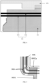
- FIG. 5 is a local schematic structural diagram of the display substrate shown in FIG. 1 .
- the second portion 0082 includes a first junction 0082a and a second junction 0082b which are both connected with the blocking structure 004, and a distance between the first junction 0082a and the blocking structure 004 is greater than a distance between the second junction 0082b and the blocking structure 004. That is, the first junction 0082a of the second portion 0082 of the at least one second power line 008 is not in contact with the blocking structure 004.
- an orthographic projection of the first junction 0082a on the base substrate 001 and an orthographic projection of the blocking structure 004 on the base substrate 001 do not overlap; and the second junction 0082b may be located within a region covered by the blocking structure 004, for example, the second junction 0082b may be in contact with the blocking structure 004.
- the display substrate may further have a bonding region 00e, which may be located on the side of the blocking structure distal from the plurality of pixel units 002.
- the first junction 0082a is closer to the bonding region 00e than the second junction 0082b is.
- “being closer” means that the shortest distance between the respective points of the first junction 0082a and the bonding region 00e is greater than the shortest distance between the respective points of the second junction 0082b and the bonding region 00e.
- each junction of the first junction 0082a and the second junction 0082b refers to: a portion of the second portion 0082 of the second power line 008 which is in contact with the auxiliary connection structure 005.
- the junction refers to a portion of the second portion 0082 which is in direct contact with the auxiliary connection structure 005.
- the shapes of the two junctions may be substantially the same as the shape of the region where the orthographic projection of the second portion 0082 on the base substrate 001 and the orthographic projection of the auxiliary connection structure 005 on the base substrate 001 overlap.
- the second power line 008 may include two first portions 0081.
- the two first portions 0081 may be substantially symmetrically disposed, with respect to the longitudinal axis X of the base substrate 001, around an edge of a side of the blocking structure 004 distal from the plurality of pixel units 002.
- the second power line 008 may include two first portions 0081.
- the two first portions 0081 may be located on two sides of the longitudinal axis X respectively, such as at two sides of the bonding region 00e.
- the second power line 008 may include two first portions 0081.
- the part of the two first portions 0081 which are near the second line inlet port 00d are respectively located at two sides of the display substrate, in another example, respectively proximal to two side edges that are parallel to the longitudinal axis X.
- the second line inlet port 00d may be a portion of the blocking structure 004 for allowing the second power line 008 to pass through.
- Both the first power line 003 in the middle and the second power line 008 at the edge provide the power signal to the cathode layer 006 in the display substrate at the same time, so as to further alleviate the problem that a potential difference of the power signal loaded to the cathode layers 006 in different regions is large due to voltage drop.
- the cathode layer 006 has good long range uniformity (LRU) and an improved display effect.
- Both the first power line 003 in the middle and the second power line 008 at the edge provide the power signal to the cathode layer 006 in the display substrate.
- the design of the first power line 003 in the embodiments of the present disclosure can favorably mitigate the moisture and oxygen erosions and guarantee a good encapsulation performance.
- more first power lines 003 may be provided.
- the uniformity of potential in respective regions of the cathode layer 006 can be guaranteed and the display substrate can achieve an improved display effect.
- both the first power line 003 and the second power line 008 are configured to provide the power signal to the cathode layer 006, both the first power line 003 and the second power line 008 may be referred to as a VSS power line or a VSS wire.
- the display substrate may further include: a row driving region 00f located between the blocking structure 004 and the plurality of pixel units 002.
- a distance between the row driving region 00f and the orthographic projection of the at least one first power line 003 on the base substrate 001 may be greater than a distance between the row driving region 00f and the orthographic projection of the at least one second power line 008 on the base substrate.
- the distance between the at least one first power line 003 located in the middle and the row driving region 00f may be longer than the distance between the at least one second power line 008 and the row driving region 00f.
- the shortest distance between respective portions of each first power line 003 and the row driving region 00f is greater than the shortest distance between respective portions of each second power line 008 and the row driving region 00f.
- the distance h1 between a point a1 of the at least one first power line 003 and the row driving region 00f is greater than the distance h2 between a point b1 of the at least one second power line 008 and the row driving region 00f.
- the row driving region 00f may be provided with a plurality of cascaded shift register units, which may be configured to drive each row of the pixel units 002.
- the display substrate may have two row driving regions 00f, which are respectively arranged on two sides of the plurality of pixel units 002 and are symmetrically arranged with the longitudinal axis X of the base substrate 001 as the symmetrical axis.
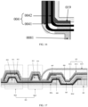
- the display substrate may further include: a passivation layer 009 which may cover the at least one first power line 003.
- FIG. 7 is a local schematic structural diagram of another display substrate according to an embodiment of the present disclosure. Referring to FIGS. 2 and 7 , the passivation layer 009 is further provided with an opening 009a; a side of the auxiliary connection structure 005 proximal to the base substrate 001 is connected with the at least one first power line 003 through the opening 009a, and a side of the auxiliary connection structure 005 distal from the base substrate 001 is connected with the cathode layer 006.
- the reference 009a shown in FIG. 7 is an opening provided in the passivation layer 009. That is, in FIG. 7 , except the region where the opening 009a is located, all other regions are covered by the passivation layer 009.
- the at least one first power line 003 is easy to be eroded by moisture or oxygen during the manufacturing of the display substrate, by covering the at least one first power line 003 with the passivation layer 009, it can be guaranteed that when other layers are formed subsequently, the at least one first power line 003 would not be eroded by moisture or oxygen, thereby guaranteeing that the at least one first power line 003 can provide the power signal to the cathode layer 006, so as to ensure the display effect of the display substrate.
- the opening in the passivation layer 009 may be a via hole or may be a slot, which is not limited in the embodiments of the present disclosure.
- the material for manufacturing the passivation layer 009 may include: one or more of inorganic oxides such as SiNx (silicon nitride), SiOx (silicon oxide) and SiOxNy (silicon oxynitride). The material for manufacturing the passivation layer 009 is not limited by the embodiments of the present disclosure.
- the passivation layer 009 may further cover the at least one second power line 008, thereby guaranteeing that the at least one second power line 008 would not be eroded by moisture or oxygen, so as to ensure the display effect of the display substrate.
- the blocking structure 004 is in a ring construction surrounding the plurality of pixel units 002 to block the overflow of an organic layer in the region surrounded by the blocking structure 004 of the display substrate.
- the blocking structure 004 may include: a first blocking dam 0041 and a second blocking dam 0042.
- the first blocking dam 0041 is farther away from the plurality of pixel units 002 than the second blocking dam 0042 is, and the thickness of the first blocking dam 0041 is greater than the thickness of the second blocking dam 0042.
- the blocking structure 004 may further include one blocking dam, or more than two blocking dams, which is not limited in the embodiments of the present disclosure.
- FIG. 8 is a schematic structural diagram of still another display substrate according to an embodiment of the present disclosure.
- the first blocking dam 0041 may include: a first planarization layer pattern 010, a second planarization layer pattern 011 and a second organic pattern 012 which are disposed along a direction away from the base substrate 001.
- the second blocking dam 0042 may include: a third planarization layer pattern 013 and a third organic pattern 014 which are arranged along a direction away from the base substrate 001.
- the second planarization layer pattern 011 and the third planarization layer pattern 013 may include a same material; and the first organic pattern 007, the second organic pattern 012 and the third organic pattern 014 may include a same material.
- the second planarization layer pattern 011 and the third planarization layer pattern 013 may employ the same material and may be prepared from a same patterning process; and the first organic pattern 007, the second organic pattern 012 and the third organic pattern 014 may employ the same material and may be prepared from a same patterning process.
- the first planarization layer pattern 010 may belong to the first planarization layer; the second planarization layer pattern 011 and the third planarization layer pattern 013 may belong to the second planarization layer; and the first organic pattern 007, the second organic pattern 012 and the third organic pattern 014 may belong to the first organic layer which may be a pixel definition layer (PDL).
- PDL pixel definition layer
- the materials for manufacturing the first planarization layer, the second planarization layer and the first organic layer may include: organic materials such as resins. This is not limited in the embodiments of the present disclosure.
- the first blocking dam 0041 may include: a planarization lay er pattern 015 and a second organic pattern 012 which are sequentially arranged in layers along a direction away from the base substrate 001.
- the second blocking dam 0042 may include: a third organic pattern 014 disposed on the base substrate 001.
- the first organic pattern 007, the second organic pattern 012 and the third organic pattern 014 may include a same material.
- the first organic pattern 007, the second organic pattern 012 and the third organic pattern 014 may employ the same material and may be prepared from a same patterning process.
- the planarization layer pattern 015 may belong to the planarization layer; and the first organic pattern 007, the second organic pattern 012 and the third organic pattern 014 may belong to the first organic layer.
- the materials for manufacturing the planarization layer may include: organic materials such as resins. This is not limited in the embodiments of the present disclosure.
- the opening 015a shown in FIG. 7 is a region not covered by the planarization layer pattern 015.
- the planarization layer pattern 015 may cover a boundary of a portion of the first power line 003 located in the region surrounded by the blocking structure 004.
- the region where the overlapping region and the orthographic projection of the opening 009a of the planarization layer 009 on the base substrate 001 overlap may cover the region where the overlapping region and the orthographic projection of the opening 015a of the planarization layer pattern 015 on the base substrate 001 overlap. That is, in the overlapping region, the size of the opening 009a of the planarization layer 009 is greater than the size of the opening 015a of the planarization layer pattern 015.
- the first blocking dam 0041 has one more planarization layer pattern than the second blocking dam 0042, so that the thickness of the first blocking dam 0041 is greater than the thickness of the second blocking dam 0042, which prevents the overflow of the organic layer.
- FIG. 9 is a schematic structural diagram of still another display substrate according to an embodiment of the present disclosure.
- the first blocking dam 0041 may further include: a fourth organic pattern 016 disposed on a side of the second organic pattern 012 distal from the base substrate 001.
- the second blocking dam 0042 may further include: a fifth organic pattern 017 disposed on a side of the third organic pattern 014 distal from the base substrate 001.
- the fourth organic pattern 016 and the fifth organic pattern 017 may include a same material.
- the fourth organic pattern 016 and the fifth organic pattern 017 may employ the same material and may be prepared from a same patterning process.
- both the fourth organic pattern 016 and the fifth organic pattern 017 may belong to the second organic layer, which may be a photo spacer (PS).
- PS photo spacer
- the materials for manufacturing the second organic layer may include: organic materials such as resins. This is not limited in the embodiments of the present disclosure.
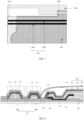
- FIG. 10 is a schematic structural diagram of still another display substrate according to an embodiment of the present disclosure.
- the first organic pattern 007 may cover the second side surface 005b of the auxiliary connection structure 005.
- the first blocking dam 0041 may be a first ring
- the second blocking dam 0042 may be a second ring.
- the first organic pattern 007 and a portion of the third organic pattern 014 may define a third ring.
- An orthographic projection of the third ring on the base substrate 001 may be located inside an orthographic projection of the second ring on the base substrate 001, and the orthographic projection of the second ring on the base substrate 001 may be located inside an orthographic projection of the first ring on the base substrate 001.
- the third ring may surround the plurality of pixel units 002.
- the shape of the third organic pattern 014 may be substantially the same as that of the second blocking dam 0042, that is, the third organic pattern 014 may also be ring-shaped.
- the portion of the third organic pattern 014 may be a portion of the third organic pattern 014 located on the side of the first organic pattern 007 proximal to the plurality of pixel units 002.
- the portion of the third organic pattern 014 may be the left portion, the upper portion, and the right portion of the third organic pattern 014.
- the first organic pattern 007 may include a portion which is in direct contact with the second blocking dam 0042.
- the second power line 008 may include two first portions 0081 and one second portion 0082.
- the two first portions 0081 may be symmetrically disposed on two sides of the base substrate 001 with respect to the longitudinal axis X of the base substrate 001.
- the part of the two first portions 0081 near the second line inlet port 00d may be located on two sides of the display substrate, and in another example, may be respectively located close to each of the two side edges that are parallel to the longitudinal axis X.
- FIG. 6 shows the second line inlet port 00d of the two first portions 0081.
- the second portion 0082 may surround the plurality of pixel units 002, and the two ends of the second portion 0082 may be connected with one first portion 0081 respectively.
- first portion 0081 and the second portion 0082 may be in direct contact, for example, may be formed integrally.
- the second power line 008 may include: a straight portion 0082c and an arc-shaped portion 0082d which surround a region where the plurality of pixel units 002 are located.
- the second portion 0082 may include: a straight portion 0082c and an arc-shaped portion 0082d which surround a region where the plurality of pixel units 002 are located. Furthermore, the second portion 0082 of the second power line 008 may include a non-enclosed structure. The embodiments of the present disclosure take the second portion 0082 at least surrounding two edges of the display substrate as an example for description. An orthographic projection of a portion, in direct contact with the second blocking dam 0042, of the first organic pattern 007 on the base substrate 001 may be located within an orthographic projection of the arc-shaped portion 0082d on the base substrate 001.
- the orthographic projection of the portion, which is in direct contact with the second blocking dam 0042, of the first organic pattern 007 on the base substrate 001 does not go outside of the orthographic projection of the arc-shaped portion 0082d on the base substrate 001.
- the arc-shaped portion 0082d is closer to the first portion 0081 of the at least one second power line 008 for receiving the power signal than the straight portion 0082c is.
- the at least one first power line 003 may include: a first metal layer 003c.
- the display substrate may further include: an auxiliary metal layer 018 on a side of the first metal layer 003c distal from the base substrate 001.
- a side of the auxiliary metal layer 018 distal from the first metal layer 003c may be in contact with the auxiliary connection structure 005, and an orthographic projection of the auxiliary metal layer 018 on the base substrate 001 and the orthographic projection of the blocking structure 004 on the base substrate 001 do not overlap.
- the orthographic projection of the auxiliary metal layer 018 on the base substrate 001 includes a portion which is within a region surrounded by the orthographic projection of the blocking structure 004 on the base substrate 001.
- FIG. 12 is a local schematic structural diagram of still another display substrate according to an embodiment of the present disclosure.
- the orthographic projection of the auxiliary metal layer 018 on the base substrate 001 includes a portion which is within a region surrounded by the orthographic projection of the second blocking structure 0042 on the base substrate 001.
- the side of the first metal layer 003c distal from the base substrate 001 is not provided with the auxiliary metal layer 018 in the region where the blocking structure 004 is located. That is, in the region where the blocking structure 004 is located, the auxiliary metal layer 018 is removed. That is, in the region where the first line inlet port 00a is located, the auxiliary metal layer 018 is removed.
- the side of the blocking structure 004 distal from the plurality of pixel units 002 may be provided with an auxiliary metal layer 018; and the region surrounded by the blocking structure 004 may also be provided with an auxiliary metal layer 018.
- the shape of a boundary of the auxiliary metal layer 018 may be substantially the same as the shape of a boundary of the first metal layer 003c, or the shape of the boundary of the auxiliary metal layer 018 may also be different from the shape of the boundary of the first metal layer 003c. This is not limited in the embodiments of the present disclosure.
- the power signal received by the first metal layer 003c may be transmitted to the auxiliary connection structure 005 through the auxiliary metal layer 018 disposed in the opening of the passivation layer 009.
- the power signal is transmitted to the cathode layer 006 through the auxiliary connection structure 005.
- the side of the auxiliary metal layer 018 distal from the base substrate 001 may be covered, at portions close to the edges and at the side edges, by a second planarization layer including the second planarization layer pattern 011 and the third planarization layer pattern 013; and the second planarization layer can be configured to avoid display defects caused by etching defects on the sidewalls of the auxiliary metal layer 018.
- the organic material for manufacturing the second planarization layer is typically a hydrophilic material, therefore, in order to prevent the auxiliary metal layer 018 from introducing moisture into the pixel units 002, the orthographic projection of the auxiliary metal layer 018 on the base substrate 001 and the orthographic projection of the blocking structure 004 on the base substrate 001 can be configured to have no overlapped region, such that the moisture can be prevented from entering inside from the blocking structure 004 and entering the region where the pixel units 002 are located along the path formed by the second planarization layer, thereby guaranteeing the display effect of the display substrate.
- FIG. 13 is a local schematic structural diagram of still another display substrate according to an embodiment of the present disclosure.
- the orthographic projection of a portion of the auxiliary metal layer 018 in contact with the first metal layer 003c, on the base substrate 001 may be located within the orthographic projection of the auxiliary metal layer 018 on the base substrate 001, so that a distance is presented between the boundary of the first metal layer 003c and the boundary of the auxiliary metal layer 018.
- the first metal layer 003c and the auxiliary metal layer 018 can be prevented from being eroded by the moisture or oxygen.
- FIG. 14 is a local schematic structural diagram of still another display substrate according to an embodiment of the present disclosure. The reference 010a shown in FIG.
- FIG. 14 illustrates an opening provided in the first planarization layer. That is, in FIG. 14 , except the region where the opening 010a is located, all other regions are covered with the first planarization layer.
- the reference 011a shown in FIG. 14 illustrates an opening provided in the second planarization layer. That is, in FIG. 14 , except the region where the opening 011a is located, all other regions are covered with the second planarization layer.
- the first metal layer 003c, the passivation layer 009, the first planarization layer pattern 010, the auxiliary metal layer 018, the second planarization layer pattern 011 and the first organic pattern 007 of the display substrate may be arranged in layers along a direction away from the base substrate 001. That is, the first power line 003, the passivation layer 009, the first planarization layer, the auxiliary metal layer 018, the second planarization layer and the first organic layer of the display substrate may be arranged in layers along the direction of the base substrate 001.
- both the first metal layer 003c and the auxiliary metal layer 018 may include three metal film layers.
- the materials of the three metal film layers may sequentially be: titanium (Ti), aluminum (Al) and Ti.
- FIG. 15 is a sectional view of the display substrate shown in FIG. 1 taken along a direction of CC.
- the at least one second power line 008 may include: a second metal layer 008a.
- the display substrate may further include: an auxiliary wiring layer 019 on a side of the second metal layer 008a distal from the base substrate 001.
- a side of the auxiliary wiring layer 019 distal from the second power line 008 is in contact with the auxiliary connection structure 005, and an orthographic projection of the auxiliary wiring layer 019 on the base substrate 001 and the orthographic projection of the blocking structure 004 on the base substrate 001 does not overlap.
- the orthographic projection of the auxiliary wiring layer 019 on the base substrate 001 may include a portion which is within the orthographic projection of the blocking structure 004 on the base substrate 001.
- FIG. 16 is a local schematic structural diagram of still another display substrate according to an embodiment of the present disclosure.
- the orthographic projection of the auxiliary wiring layer 019 on the base substrate 001 may have a portion which is within the orthographic projection of the second blocking structure 0042 on the base substrate 001.
- the side of the second metal layer 008a distal from the base substrate 001 is not provided with the auxiliary wiring layer 019 in the region where the blocking structure 004 is located. That is, in the region where the blocking structure 004 is located, the auxiliary wiring layer 01 is removed. That is, in the region where the second line inlet port 00d is located, the auxiliary wiring layer 019 is removed.
- the side of the blocking structure 004 distal from the plurality of pixel units may be provided with the auxiliary wiring layer 019; and the region included in the blocking structure 004 may be provided with the auxiliary wiring layer 019.
- the shape of a boundary of the auxiliary wiring layer 019 may be substantially the same as the shape of a boundary of the second metal layer 008a, or the shape of the boundary of the auxiliary wiring layer 019 may be different from the shape of the boundary of the second metal layer 008a. This is not limited in the embodiments of the present disclosure.
- the at least one first power line 003 may include: a first metal layer 003c and a third metal layer 003d which are disposed along a direction away from the base substrate 001. A side of the third metal layer 003d distal from the first metal layer 003c is in contact with the auxiliary connection structure 005.
- Both the orthographic projection of the first metal layer 003c on the base substrate 001 and the orthographic projection of the third metal layer 003d on the base substrate 001 may overlap with the orthographic projection of the blocking structure 004 on the base substrate 001. That is, the ends of both the first metal layer 003c and the third metal layer 003d distal from the plurality of pixel units 002 can be configured to receive the power signal, so that the power signal can be transmitted to the cathode layer 006 through both the first metal layer 003c and the third metal layer 003d. Therefore, the resistance can be reduced and the voltage drop of the power signal can be further reduced.
- the orthographic projection of the first metal layer 003c on the base substrate 001 and the region where the third metal layer 003d is in contact with the auxiliary connection structure 005 do not overlap.
- the orthographic projection of the first metal layer 003c on the base substrate 001 may overlap with the region where the third metal layer 003d is in contact with the auxiliary connection structure 005.
- the first planarization layer may cover the other end of the first metal layer 003c proximal to the plurality of pixel units 002, so as to reduce the oxygen or moisture corrosions occurring on the other end of the first metal layer 003c, or to reduce the final display defects caused by the etching defects of the side surfaces of the metal layers.
- the first metal layer 003c, the first planarization layer pattern 010, the third metal layer 003d, the passivation layer 009, the second planarization layer pattern 011 and the first organic pattern 007 of the display substrate may be arranged in layers along a direction away from the base substrate 001. That is, the first metal layer 003c, the first planarization layer, the third metal layer 003d, the passivation layer 009, the second planarization layer, and the first organic layer of the display substrate may be arranged in layers along the direction of the base substrate 001.
- both the first metal layer 003c and the third metal layer 003d may include three metal film layers.
- the materials of the three metal film layers may sequentially be: Ti, Al and Ti.
- the first blocking dam 0041 further includes a fourth organic pattern 016 disposed on a side of the second organic pattern 012 distal from the base substrate
- the second blocking dam 0042 further includes a fifth organic pattern 017 disposed on a side of the third organic pattern 014 distal from the base substrate 001
- the second organic layer including the fourth organic pattern 016 and the fifth organic pattern 017 can be disposed on a side of the first organic layer distal from the base substrate 001.
- FIG. 19 is a schematic structural diagram of still another display substrate according to an embodiment of the present disclosure.
- a plurality of tooth-shaped protruding structures are formed on a side surface of the at least one first power line 003 located on the side of the blocking structure 004 distal from the plurality of pixel units 002. Therefore, an entrance path of moisture can be further prolonged, and the moisture can be prevented from being introduced into the plurality of pixel units 002.
- orthographic projections of the protruding structures on the base substrate 001 and the orthographic projection of the blocking structure 004 on the base substrate 001 do not overlap.
- a side surface of the other end 003b of the at least one first power line 003 within the region surrounded by the blocking structure 004 may be flat. That is, no protruding structure is formed on the side surface of the other end 003b of the at least one first power line 003 within the region surrounded by the blocking structure 004.
- the auxiliary connection structure 005 is obtained by sequential processes such as exposure, development, etching and other processes. In the etching process, an etchant is needed for etching a film layer. If the side surface of the other end 003b of the first power line 003 within the region surrounded by the blocking structure 004 is also configured to have tooth-shaped protruding structures, the etchant will be retained among the adjacent protruding structures of the first power line 003, so that the sidewall of the other end 003b of the first power line 003 will be corroded.
- the passivation layer 009 which is a brittle film on the side of the first power line 003 distal from the base substrate 001 can be prevented from being penetrated through, due to the corrosion on the sidewall of the first power line 003, in the process of manufacturing the display substrate.
- the quality of the passivation layer 009 can be guaranteed.
- a plurality of tooth-shaped protruding structures may also be formed on a side surface of an end, distal from the plurality of pixel units 002, of a first portion 0081 of the at least one second power line 008. Therefore, an entrance path of moisture along the second power line 008 can be prolonged, and the moisture can be prevented from being introduced into the plurality of pixel units 002. Furthermore, the side surface of the other end, within the region surrounded by the blocking structure 004, of the first portion 0081 of the at least one second power line 008 may be flat.
- the display substrate may further include: a plurality of third power lines 020, which may be located on the base substrate 001.
- the plurality of third power lines 020 are electrically connected with transistors in the pixel units 002 of the display substrate.
- the third power lines 020 may be respectively connected with a source electrode or a drain electrode of the transistors in the pixel units 002.
- the third power line 020 may be configured to provide a positive power signal to the transistor in the pixel units 002, such that the third power lines 020 may also be referred to as VDD power lines or a VDD wires.
- the plurality of third power lines 020 may be symmetrically disposed on two sides of the at least one first power line 003.
- the display substrate may include: four third power lines 020.
- two of the third power lines 020 may be located in the middle of the side of the blocking structure 004 distal from the plurality of pixel units 002; and the two third power lines 020 may be symmetrically disposed on two sides of the first power line 003 with respect to the longitudinal axis X of the base substrate 001.
- the remaining two third power lines 020 may be both located at an edge of the side of the blocking structure distal from the plurality of pixel units 002.
- Each third power line 020 may be located on the side of one first portion 0081 of the second power line 008 proximal to the first power line 003.
- a plurality of tooth-shaped protruding structures may also be formed on side surfaces of the ends of the plurality of third power lines 020 that are located on the side of the blocking structure 004 distal from the plurality of pixel units 002, so that the paths of introducing moisture along the third power lines 020 are extended to avoid moisture from being introduced into the plurality of pixel units 002.
- the side surface of the other end of each of the third power lines 020 that is within the region surrounded by the blocking structure 004 may be flat.
- the display substrate may further include: an encapsulation film layer 021.
- the encapsulation film layer 021 may be located on a side of the plurality of first power lines distal from the base substrate 001, and the encapsulation film layer 021 may cover the region surrounded by the blocking structure 004.
- the encapsulation film layer 021 may include: a first film layer 0211, a second film layer 0212 and a third film layer 0213 disposed in layers in a direction away from the base substrate 001.
- the first film layer 0211 and the third film layer 0213 may be made of inorganic materials, and the second film layer 0212 may be made of an organic material.
- the first film layer 0211 and the third film layer 0213 may be made of one or more inorganic oxides such as SiNx, SiOx and SiOxNy.
- the second film layer 0212 may be made of a resin material.
- the resin material may be thermoplastic resin or a thermosetting resin.
- the thermoplastic resin may include acrylic (PMMA) resins, and the thermosetting resin may include epoxy resins.
- the second film layer 0212 may be located within the region surrounded by the blocking structure 004, and the first film layer 0211 and the third film layer 0213 may cover the region surrounded by the blocking structure 004 and further cover the blocking structure 004. That is, the orthographic projection of the blocking structure 004 on the base substrate 001 may be located within the region covered by the encapsulation film layer 021. As such, the encapsulation film layer 021 is ensured to effectively encapsulate respective structures located in the region surrounded by the blocking structure 004.
- FIG. 20 is a schematic structural diagram of still another display substrate according to an embodiment of the present disclosure.
- a buffer layer 022, a semiconductor layer 023, a gate insulating layer 024, a gate electrode 025, an interlayer dielectric layer 026 and a source-drain electrode layer 027 may be sequentially disposed on the base substrate 001; and the source-drain electrode layer 027 may include a source electrode 0271 and a drain electrode 0272.
- the source electrode 0271 and the drain electrode 0272 are spaced apart from each other, and may be connected with the semiconductor layer 023 through via holes, respectively.
- FIG. 21 is a schematic structural diagram of still another display substrate according to an embodiment of the present disclosure.
- the orthographic projections of the plurality of third power lines 020 on the base substrate 001 may have an overlapping region with the orthographic projection of the auxiliary connection structure 005 on the base substrate 001.
- the passivation layer 009 may be provided between the plurality of third power lines 020 and the auxiliary connection structure 005.
- the plurality of third power lines 020 are not in contact with the auxiliary connection structure 005.
- the at least one first power line 003 may be first formed on the base substrate 001, and then the blocking structure 004 and the auxiliary connection structure 005 may be formed on the side of the first power line 003 distal from the base substrate 001. Then, the first organic pattern 007 is formed on the side of the auxiliary connection structure 005 distal from the base substrate 001, and finally, the cathode layer 006 is formed on the side of the first organic pattern 007 distal from the base substrate 001.
- the at least one first power line 003 may be formed in a same patterning process as the source electrode and the drain electrode of the thin film transistor in the pixel unit 002.
- the blocking structure 004 may be formed in the process of forming the planarization layer, the pixel definition layer and the photo spacer.
- the first organic pattern 007 may be formed in the process of forming the pixel definition layer.
- the auxiliary connection structure 005 may be formed in a same patterning process as the anode layer 030 in the pixel unit 002.
- the embodiments of the present disclosure provide a method for manufacturing a display substrate.
- the method may include: sequentially forming a plurality of pixel units, at least one first power line, a blocking structure, an auxiliary connection structure, a first organic pattern and a cathode layer on the base substrate.
- a first projection region of an orthographic projection of the auxiliary connection structure on the base substrate and an orthographic projection of the blocking structure on the base substrate do not overlap, such that the first organic pattern is spaced apart from the blocking structure; and therefore, the moisture brought in by one end of the first power line for receiving a power signal can be prevented from being introduced into the pixel units through the blocking structure and the first organic pattern, thereby guaranteeing the yield of the display substrate, as well as the display effect of the display substrate.
- the embodiments of the present disclosure further provide a display apparatus, which may include any one of the display substrates described in the above embodiments.
- the display apparatus may be a display apparatus having a foldable screen, and for example, a liquid crystal panel, electronic paper, an organic light-emitting diode (OLED) panel, an active-matrix organic light-emitting diode (AMOLED) panel, a mobile phone, a tablet computer, a television, a display, a notebook computer, a digital photo frame or a navigator and other products or components with a display function.
- OLED organic light-emitting diode
- AMOLED active-matrix organic light-emitting diode
Landscapes
- Engineering & Computer Science (AREA)
- Microelectronics & Electronic Packaging (AREA)
- Physics & Mathematics (AREA)
- Geometry (AREA)
- Optics & Photonics (AREA)
- Electroluminescent Light Sources (AREA)
- Devices For Indicating Variable Information By Combining Individual Elements (AREA)
Claims (14)
- Anzeigesubstrat, Folgendes umfassend:ein Basissubstrat (001);eine Vielzahl von Pixeleinheiten (002), die auf dem Basissubstrat (001) angeordnet sind;mindestens eine erste Stromleitung (003), die auf dem Basissubstrat (001) angeordnet ist;eine Sperrstruktur (004), die die Vielzahl von Pixeleinheiten (002) umgibt;eine Hilfsverbindungsstruktur (005), umfassend eine erste Seitenfläche (005a) und eine zweite Seitenfläche (005b), die der ersten Seitenfläche (005a) gegenüberliegt, wobei die erste Seitenfläche (005a) näher an der Vielzahl von Pixeleinheiten (002) ist als die zweite Seitenfläche (005b);eine Kathodenschicht (006), die distal auf einer Seite der Hilfsverbindungsstruktur (005) vom Basissubstrat (001) angeordnet ist;ein erstes organisches Muster (007), das distal auf der Seite der Hilfsverbindungsstruktur (005) vom Basissubstrat (001) angeordnet ist; undmindestens eine zweite Stromleitung (008);wobei ein Ende (003a) der mindestens einen ersten Stromleitung (003) auf einer Seite der Sperrstruktur (004) distal von der Vielzahl von Pixeleinheiten (002) angeordnet ist und zum Empfangen eines Leistungssignals konfiguriert ist; und das andere Ende (003b) der mindestens einen ersten Stromleitung (003) zwischen der Sperrstruktur (004) und der Vielzahl von Pixeleinheiten (002) angeordnet ist und durch die Hilfsverbindungsstruktur (005) mit der Kathodenschicht (006) verbunden ist;eine orthographische Projektion der Hilfsverbindungsstruktur (005) auf dem Basissubstrat (001) einen ersten Projektionsbereich (005c) und einen zweiten Projektionsbereich (005d) aufweist, sich der erste Projektionsbereich (005c) und eine orthographische Projektion der Sperrstruktur (004) auf dem Basissubstrat (001) nicht überlappen und sich der zweite Projektionsbereich (005d) und die orthographische Projektion der Sperrstruktur (004) auf dem Basissubstrat (001) in einem ersten Überlappungsbereich (00b) überlappen;der erste Projektionsbereich (005c) näher an dem Ende (003a) der mindestens einen ersten Stromleitung (003) zum Empfangen des Stromsignals ist als der zweite Projektionsbereich (005d);die mindestens eine zweite Stromleitung (008) einen ersten Abschnitt (0081) und einen zweiten Abschnitt (0082) umfasst;der erste Abschnitt (0081) auf der Seite der Sperrstruktur (004) distal von der Vielzahl von Pixeleinheiten (002) angeordnet ist und zum Empfangen des Stromsignals konfiguriert ist;dadurch gekennzeichnet, dassder zweite Abschnitt (0082) durch die Hilfsverbindungsstruktur (005) mit der Kathodenschicht (006) verbunden ist, der zweite Abschnitt (0082) einen ersten Übergang (0082a) und einen zweiten Übergang (0082b) umfasst, die mit der Hilfsverbindungsstruktur (005) verbunden sind, und ein Abstand zwischen dem ersten Übergang (0082a) und der Sperrstruktur (004) größer ist als ein Abstand zwischen dem zweiten Übergang (0082b) und der Sperrstruktur (004),wobei optional das Anzeigesubstrat einen Verbindungsbereich (00e) aufweist, der auf der Seite der Sperrstruktur (004) distal von der Vielzahl von Pixeleinheiten (002) angeordnet ist; undder erste Übergang (0082a) näher an dem Verbindungsbereich (00e) ist als der zweite Übergang (0082b).
- Anzeigesubstrat nach Anspruch 1, wobei
wobei ein Ende (003a) der mindestens einen ersten Stromleitung (003) in einem mittleren Abschnitt der Seite der Sperrstruktur (004) distal von der Vielzahl von Pixeleinheiten (002) angeordnet ist. - Anzeigesubstrat nach Anspruch 1 oder 2, wobei die Hilfsverbindungsstruktur (005) in einer Ringkonstruktion vorliegt, die die Vielzahl von Pixeleinheiten (002) umgibt.
- Anzeigesubstrat nach einem der Ansprüche 1 bis 3,wobei das erste organische Muster (007) zumindest einen Teil der zweiten Seitenfläche (005b) bedeckt, eine orthographische Projektion des ersten organischen Musters (007) und eine orthographische Projektion der zumindest einen ersten Stromleitung (003) auf dem Basissubstrat (001) einen zweiten Überlappungsbereich (00c) aufweisen und sich der zweite Überlappungsbereich (00c) und die orthographische Projektion der Sperrstruktur (004) auf dem Basissubstrat (001) nicht überlappen,wobei optional die zweite Seitenfläche (005b) einen Abschnitt umfasst, der von dem ersten organischen Muster (007) bedeckt ist, und einen Abschnitt, der von der Sperrstruktur (004) bedeckt ist.
- Anzeigesubstrat nach Anspruch 4,
wobei ein Abstand zwischen dem zweiten Überlappungsbereich (00c) und der orthografischen Projektion der Sperrstruktur (004) auf das Basissubstrat (001) größer als ein Schwellenabstand ist, wobei optional der Schwellenabstand in einem Bereich von 80 µm bis 150 µm liegt. - Anzeigesubstrat nach Anspruch 1, ferner umfassend mindestens eines von:einem Zeilenansteuerungsbereich (00f), der zwischen der Vielzahl von Pixeleinheiten (002) und der Sperrstruktur (004) angeordnet ist, wobei ein Abstand zwischen dem Zeilenansteuerungsbereich (00f) und der orthografischen Projektion der mindestens einen ersten Stromleitung (003) auf dem Basissubstrat (001) größer ist als ein Abstand zwischen dem Zeilenansteuerungsbereich (00f) und einer orthografischen Projektion der mindestens einen zweiten Stromleitung (008) auf dem Basissubstrat (001);einer Passivierungsschicht (009), die die mindestens eine erste Stromleitung (003) bedeckt, wobei ferner eine Öffnung (009a) in der Passivierungsschicht (009) bereitgestellt ist, eine Seite der Hilfsverbindungsstruktur (005) proximal zum Basissubstrat (001) mit der mindestens einen ersten Stromleitung (003) durch die Öffnung (009a) verbunden ist, und eine Seite der Hilfsverbindungsstruktur (005) distal vom Basissubstrat (001) mit der Kathodenschicht (006) verbunden ist;einer Verkapselungsfilmschicht (021), wobei die Verkapselungsfilmschicht (021) auf einer Seite der ersten Stromleitung (003) distal vom Basissubstrat (001) angeordnet ist, und die Verkapselungsfilmschicht (021) einen Bereich bedeckt, der von der Sperrstruktur (004) umgeben ist; undeiner Vielzahl von dritten Stromleitungen (020), die auf dem Basissubstrat (001) angeordnet sind, wobei die Vielzahl von dritten Stromleitungen (020) elektrisch mit Transistoren in Pixeln des Anzeigesubstrats verbunden sind, wobei optional eine orthographische Projektion zumindest einer der Vielzahl von dritten Stromleitungen (020) auf dem Basissubstrat (001) an die orthographische Projektion der ersten Stromleitung (003) auf dem Basissubstrat (001) angrenzt; und orthographische Projektionen der Vielzahl von dritten Stromleitungen (020) auf dem Basissubstrat (001) und die orthographische Projektion der Hilfsverbindungsstruktur (005) auf das Basissubstrat (001) einen Überlappungsbereich aufweisen, und in dem Überlappungsbereich eine Passivierungsschicht (009) zwischen der Vielzahl von dritten Stromleitungen (020) und der Hilfsverbindungsstruktur (005) angeordnet ist.
- Anzeigesubstrat nach einem der Ansprüche 1 bis 6, wobei die Sperrstruktur (004) umfasst: einen ersten Sperrdamm (0041) und einen zweiten Sperrdamm (0042);der erste Sperrdamm (0041) weiter von der Vielzahl von Pixeleinheiten (002) entfernt ist als der zweite Sperrdamm (0042) und eine Dicke des ersten Sperrdamms (0041) größer ist als eine Dicke des zweiten Sperrdamms (0042);wobei der erste Sperrdamm (0041) und der zweite Sperrdamm (0042) eine der Konfigurationen (i) - (iii) aufweisen,(i) der erste Sperrdamm (0041) umfasst: ein erstes Planarisierungslagenmuster (010), ein zweites Planarisierungslagenmuster (011) und ein zweites organisches Muster (012), die entlang einer Richtung weg vom Basissubstrat (001) angeordnet sind;der zweite Sperrdamm (0042) umfasst: ein drittes Planarisierungslagenmuster (013) und ein drittes organisches Muster (014), die entlang der Richtung weg vom Basissubstrat (001) angeordnet sind; undwobei das zweite Planarisierungslagenmuster (011) und das dritte Planarisierungslagenmuster (013) ein gleiches Material umfassen und das erste organische Muster (007), das zweite organische Muster (012) und das dritte organische Muster (014) ein gleiches Material umfassen; oder(ii) der erste Sperrdamm (0041) umfasst: ein Planarisierungslagenmuster (015) und ein zweites organisches Muster (012), die in Lagen entlang einer Richtung weg vom Basissubstrat (001) sequenziell angeordnet sind;der zweite Sperrdamm (0042) umfasst: ein drittes organisches Muster (014), das auf dem Basissubstrat (001) angeordnet ist; unddas erste organische Muster (007), das zweite organische Muster (012) und das dritte organische Muster (014) ein und dasselbe Material umfassen; oder(iii) das erste organische Muster (007) einen Abschnitt aufweist, der in direktem Kontakt mit dem zweiten Sperrdamm (0042) steht.
- Anzeigesubstrat nach Anspruch 7, wobei der erste Sperrdamm (0041) und der zweite Sperrdamm (0042) eine der Konfigurationen (i) oder (ii) aufweisen,wobei der erste Sperrdamm (0041) ferner umfasst: ein viertes organisches Muster (016), das auf einer von dem Basissubstrat (001) distalen Seite des zweiten organischen Musters (012) angeordnet ist;der zweite Sperrdamm (0042) ferner umfasst: ein fünftes organisches Muster (017), das auf einer von dem Basissubstrat (001) distalen Seite des dritten organischen Musters (014) angeordnet ist; unddas vierte organische Muster (016) und das fünfte organische Muster (017) ein gleiches Material umfassen.
- Anzeigesubstrat nach Anspruch 7, wobei der erste Sperrdamm (0041) und der zweite Sperrdamm (0042) die Konfigurationen von (iii) aufweisen,wobei die zweite Stromleitung (008) in dem Anzeigesubstrat umfasst: einen geraden Abschnitt (0082c) und einen bogenförmigen Abschnitt (0082d), die einen Bereich umgeben, in dem die Vielzahl von Pixeleinheiten (002) angeordnet sind; undeine orthographische Projektion des Abschnitts des ersten organischen Musters (007), der in direktem Kontakt mit dem zweiten Sperrdamm (0042) auf dem Basissubstrat (001) ist, innerhalb einer orthographischen Projektion des bogenförmigen Abschnitts (0082d) auf dem Basissubstrat (001) angeordnet ist,wobei optional der gerade Abschnitt (0082c) und der bogenförmige Abschnitt (0082d), die den Bereich umgeben, in dem die Vielzahl von Pixeleinheiten (002) angeordnet sind, in dem zweiten Abschnitt der zweiten Stromleitung (008) enthalten sind.
- Anzeigesubstrat nach einem der Ansprüche 7 bis 9, wobei der erste Sperrdamm (0041) ein erster Ring ist und der zweite Sperrdamm (0042) ein zweiter Ring ist;
das erste organische Muster (007) und ein Teil des dritten organischen Musters (014) einen dritten Ring definieren, eine orthographische Projektion des dritten Rings auf dem Basissubstrat (001) innerhalb einer orthographischen Projektion des zweiten Rings auf dem Basissubstrat (001) angeordnet ist und die orthographische Projektion des zweiten Rings auf dem Basissubstrat (001) innerhalb einer orthographischen Projektion des ersten Rings auf dem Basissubstrat (001) angeordnet ist; und der dritte Ring die Vielzahl von Pixeleinheiten (002) umgibt. - Anzeigesubstrat nach einem der Ansprüche 1 bis 10, wobei die mindestens eine erste Stromleitung (003) umfasst: eine erste Metallschicht (003c); das Anzeigesubstrat ferner umfasst: eine Hilfsmetallschicht (018), die auf einer vom Basissubstrat (001) distalen Seite der ersten Metallschicht (003c) angeordnet ist; undeine von der ersten Metallschicht (003c) distale Seite der Hilfsmetallschicht (018) in Kontakt mit der Hilfsverbindungsstruktur (005) ist und sich eine orthografische Projektion der Hilfsmetallschicht (018) auf dem Basissubstrat (001) und die orthographische Projektion der Sperrstruktur (004) auf dem Basissubstrat (001) nicht überlappen,wobei optional die erste Metallschicht (003c), die Passivierungsschicht (009), das erste Planarisierungslagenmuster (010), die Hilfsmetallschicht (018), das zweite Planarisierungslagenmuster (011) und das erste organische Muster (007) des Anzeigesubstrats in Lagen entlang einer Richtung weg vom Basissubstrat (001) angeordnet sind.
- Anzeigesubstrat nach einem der Ansprüche 1 bis 10, wobei die mindestens eine erste Stromleitung (003) umfasst: eine erste Metallschicht (003c) und eine zweite Metallschicht (008a), die entlang einer Richtung weg vom Basissubstrat (001) angeordnet sind; undeine von der ersten Metallschicht (003c) distale Seite der zweiten Metallschicht (008a) in Kontakt mit der Hilfsverbindungsstruktur (005) ist,wobei optional die erste Metallschicht (003c), das erste Planarisierungslagenmuster (010), die zweite Metallschicht (008a), die Passivierungsschicht (009), das zweite Planarisierungslagenmuster (011) und das erste organische Muster (007) des Anzeigesubstrats in Lagen entlang einer Richtung weg vom Basissubstrat (001) angeordnet sind.
- Anzeigesubstrat nach einem der Ansprüche 1 bis 11, wobei eine Vielzahl von zahnförmigen vorstehenden Strukturen an einer Seitenfläche der mindestens einen ersten Stromleitung (003) bereitgestellt ist, die auf der Seite der Sperrstruktur (004) distal von der Vielzahl von Pixeleinheiten (002) angeordnet ist, wobei sich optional orthographische Projektionen der überstehenden Strukturen auf dem Basissubstrat (001) und die orthographische Projektion der Sperrstruktur (004) auf dem Basissubstrat (001) nicht überlappen.
- Anzeigevorrichtung, die das Anzeigesubstrat nach einem der Ansprüche 1 bis 13 umfasst.
Applications Claiming Priority (1)
| Application Number | Priority Date | Filing Date | Title |
|---|---|---|---|
| PCT/CN2019/098939 WO2021017012A1 (zh) | 2019-08-01 | 2019-08-01 | 显示基板及显示装置 |
Publications (3)
| Publication Number | Publication Date |
|---|---|
| EP4009372A1 EP4009372A1 (de) | 2022-06-08 |
| EP4009372A4 EP4009372A4 (de) | 2022-08-17 |
| EP4009372B1 true EP4009372B1 (de) | 2024-10-16 |
Family
ID=74228514
Family Applications (1)
| Application Number | Title | Priority Date | Filing Date |
|---|---|---|---|
| EP19933243.8A Active EP4009372B1 (de) | 2019-08-01 | 2019-08-01 | Anzeigesubstrat und anzeigevorrichtung |
Country Status (4)
| Country | Link |
|---|---|
| US (3) | US12010885B2 (de) |
| EP (1) | EP4009372B1 (de) |
| CN (2) | CN119012830A (de) |
| WO (1) | WO2021017012A1 (de) |
Families Citing this family (12)
| Publication number | Priority date | Publication date | Assignee | Title |
|---|---|---|---|---|
| MX2020000612A (es) | 2019-08-01 | 2021-02-22 | Boe Technology Group Co Ltd | Sustrato de pantalla y dispositivo de visualizacion. |
| KR102937330B1 (ko) * | 2020-02-17 | 2026-03-11 | 삼성디스플레이 주식회사 | 표시 장치 |
| CN114171551B (zh) * | 2020-09-10 | 2025-06-10 | 京东方科技集团股份有限公司 | 显示基板及显示装置 |
| KR20220086917A (ko) * | 2020-12-17 | 2022-06-24 | 엘지디스플레이 주식회사 | 발광 표시 장치와 이를 이용한 멀티 스크린 표시 장치 |
| CN115485851B (zh) * | 2021-03-30 | 2025-04-08 | 京东方科技集团股份有限公司 | 显示面板及其制备方法、显示装置 |
| CN113299854B (zh) * | 2021-05-17 | 2022-07-12 | 深圳市华星光电半导体显示技术有限公司 | 显示面板及显示装置 |
| CN114122021B (zh) * | 2021-11-22 | 2025-08-19 | 京东方科技集团股份有限公司 | 显示面板和显示装置 |
| CN114400292B (zh) * | 2022-01-14 | 2024-03-19 | 京东方科技集团股份有限公司 | 显示面板及其制备方法、显示装置 |
| CN114220807B (zh) | 2022-02-22 | 2022-08-09 | 上海天马微电子有限公司 | 驱动基板、发光面板及显示装置 |
| CN121463686A (zh) * | 2022-03-07 | 2026-02-03 | 京东方科技集团股份有限公司 | 显示面板及显示装置 |
| WO2024212218A1 (zh) * | 2023-04-14 | 2024-10-17 | 京东方科技集团股份有限公司 | 一种显示面板及显示装置 |
| CN119855391A (zh) * | 2025-02-27 | 2025-04-18 | 京东方科技集团股份有限公司 | 显示面板及显示装置 |
Family Cites Families (17)
| Publication number | Priority date | Publication date | Assignee | Title |
|---|---|---|---|---|
| JP4211517B2 (ja) * | 2002-11-29 | 2009-01-21 | セイコーエプソン株式会社 | 電気光学装置及びその製造方法、並びに電子機器 |
| JP2005222019A (ja) * | 2004-01-07 | 2005-08-18 | Seiko Epson Corp | 電気光学装置及び電子機器、並びに電気光学装置の製造方法 |
| KR102000052B1 (ko) * | 2012-12-31 | 2019-07-15 | 엘지디스플레이 주식회사 | 유기 발광 다이오드 표시 장치 |
| KR102364863B1 (ko) * | 2015-03-10 | 2022-02-18 | 삼성디스플레이 주식회사 | 표시 장치 및 그 제조 방법 |
| CN104701352B (zh) * | 2015-03-20 | 2017-06-30 | 京东方科技集团股份有限公司 | 一种阵列基板、显示面板及显示装置 |
| KR101763616B1 (ko) | 2015-07-29 | 2017-08-02 | 삼성디스플레이 주식회사 | 유기 발광 표시 장치 |
| KR102407869B1 (ko) | 2016-02-16 | 2022-06-13 | 삼성디스플레이 주식회사 | 유기 발광 디스플레이 장치와, 이의 제조 방법 |
| KR102717563B1 (ko) | 2016-09-29 | 2024-10-17 | 엘지디스플레이 주식회사 | 유기발광 표시장치 |
| KR102645606B1 (ko) * | 2016-12-15 | 2024-03-08 | 엘지디스플레이 주식회사 | 유기발광장치 및 그 제조방법 |
| CN107507850B (zh) * | 2017-08-11 | 2020-02-14 | 京东方科技集团股份有限公司 | 一种阵列基板及其制作方法、显示装置 |
| KR102542873B1 (ko) * | 2017-12-26 | 2023-06-14 | 엘지디스플레이 주식회사 | 표시장치 |
| KR102612737B1 (ko) * | 2017-12-28 | 2023-12-12 | 엘지디스플레이 주식회사 | 표시장치 |
| KR102461357B1 (ko) * | 2018-01-05 | 2022-11-01 | 삼성디스플레이 주식회사 | 표시 패널 및 이의 제조 방법 |
| KR102551790B1 (ko) * | 2018-06-29 | 2023-07-07 | 삼성디스플레이 주식회사 | 유기발광 디스플레이 장치 |
| CN109037289B (zh) * | 2018-08-01 | 2021-02-19 | 京东方科技集团股份有限公司 | 显示基板及其制备方法、显示面板 |
| KR20200028567A (ko) * | 2018-09-06 | 2020-03-17 | 삼성디스플레이 주식회사 | 표시 장치 |
| KR20200094874A (ko) * | 2019-01-30 | 2020-08-10 | 삼성디스플레이 주식회사 | 표시 장치 |
-
2019
- 2019-08-01 US US17/256,106 patent/US12010885B2/en active Active
- 2019-08-01 WO PCT/CN2019/098939 patent/WO2021017012A1/zh not_active Ceased
- 2019-08-01 EP EP19933243.8A patent/EP4009372B1/de active Active
- 2019-08-01 CN CN202411096262.2A patent/CN119012830A/zh active Pending
- 2019-08-01 CN CN201980001238.7A patent/CN112602198B/zh active Active
-
2024
- 2024-03-19 US US18/609,424 patent/US12310199B2/en active Active
-
2025
- 2025-04-21 US US19/184,850 patent/US20250248256A1/en active Pending
Also Published As
| Publication number | Publication date |
|---|---|
| US20210225994A1 (en) | 2021-07-22 |
| US20250248256A1 (en) | 2025-07-31 |
| CN112602198A (zh) | 2021-04-02 |
| WO2021017012A1 (zh) | 2021-02-04 |
| CN119012830A (zh) | 2024-11-22 |
| EP4009372A1 (de) | 2022-06-08 |
| US12010885B2 (en) | 2024-06-11 |
| US12310199B2 (en) | 2025-05-20 |
| US20240224677A1 (en) | 2024-07-04 |
| CN112602198B (zh) | 2024-09-06 |
| EP4009372A4 (de) | 2022-08-17 |
Similar Documents
| Publication | Publication Date | Title |
|---|---|---|
| US12302723B2 (en) | Display substrate and display device | |
| EP4009372B1 (de) | Anzeigesubstrat und anzeigevorrichtung | |
| EP4009309B1 (de) | Anzeigesubstrat und anzeigevorrichtung | |
| US12477911B2 (en) | Display substrate and manufacturing method thereof, and display device | |
| KR102724703B1 (ko) | 디스플레이 장치 및 디스플레이 장치를 제조하기 위한 마스크 | |
| US10749140B2 (en) | Organic light-emitting display device | |
| US10431771B2 (en) | Organic light-emitting display device | |
| US12254159B2 (en) | Touch structure, touch display panel, and display device | |
| CN114171551A (zh) | 显示基板及显示装置 | |
| US20260006914A1 (en) | Display substrate, display panel, and display device | |
| BR112020000834B1 (pt) | Substrato de exibição e dispositivo de exibição |
Legal Events
| Date | Code | Title | Description |
|---|---|---|---|
| STAA | Information on the status of an ep patent application or granted ep patent |
Free format text: STATUS: UNKNOWN |
|
| STAA | Information on the status of an ep patent application or granted ep patent |
Free format text: STATUS: THE INTERNATIONAL PUBLICATION HAS BEEN MADE |
|
| PUAI | Public reference made under article 153(3) epc to a published international application that has entered the european phase |
Free format text: ORIGINAL CODE: 0009012 |
|
| STAA | Information on the status of an ep patent application or granted ep patent |
Free format text: STATUS: REQUEST FOR EXAMINATION WAS MADE |
|
| 17P | Request for examination filed |
Effective date: 20201223 |
|
| AK | Designated contracting states |
Kind code of ref document: A1 Designated state(s): AL AT BE BG CH CY CZ DE DK EE ES FI FR GB GR HR HU IE IS IT LI LT LU LV MC MK MT NL NO PL PT RO RS SE SI SK SM TR |
|
| A4 | Supplementary search report drawn up and despatched |
Effective date: 20220714 |
|
| RIC1 | Information provided on ipc code assigned before grant |
Ipc: H01L 51/52 20060101ALN20220708BHEP Ipc: H01L 27/32 20060101AFI20220708BHEP |
|
| DAV | Request for validation of the european patent (deleted) | ||
| DAX | Request for extension of the european patent (deleted) | ||
| REG | Reference to a national code |
Ref country code: DE Ref legal event code: R079 Free format text: PREVIOUS MAIN CLASS: H01L0027320000 Ipc: H10K0059131000 Ref country code: DE Ref legal event code: R079 Ref document number: 602019060662 Country of ref document: DE Free format text: PREVIOUS MAIN CLASS: H01L0027320000 Ipc: H10K0059131000 |
|
| GRAP | Despatch of communication of intention to grant a patent |
Free format text: ORIGINAL CODE: EPIDOSNIGR1 |
|
| STAA | Information on the status of an ep patent application or granted ep patent |
Free format text: STATUS: GRANT OF PATENT IS INTENDED |
|
| RIC1 | Information provided on ipc code assigned before grant |
Ipc: H10K 59/131 20230101AFI20240507BHEP |
|
| INTG | Intention to grant announced |
Effective date: 20240531 |
|
| GRAS | Grant fee paid |
Free format text: ORIGINAL CODE: EPIDOSNIGR3 |
|
| GRAA | (expected) grant |
Free format text: ORIGINAL CODE: 0009210 |
|
| STAA | Information on the status of an ep patent application or granted ep patent |
Free format text: STATUS: THE PATENT HAS BEEN GRANTED |
|
| AK | Designated contracting states |
Kind code of ref document: B1 Designated state(s): AL AT BE BG CH CY CZ DE DK EE ES FI FR GB GR HR HU IE IS IT LI LT LU LV MC MK MT NL NO PL PT RO RS SE SI SK SM TR |
|
| REG | Reference to a national code |
Ref country code: GB Ref legal event code: FG4D |
|
| REG | Reference to a national code |
Ref country code: CH Ref legal event code: EP Ref country code: DE Ref legal event code: R096 Ref document number: 602019060662 Country of ref document: DE |
|
| REG | Reference to a national code |
Ref country code: IE Ref legal event code: FG4D |
|
| REG | Reference to a national code |
Ref country code: LT Ref legal event code: MG9D |
|
| REG | Reference to a national code |
Ref country code: NL Ref legal event code: MP Effective date: 20241016 |
|
| REG | Reference to a national code |
Ref country code: AT Ref legal event code: MK05 Ref document number: 1733984 Country of ref document: AT Kind code of ref document: T Effective date: 20241016 |
|
| PG25 | Lapsed in a contracting state [announced via postgrant information from national office to epo] |
Ref country code: NL Free format text: LAPSE BECAUSE OF FAILURE TO SUBMIT A TRANSLATION OF THE DESCRIPTION OR TO PAY THE FEE WITHIN THE PRESCRIBED TIME-LIMIT Effective date: 20241016 |
|
| PG25 | Lapsed in a contracting state [announced via postgrant information from national office to epo] |
Ref country code: NL Free format text: LAPSE BECAUSE OF FAILURE TO SUBMIT A TRANSLATION OF THE DESCRIPTION OR TO PAY THE FEE WITHIN THE PRESCRIBED TIME-LIMIT Effective date: 20241016 |
|
| PG25 | Lapsed in a contracting state [announced via postgrant information from national office to epo] |
Ref country code: PT Free format text: LAPSE BECAUSE OF FAILURE TO SUBMIT A TRANSLATION OF THE DESCRIPTION OR TO PAY THE FEE WITHIN THE PRESCRIBED TIME-LIMIT Effective date: 20250217 Ref country code: HR Free format text: LAPSE BECAUSE OF FAILURE TO SUBMIT A TRANSLATION OF THE DESCRIPTION OR TO PAY THE FEE WITHIN THE PRESCRIBED TIME-LIMIT Effective date: 20241016 Ref country code: IS Free format text: LAPSE BECAUSE OF FAILURE TO SUBMIT A TRANSLATION OF THE DESCRIPTION OR TO PAY THE FEE WITHIN THE PRESCRIBED TIME-LIMIT Effective date: 20250216 |
|
| PG25 | Lapsed in a contracting state [announced via postgrant information from national office to epo] |
Ref country code: FI Free format text: LAPSE BECAUSE OF FAILURE TO SUBMIT A TRANSLATION OF THE DESCRIPTION OR TO PAY THE FEE WITHIN THE PRESCRIBED TIME-LIMIT Effective date: 20241016 |
|
| PG25 | Lapsed in a contracting state [announced via postgrant information from national office to epo] |
Ref country code: BG Free format text: LAPSE BECAUSE OF FAILURE TO SUBMIT A TRANSLATION OF THE DESCRIPTION OR TO PAY THE FEE WITHIN THE PRESCRIBED TIME-LIMIT Effective date: 20241016 |
|
| PG25 | Lapsed in a contracting state [announced via postgrant information from national office to epo] |
Ref country code: ES Free format text: LAPSE BECAUSE OF FAILURE TO SUBMIT A TRANSLATION OF THE DESCRIPTION OR TO PAY THE FEE WITHIN THE PRESCRIBED TIME-LIMIT Effective date: 20241016 |
|
| PG25 | Lapsed in a contracting state [announced via postgrant information from national office to epo] |
Ref country code: NO Free format text: LAPSE BECAUSE OF FAILURE TO SUBMIT A TRANSLATION OF THE DESCRIPTION OR TO PAY THE FEE WITHIN THE PRESCRIBED TIME-LIMIT Effective date: 20250116 |
|
| PG25 | Lapsed in a contracting state [announced via postgrant information from national office to epo] |
Ref country code: GR Free format text: LAPSE BECAUSE OF FAILURE TO SUBMIT A TRANSLATION OF THE DESCRIPTION OR TO PAY THE FEE WITHIN THE PRESCRIBED TIME-LIMIT Effective date: 20250117 Ref country code: LV Free format text: LAPSE BECAUSE OF FAILURE TO SUBMIT A TRANSLATION OF THE DESCRIPTION OR TO PAY THE FEE WITHIN THE PRESCRIBED TIME-LIMIT Effective date: 20241016 Ref country code: AT Free format text: LAPSE BECAUSE OF FAILURE TO SUBMIT A TRANSLATION OF THE DESCRIPTION OR TO PAY THE FEE WITHIN THE PRESCRIBED TIME-LIMIT Effective date: 20241016 |
|
| PG25 | Lapsed in a contracting state [announced via postgrant information from national office to epo] |
Ref country code: PL Free format text: LAPSE BECAUSE OF FAILURE TO SUBMIT A TRANSLATION OF THE DESCRIPTION OR TO PAY THE FEE WITHIN THE PRESCRIBED TIME-LIMIT Effective date: 20241016 |
|
| PG25 | Lapsed in a contracting state [announced via postgrant information from national office to epo] |
Ref country code: RS Free format text: LAPSE BECAUSE OF FAILURE TO SUBMIT A TRANSLATION OF THE DESCRIPTION OR TO PAY THE FEE WITHIN THE PRESCRIBED TIME-LIMIT Effective date: 20250116 |
|
| PG25 | Lapsed in a contracting state [announced via postgrant information from national office to epo] |
Ref country code: SM Free format text: LAPSE BECAUSE OF FAILURE TO SUBMIT A TRANSLATION OF THE DESCRIPTION OR TO PAY THE FEE WITHIN THE PRESCRIBED TIME-LIMIT Effective date: 20241016 |
|
| PG25 | Lapsed in a contracting state [announced via postgrant information from national office to epo] |
Ref country code: DK Free format text: LAPSE BECAUSE OF FAILURE TO SUBMIT A TRANSLATION OF THE DESCRIPTION OR TO PAY THE FEE WITHIN THE PRESCRIBED TIME-LIMIT Effective date: 20241016 |
|
| REG | Reference to a national code |
Ref country code: DE Ref legal event code: R097 Ref document number: 602019060662 Country of ref document: DE |
|
| PG25 | Lapsed in a contracting state [announced via postgrant information from national office to epo] |
Ref country code: EE Free format text: LAPSE BECAUSE OF FAILURE TO SUBMIT A TRANSLATION OF THE DESCRIPTION OR TO PAY THE FEE WITHIN THE PRESCRIBED TIME-LIMIT Effective date: 20241016 |
|
| PG25 | Lapsed in a contracting state [announced via postgrant information from national office to epo] |
Ref country code: RO Free format text: LAPSE BECAUSE OF FAILURE TO SUBMIT A TRANSLATION OF THE DESCRIPTION OR TO PAY THE FEE WITHIN THE PRESCRIBED TIME-LIMIT Effective date: 20241016 |
|
| PG25 | Lapsed in a contracting state [announced via postgrant information from national office to epo] |
Ref country code: SK Free format text: LAPSE BECAUSE OF FAILURE TO SUBMIT A TRANSLATION OF THE DESCRIPTION OR TO PAY THE FEE WITHIN THE PRESCRIBED TIME-LIMIT Effective date: 20241016 |
|
| PG25 | Lapsed in a contracting state [announced via postgrant information from national office to epo] |
Ref country code: CZ Free format text: LAPSE BECAUSE OF FAILURE TO SUBMIT A TRANSLATION OF THE DESCRIPTION OR TO PAY THE FEE WITHIN THE PRESCRIBED TIME-LIMIT Effective date: 20241016 |
|
| PG25 | Lapsed in a contracting state [announced via postgrant information from national office to epo] |
Ref country code: IT Free format text: LAPSE BECAUSE OF FAILURE TO SUBMIT A TRANSLATION OF THE DESCRIPTION OR TO PAY THE FEE WITHIN THE PRESCRIBED TIME-LIMIT Effective date: 20241016 |
|
| PLBE | No opposition filed within time limit |
Free format text: ORIGINAL CODE: 0009261 |
|
| STAA | Information on the status of an ep patent application or granted ep patent |
Free format text: STATUS: NO OPPOSITION FILED WITHIN TIME LIMIT |
|
| PG25 | Lapsed in a contracting state [announced via postgrant information from national office to epo] |
Ref country code: SE Free format text: LAPSE BECAUSE OF FAILURE TO SUBMIT A TRANSLATION OF THE DESCRIPTION OR TO PAY THE FEE WITHIN THE PRESCRIBED TIME-LIMIT Effective date: 20241016 |
|
| 26N | No opposition filed |
Effective date: 20250717 |
|
| PGFP | Annual fee paid to national office [announced via postgrant information from national office to epo] |
Ref country code: DE Payment date: 20250820 Year of fee payment: 7 |
|
| PGFP | Annual fee paid to national office [announced via postgrant information from national office to epo] |
Ref country code: GB Payment date: 20250820 Year of fee payment: 7 |
|
| REG | Reference to a national code |
Ref country code: CH Ref legal event code: H13 Free format text: ST27 STATUS EVENT CODE: U-0-0-H10-H13 (AS PROVIDED BY THE NATIONAL OFFICE) Effective date: 20260324 |
|
| PG25 | Lapsed in a contracting state [announced via postgrant information from national office to epo] |
Ref country code: MC Free format text: LAPSE BECAUSE OF FAILURE TO SUBMIT A TRANSLATION OF THE DESCRIPTION OR TO PAY THE FEE WITHIN THE PRESCRIBED TIME-LIMIT Effective date: 20241016 |
|
| PG25 | Lapsed in a contracting state [announced via postgrant information from national office to epo] |
Ref country code: LU Free format text: LAPSE BECAUSE OF NON-PAYMENT OF DUE FEES Effective date: 20250801 |
|
| PG25 | Lapsed in a contracting state [announced via postgrant information from national office to epo] |
Ref country code: CH Free format text: LAPSE BECAUSE OF NON-PAYMENT OF DUE FEES Effective date: 20250831 |