EP4009385A1 - Verfahren zur herstellung einer photovoltaischen anordnung - Google Patents
Verfahren zur herstellung einer photovoltaischen anordnung Download PDFInfo
- Publication number
- EP4009385A1 EP4009385A1 EP19940213.2A EP19940213A EP4009385A1 EP 4009385 A1 EP4009385 A1 EP 4009385A1 EP 19940213 A EP19940213 A EP 19940213A EP 4009385 A1 EP4009385 A1 EP 4009385A1
- Authority
- EP
- European Patent Office
- Prior art keywords
- cell
- busbar
- pieces
- cell sheet
- photovoltaic module
- Prior art date
- Legal status (The legal status is an assumption and is not a legal conclusion. Google has not performed a legal analysis and makes no representation as to the accuracy of the status listed.)
- Pending
Links
Images



Classifications
-
- H—ELECTRICITY
- H10—SEMICONDUCTOR DEVICES; ELECTRIC SOLID-STATE DEVICES NOT OTHERWISE PROVIDED FOR
- H10F—INORGANIC SEMICONDUCTOR DEVICES SENSITIVE TO INFRARED RADIATION, LIGHT, ELECTROMAGNETIC RADIATION OF SHORTER WAVELENGTH OR CORPUSCULAR RADIATION
- H10F77/00—Constructional details of devices covered by this subclass
- H10F77/20—Electrodes
- H10F77/206—Electrodes for devices having potential barriers
- H10F77/211—Electrodes for devices having potential barriers for photovoltaic cells
- H10F77/215—Geometries of grid contacts
-
- H—ELECTRICITY
- H02—GENERATION; CONVERSION OR DISTRIBUTION OF ELECTRIC POWER
- H02S—GENERATION OF ELECTRIC POWER BY CONVERSION OF INFRARED RADIATION, VISIBLE LIGHT OR ULTRAVIOLET LIGHT, e.g. USING PHOTOVOLTAIC [PV] MODULES
- H02S50/00—Monitoring or testing of PV systems, e.g. load balancing or fault identification
- H02S50/10—Testing of PV devices, e.g. of PV modules or single PV cells
-
- H—ELECTRICITY
- H02—GENERATION; CONVERSION OR DISTRIBUTION OF ELECTRIC POWER
- H02S—GENERATION OF ELECTRIC POWER BY CONVERSION OF INFRARED RADIATION, VISIBLE LIGHT OR ULTRAVIOLET LIGHT, e.g. USING PHOTOVOLTAIC [PV] MODULES
- H02S50/00—Monitoring or testing of PV systems, e.g. load balancing or fault identification
- H02S50/10—Testing of PV devices, e.g. of PV modules or single PV cells
- H02S50/15—Testing of PV devices, e.g. of PV modules or single PV cells using optical means, e.g. using electroluminescence
-
- H—ELECTRICITY
- H10—SEMICONDUCTOR DEVICES; ELECTRIC SOLID-STATE DEVICES NOT OTHERWISE PROVIDED FOR
- H10F—INORGANIC SEMICONDUCTOR DEVICES SENSITIVE TO INFRARED RADIATION, LIGHT, ELECTROMAGNETIC RADIATION OF SHORTER WAVELENGTH OR CORPUSCULAR RADIATION
- H10F19/00—Integrated devices, or assemblies of multiple devices, comprising at least one photovoltaic cell covered by group H10F10/00, e.g. photovoltaic modules
-
- H—ELECTRICITY
- H10—SEMICONDUCTOR DEVICES; ELECTRIC SOLID-STATE DEVICES NOT OTHERWISE PROVIDED FOR
- H10F—INORGANIC SEMICONDUCTOR DEVICES SENSITIVE TO INFRARED RADIATION, LIGHT, ELECTROMAGNETIC RADIATION OF SHORTER WAVELENGTH OR CORPUSCULAR RADIATION
- H10F19/00—Integrated devices, or assemblies of multiple devices, comprising at least one photovoltaic cell covered by group H10F10/00, e.g. photovoltaic modules
- H10F19/90—Structures for connecting between photovoltaic cells, e.g. interconnections or insulating spacers
- H10F19/902—Structures for connecting between photovoltaic cells, e.g. interconnections or insulating spacers for series or parallel connection of photovoltaic cells
-
- H—ELECTRICITY
- H10—SEMICONDUCTOR DEVICES; ELECTRIC SOLID-STATE DEVICES NOT OTHERWISE PROVIDED FOR
- H10F—INORGANIC SEMICONDUCTOR DEVICES SENSITIVE TO INFRARED RADIATION, LIGHT, ELECTROMAGNETIC RADIATION OF SHORTER WAVELENGTH OR CORPUSCULAR RADIATION
- H10F71/00—Manufacture or treatment of devices covered by this subclass
- H10F71/137—Batch treatment of the devices
-
- H—ELECTRICITY
- H10—SEMICONDUCTOR DEVICES; ELECTRIC SOLID-STATE DEVICES NOT OTHERWISE PROVIDED FOR
- H10F—INORGANIC SEMICONDUCTOR DEVICES SENSITIVE TO INFRARED RADIATION, LIGHT, ELECTROMAGNETIC RADIATION OF SHORTER WAVELENGTH OR CORPUSCULAR RADIATION
- H10F71/00—Manufacture or treatment of devices covered by this subclass
- H10F71/137—Batch treatment of the devices
- H10F71/1375—Apparatus for automatic interconnection of photovoltaic cells in a module
-
- H—ELECTRICITY
- H10—SEMICONDUCTOR DEVICES; ELECTRIC SOLID-STATE DEVICES NOT OTHERWISE PROVIDED FOR
- H10P—GENERIC PROCESSES OR APPARATUS FOR THE MANUFACTURE OR TREATMENT OF DEVICES COVERED BY CLASS H10
- H10P74/00—Testing or measuring during manufacture or treatment of wafers, substrates or devices
- H10P74/23—Testing or measuring during manufacture or treatment of wafers, substrates or devices characterised by multiple measurements, corrections, marking or sorting processes
-
- H—ELECTRICITY
- H10—SEMICONDUCTOR DEVICES; ELECTRIC SOLID-STATE DEVICES NOT OTHERWISE PROVIDED FOR
- H10F—INORGANIC SEMICONDUCTOR DEVICES SENSITIVE TO INFRARED RADIATION, LIGHT, ELECTROMAGNETIC RADIATION OF SHORTER WAVELENGTH OR CORPUSCULAR RADIATION
- H10F19/00—Integrated devices, or assemblies of multiple devices, comprising at least one photovoltaic cell covered by group H10F10/00, e.g. photovoltaic modules
- H10F19/40—Integrated devices, or assemblies of multiple devices, comprising at least one photovoltaic cell covered by group H10F10/00, e.g. photovoltaic modules comprising photovoltaic cells in a mechanically stacked configuration
-
- H—ELECTRICITY
- H10—SEMICONDUCTOR DEVICES; ELECTRIC SOLID-STATE DEVICES NOT OTHERWISE PROVIDED FOR
- H10F—INORGANIC SEMICONDUCTOR DEVICES SENSITIVE TO INFRARED RADIATION, LIGHT, ELECTROMAGNETIC RADIATION OF SHORTER WAVELENGTH OR CORPUSCULAR RADIATION
- H10F19/00—Integrated devices, or assemblies of multiple devices, comprising at least one photovoltaic cell covered by group H10F10/00, e.g. photovoltaic modules
- H10F19/80—Encapsulations or containers for integrated devices, or assemblies of multiple devices, having photovoltaic cells
-
- Y—GENERAL TAGGING OF NEW TECHNOLOGICAL DEVELOPMENTS; GENERAL TAGGING OF CROSS-SECTIONAL TECHNOLOGIES SPANNING OVER SEVERAL SECTIONS OF THE IPC; TECHNICAL SUBJECTS COVERED BY FORMER USPC CROSS-REFERENCE ART COLLECTIONS [XRACs] AND DIGESTS
- Y02—TECHNOLOGIES OR APPLICATIONS FOR MITIGATION OR ADAPTATION AGAINST CLIMATE CHANGE
- Y02E—REDUCTION OF GREENHOUSE GAS [GHG] EMISSIONS, RELATED TO ENERGY GENERATION, TRANSMISSION OR DISTRIBUTION
- Y02E10/00—Energy generation through renewable energy sources
- Y02E10/50—Photovoltaic [PV] energy
-
- Y—GENERAL TAGGING OF NEW TECHNOLOGICAL DEVELOPMENTS; GENERAL TAGGING OF CROSS-SECTIONAL TECHNOLOGIES SPANNING OVER SEVERAL SECTIONS OF THE IPC; TECHNICAL SUBJECTS COVERED BY FORMER USPC CROSS-REFERENCE ART COLLECTIONS [XRACs] AND DIGESTS
- Y02—TECHNOLOGIES OR APPLICATIONS FOR MITIGATION OR ADAPTATION AGAINST CLIMATE CHANGE
- Y02P—CLIMATE CHANGE MITIGATION TECHNOLOGIES IN THE PRODUCTION OR PROCESSING OF GOODS
- Y02P70/00—Climate change mitigation technologies in the production process for final industrial or consumer products
- Y02P70/50—Manufacturing or production processes characterised by the final manufactured product
Definitions
- the method further includes: performing, on the cell pieces, any one or more of an efficiency test, an EL test, and a PL test, and grouping cell pieces whose efficiency and/or brightness are at a same level into a same group.
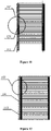
- the coating, for each of the cell pieces, the conductive adhesive material on the busbar located at the edge of the cell piece includes: coating the conductive adhesive material on the first busbar or the second busbar of the cell piece.
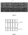
- a cell sheet having a predetermined thickness is provided, and the cell sheet is cut along a direction parallel to busbars of the cell sheet, to obtain cutting lines on a surface of the cell sheet.
- an entire cell sheet with a preset thickness may be provided.
- the surface of the cell sheet is printed with a metal pattern.
- the metal pattern serves as wires for conduction.
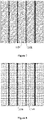
- the metal pattern includes busbars and fingers.
- the busbars are printed on both a first surface and a second surface of the cell sheet, and are used to conduct a current generated inside a cell to the outside.
- the number of busbars printed on the first surface of the cell sheet is equal to the number of busbars printed on the second surface of the cell sheet.
- the fingers are printed on the first surface and/or the second surface, and are used to collect an internal current.
- the EL test and the PL test may also help timely find and exclude the cell pieces with defects such as cracks, so as to avoid using such cell pieces in fabricating a photovoltaic module, thereby improving performance of the fabricated photovoltaic module.
Landscapes
- Photovoltaic Devices (AREA)
Applications Claiming Priority (2)
| Application Number | Priority Date | Filing Date | Title |
|---|---|---|---|
| CN201910711983.2A CN110379891B (zh) | 2019-08-02 | 2019-08-02 | 一种光伏组件的制备方法 |
| PCT/CN2019/128528 WO2021022771A1 (zh) | 2019-08-02 | 2019-12-26 | 一种光伏组件的制备方法 |
Publications (2)
| Publication Number | Publication Date |
|---|---|
| EP4009385A1 true EP4009385A1 (de) | 2022-06-08 |
| EP4009385A4 EP4009385A4 (de) | 2023-04-26 |
Family
ID=68257747
Family Applications (1)
| Application Number | Title | Priority Date | Filing Date |
|---|---|---|---|
| EP19940213.2A Pending EP4009385A4 (de) | 2019-08-02 | 2019-12-26 | Verfahren zur herstellung einer photovoltaischen anordnung |
Country Status (6)
| Country | Link |
|---|---|
| US (1) | US20220271189A1 (de) |
| EP (1) | EP4009385A4 (de) |
| JP (2) | JP7418548B2 (de) |
| CN (1) | CN110379891B (de) |
| AU (2) | AU2019460092B2 (de) |
| WO (1) | WO2021022771A1 (de) |
Families Citing this family (4)
| Publication number | Priority date | Publication date | Assignee | Title |
|---|---|---|---|---|
| CN110379891B (zh) * | 2019-08-02 | 2021-03-30 | 浙江晶科能源有限公司 | 一种光伏组件的制备方法 |
| US12094991B2 (en) | 2019-11-13 | 2024-09-17 | Maxeon Solar Pte. Ltd. | Hybrid dense solar cells and interconnects for solar modules and related methods of manufacture |
| CN111129220A (zh) * | 2019-12-24 | 2020-05-08 | 江苏爱康科技股份有限公司 | 一种叠瓦组件的制备方法 |
| CN115302120A (zh) * | 2022-09-16 | 2022-11-08 | 常州时创能源股份有限公司 | 电池片与光伏预制件的焊接方法 |
Family Cites Families (20)
| Publication number | Priority date | Publication date | Assignee | Title |
|---|---|---|---|---|
| US20140124014A1 (en) * | 2012-11-08 | 2014-05-08 | Cogenra Solar, Inc. | High efficiency configuration for solar cell string |
| WO2015152020A1 (ja) * | 2014-03-31 | 2015-10-08 | 株式会社カネカ | 太陽電池モジュールおよびその製造方法 |
| US11482639B2 (en) * | 2014-05-27 | 2022-10-25 | Sunpower Corporation | Shingled solar cell module |
| MY204717A (en) * | 2014-05-27 | 2024-09-10 | Maxeon Solar Pte Ltd | Shingled solar cell module |
| US9899546B2 (en) * | 2014-12-05 | 2018-02-20 | Tesla, Inc. | Photovoltaic cells with electrodes adapted to house conductive paste |
| US20160158890A1 (en) * | 2014-12-05 | 2016-06-09 | Solarcity Corporation | Systems and methods for scribing photovoltaic structures |
| US9590132B2 (en) * | 2014-12-05 | 2017-03-07 | Solarcity Corporation | Systems and methods for cascading photovoltaic structures |
| JP6411259B2 (ja) * | 2015-03-19 | 2018-10-24 | 国立研究開発法人産業技術総合研究所 | 太陽電池の製造方法 |
| CN205303477U (zh) * | 2015-05-22 | 2016-06-08 | 苏州沃特维自动化系统有限公司 | 太阳能电池片、太阳能电池组件及其电池片单元 |
| US20170194516A1 (en) * | 2015-12-30 | 2017-07-06 | Solarcity Corporation | Advanced design of metallic grid in photovoltaic structures |
| US20190019909A1 (en) * | 2015-12-30 | 2019-01-17 | Corner Star Limited | Advanced interconnect method for photovoltaic strings and modules |
| CN105489688A (zh) * | 2016-01-04 | 2016-04-13 | 协鑫集成科技股份有限公司 | 太阳能电池组件及其制备方法 |
| CN205911318U (zh) * | 2016-07-29 | 2017-01-25 | 无锡嘉瑞光伏有限公司 | 一种采用叠片设计的太阳能电池组件 |
| CN206672944U (zh) * | 2017-03-30 | 2017-11-24 | 隆基乐叶光伏科技有限公司 | 中心汇聚栅线电极、太阳能叠片电池及叠片组件 |
| KR102459719B1 (ko) * | 2017-06-14 | 2022-10-27 | 상라오 징코 솔라 테크놀러지 디벨롭먼트 컴퍼니, 리미티드 | 태양 전지, 태양전지 모듈과 그 제조 방법 |
| CN207265067U (zh) * | 2017-08-07 | 2018-04-20 | 阿特斯阳光电力集团有限公司 | 太阳能电池组件 |
| WO2019140605A1 (en) * | 2018-01-18 | 2019-07-25 | Flex, Ltd. | Busbar-less shingled array solar cells and methods of manufacturing solar modules |
| CN108899387B (zh) * | 2018-07-03 | 2021-06-18 | 彭延岩 | 一种能够即时在线转化成胶膜的导电胶和太阳能电池片的连接方法 |
| CN108922929B (zh) * | 2018-08-03 | 2024-07-02 | 浙江爱旭太阳能科技有限公司 | 贯孔双面叠瓦太阳能电池组件及制备方法 |
| CN110379891B (zh) * | 2019-08-02 | 2021-03-30 | 浙江晶科能源有限公司 | 一种光伏组件的制备方法 |
-
2019
- 2019-08-02 CN CN201910711983.2A patent/CN110379891B/zh active Active
- 2019-12-26 US US17/630,913 patent/US20220271189A1/en not_active Abandoned
- 2019-12-26 EP EP19940213.2A patent/EP4009385A4/de active Pending
- 2019-12-26 WO PCT/CN2019/128528 patent/WO2021022771A1/zh not_active Ceased
- 2019-12-26 AU AU2019460092A patent/AU2019460092B2/en active Active
- 2019-12-26 JP JP2022506190A patent/JP7418548B2/ja active Active
-
2023
- 2023-09-12 AU AU2023229510A patent/AU2023229510B2/en active Active
- 2023-10-16 JP JP2023177966A patent/JP2023176022A/ja active Pending
Also Published As
| Publication number | Publication date |
|---|---|
| JP2023176022A (ja) | 2023-12-12 |
| EP4009385A4 (de) | 2023-04-26 |
| JP7418548B2 (ja) | 2024-01-19 |
| AU2019460092A1 (en) | 2022-03-24 |
| CN110379891B (zh) | 2021-03-30 |
| AU2023229510A1 (en) | 2023-09-28 |
| JP2022542516A (ja) | 2022-10-04 |
| US20220271189A1 (en) | 2022-08-25 |
| CN110379891A (zh) | 2019-10-25 |
| AU2023229510B2 (en) | 2025-08-21 |
| WO2021022771A1 (zh) | 2021-02-11 |
| AU2019460092B2 (en) | 2023-08-10 |
Similar Documents
| Publication | Publication Date | Title |
|---|---|---|
| AU2023229510A1 (en) | Fabrication method for photovoltaic module and photovoltaic module | |
| CN110379867B (zh) | 硅基异质结太阳电池叠瓦光伏组件及其制备方法 | |
| EP3573111A1 (de) | Monokristalline solarzellen mit schindelanordnung und verfahren zur herstellung von solarmodulen damit | |
| CN216958062U (zh) | 背接触太阳能电池串、电池组件及光伏系统 | |
| CN114649443A (zh) | 背接触太阳能电池串及其制备方法、电池组件及光伏系统 | |
| CN106876503B (zh) | 采用中心汇聚栅线电极的太阳能叠片组件 | |
| CN108428751B (zh) | 一种叠瓦组件结构 | |
| EP3608975A1 (de) | Verfahren zur herstellung eines schindelsolarmoduls | |
| CN111477702A (zh) | 背接触太阳能电池组件及其制备方法 | |
| KR20200101832A (ko) | 버스 바가 없는 슁글드 어레이 태양 전지 및 태양광 모듈을 제조하는 방법 | |
| CN116031321A (zh) | 电池片、电池片的印刷方法及光伏组件 | |
| CN217405442U (zh) | 背接触电池的电极结构及具有其的背接触电池、光伏组件 | |
| CN108598199A (zh) | 一种背接触式分片太阳电池组件及制备方法 | |
| CN112271225A (zh) | 太阳能电池组件及其制造方法 | |
| CN119545949A (zh) | 光伏组件分步封装制造方法 | |
| US20220278243A1 (en) | Solar cell string, solar cell module, solar cell sheet and manufacturing method therefor | |
| CN114464704A (zh) | 一种叠瓦组件生产工艺 | |
| CN111129220A (zh) | 一种叠瓦组件的制备方法 | |
| CN108878577A (zh) | 一种柔性光伏组件制造方法 | |
| CN213184314U (zh) | 太阳能电池组件 | |
| CN109962121A (zh) | 一种抗热斑柔性晶硅组件及制备方法 | |
| CN212161825U (zh) | 背接触太阳能电池组件 | |
| CN110085697B (zh) | 一种低功率太阳能光伏组件加工方法 | |
| CN101350375A (zh) | 薄膜太阳电池模块及其加工方法 | |
| HK40068574A (en) | Fabrication method for photovoltaic assembly |
Legal Events
| Date | Code | Title | Description |
|---|---|---|---|
| STAA | Information on the status of an ep patent application or granted ep patent |
Free format text: STATUS: THE INTERNATIONAL PUBLICATION HAS BEEN MADE |
|
| PUAI | Public reference made under article 153(3) epc to a published international application that has entered the european phase |
Free format text: ORIGINAL CODE: 0009012 |
|
| STAA | Information on the status of an ep patent application or granted ep patent |
Free format text: STATUS: REQUEST FOR EXAMINATION WAS MADE |
|
| 17P | Request for examination filed |
Effective date: 20220301 |
|
| AK | Designated contracting states |
Kind code of ref document: A1 Designated state(s): AL AT BE BG CH CY CZ DE DK EE ES FI FR GB GR HR HU IE IS IT LI LT LU LV MC MK MT NL NO PL PT RO RS SE SI SK SM TR |
|
| REG | Reference to a national code |
Ref country code: HK Ref legal event code: DE Ref document number: 40068574 Country of ref document: HK |
|
| REG | Reference to a national code |
Ref country code: DE Ref legal event code: R079 Free format text: PREVIOUS MAIN CLASS: H01L0031180000 Ipc: H01L0031050000 |
|
| A4 | Supplementary search report drawn up and despatched |
Effective date: 20230324 |
|
| RIC1 | Information provided on ipc code assigned before grant |
Ipc: H02S 50/15 20140101ALI20230320BHEP Ipc: H02S 50/10 20140101ALI20230320BHEP Ipc: H01L 21/67 20060101ALI20230320BHEP Ipc: H01L 31/18 20060101ALI20230320BHEP Ipc: H01L 31/042 20140101ALI20230320BHEP Ipc: H01L 31/048 20140101ALI20230320BHEP Ipc: H01L 31/0224 20060101ALI20230320BHEP Ipc: H01L 31/05 20140101AFI20230320BHEP |
|
| STAA | Information on the status of an ep patent application or granted ep patent |
Free format text: STATUS: EXAMINATION IS IN PROGRESS |
|
| 17Q | First examination report despatched |
Effective date: 20260511 |