EP4009395A2 - Batterie tout solide - Google Patents
Batterie tout solide Download PDFInfo
- Publication number
- EP4009395A2 EP4009395A2 EP21210821.1A EP21210821A EP4009395A2 EP 4009395 A2 EP4009395 A2 EP 4009395A2 EP 21210821 A EP21210821 A EP 21210821A EP 4009395 A2 EP4009395 A2 EP 4009395A2
- Authority
- EP
- European Patent Office
- Prior art keywords
- active material
- anode
- material layer
- opposing region
- solid state
- Prior art date
- Legal status (The legal status is an assumption and is not a legal conclusion. Google has not performed a legal analysis and makes no representation as to the accuracy of the status listed.)
- Granted
Links
Images



Classifications
-
- H—ELECTRICITY
- H01—ELECTRIC ELEMENTS
- H01M—PROCESSES OR MEANS, e.g. BATTERIES, FOR THE DIRECT CONVERSION OF CHEMICAL ENERGY INTO ELECTRICAL ENERGY
- H01M4/00—Electrodes
- H01M4/02—Electrodes composed of, or comprising, active material
- H01M4/13—Electrodes for accumulators with non-aqueous electrolyte, e.g. for lithium-accumulators; Processes of manufacture thereof
- H01M4/134—Electrodes based on metals, Si or alloys
-
- H—ELECTRICITY
- H01—ELECTRIC ELEMENTS
- H01M—PROCESSES OR MEANS, e.g. BATTERIES, FOR THE DIRECT CONVERSION OF CHEMICAL ENERGY INTO ELECTRICAL ENERGY
- H01M4/00—Electrodes
- H01M4/02—Electrodes composed of, or comprising, active material
- H01M4/36—Selection of substances as active materials, active masses, active liquids
- H01M4/362—Composites
- H01M4/366—Composites as layered products
-
- H—ELECTRICITY
- H01—ELECTRIC ELEMENTS
- H01M—PROCESSES OR MEANS, e.g. BATTERIES, FOR THE DIRECT CONVERSION OF CHEMICAL ENERGY INTO ELECTRICAL ENERGY
- H01M4/00—Electrodes
- H01M4/02—Electrodes composed of, or comprising, active material
- H01M4/04—Processes of manufacture in general
- H01M4/0402—Methods of deposition of the material
- H01M4/0404—Methods of deposition of the material by coating on electrode collectors
-
- H—ELECTRICITY
- H01—ELECTRIC ELEMENTS
- H01M—PROCESSES OR MEANS, e.g. BATTERIES, FOR THE DIRECT CONVERSION OF CHEMICAL ENERGY INTO ELECTRICAL ENERGY
- H01M10/00—Secondary cells; Manufacture thereof
- H01M10/05—Accumulators with non-aqueous electrolyte
- H01M10/058—Construction or manufacture
- H01M10/0585—Construction or manufacture of accumulators having only flat construction elements, i.e. flat positive electrodes, flat negative electrodes and flat separators
-
- H—ELECTRICITY
- H01—ELECTRIC ELEMENTS
- H01M—PROCESSES OR MEANS, e.g. BATTERIES, FOR THE DIRECT CONVERSION OF CHEMICAL ENERGY INTO ELECTRICAL ENERGY
- H01M10/00—Secondary cells; Manufacture thereof
- H01M10/05—Accumulators with non-aqueous electrolyte
- H01M10/052—Li-accumulators
- H01M10/0525—Rocking-chair batteries, i.e. batteries with lithium insertion or intercalation in both electrodes; Lithium-ion batteries
-
- H—ELECTRICITY
- H01—ELECTRIC ELEMENTS
- H01M—PROCESSES OR MEANS, e.g. BATTERIES, FOR THE DIRECT CONVERSION OF CHEMICAL ENERGY INTO ELECTRICAL ENERGY
- H01M10/00—Secondary cells; Manufacture thereof
- H01M10/05—Accumulators with non-aqueous electrolyte
- H01M10/056—Accumulators with non-aqueous electrolyte characterised by the materials used as electrolytes, e.g. mixed inorganic/organic electrolytes
- H01M10/0561—Accumulators with non-aqueous electrolyte characterised by the materials used as electrolytes, e.g. mixed inorganic/organic electrolytes the electrolyte being constituted of inorganic materials only
- H01M10/0562—Solid materials
-
- H—ELECTRICITY
- H01—ELECTRIC ELEMENTS
- H01M—PROCESSES OR MEANS, e.g. BATTERIES, FOR THE DIRECT CONVERSION OF CHEMICAL ENERGY INTO ELECTRICAL ENERGY
- H01M10/00—Secondary cells; Manufacture thereof
- H01M10/42—Methods or arrangements for servicing or maintenance of secondary cells or secondary half-cells
- H01M10/4235—Safety or regulating additives or arrangements in electrodes, separators or electrolyte
-
- H—ELECTRICITY
- H01—ELECTRIC ELEMENTS
- H01M—PROCESSES OR MEANS, e.g. BATTERIES, FOR THE DIRECT CONVERSION OF CHEMICAL ENERGY INTO ELECTRICAL ENERGY
- H01M4/00—Electrodes
- H01M4/02—Electrodes composed of, or comprising, active material
- H01M4/13—Electrodes for accumulators with non-aqueous electrolyte, e.g. for lithium-accumulators; Processes of manufacture thereof
- H01M4/131—Electrodes based on mixed oxides or hydroxides, or on mixtures of oxides or hydroxides, e.g. LiCoOx
-
- H—ELECTRICITY
- H01—ELECTRIC ELEMENTS
- H01M—PROCESSES OR MEANS, e.g. BATTERIES, FOR THE DIRECT CONVERSION OF CHEMICAL ENERGY INTO ELECTRICAL ENERGY
- H01M4/00—Electrodes
- H01M4/02—Electrodes composed of, or comprising, active material
- H01M4/13—Electrodes for accumulators with non-aqueous electrolyte, e.g. for lithium-accumulators; Processes of manufacture thereof
- H01M4/139—Processes of manufacture
- H01M4/1391—Processes of manufacture of electrodes based on mixed oxides or hydroxides, or on mixtures of oxides or hydroxides, e.g. LiCoOx
-
- H—ELECTRICITY
- H01—ELECTRIC ELEMENTS
- H01M—PROCESSES OR MEANS, e.g. BATTERIES, FOR THE DIRECT CONVERSION OF CHEMICAL ENERGY INTO ELECTRICAL ENERGY
- H01M4/00—Electrodes
- H01M4/02—Electrodes composed of, or comprising, active material
- H01M4/36—Selection of substances as active materials, active masses, active liquids
- H01M4/38—Selection of substances as active materials, active masses, active liquids of elements or alloys
- H01M4/386—Silicon or alloys based on silicon
-
- H—ELECTRICITY
- H01—ELECTRIC ELEMENTS
- H01M—PROCESSES OR MEANS, e.g. BATTERIES, FOR THE DIRECT CONVERSION OF CHEMICAL ENERGY INTO ELECTRICAL ENERGY
- H01M4/00—Electrodes
- H01M4/02—Electrodes composed of, or comprising, active material
- H01M4/62—Selection of inactive substances as ingredients for active masses, e.g. binders, fillers
-
- H—ELECTRICITY
- H01—ELECTRIC ELEMENTS
- H01M—PROCESSES OR MEANS, e.g. BATTERIES, FOR THE DIRECT CONVERSION OF CHEMICAL ENERGY INTO ELECTRICAL ENERGY
- H01M4/00—Electrodes
- H01M4/02—Electrodes composed of, or comprising, active material
- H01M4/64—Carriers or collectors
- H01M4/66—Selection of materials
- H01M4/661—Metal or alloys, e.g. alloy coatings
-
- H—ELECTRICITY
- H01—ELECTRIC ELEMENTS
- H01M—PROCESSES OR MEANS, e.g. BATTERIES, FOR THE DIRECT CONVERSION OF CHEMICAL ENERGY INTO ELECTRICAL ENERGY
- H01M4/00—Electrodes
- H01M4/02—Electrodes composed of, or comprising, active material
- H01M4/64—Carriers or collectors
- H01M4/66—Selection of materials
- H01M4/665—Composites
- H01M4/667—Composites in the form of layers, e.g. coatings
-
- H—ELECTRICITY
- H01—ELECTRIC ELEMENTS
- H01M—PROCESSES OR MEANS, e.g. BATTERIES, FOR THE DIRECT CONVERSION OF CHEMICAL ENERGY INTO ELECTRICAL ENERGY
- H01M10/00—Secondary cells; Manufacture thereof
- H01M10/05—Accumulators with non-aqueous electrolyte
- H01M10/052—Li-accumulators
-
- H—ELECTRICITY
- H01—ELECTRIC ELEMENTS
- H01M—PROCESSES OR MEANS, e.g. BATTERIES, FOR THE DIRECT CONVERSION OF CHEMICAL ENERGY INTO ELECTRICAL ENERGY
- H01M4/00—Electrodes
- H01M4/02—Electrodes composed of, or comprising, active material
- H01M2004/026—Electrodes composed of, or comprising, active material characterised by the polarity
- H01M2004/027—Negative electrodes
-
- H—ELECTRICITY
- H01—ELECTRIC ELEMENTS
- H01M—PROCESSES OR MEANS, e.g. BATTERIES, FOR THE DIRECT CONVERSION OF CHEMICAL ENERGY INTO ELECTRICAL ENERGY
- H01M2220/00—Batteries for particular applications
- H01M2220/20—Batteries in motive systems, e.g. vehicle, ship, plane
-
- H—ELECTRICITY
- H01—ELECTRIC ELEMENTS
- H01M—PROCESSES OR MEANS, e.g. BATTERIES, FOR THE DIRECT CONVERSION OF CHEMICAL ENERGY INTO ELECTRICAL ENERGY
- H01M2300/00—Electrolytes
- H01M2300/0017—Non-aqueous electrolytes
- H01M2300/0065—Solid electrolytes
-
- H—ELECTRICITY
- H01—ELECTRIC ELEMENTS
- H01M—PROCESSES OR MEANS, e.g. BATTERIES, FOR THE DIRECT CONVERSION OF CHEMICAL ENERGY INTO ELECTRICAL ENERGY
- H01M2300/00—Electrolytes
- H01M2300/0017—Non-aqueous electrolytes
- H01M2300/0065—Solid electrolytes
- H01M2300/0068—Solid electrolytes inorganic
-
- Y—GENERAL TAGGING OF NEW TECHNOLOGICAL DEVELOPMENTS; GENERAL TAGGING OF CROSS-SECTIONAL TECHNOLOGIES SPANNING OVER SEVERAL SECTIONS OF THE IPC; TECHNICAL SUBJECTS COVERED BY FORMER USPC CROSS-REFERENCE ART COLLECTIONS [XRACs] AND DIGESTS
- Y02—TECHNOLOGIES OR APPLICATIONS FOR MITIGATION OR ADAPTATION AGAINST CLIMATE CHANGE
- Y02E—REDUCTION OF GREENHOUSE GAS [GHG] EMISSIONS, RELATED TO ENERGY GENERATION, TRANSMISSION OR DISTRIBUTION
- Y02E60/00—Enabling technologies; Technologies with a potential or indirect contribution to GHG emissions mitigation
- Y02E60/10—Energy storage using batteries
-
- Y—GENERAL TAGGING OF NEW TECHNOLOGICAL DEVELOPMENTS; GENERAL TAGGING OF CROSS-SECTIONAL TECHNOLOGIES SPANNING OVER SEVERAL SECTIONS OF THE IPC; TECHNICAL SUBJECTS COVERED BY FORMER USPC CROSS-REFERENCE ART COLLECTIONS [XRACs] AND DIGESTS
- Y02—TECHNOLOGIES OR APPLICATIONS FOR MITIGATION OR ADAPTATION AGAINST CLIMATE CHANGE
- Y02P—CLIMATE CHANGE MITIGATION TECHNOLOGIES IN THE PRODUCTION OR PROCESSING OF GOODS
- Y02P70/00—Climate change mitigation technologies in the production process for final industrial or consumer products
- Y02P70/50—Manufacturing or production processes characterised by the final manufactured product
Definitions
- the present disclosure relates to an all solid state battery.
- An all solid state battery is a battery including a solid electrolyte layer between a cathode active material layer and an anode active material layer, and has advantages in that it is easy to simplify a safety device as compared with a liquid battery including a liquid electrolyte containing flammable organic solvents.
- Patent Literature 1 discloses a method for producing a sulfide solid battery, the method comprising a step of obtaining a predoped material by doping a black lead or a lithium titanate with lithium; a step of obtaining an anode mixture by mixing a sulfide solid electrolyte, a silicon based active material, and the predoped material; a step of obtaining an anode by stacking the anode mixture on the surface of a cathode current collector including copper.
- Patent Literature 1 Japanese Patent Application Laid-Open ( JP-A) No. 2019-106352
- the sulfide solid electrolyte included in the anode active material layer and the anode current collector react with each other to generate a metal sulfide (such as CuS) having high electron conductivity.
- the metal sulfide may be a cause of a minute short circuit (voltage drop), by being diffused.
- the size of the anode in plan view is made larger than the size of the cathode in some cases.
- the occurrence of a short circuit due to the contact between the cathode and the anode, during the production of the all solid state battery may be suppressed.
- the size of the anode relatively large, the occurrence points of Li dendrite may be scattered.
- the charge/discharge reaction in the anode active material layer tends to be uneven.
- a region where the anode active material layer and the cathode active material layer are opposing to each other is regarded as an opposing region; and a region where the anode active material layer and the cathode active material layer are not opposing to each other is regarded as a non-opposing region.
- the opposing region since the ion conductive distance and the electron conductive distance in the anode active material layer are the shortest, the potential of the anode active material tends to be decrease by charging.
- the potential of the anode active material is hardly decreased by charging. Therefore, in the anode active material layer located in the non-opposing region, the minute short circuit described above tends to occur.
- the present disclosure has been made in view of the above circumstances, and a main object of the present disclosure is to provide an all solid state battery wherein the occurrence of a minute short circuit, in an anode active material layer located in a non-opposing region, is suppressed.
- the present inventor has carried out extensive studies, and found out that, by being creative with a coat layer (a coat layer including lithium titanate) provided on a surface of an anode current collector, uniformity of a charge/discharge reaction in an anode active material layer may be improved.
- the lithium titanate included in the coat layer (particularly Li 4 Ti 5 O 12 ) has an electron conductivity in the charged state. However, it is insulated when Li is extracted at occurrence of an inner short circuit, for example. By placing the coat layer having such a shutdown function between the anode active material layer and the anode current collector, improvement in safety may be expected.
- the resistance itself increases.
- the resistance difference between the opposing region and the non-opposing region decreases, so that a charge reaction may be progressed (the potential of the anode active material may be decreased) in the anode active material layer located in the non-opposing region.
- the present disclosure provides an all solid state battery comprising a cathode including a cathode active material layer, and a cathode current collector; an anode including an anode active material layer, and an anode current collector; and a solid electrolyte layer placed between the cathode active material layer and the anode active material layer, and the anode active material layer includes an anode active material, and a sulfide solid electrolyte, the anode current collector is a current collector that react with the sulfide solid electrolyte at an open circuit potential of the anode active material, in a thickness direction, the all solid state battery includes an opposing region where the anode active material layer and the cathode active material layer are opposing to each other; and a non-opposing region where the anode active material layer and the cathode active material layer are not opposing to each other, the anode current collector includes a coating layer including a lithium titanate, on a surface of
- an all solid state battery wherein the occurrence of a minute short circuit, in an anode active material layer located in a non-opposing region, is suppressed, may be obtained.
- the anode active material may include Si.
- the anode current collector may include Cu or Ni.
- the coating layer may include the existence portion in an entire area of the opposing region.
- the coating layer may include the existence portion and the non-existence portion in the opposing region.
- the coating layer may include the non-existence portion in an entire area of the non-opposing region.
- the coating layer may include the existence portion and the non-existence portion in the non-opposing region.
- the non-existence portion in the non-opposing region may be placed along a longitudinal direction of the all solid state battery.
- the non-existence portion in the non-opposing region may be placed along a transverse direction of the all solid state battery.
- the non-existence portion in the non-opposing region may be placed so as to surround the cathode active material layer, continuously or discontinuously.
- the all solid state battery in the present disclosure exhibits effects that the occurrence of a minute short circuit in a non-opposing region may be suppressed.
- FIG. 1A is a schematic cross-sectional view illustrating an example of an all solid state battery in the present disclosure, and corresponds to an X-X cross-sectional view of FIG. 1B .
- All solid state battery 10 shown in FIGS. 1A and 1B comprises cathode C including cathode active material layer 1, and cathode current collector 2; anode A including anode active material layer 3, and anode current collector 4; and solid electrolyte layer 5 placed between cathode active material layer 1 and anode active material layer 3.
- Anode active material layer 3 includes an anode active material, and a sulfide solid electrolyte.
- anode current collector 4 is a current collector that react with the sulfide solid electrolyte at an open circuit potential of the anode active material.
- all solid state battery 10 includes opposing region R 1 where anode active material layer 3 and cathode active material layer 1 are opposing to each other; and non-opposing region R 2 where anode active material layer 3 and cathode active material layer 1 are not opposing to each other.
- anode current collector 4 includes coating layer 6 including a lithium titanate, on a surface of anode active material layer 3 side.
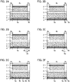
- coating layer 6 includes existence portion 6a and non-existence portion 6b, in the region R B specified by an outer edge of anode current collector 4. Further, in plan view, coating layer 6 includes existence portion 6a in at least a part of opposing region R 1 , and includes non-existence portion 6b in at least a part of non-opposing region R 2 .
- an all solid state battery wherein the occurrence of a minute short circuit, in an anode active material layer located in a non-opposing region, is suppressed, may be obtained.
- the size of the anode is made larger than the size of the cathode, a minute short circuit is likely to occur in the anode active material layer located in the non-opposing region.
- the coating layer in the opposing region while not placing the coating layer in the non-opposing region, focusing on the coating layer, the resistance difference between the opposing region and the non-opposing region is decreased, and as the result, a charge reaction may be progressed (the potential of the anode active material may be decreased) in the anode active material layer located in the non-opposing region.
- the anode in the present disclosure includes an anode active material layer, a coating layer, and an anode current collector. Also, as shown in FIGS. 1A and 1B , in plan view, anode active material layer 3 is larger than cathode active material layer 1. Particularly, in plan view, anode active material layer 3 is preferably placed so as to include the entire circumference of cathode active material layer 1. The reason therefor is to effectively suppress the short circuit due to the contact of anode active material layer 3 and cathode active material layer 1.
- the region where the anode active material layer and the cathode active material layer are opposing to each other is regarded as an opposing region; and the region where the anode active material layer and the cathode active material layer are not opposing to each other is regarded as a non-opposing region.
- An anode active material layer includes at least an anode active material and a sulfide solid electrolyte. Also, the anode active material layer may further include at least one of a conductive material, and a binder.
- the kind of the anode active material is not particularly limited, and examples thereof may include a metal active material, and a carbon active material.
- the metal active material may include an active material including a metal such as Si, Sn, Li, In, and Al.
- the metal active material may be a simple substance of the metal, may be an alloy of the metal, and may be an oxide of the metal.
- the metal active material including Si may include a Si simple substance, a Si alloy (such as an alloy including Si as a main component), and a Si oxide.
- examples of the carbon active material may include mesocarbon microbeads (MCMB), highly oriented pyrolytic graphite (HOPG), hard carbon, and soft carbon.
- the open circuit potential of the anode active material is, for example, 1.5 V (vs. Li/Li + ) or more, and may be 2.0 V (vs. Li/Li + ) or more. Meanwhile, the open circuit potential of the anode active material may be, for example, 3.2 V (vs. Li/Li + ) or less. In particular, the open circuit potential of the anode active material before the initial charge (at the time of battery assembly) may be in the above range. Also, the anode active material may be a material having an expansion rate, at the time of charging, larger than lithium titanate included in the coating layer to be described later.
- Examples of the shape of the anode active material may include a granular shape.
- the average particle size (D 50 ) of the anode active material is not particularly limited; and is, for example, 10 nm or more, and may be 100 nm or more. Meanwhile, the average particle size (D 50 ) of the anode active material is, for example, 50 ⁇ m or less, and may be 20 ⁇ m or less.
- the average particle size (D 50 ) may be calculated from the measurement by, for example, a laser diffraction particle size analyzer, and a scanning electron microscope (SEM).
- the proportion of the anode active material in the anode active material layer is, for example, 20 weight% or more and 80 weight% or less.
- the sulfide solid electrolyte may include a solid electrolyte containing a Li element, an X element (X is at least one kind of P, As, Sb, Si, Ge, Sn, B, Al, Ga, and In), and a S element. Also, the sulfide solid electrolyte may further include at least one of an O element and a halogen element. Examples of the halogen element may include a F element, a Cl element, a Br element, and an I element.
- the sulfide solid electrolyte may be a glass (amorphous), and may be a glass ceramic.
- Examples of the sulfide solid electrolyte may include Li 2 S-P 2 S 5 , LiI-Li 2 S-P 2 S 5 , LiI-LiBr-Li 2 S-P 2 S 5 , Li 2 S-SiS 2 , Li 2 S-GeS 2 , and Li 2 S-P 2 S 5 -GeS 2 .
- Examples of the shape of the sulfide solid electrolyte may include a granular shape.
- Examples of the conductive material may include a carbon material, a metal particle, and a conductive polymer.
- the carbon material may include particulate carbon materials such as acetylene black (AB) and Ketjen black (KB); and fibrous carbon materials such as carbon fiber, carbon nanotube (CNT), and carbon nanofiber (CNF).
- examples of the binder may include fluorine-based binders, polyimide-based binders, and rubber-based binders.
- the thickness of the anode active material layer is, for example, 0.1 ⁇ m or more and 1000 ⁇ m or less.
- the anode current collector is a current collector that react with the sulfide solid electrolyte at an open circuit potential of the anode active material.
- Examples of the anode current collector may include a metal current collector.
- Examples of the metal current collector may include a current collector including a metal such as Cu, and Ni.
- the metal current collector may be a simple substance of the metal, and may be an alloy of the metal.
- Examples of the shape of the anode current collector may include a foil shape. Also, in plan view, the anode current collector is preferably placed so as to include the entire circumference of the anode active material layer.
- the coating layer is a layer placed on a surface of the anode current collector on the side of the anode active material layer.
- the coating layer includes one or two or more of an existence portion and a non-existence portion respectively, in the region specified by an outer edge of the anode current collector.
- the number of the existence portions means the number of the existence portions formed continuously in plan view. The same applies to the number of the non-existence portions. For example, when a frame-shaped non-existence portion is placed around a rectangular existence portion, the number of existence portion and the number of non-existence portion are 1, respectively.
- the non-existence portion may be regarded as a defective portion.
- the anode active material layer and the anode current collector are usually in direct contact with each other.
- the coating layer is a layer including lithium titanate.
- the lithium titanate is a compound including Li, Ti, and O. Examples thereof may include Li 4 Ti 5 O 12 , Li 4 TiO 4 , Li 2 TiO 3 , and Li 2 Ti 3 O 7 .
- lithium titanate included in the coating layer may be doped with Li.
- the proportion of lithium titanate in the coating layer is, for example, 50 weight% or more, and may be 70 weight% or more, and may be 90 weight% or more.
- the coating layer may further include a binder.
- a binder By adding a binder, adhesiveness of the coating layer is improved, and adhesion of the anode active material layer and the anode current collector is improved.
- the coating layer may or may not include a sulfide solid electrolyte. Since the sulfide solid electrolyte and the binder are the same as those described above, description thereof is omitted here.
- the thickness of the coating layer is not particularly limited, and is, for example, 1 ⁇ m or more, and may be 2 ⁇ m or more. If the thickness of the coating layer is too thin, there is a possibility that a sufficient shutdown function may not be exhibited. Meanwhile, the thickness of the coating layer is, for example, 15 ⁇ m or less, and may be 10 ⁇ m or less. If the thickness of the coating layer is too thick, the thickness of the anode active material layer will be relatively small, and the volume energy density may be decreased.
- the thickness of the coating layer is smaller than the thickness of the anode active material layer.
- the reason therefor is to suppress the decrease in the volume energy density.
- the thickness of the coating layer with respect to the thickness of the anode active material layer is, for example, 3% or more, and may be 5% or more. Meanwhile, the thickness of the coating layer with respect to the thickness of the anode active material layer is, for example, 20% or less, and may be 13% or less.
- the method for forming the coating layer is not particularly limited, and examples thereof may include a method wherein a slurry is produced by dispersing lithium titanate in a dispersion medium, coating an anode current collector with the slurry, and drying the slurry.
- the coating layer in the present disclosure includes, in plan view, the existence portion in at least a part of the opposing region, and includes the non-existence portion in at least a part of the non-opposing region.
- coating layer 6 may include existence portion 6a in the entire area of opposing region R 1 .
- the shutdown function may be effectively exhibited.
- coating layer 6 in FIG. 2A includes non-existence portion 6b in the entire area of non-opposing region R 2 .
- non-existence portion 6b in the entire area of non-opposing region R 2 , the resistance difference between the opposing region and the non-opposing region may be reduced, and the uniformity of charge/discharge reaction in the anode active material layer may be further improved.
- coating layer 6 may include both of existence portion 6a and non-existence portion 6b in opposing region R 1 .
- non-existence portion 6b in opposing region R 1 , the resistance difference between the opposing region and the non-opposing region may further be decreased.
- W 1 is not particularly limited, and is, for example, 0.1 mm or more and 20 mm or less.
- the proportion of the area of existence portion 6a to the total area of existence portion 6a and non-existence portion 6b is, for example, 70% or more, may be 80% or more, and may be 90% or more.
- non-existence portion 6b in opposing region R 1 and non-existence portion 6b in non-opposing region R 2 may be continuously formed.
- coating layer 6 may include two or more existence portions 6a in opposing region R 1 .
- coating layer 6 may include two or more non-existence portions 6b in opposing region R 1 .
- coating layer 6 may include both of existence portion 6a and non-existence portion 6b in non-opposing region R 2 .
- the end portion of existence portion 6a in non-opposing region R 2 may coincide with the end portion of anode active material layer 3. Since the volume variation due to charge/discharge of the lithium titanate included in existence portion 6a (coating layer 6) is small, the damage of an exterior body may be suppressed by placing such existence portion 6a at the outermost side.
- existence portion 6a in opposing region R 1 and existence portion 6a in non-opposing region R 2 may be continuously formed. Thereby a cracking at the end portion of existence portion 6a due to the confining pressure may be suppressed.
- W 2 is not particularly limited, and is, for example, 0.1 mm or more and 10 mm or less.
- the proportion of the area of non-existence portion 6b to the total area of non-existence portion 6b and existence portion 6a is, for example, 70% or more, may be 80% or more, and may be 90% or more.
- the end portion of existence portion 6a in non-opposing region R 2 may coincide with the end portion of anode active material layer 3.
- coating layer 6 may include two or more existence portions 6a in non-opposing region R 2 .
- the coating layer may include two or more non-existence portions in the non-opposing region.
- non-existence portion 6b in non-opposing region may be placed along the longitudinal direction of the all solid state battery in plan view. In this case, two non-existence portions 6b are placed so as to face each other. However, non-existence portion 6b may be placed on either side. Also, as shown in FIG. 3B , non-existence portion 6b in the non-opposing region may be placed along the transverse direction of the all solid state battery in plan view. Also in this case, although two non-existence portions 6b are placed so as to face each other, non-existence portion 6b may be placed on either side. Also, as shown in FIG.
- non-existence portion 6b in the non-opposing region may be placed so as to surround the cathode active material layer (not shown in the figure), continuously in plan view.
- non-existence portion 6b in the non-opposing region may be placed so as to surround the cathode active material layer (not shown in the figure), discontinuously (intermittently) in plan view.
- the cathode in the present disclosure includes a cathode active material layer, and a cathode current collector.
- the cathode active material layer is a layer including at least a cathode active material.
- the cathode active material layer may include at least one of a sulfide solid electrolyte, a conductive material, and a binder, as necessary.
- the cathode active material may include an oxide active material.
- the oxide active material may include rock salt bed type active materials such as LiCoO 2 , LiMnO 2 , LiNiO 2 , LiVO 2 , LiNi 1/3 Co 1/3 Mn 1/3 O 2 ; spinel type active materials such as LiMn 2 O 4 , Li 4 Ti 5 O 12 , and Li(Ni 0.5 Mn 1.5 )O 4 ; and olivine type active materials such as LiFePO 4 , LiMnPO 4 , LiNiPO 4 , and LiCoPO 4 .
- a protecting layer including a Li ion conductive oxide may be formed on the surface of the oxide active material.
- the reason therefor is to suppress the reaction between the oxide active material and the sulfide solid electrolyte.
- the Li ion conductive oxide may include LiNbO 3 .
- the thickness of the protecting layer is, for example, 1 nm or more and 30 nm or less.
- Li 2 S may be used, for example, as the cathode active material.
- Examples of the shape of the cathode active material may include a granular shape.
- the average particle size (D 50 ) of the cathode active material is not particularly limited; and is, for example, 10 nm or more, and may be 100 nm or more. Meanwhile, the average particle size (D 50 ) of the cathode active material is, for example, 50 ⁇ m or less, and may be 20 ⁇ m or less.
- the sulfide solid electrolyte, the conductive material and the binder used for the cathode active material layer may be in the same contents as those described in "1. Anode" above; thus, the description herein is omitted.
- the thickness of the cathode active material layer is, for example, 0.1 ⁇ m or more and 1000 ⁇ m or less.
- examples of the materials for the cathode current collector may include SUS, aluminum, nickel, iron, titanium, and carbon.
- the solid electrolyte layer in the present disclosure is a layer placed between the cathode active material layer and the anode active material layer, and is a layer including at least a solid electrolyte.
- the solid electrolyte layer preferably includes a sulfide solid electrolyte as the solid electrolyte.
- the solid electrolyte layer may include a binder.
- the sulfide solid electrolyte, and the binder used for the solid electrolyte layer may be in the same contents as those described in "1. Anode” above; thus, the description herein is omitted.
- the thickness of the solid electrolyte layer is, for example, 0.1 ⁇ m or more and 1000 ⁇ m or less.
- the all solid state battery in the present disclosure includes at least one power generation unit including a cathode active material layer, a solid electrolyte layer, and an anode active material layer, and may include two or more of them.
- the all solid state battery includes a plurality of the power generation units, they may be connected in parallel, and may be connected in series.
- All solid state battery 10 shown in FIG. 4 includes power generation unit A and power generation unit B, and these are connected in parallel. Specifically, in all solid state battery 10, based on anode current collector 4, first coating layer 6x, first anode active material layer 3a, first solid electrolyte layer 5a, first cathode active material layer 1a, and first cathode current collector 2a are placed in this order, on one surface s11; and second coating layer 6y, second anode active material layer 3b, second solid electrolyte layer 5b, second cathode active material layer 1b, and second cathode current collector 2b are placed in this order, on the other surface s12.
- all solid state battery 10 includes cathode tab 2t to which first cathode current collector 2a and second cathode current collector 2b are connected; and anode tab 4t located at an end of anode current collector 4. Also, the insulating layer 7 is placed on the side surface of power generation unit A and power generation unit B. Such all solid state battery 10 has an advantage that the stress due to the difference in the stretching ability of the cathode layer and the anode layer is less likely to occur, since the configuration of the other layers is symmetrical with respect to anode current collector 4.
- the all solid state battery in the present disclosure is provided with an exterior body that houses a cathode, a solid electrolyte layer, and an anode.
- the kind of the exterior body is not particularly limited; and examples thereof may include a laminate exterior body.
- the all solid state battery in the present disclosure may include a confining jig that applies a confining pressure along the thickness direction, to the cathode, the solid electrolyte layer and the anode.
- a confining pressure By applying the confining pressure, a favorable ion conductive path and an electron conductive path may be formed.
- the confining pressure is, for example, 0.1 MPa or more, may be 1 MPa or more, and may be 5 MPa or more. Meanwhile, the confining pressure is, for example, 100 MPa or less, may be 50 MPa or less, and may be 20 MPa or less.
- the all solid state battery in the present disclosure is typically an all solid state lithium ion secondary battery.
- the use of all solid state battery is not particularly limited, and examples thereof may include a power supply of a vehicle such as a hybrid electric vehicle, a battery electric vehicle, a gasoline-powered vehicle, and a diesel-powered vehicle. In particular, it is preferably used in the driving power supply of a hybrid electric vehicle, or a battery electric vehicle.
- the all solid state battery in the present disclosure may be used as a power source for moving objects other than vehicles, such as railroad vehicles, ships, and airplanes, or may be used as a power source for electric appliances such as information processing apparatuses.
- the present disclosure is not limited to the embodiments.
- the embodiments are exemplification, and any other variations are intended to be included in the technical scope of the present disclosure if they have substantially the same constitution as the technical idea described in the claim of the present disclosure and offer similar operation and effect thereto.
- a slurry including the followings were prepared: a lithium titanate (Li 4 Ti 5 O 12 particles, average particle size of 0.7 ⁇ m), a sulfide solid electrolyte (10LiI-15LiBr-75(0.75Li 2 S-0.25P 2 S 5 )), a binder (styrenebutadiene rubber, SBR) and a dispersing medium.
- a coating layer thickness of 5 ⁇ m was formed by coating an anode current collector (a Ni foil, thickness of 15 ⁇ m) with this slurry, and drying.
- an anode slurry including the followings were prepared: an anode active material (Si particles, average particle size of 2.5 ⁇ m), a sulfide solid electrolyte (10LiI-15LiBr-75(0.75Li 2 S-0.25P 2 S 5 )), a conductive material (VGCF), a binder (SBR) and a dispersing medium.
- An anode active material layer (thickness of 50 ⁇ m) was formed by coating the coating layer with the obtained anode slurry, and drying. Thereby, an anode including an anode current collector, a coating layer, and an anode active material layer was obtained.
- a cathode slurry including the followings were prepared: a cathode active material (LiNi 1/3 Co 1/3 Mn 1/3 O 2 coated with LiNbO 3 ), a sulfide solid electrolyte (10LiI-15LiBr-75(0.75Li 2 S-0.25P 2 S 5 )), a conductive material (VGCF), a binder (PVDF) and a dispersing medium.
- a cathode active material layer (thickness of 60 ⁇ m) was formed by coating a cathode current collector (an Al foil, thickness of 15 ⁇ m) with the obtained cathode slurry, and drying. Thereby, a cathode including a cathode current collector, and a cathode active material layer was obtained.
- a solid electrolyte layer (thickness of 30 ⁇ m) was obtained by charging a sulfide solid electrolyte (10LiI-15LiBr-75(0.75Li 2 S-0.25P 2 S 5 )) into a ceramic tube with an inner cross-sectional area of 1 cm 2 , and pressing under 4 ton/cm 2 .
- An evaluation cell was obtained by placing the cathode on one surface of the solid electrolyte layer, placing the anode on another surface of the solid electrolyte layer, and pressing.
- the width of anode current collector 4, coating layer 6, anode active material layer 3, and solid electrolyte layer 5 was 13 mm respectively
- the width of cathode active material layer 1 was 11 mm
- the width of cathode current collector 2 was 10 mm.
- An evaluation cell was obtained in the same manner as in Comparative Example 1 except that the width of coating layer 6 was changed to 11 mm, as shown in FIG. 5B .
- An evaluation cell was obtained in the same manner as in Comparative Example 1 except that the width of coating layer 6 was changed to 10 mm, as shown in FIG. 5C .
- An evaluation cell was obtained in the same manner as in Comparative Example 1 except that the shape in plan view of coating layer 6 was changed, as shown in FIG. 5D .
Landscapes
- Chemical & Material Sciences (AREA)
- Chemical Kinetics & Catalysis (AREA)
- Electrochemistry (AREA)
- General Chemical & Material Sciences (AREA)
- Engineering & Computer Science (AREA)
- Materials Engineering (AREA)
- Manufacturing & Machinery (AREA)
- Composite Materials (AREA)
- Physics & Mathematics (AREA)
- Condensed Matter Physics & Semiconductors (AREA)
- General Physics & Mathematics (AREA)
- Inorganic Chemistry (AREA)
- Secondary Cells (AREA)
- Battery Electrode And Active Subsutance (AREA)
- Cell Electrode Carriers And Collectors (AREA)
Applications Claiming Priority (1)
| Application Number | Priority Date | Filing Date | Title |
|---|---|---|---|
| JP2020201092A JP7484683B2 (ja) | 2020-12-03 | 2020-12-03 | 全固体電池 |
Publications (3)
| Publication Number | Publication Date |
|---|---|
| EP4009395A2 true EP4009395A2 (fr) | 2022-06-08 |
| EP4009395A3 EP4009395A3 (fr) | 2022-06-22 |
| EP4009395B1 EP4009395B1 (fr) | 2023-10-18 |
Family
ID=78806383
Family Applications (1)
| Application Number | Title | Priority Date | Filing Date |
|---|---|---|---|
| EP21210821.1A Active EP4009395B1 (fr) | 2020-12-03 | 2021-11-26 | Batterie tout solide |
Country Status (5)
| Country | Link |
|---|---|
| US (2) | US11984585B2 (fr) |
| EP (1) | EP4009395B1 (fr) |
| JP (1) | JP7484683B2 (fr) |
| KR (1) | KR102698856B1 (fr) |
| CN (1) | CN114613940B (fr) |
Families Citing this family (5)
| Publication number | Priority date | Publication date | Assignee | Title |
|---|---|---|---|---|
| CN116565156A (zh) * | 2022-01-28 | 2023-08-08 | 通用汽车环球科技运作有限责任公司 | 用于高性能电池组的电活性材料 |
| CN115579454B (zh) * | 2022-11-07 | 2024-07-23 | 哈尔滨工业大学 | 一种硫化物固态电解质复合固态正极及固态电池 |
| KR20250010311A (ko) * | 2023-07-12 | 2025-01-21 | 주식회사 엘지에너지솔루션 | 리튬 이차 전지용 음극, 리튬 이차 전지용 음극의 제조 방법 및 음극을 포함하는 리튬 이차 전지 |
| KR20250115732A (ko) * | 2024-01-24 | 2025-07-31 | 삼성에스디아이 주식회사 | 전고체 이차전지 |
| KR20250146033A (ko) * | 2024-03-29 | 2025-10-13 | 삼성에스디아이 주식회사 | 전고체 전지용 음극 및 이를 포함하는 전고체 전지 |
Citations (1)
| Publication number | Priority date | Publication date | Assignee | Title |
|---|---|---|---|---|
| JP2019106352A (ja) | 2017-12-08 | 2019-06-27 | トヨタ自動車株式会社 | 硫化物固体電池の製造方法 |
Family Cites Families (22)
| Publication number | Priority date | Publication date | Assignee | Title |
|---|---|---|---|---|
| US8080334B2 (en) * | 2005-08-02 | 2011-12-20 | Panasonic Corporation | Lithium secondary battery |
| JP2011238568A (ja) * | 2010-05-13 | 2011-11-24 | Toyota Motor Corp | リチウムイオン二次電池及び二次電池システム |
| JP2012079522A (ja) * | 2010-09-30 | 2012-04-19 | Sumitomo Electric Ind Ltd | 非水電解質電池とその製造方法 |
| CN103548196B (zh) * | 2011-05-27 | 2016-03-02 | 丰田自动车株式会社 | 双极全固体电池 |
| JP2014199714A (ja) | 2011-08-09 | 2014-10-23 | パナソニック株式会社 | 非水電解質二次電池用負極およびその非水電解質二次電池 |
| JP2013243097A (ja) * | 2012-05-22 | 2013-12-05 | Toyota Motor Corp | 二次電池 |
| JP5742858B2 (ja) * | 2013-01-15 | 2015-07-01 | トヨタ自動車株式会社 | 全固体電池およびその製造方法 |
| WO2014141962A1 (fr) | 2013-03-11 | 2014-09-18 | 株式会社村田製作所 | Batterie à électrolyte complètement solide |
| JP2015011959A (ja) | 2013-07-02 | 2015-01-19 | 三菱マテリアル株式会社 | リチウムイオン二次電池 |
| JP6048396B2 (ja) * | 2013-12-26 | 2016-12-21 | トヨタ自動車株式会社 | 全固体電池の製造方法 |
| JP2016081881A (ja) | 2014-10-22 | 2016-05-16 | トヨタ自動車株式会社 | 非水電解液二次電池 |
| JP6319335B2 (ja) | 2016-01-18 | 2018-05-09 | トヨタ自動車株式会社 | 全固体電池の製造方法 |
| EP3496188B1 (fr) | 2017-12-08 | 2021-03-31 | Toyota Jidosha Kabushiki Kaisha | Procédé de fabrication de batterie à électrolyte solide au sulfure |
| JP6863299B2 (ja) * | 2018-01-09 | 2021-04-21 | トヨタ自動車株式会社 | 全固体電池 |
| DE112019001591B4 (de) * | 2018-03-28 | 2024-07-25 | Tdk Corporation | Festkörperbatterie |
| JP6973319B2 (ja) * | 2018-07-27 | 2021-11-24 | トヨタ自動車株式会社 | 固体電池用電極及び固体電池 |
| JP7420469B2 (ja) | 2018-09-25 | 2024-01-23 | トヨタ自動車株式会社 | 負極合材 |
| JP7172679B2 (ja) | 2019-02-06 | 2022-11-16 | トヨタ自動車株式会社 | 全固体電池 |
| JP7167752B2 (ja) | 2019-02-12 | 2022-11-09 | トヨタ自動車株式会社 | 全固体電池 |
| JP7314768B2 (ja) | 2019-03-22 | 2023-07-26 | トヨタ自動車株式会社 | 全固体電池の製造方法及び全固体電池 |
| JP2020174004A (ja) | 2019-04-12 | 2020-10-22 | 株式会社Soken | 全固体電池 |
| JP7211262B2 (ja) | 2019-05-20 | 2023-01-24 | トヨタ自動車株式会社 | 硫化物全固体電池の製造方法 |
-
2020
- 2020-12-03 JP JP2020201092A patent/JP7484683B2/ja active Active
-
2021
- 2021-11-24 US US17/535,190 patent/US11984585B2/en active Active
- 2021-11-24 KR KR1020210163334A patent/KR102698856B1/ko active Active
- 2021-11-25 CN CN202111411081.0A patent/CN114613940B/zh active Active
- 2021-11-26 EP EP21210821.1A patent/EP4009395B1/fr active Active
-
2024
- 2024-03-25 US US18/614,919 patent/US20240234703A1/en active Pending
Patent Citations (1)
| Publication number | Priority date | Publication date | Assignee | Title |
|---|---|---|---|---|
| JP2019106352A (ja) | 2017-12-08 | 2019-06-27 | トヨタ自動車株式会社 | 硫化物固体電池の製造方法 |
Also Published As
| Publication number | Publication date |
|---|---|
| US20240234703A1 (en) | 2024-07-11 |
| CN114613940A (zh) | 2022-06-10 |
| JP7484683B2 (ja) | 2024-05-16 |
| CN114613940B (zh) | 2023-08-04 |
| KR20220078485A (ko) | 2022-06-10 |
| EP4009395B1 (fr) | 2023-10-18 |
| KR102698856B1 (ko) | 2024-08-27 |
| US11984585B2 (en) | 2024-05-14 |
| JP2022088945A (ja) | 2022-06-15 |
| EP4009395A3 (fr) | 2022-06-22 |
| US20220181609A1 (en) | 2022-06-09 |
Similar Documents
| Publication | Publication Date | Title |
|---|---|---|
| EP4009395B1 (fr) | Batterie tout solide | |
| KR102104009B1 (ko) | 리튬 고체 전지 | |
| KR20170071408A (ko) | 전고체 전지 및 전고체 전지의 제조 방법 | |
| EP4027427B1 (fr) | Batterie tout solide | |
| KR20220069624A (ko) | 금속계 입자를 포함하는 코팅층이 구비된 전고체 전지용 음극 | |
| KR102860531B1 (ko) | 양극 및 이를 포함하는 이차전지 | |
| US12555773B2 (en) | All solid state battery | |
| US20220246913A1 (en) | Anode active materal layer | |
| US20220320512A1 (en) | All solid state battery | |
| JP2023009793A (ja) | 全固体電池 | |
| JP2022097800A (ja) | 全固体電池 | |
| US10319987B2 (en) | Active material with expansion structure for use in lithium ion batteries | |
| US12334545B2 (en) | All solid state battery | |
| US20240128430A1 (en) | Electrode body and battery | |
| US20250323314A1 (en) | Cathode layer and solid-state battery | |
| JP2022088979A (ja) | 全固体電池 | |
| JP2025101578A (ja) | 負極および電池 | |
| JP2022088978A (ja) | 全固体電池 | |
| KR20250035450A (ko) | 전고체 전지 및 전고체 전지의 제조 방법 | |
| JP2022088952A (ja) | 全固体電池 |
Legal Events
| Date | Code | Title | Description |
|---|---|---|---|
| PUAI | Public reference made under article 153(3) epc to a published international application that has entered the european phase |
Free format text: ORIGINAL CODE: 0009012 |
|
| STAA | Information on the status of an ep patent application or granted ep patent |
Free format text: STATUS: REQUEST FOR EXAMINATION WAS MADE |
|
| PUAL | Search report despatched |
Free format text: ORIGINAL CODE: 0009013 |
|
| 17P | Request for examination filed |
Effective date: 20211212 |
|
| AK | Designated contracting states |
Kind code of ref document: A2 Designated state(s): AL AT BE BG CH CY CZ DE DK EE ES FI FR GB GR HR HU IE IS IT LI LT LU LV MC MK MT NL NO PL PT RO RS SE SI SK SM TR |
|
| AK | Designated contracting states |
Kind code of ref document: A3 Designated state(s): AL AT BE BG CH CY CZ DE DK EE ES FI FR GB GR HR HU IE IS IT LI LT LU LV MC MK MT NL NO PL PT RO RS SE SI SK SM TR |
|
| RIC1 | Information provided on ipc code assigned before grant |
Ipc: H01M 10/0562 20100101ALI20220513BHEP Ipc: H01M 4/1391 20100101ALI20220513BHEP Ipc: H01M 4/131 20100101ALI20220513BHEP Ipc: H01M 4/04 20060101AFI20220513BHEP |
|
| RIC1 | Information provided on ipc code assigned before grant |
Ipc: H01M 10/052 20100101ALN20230327BHEP Ipc: H01M 10/0562 20100101ALI20230327BHEP Ipc: H01M 4/1391 20100101ALI20230327BHEP Ipc: H01M 4/131 20100101ALI20230327BHEP Ipc: H01M 4/04 20060101AFI20230327BHEP |
|
| GRAP | Despatch of communication of intention to grant a patent |
Free format text: ORIGINAL CODE: EPIDOSNIGR1 |
|
| STAA | Information on the status of an ep patent application or granted ep patent |
Free format text: STATUS: GRANT OF PATENT IS INTENDED |
|
| INTG | Intention to grant announced |
Effective date: 20230508 |
|
| GRAS | Grant fee paid |
Free format text: ORIGINAL CODE: EPIDOSNIGR3 |
|
| GRAA | (expected) grant |
Free format text: ORIGINAL CODE: 0009210 |
|
| STAA | Information on the status of an ep patent application or granted ep patent |
Free format text: STATUS: THE PATENT HAS BEEN GRANTED |
|
| AK | Designated contracting states |
Kind code of ref document: B1 Designated state(s): AL AT BE BG CH CY CZ DE DK EE ES FI FR GB GR HR HU IE IS IT LI LT LU LV MC MK MT NL NO PL PT RO RS SE SI SK SM TR |
|
| REG | Reference to a national code |
Ref country code: GB Ref legal event code: FG4D |
|
| REG | Reference to a national code |
Ref country code: CH Ref legal event code: EP |
|
| REG | Reference to a national code |
Ref country code: IE Ref legal event code: FG4D |
|
| REG | Reference to a national code |
Ref country code: DE Ref legal event code: R096 Ref document number: 602021006000 Country of ref document: DE |
|
| REG | Reference to a national code |
Ref country code: LT Ref legal event code: MG9D |
|
| REG | Reference to a national code |
Ref country code: NL Ref legal event code: MP Effective date: 20231018 |
|
| REG | Reference to a national code |
Ref country code: AT Ref legal event code: MK05 Ref document number: 1623256 Country of ref document: AT Kind code of ref document: T Effective date: 20231018 |
|
| PG25 | Lapsed in a contracting state [announced via postgrant information from national office to epo] |
Ref country code: NL Free format text: LAPSE BECAUSE OF FAILURE TO SUBMIT A TRANSLATION OF THE DESCRIPTION OR TO PAY THE FEE WITHIN THE PRESCRIBED TIME-LIMIT Effective date: 20231018 |
|
| PG25 | Lapsed in a contracting state [announced via postgrant information from national office to epo] |
Ref country code: GR Free format text: LAPSE BECAUSE OF FAILURE TO SUBMIT A TRANSLATION OF THE DESCRIPTION OR TO PAY THE FEE WITHIN THE PRESCRIBED TIME-LIMIT Effective date: 20240119 |
|
| PG25 | Lapsed in a contracting state [announced via postgrant information from national office to epo] |
Ref country code: IS Free format text: LAPSE BECAUSE OF FAILURE TO SUBMIT A TRANSLATION OF THE DESCRIPTION OR TO PAY THE FEE WITHIN THE PRESCRIBED TIME-LIMIT Effective date: 20240218 |
|
| PG25 | Lapsed in a contracting state [announced via postgrant information from national office to epo] |
Ref country code: LT Free format text: LAPSE BECAUSE OF FAILURE TO SUBMIT A TRANSLATION OF THE DESCRIPTION OR TO PAY THE FEE WITHIN THE PRESCRIBED TIME-LIMIT Effective date: 20231018 |
|
| REG | Reference to a national code |
Ref country code: DE Ref legal event code: R084 Ref document number: 602021006000 Country of ref document: DE |
|
| PG25 | Lapsed in a contracting state [announced via postgrant information from national office to epo] |
Ref country code: AT Free format text: LAPSE BECAUSE OF FAILURE TO SUBMIT A TRANSLATION OF THE DESCRIPTION OR TO PAY THE FEE WITHIN THE PRESCRIBED TIME-LIMIT Effective date: 20231018 |
|
| PG25 | Lapsed in a contracting state [announced via postgrant information from national office to epo] |
Ref country code: ES Free format text: LAPSE BECAUSE OF FAILURE TO SUBMIT A TRANSLATION OF THE DESCRIPTION OR TO PAY THE FEE WITHIN THE PRESCRIBED TIME-LIMIT Effective date: 20231018 |
|
| PG25 | Lapsed in a contracting state [announced via postgrant information from national office to epo] |
Ref country code: LT Free format text: LAPSE BECAUSE OF FAILURE TO SUBMIT A TRANSLATION OF THE DESCRIPTION OR TO PAY THE FEE WITHIN THE PRESCRIBED TIME-LIMIT Effective date: 20231018 Ref country code: IS Free format text: LAPSE BECAUSE OF FAILURE TO SUBMIT A TRANSLATION OF THE DESCRIPTION OR TO PAY THE FEE WITHIN THE PRESCRIBED TIME-LIMIT Effective date: 20240218 Ref country code: GR Free format text: LAPSE BECAUSE OF FAILURE TO SUBMIT A TRANSLATION OF THE DESCRIPTION OR TO PAY THE FEE WITHIN THE PRESCRIBED TIME-LIMIT Effective date: 20240119 Ref country code: ES Free format text: LAPSE BECAUSE OF FAILURE TO SUBMIT A TRANSLATION OF THE DESCRIPTION OR TO PAY THE FEE WITHIN THE PRESCRIBED TIME-LIMIT Effective date: 20231018 Ref country code: BG Free format text: LAPSE BECAUSE OF FAILURE TO SUBMIT A TRANSLATION OF THE DESCRIPTION OR TO PAY THE FEE WITHIN THE PRESCRIBED TIME-LIMIT Effective date: 20240118 Ref country code: AT Free format text: LAPSE BECAUSE OF FAILURE TO SUBMIT A TRANSLATION OF THE DESCRIPTION OR TO PAY THE FEE WITHIN THE PRESCRIBED TIME-LIMIT Effective date: 20231018 Ref country code: PT Free format text: LAPSE BECAUSE OF FAILURE TO SUBMIT A TRANSLATION OF THE DESCRIPTION OR TO PAY THE FEE WITHIN THE PRESCRIBED TIME-LIMIT Effective date: 20240219 |
|
| P01 | Opt-out of the competence of the unified patent court (upc) registered |
Effective date: 20240419 |
|
| PG25 | Lapsed in a contracting state [announced via postgrant information from national office to epo] |
Ref country code: SE Free format text: LAPSE BECAUSE OF FAILURE TO SUBMIT A TRANSLATION OF THE DESCRIPTION OR TO PAY THE FEE WITHIN THE PRESCRIBED TIME-LIMIT Effective date: 20231018 Ref country code: RS Free format text: LAPSE BECAUSE OF FAILURE TO SUBMIT A TRANSLATION OF THE DESCRIPTION OR TO PAY THE FEE WITHIN THE PRESCRIBED TIME-LIMIT Effective date: 20231018 Ref country code: PL Free format text: LAPSE BECAUSE OF FAILURE TO SUBMIT A TRANSLATION OF THE DESCRIPTION OR TO PAY THE FEE WITHIN THE PRESCRIBED TIME-LIMIT Effective date: 20231018 Ref country code: NO Free format text: LAPSE BECAUSE OF FAILURE TO SUBMIT A TRANSLATION OF THE DESCRIPTION OR TO PAY THE FEE WITHIN THE PRESCRIBED TIME-LIMIT Effective date: 20240118 Ref country code: LV Free format text: LAPSE BECAUSE OF FAILURE TO SUBMIT A TRANSLATION OF THE DESCRIPTION OR TO PAY THE FEE WITHIN THE PRESCRIBED TIME-LIMIT Effective date: 20231018 Ref country code: HR Free format text: LAPSE BECAUSE OF FAILURE TO SUBMIT A TRANSLATION OF THE DESCRIPTION OR TO PAY THE FEE WITHIN THE PRESCRIBED TIME-LIMIT Effective date: 20231018 |
|
| REG | Reference to a national code |
Ref country code: GB Ref legal event code: 746 Effective date: 20240528 |
|
| PG25 | Lapsed in a contracting state [announced via postgrant information from national office to epo] |
Ref country code: DK Free format text: LAPSE BECAUSE OF FAILURE TO SUBMIT A TRANSLATION OF THE DESCRIPTION OR TO PAY THE FEE WITHIN THE PRESCRIBED TIME-LIMIT Effective date: 20231018 |
|
| PG25 | Lapsed in a contracting state [announced via postgrant information from national office to epo] |
Ref country code: LU Free format text: LAPSE BECAUSE OF NON-PAYMENT OF DUE FEES Effective date: 20231126 |
|
| REG | Reference to a national code |
Ref country code: DE Ref legal event code: R097 Ref document number: 602021006000 Country of ref document: DE |
|
| PG25 | Lapsed in a contracting state [announced via postgrant information from national office to epo] |
Ref country code: CZ Free format text: LAPSE BECAUSE OF FAILURE TO SUBMIT A TRANSLATION OF THE DESCRIPTION OR TO PAY THE FEE WITHIN THE PRESCRIBED TIME-LIMIT Effective date: 20231018 |
|
| PG25 | Lapsed in a contracting state [announced via postgrant information from national office to epo] |
Ref country code: SK Free format text: LAPSE BECAUSE OF FAILURE TO SUBMIT A TRANSLATION OF THE DESCRIPTION OR TO PAY THE FEE WITHIN THE PRESCRIBED TIME-LIMIT Effective date: 20231018 |
|
| PG25 | Lapsed in a contracting state [announced via postgrant information from national office to epo] |
Ref country code: SM Free format text: LAPSE BECAUSE OF FAILURE TO SUBMIT A TRANSLATION OF THE DESCRIPTION OR TO PAY THE FEE WITHIN THE PRESCRIBED TIME-LIMIT Effective date: 20231018 Ref country code: SK Free format text: LAPSE BECAUSE OF FAILURE TO SUBMIT A TRANSLATION OF THE DESCRIPTION OR TO PAY THE FEE WITHIN THE PRESCRIBED TIME-LIMIT Effective date: 20231018 Ref country code: RO Free format text: LAPSE BECAUSE OF FAILURE TO SUBMIT A TRANSLATION OF THE DESCRIPTION OR TO PAY THE FEE WITHIN THE PRESCRIBED TIME-LIMIT Effective date: 20231018 Ref country code: LU Free format text: LAPSE BECAUSE OF NON-PAYMENT OF DUE FEES Effective date: 20231126 Ref country code: IT Free format text: LAPSE BECAUSE OF FAILURE TO SUBMIT A TRANSLATION OF THE DESCRIPTION OR TO PAY THE FEE WITHIN THE PRESCRIBED TIME-LIMIT Effective date: 20231018 Ref country code: EE Free format text: LAPSE BECAUSE OF FAILURE TO SUBMIT A TRANSLATION OF THE DESCRIPTION OR TO PAY THE FEE WITHIN THE PRESCRIBED TIME-LIMIT Effective date: 20231018 Ref country code: DK Free format text: LAPSE BECAUSE OF FAILURE TO SUBMIT A TRANSLATION OF THE DESCRIPTION OR TO PAY THE FEE WITHIN THE PRESCRIBED TIME-LIMIT Effective date: 20231018 Ref country code: CZ Free format text: LAPSE BECAUSE OF FAILURE TO SUBMIT A TRANSLATION OF THE DESCRIPTION OR TO PAY THE FEE WITHIN THE PRESCRIBED TIME-LIMIT Effective date: 20231018 |
|
| REG | Reference to a national code |
Ref country code: BE Ref legal event code: MM Effective date: 20231130 |
|
| PLBE | No opposition filed within time limit |
Free format text: ORIGINAL CODE: 0009261 |
|
| STAA | Information on the status of an ep patent application or granted ep patent |
Free format text: STATUS: NO OPPOSITION FILED WITHIN TIME LIMIT |
|
| PG25 | Lapsed in a contracting state [announced via postgrant information from national office to epo] |
Ref country code: MC Free format text: LAPSE BECAUSE OF FAILURE TO SUBMIT A TRANSLATION OF THE DESCRIPTION OR TO PAY THE FEE WITHIN THE PRESCRIBED TIME-LIMIT Effective date: 20231018 |
|
| PG25 | Lapsed in a contracting state [announced via postgrant information from national office to epo] |
Ref country code: MC Free format text: LAPSE BECAUSE OF FAILURE TO SUBMIT A TRANSLATION OF THE DESCRIPTION OR TO PAY THE FEE WITHIN THE PRESCRIBED TIME-LIMIT Effective date: 20231018 |
|
| REG | Reference to a national code |
Ref country code: IE Ref legal event code: MM4A |
|
| 26N | No opposition filed |
Effective date: 20240719 |
|
| PG25 | Lapsed in a contracting state [announced via postgrant information from national office to epo] |
Ref country code: IE Free format text: LAPSE BECAUSE OF NON-PAYMENT OF DUE FEES Effective date: 20231126 |
|
| PG25 | Lapsed in a contracting state [announced via postgrant information from national office to epo] |
Ref country code: BE Free format text: LAPSE BECAUSE OF NON-PAYMENT OF DUE FEES Effective date: 20231130 |
|
| PG25 | Lapsed in a contracting state [announced via postgrant information from national office to epo] |
Ref country code: SI Free format text: LAPSE BECAUSE OF FAILURE TO SUBMIT A TRANSLATION OF THE DESCRIPTION OR TO PAY THE FEE WITHIN THE PRESCRIBED TIME-LIMIT Effective date: 20231018 |
|
| PG25 | Lapsed in a contracting state [announced via postgrant information from national office to epo] |
Ref country code: SI Free format text: LAPSE BECAUSE OF FAILURE TO SUBMIT A TRANSLATION OF THE DESCRIPTION OR TO PAY THE FEE WITHIN THE PRESCRIBED TIME-LIMIT Effective date: 20231018 Ref country code: IE Free format text: LAPSE BECAUSE OF NON-PAYMENT OF DUE FEES Effective date: 20231126 Ref country code: BE Free format text: LAPSE BECAUSE OF NON-PAYMENT OF DUE FEES Effective date: 20231130 |
|
| REG | Reference to a national code |
Ref country code: CH Ref legal event code: PL |
|
| PG25 | Lapsed in a contracting state [announced via postgrant information from national office to epo] |
Ref country code: FI Free format text: LAPSE BECAUSE OF FAILURE TO SUBMIT A TRANSLATION OF THE DESCRIPTION OR TO PAY THE FEE WITHIN THE PRESCRIBED TIME-LIMIT Effective date: 20231019 |
|
| REG | Reference to a national code |
Ref country code: CH Ref legal event code: PL |
|
| PG25 | Lapsed in a contracting state [announced via postgrant information from national office to epo] |
Ref country code: CH Free format text: LAPSE BECAUSE OF NON-PAYMENT OF DUE FEES Effective date: 20241130 |
|
| PG25 | Lapsed in a contracting state [announced via postgrant information from national office to epo] |
Ref country code: CY Free format text: LAPSE BECAUSE OF FAILURE TO SUBMIT A TRANSLATION OF THE DESCRIPTION OR TO PAY THE FEE WITHIN THE PRESCRIBED TIME-LIMIT; INVALID AB INITIO Effective date: 20211126 |
|
| PGFP | Annual fee paid to national office [announced via postgrant information from national office to epo] |
Ref country code: FR Payment date: 20250930 Year of fee payment: 5 |
|
| PG25 | Lapsed in a contracting state [announced via postgrant information from national office to epo] |
Ref country code: TR Free format text: LAPSE BECAUSE OF FAILURE TO SUBMIT A TRANSLATION OF THE DESCRIPTION OR TO PAY THE FEE WITHIN THE PRESCRIBED TIME-LIMIT Effective date: 20231018 |
|
| PGFP | Annual fee paid to national office [announced via postgrant information from national office to epo] |
Ref country code: DE Payment date: 20250930 Year of fee payment: 5 |
|
| PGFP | Annual fee paid to national office [announced via postgrant information from national office to epo] |
Ref country code: GB Payment date: 20251001 Year of fee payment: 5 |
|
| PG25 | Lapsed in a contracting state [announced via postgrant information from national office to epo] |
Ref country code: HU Free format text: LAPSE BECAUSE OF FAILURE TO SUBMIT A TRANSLATION OF THE DESCRIPTION OR TO PAY THE FEE WITHIN THE PRESCRIBED TIME-LIMIT; INVALID AB INITIO Effective date: 20211126 |