EP4010982B1 - Commutateur de protection électronique - Google Patents
Commutateur de protection électronique Download PDFInfo
- Publication number
- EP4010982B1 EP4010982B1 EP20764031.9A EP20764031A EP4010982B1 EP 4010982 B1 EP4010982 B1 EP 4010982B1 EP 20764031 A EP20764031 A EP 20764031A EP 4010982 B1 EP4010982 B1 EP 4010982B1
- Authority
- EP
- European Patent Office
- Prior art keywords
- network
- terminal
- energy
- voltage
- switch
- Prior art date
- Legal status (The legal status is an assumption and is not a legal conclusion. Google has not performed a legal analysis and makes no representation as to the accuracy of the status listed.)
- Active
Links
Images

Classifications
-
- H—ELECTRICITY
- H03—ELECTRONIC CIRCUITRY
- H03K—PULSE TECHNIQUE
- H03K17/00—Electronic switching or gating, i.e. not by contact-making and –breaking
- H03K17/08—Modifications for protecting switching circuit against overcurrent or overvoltage
- H03K17/082—Modifications for protecting switching circuit against overcurrent or overvoltage by feedback from the output to the control circuit
- H03K17/0828—Modifications for protecting switching circuit against overcurrent or overvoltage by feedback from the output to the control circuit in composite switches
-
- H—ELECTRICITY
- H02—GENERATION; CONVERSION OR DISTRIBUTION OF ELECTRIC POWER
- H02H—EMERGENCY PROTECTIVE CIRCUIT ARRANGEMENTS
- H02H3/00—Emergency protective circuit arrangements for automatic disconnection directly responsive to an undesired change from normal electric working condition with or without subsequent reconnection ; integrated protection
- H02H3/16—Emergency protective circuit arrangements for automatic disconnection directly responsive to an undesired change from normal electric working condition with or without subsequent reconnection ; integrated protection responsive to fault current to earth, frame or mass
-
- H—ELECTRICITY
- H02—GENERATION; CONVERSION OR DISTRIBUTION OF ELECTRIC POWER
- H02H—EMERGENCY PROTECTIVE CIRCUIT ARRANGEMENTS
- H02H1/00—Details of emergency protective circuit arrangements
- H02H1/0007—Details of emergency protective circuit arrangements concerning the detecting means
-
- H—ELECTRICITY
- H02—GENERATION; CONVERSION OR DISTRIBUTION OF ELECTRIC POWER
- H02H—EMERGENCY PROTECTIVE CIRCUIT ARRANGEMENTS
- H02H3/00—Emergency protective circuit arrangements for automatic disconnection directly responsive to an undesired change from normal electric working condition with or without subsequent reconnection ; integrated protection
- H02H3/26—Emergency protective circuit arrangements for automatic disconnection directly responsive to an undesired change from normal electric working condition with or without subsequent reconnection ; integrated protection responsive to difference between voltages or between currents; responsive to phase angle between voltages or between currents
- H02H3/32—Emergency protective circuit arrangements for automatic disconnection directly responsive to an undesired change from normal electric working condition with or without subsequent reconnection ; integrated protection responsive to difference between voltages or between currents; responsive to phase angle between voltages or between currents involving comparison of the voltage or current values at corresponding points in different conductors of a single system, e.g. of currents in go and return conductors
- H02H3/325—Emergency protective circuit arrangements for automatic disconnection directly responsive to an undesired change from normal electric working condition with or without subsequent reconnection ; integrated protection responsive to difference between voltages or between currents; responsive to phase angle between voltages or between currents involving comparison of the voltage or current values at corresponding points in different conductors of a single system, e.g. of currents in go and return conductors involving voltage comparison
-
- H—ELECTRICITY
- H03—ELECTRONIC CIRCUITRY
- H03K—PULSE TECHNIQUE
- H03K2217/00—Indexing scheme related to electronic switching or gating, i.e. not by contact-making or -breaking covered by H03K17/00
- H03K2217/0009—AC switches, i.e. delivering AC power to a load
Definitions
- the invention relates to an electronic circuit breaker which has two semiconductor switches, each with a switching element and a diode arranged antiparallel to the switching element.
- the invention further relates to an energy network with a first and a second energy sub-network and to such an electronic circuit breaker for isolating the first energy sub-network from the second energy sub-network.
- the invention further relates to a method for operating such an energy network.
- Mechanical and electronic switches are used today to switch currents. With mechanical switches, the contact between the two connections of the switch is made or broken mechanically. These are particularly suitable for switching alternating currents because they are inexpensive to manufacture and the switching operation can also be carried out easily due to the current crossing zero. For switching direct currents, mechanical switches are more complex because an arc that occurs makes switching behavior more difficult. Electronic switches are often used here nowadays. These use one or more switchable semiconductor switches as the switching element. These semiconductor switches have the advantage of being able to switch direct current easily even without an arc. However, these electronic switches have conduction losses. On the other hand, an electronic switch has the advantage of its fast switching capacity and a high number of possible switching operations. This leads to a long service life of the electronic switch.
- the document describes a method for controlling such a DC switch, wherein the DC switch has a first switchable semiconductor switch and a second switchable semiconductor switch, wherein the first and the second switchable semiconductor switch are arranged between a first terminal and a second terminal such that a current with a first polarity can be passed through the first switchable semiconductor switch and the current with a polarity opposite to the first polarity can be passed through the second switchable semiconductor switch, wherein one of the switchable semiconductor switches is switched off as a function of a current measurement value.
- the semiconductor switches used can usually only switch off the current in one direction, at least two semiconductor switches are often used in an electronic switch.
- the semiconductors have a switching element that can switch a current on and off in one direction.
- the current in the other direction is passed past the switching element by a diode arranged parallel to the switching element. This is said to mean that the diode is arranged anti-parallel to the switching element.
- This arrangement of the semiconductor switches is anti-serial to one another. This means that a first semiconductor switch can switch off a current of the first polarity, i.e. in one direction, and the second switch can switch off a current of the opposite polarity, i.e. in the opposite direction.
- An energy network is a network of energy sources and/or electrical consumers that are connected to one another. These can be divided into individual energy sub-networks.
- the energy network has a direct or alternating voltage for the transmission of electrical energy.
- the invention is based on the object of improving an electronic switch for an alternating voltage network.
- the invention is based on the finding that an electronic switch which is suitable for protecting against damage in the event of a fault, in particular in the event of a ground fault, in an energy network, in particular in a direct current network, can be improved by an arrangement of the semiconductor switches which is different from that of a known electronic switch.
- the two anti-serial semiconductor switches of a known electronic switch are now arranged in the different feeds between an energy supply network, an energy source or generally a first energy sub-network and a load, consumer or generally a second energy sub-network.
- the connections between the first network connection and the second network connection no longer have a series connection of semiconductor switches. Since there is no longer a series connection of semiconductors between the first and second network connections, this arrangement is also referred to as being free of semiconductor series connections.
- the two energy sub-networks can each have any number of energy sources and/or loads, such as electrical consumers.
- the semiconductor switch has a switching element and a diode.
- the diode is arranged antiparallel to the switching element. While the switching element can carry and conduct a current in one direction, the diode can only carry a current in the opposite direction, but cannot switch.
- Two semiconductor switches of the same type are understood to have the same structure.
- bipolar transistors and field effect transistors have different structures.
- the individual semiconductor switches are further differentiated according to the types NPN or PNP or according to the types with P-channel or N-channel. Two semiconductor switches of the same type are therefore defined by the fact that they are of the same type.
- the electronic switch Since the electronic switch is intended to protect against a fault or the effects of the fault in the power grid, it is also referred to as an electronic circuit breaker.
- the semiconductor switch In the anti-parallel arrangement, the semiconductor switch is arranged in such a way that it can conduct a current from the first grid connection to the second grid connection and switch it off, and the diode of the respective semiconductor switch is arranged in such a way that it can conduct a current from the second grid connection to the first grid connection.
- the switching element of the respective semiconductor switch is arranged between the first and second grid connections in such a way that a current flows in the individual potential connections from the first to the second grid connection through the switching element and a current flows in the opposite direction, i.e.
- the switching element of the respective semiconductor switch between the first and second grid connections in such a way that a current flows in the individual potential connections from the second to the first mains connection flows through the switching element and a current flows in the opposite direction, i.e. from the first to the second mains connection through the diode arranged anti-parallel to the switching element.
- the electronic circuit breaker therefore has a total of at least four connections, at least two as a first network connection, for connection to a first energy sub-network, such as an energy source, and at least two further connections as a second network connection for connection to a second energy sub-network, for example a load.
- the electronic circuit breaker advantageously has exactly two potential connections as the first network connection and exactly two potential connections as the second network connection, since for these applications there are exactly two feeds between the energy source and the load, between which the supply voltage, the direct current, is applied.
- the two potential connections of the respective network connections are then intended to be connected to the positive potential of the load or energy source and to the negative potential of the energy source or the load.
- there can be a first energy sub-network i.e. a first DC voltage sub-network
- a second energy sub-network i.e. a second DC voltage sub-network. Therefore, these potential connections are also referred to as positive potential connections or negative potential connections.
- the current through the two supplies is the same in magnitude in fault-free operation, but differs in sign. In other words, the current has a different polarity in the two supplies. This is the forward current and the return current between the energy source and the load.
- such an electronic circuit breaker is also suitable for use in a single-phase AC network. This also has two feeds to which the semiconductor switches can be distributed.
- the electronic circuit breaker then also has two potential connections per network connection, with the positive potential connection being connected to the phase and the negative network connection to the neutral conductor, for example.
- the electronic circuit breaker for such a network will then have three or four potential connections.
- the switching elements are all arranged between the individual potential connections of the first and second network connection in such a way that a current can be conducted from the first network connection to the second network connection and switched off.
- the semiconductors are arranged between the first and second network connection without using a series connection of two semiconductor switches. In this arrangement, the diodes of the semiconductor switch are also located anti-parallel to the switching element.
- the first semiconductor switch can conduct and interrupt a current from the positive potential connection of the first network connection to the positive potential connection of the second network connection
- the second semiconductor switch can conduct and interrupt a current from the negative potential connection of the first network connection to the negative potential connection of the second network connection. This means that a current between the two energy sub-networks can be interrupted regardless of the direction of energy flow.
- the electronic circuit breaker has a voltage detector for measuring a voltage between the positive potential connection of the first mains connection and a ground potential and/or a voltage between the negative potential connection of the first mains connection and the ground potential and/or a voltage between the positive potential connection of the second mains connection and the ground potential and/or a voltage between the negative potential connection of the second mains connection and the ground potential.
- the electronic circuit breaker with one semiconductor in each supply has the advantage of also being able to obtain information about the status of the second supply.
- the two semiconductor switches are distributed across the two supplies. Different values can be measured between the first network connection and the ground potential and the second network connection and the ground potential using the respective voltage detection based on the forward voltage across the corresponding semiconductor switch or the forward voltage of the diodes when a current flows through the diodes. This information is helpful in detecting and locating errors such as earth faults in the direct current network.
- the two identical semiconductor switches are each formed by an IGBT semiconductor switch.
- the IGBT is particularly suitable for the implementation of the proposed circuit breaker due to its current carrying capacity and blocking capacity. Its structure is based on an NPN type transistor. This means that the circuit can be constructed symmetrically and behaves the same for both the positive and negative potential connections.
- an IGBT reacts quickly enough to be able to separate the sub-networks from one another sufficiently quickly even in the event of a ground fault.
- its blocking capacity and overload capacity are sufficient, especially when using inductive loads, to be able to separate the networks from one another safely.
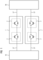
- the FIG 1 shows a known arrangement in which an energy source 55 is connected to a load 56 via two known electronic switches 7.
- the electronic switches 7 are arranged in the individual feeds 57, which electrically connect the energy source 55 to the load 56.
- This is, for example, a direct current network in which the energy source 55 and load 56 are connected to one another via two feeds 57, and in which a direct voltage is present between the two feeds 57.
- an electronic switch 7 is present in each of the two feeds 57.
- the electronic switch 7 in both feeds 57 can reliably switch off a current in just one of the two feeds 57, such as can occur in an earth fault, for example.
- the electronic switch 7 has a series connection of two semiconductor switches 2, which are arranged in a series connection.
- the semiconductor switches 2 have a switching element 21, which can conduct a current in one direction and switch it off.
- a diode 22 is arranged parallel to this switching element 21, which can conduct a current in the opposite direction but cannot switch it off.
- the diode 22 is thus arranged anti-parallel to the switching element 21.
- the semiconductor switches 2 are arranged anti-serially. Anti-serial means that a current in one direction can be switched off by the electronic switch 7 using one of the two semiconductor switches 2 and a current in the opposite direction can be switched off by the other of the two semiconductor switches 2.
- the FIG 2 shows an electronic circuit breaker 1.
- This has two semiconductor switches 2, in each of which the diode 22 is arranged antiparallel to the switching element 21.
- this has a total of four phase connections 31, 32, 41, 42.
- Two of these phase connections 31, 32 form the first mains connection 3, another two of these phase connections 41, 42 form the second mains connection 4.
- the two feeds to which the direct voltage is applied when used in a direct voltage network 6 are connected both at the first and the second mains connection 3, 4.
- the phase connections thus have 31, 32, 41, 42 have a positive potential and a negative potential of this direct voltage at the first mains connection 3 and at the second mains connection.
- positive potential connection 31, 41 and negative potential connection 32, 42 are referred to as positive potential connection 31, 41 and negative potential connection 32, 42. This designation will also be retained below if the electronic circuit breaker is used in an alternating voltage network and this involves a phase connection and a neutral conductor connection.
- the semiconductor switches 2 are arranged in the feed lines in such a way as to interrupt the flow of energy between the first mains connection 3 and the second mains connection 4. This interruption can be ensured for both energy flow directions, since the same current flows between the positive potential connection 31 of the first mains connection and the positive potential connection 41 of the second mains connection 4 as between the negative potential connection 32 of the first mains connection 3 and the negative potential connection 42 of the second mains connection 4.
- the currents only differ in their direction. This involves a forward current and a return current from the energy source to the load. In order to be able to interrupt the energy flow regardless of the direction of energy flow, the current flows once through the switching element 21 and once through the diode 22. The current can thus be interrupted regardless of the direction of energy flow.
- the first semiconductor switch can conduct and interrupt a current from the positive potential connection 31 of the first network connection 3 to the positive potential connection 41 of the second network connection 4 and the second semiconductor switch can conduct and interrupt a current from the negative potential connection 32 of the first network connection 3 to the negative potential connection 42 of the second network connection 4. This means that a current between the two energy sub-networks can be interrupted regardless of the direction of energy flow.
- the FIG 3 shows an energy network 5. Due to the two feeds between, this can be a direct current network 6, for example. Alternatively, it can also be designed as an alternating current network.
- This energy network 5 generally has a first energy sub-network 51 and a second energy sub-network 52. These are connected to one another via two feeds 57, with the electronic circuit breaker 1 being introduced into these feeds 57 in order to be able to separate the two sub-networks from one another or to connect them to one another.
- the energy sub-networks 51, 52 can have one or more energy sources (not shown in more detail) and/or one or more loads (not shown in more detail), such as electrical consumers. It is possible for the energy sub-networks to have a combination of energy sources and loads.
- one energy sub-network 51 is an energy source that is designed as a direct current source
- the second energy sub-network is a load that is supplied with a direct current.
- the energy flow between the two sub-networks can be interrupted regardless of the direction of energy flow.
- this arrangement can be used to detect and localize an error that occurs, in particular an earth fault, by measuring and evaluating the voltage at the respective potentials 31, 32, 41, 42 compared to the earth potential. This is particularly advantageous for use in an isolated DC voltage network.
- the invention relates to an electronic circuit breaker, having two semiconductor switches, each with a switching element and a diode arranged anti-parallel to the switching element.
- the electronic switch further have a first mains connection and a second mains connection, each with a positive potential connection and a negative potential connection, wherein a first of the semiconductor switches is arranged without a semiconductor series connection between the positive potential connection of the first mains connection and the positive potential connection of the second mains connection and a second of the semiconductor switches is arranged without a semiconductor series connection between the negative potential connection of the first mains connection and the negative potential connection of the second mains connection, wherein the switching element of the respective semiconductor switch is arranged in such a way that a current can be conducted from the first mains connection to the second mains connection and switched off.
- the invention further relates to an energy network, in particular a direct current network, with a first energy sub-network and a second energy sub-network, wherein the energy network has such an electronic circuit breaker for isolating the first energy sub-network and the second energy sub-network from one another, wherein the first energy sub-network is connected to the first network connection and the second energy sub-network is connected to the second network connection.
- the invention further relates to a method for operating such an energy network.
Landscapes
- Driving Mechanisms And Operating Circuits Of Arc-Extinguishing High-Tension Switches (AREA)
- Emergency Protection Circuit Devices (AREA)
- Protection Of Static Devices (AREA)
Claims (9)
- Interrupteur (1) électronique de protection d'un réseau à tension alternative monophasé ou triphasé, comportant- deux interrupteurs (2) à semiconducteur de même type ayant chacun un élément (21) de coupure et une diode (22) montée tête-bêche avec l'élément (21) de coupure et- une première borne (3) de réseau et une deuxième borne (4) de réseau ayant chacune une borne (31, 41) de potentiel positive et une borne (32, 42) de potentiel négative,dans lequel les interrupteurs à semiconducteur de même type sont de même type, dans lequel un premier des deux interrupteurs (2) à semiconducteur de même type est monté sans circuit série à semiconducteur entre la borne (31) de potentiel positive de la première borne (3) de réseau et la borne (41) de potentiel positive de la deuxième borne (4) de réseau et un deuxième des deux interrupteurs (2) à semiconducteur de même type est monté sans circuit série à semiconducteur entre la borne (32) de potentiel négative de la première borne (3) de réseau et la borne (42) de potentiel négative de la deuxième borne (4) de réseau, dans lequel l'élément (21) de coupure de l'interrupteur (2) à semiconducteur respectif est monté, de manière à ce qu'un courant puisse passer et être interrompu de la première borne (3) de réseau à la deuxième borne (4) de réseau, dans lequel les deux interrupteurs (2) à semiconducteur de même type sont formés chacun par un interrupteur à semiconducteur IGBT.
- Interrupteur (1) électronique de protection suivant la revendication 1, dans lequel l'interrupteur (1) électronique de protection a exactement deux interrupteurs (2) à semiconducteur pour la coupure d'un courant entre les bornes (3, 4) de réseau dans un réseau à tension alternative, dans lequel la borne (31) de potentiel positive est reliée à la phase et la borne (32) de potentiel négative au conducteur neutre.
- Interrupteur (1) électronique de protection suivant l'une des revendications 1 ou 2, dans lequel l'interrupteur (1) électronique de protection a respectivement une détection de tension pour la mesure d'une tension entre la borne (31) de potentiel positive de la première borne (3) du réseau et un potentiel de terre et/ou une tension entre la borne (32) de potentiel négative de la première borne (3) du réseau et le potentiel de terre et/ou une tension entre la borne (41) de potentiel positive de la deuxième borne (4) du réseau et le potentiel de terre et/ou une tension entre la borne (42) de potentiel négative de la deuxième borne (4) du réseau et le potentiel de terre.
- Interrupteur (1) électronique de protection suivant l'une des revendications 1 à 3, dans lequel les deux interrupteurs à semiconducteur de même type reposent respectivement par leur construction sur un transistor de type NPN.
- Réseau (5) d'énergie comprenant un premier réseau (51) partiel d'énergie et un deuxième réseau (52) partiel d'énergie, dans lequel le réseau (5) d'énergie a un interrupteur (1) électronique de protection suivant l'une des revendications 1 à 4, pour la séparation du premier réseau (51) partiel d'énergie et du deuxième réseau (52) partiel d'énergie l'un de l'autre, dans lequel le premier réseau (51) partiel d'énergie est relié à la première borne (3) du réseau et le deuxième réseau (52) partiel d'énergie est relié à la deuxième borne (4) du réseau.
- Réseau (5) suivant la revendication 5, dans lequel les réseaux (51, 52) partiels d'énergie ont une ou plusieurs charges inductives.
- Procédé pour faire fonctionner un réseau (5) d'énergie suivant l'une des revendications 5 ou 6, dans lequel à l'apparition d'une connexion à la terre dans le réseau (5) d'énergie, on ouvre l'interrupteur (1) électronique de protection.
- Procédé suivant la revendication 7, dans lequel, à partir de la mesure d'une tension entre la borne (31) de potentiel positive de la première borne (3) du réseau et un potentiel de terre et/ou d'une tension entre la borne (32) de potentiel négative de la première borne (3) du réseau et le potentiel de terre et/ou d'une tension entre la borne (41) de potentiel positive de la deuxième borne (4) du réseau et le potentiel de terre et/ou d'une tension entre la borne (42) de potentiel négative de la deuxième borne (4) du réseau et le potentiel de terre, on détermine l'emplacement du défaut.
- Utilisation d'un interrupteur électronique de protection suivant l'une des revendications 1 à 4, dans un réseau à tension alternative monophasé ou triphasé.
Applications Claiming Priority (2)
| Application Number | Priority Date | Filing Date | Title |
|---|---|---|---|
| EP19200185.7A EP3799306A1 (fr) | 2019-09-27 | 2019-09-27 | Commutateur de protection électronique |
| PCT/EP2020/072969 WO2021058197A1 (fr) | 2019-09-27 | 2020-08-17 | Disjoncteur électronique |
Publications (2)
| Publication Number | Publication Date |
|---|---|
| EP4010982A1 EP4010982A1 (fr) | 2022-06-15 |
| EP4010982B1 true EP4010982B1 (fr) | 2025-03-05 |
Family
ID=68084652
Family Applications (2)
| Application Number | Title | Priority Date | Filing Date |
|---|---|---|---|
| EP19200185.7A Withdrawn EP3799306A1 (fr) | 2019-09-27 | 2019-09-27 | Commutateur de protection électronique |
| EP20764031.9A Active EP4010982B1 (fr) | 2019-09-27 | 2020-08-17 | Commutateur de protection électronique |
Family Applications Before (1)
| Application Number | Title | Priority Date | Filing Date |
|---|---|---|---|
| EP19200185.7A Withdrawn EP3799306A1 (fr) | 2019-09-27 | 2019-09-27 | Commutateur de protection électronique |
Country Status (4)
| Country | Link |
|---|---|
| US (1) | US12283807B2 (fr) |
| EP (2) | EP3799306A1 (fr) |
| CN (1) | CN114514700B (fr) |
| WO (1) | WO2021058197A1 (fr) |
Families Citing this family (1)
| Publication number | Priority date | Publication date | Assignee | Title |
|---|---|---|---|---|
| EP4607730A1 (fr) * | 2024-02-23 | 2025-08-27 | FRONIUS INTERNATIONAL GmbH | Convertisseur sans transformateur avec protection contre les défauts de mise à la terre |
Citations (1)
| Publication number | Priority date | Publication date | Assignee | Title |
|---|---|---|---|---|
| EP2517351B1 (fr) * | 2009-12-21 | 2015-02-25 | Robert Bosch GmbH | Séparation du réseau électrique avec commutateurs pour outils électriques |
Family Cites Families (12)
| Publication number | Priority date | Publication date | Assignee | Title |
|---|---|---|---|---|
| WO2013131580A1 (fr) * | 2012-03-09 | 2013-09-12 | Siemens Aktiengesellschaft | Procédé pour connecter une section de réseau de tension continue à l'aide d'un interrupteur de tension continue |
| DE112012006912T5 (de) * | 2012-09-18 | 2015-05-28 | Aktiebolaget Skf | Schaltung zum Schützen einer elektrischen Last vor Gegenspannung und Überspannung, Verwendung einer solchen Schaltung zum Antreiben eines Drehsensors für ein instrumentiertes Lager und eine Lageranordnung, die eine solche Schaltung umfasst |
| US9853451B2 (en) | 2015-01-30 | 2017-12-26 | General Electric Company | Direct current power system |
| JP6662163B2 (ja) * | 2016-04-14 | 2020-03-11 | 富士電機株式会社 | 3レベルチョッパ装置 |
| GB201610901D0 (en) * | 2016-06-22 | 2016-08-03 | Eaton Ind Austria Gmbh | Hybrid DC circuit breaker |
| EP3379725A1 (fr) | 2017-03-23 | 2018-09-26 | Siemens Aktiengesellschaft | Procédé de commande d'un commutateur à courant continu, commutateur à courant continu et système de tension continue |
| CN109245038B (zh) * | 2017-07-10 | 2020-03-31 | 比亚迪股份有限公司 | 列车和列车供电系统及其漏电保护装置 |
| CN107592010A (zh) * | 2017-08-05 | 2018-01-16 | 天津大学 | 模块化多电平动态投切dc‑dc变压器 |
| US10985548B2 (en) * | 2018-10-01 | 2021-04-20 | Intelesol, Llc | Circuit interrupter with optical connection |
| US11349296B2 (en) * | 2018-10-01 | 2022-05-31 | Intelesol, Llc | Solid-state circuit interrupters |
| EP3691128A1 (fr) * | 2019-01-31 | 2020-08-05 | Siemens Aktiengesellschaft | Commutateur électronique |
| US11469757B2 (en) * | 2020-10-16 | 2022-10-11 | Abb Schweiz Ag | Solid-state power switch |
-
2019
- 2019-09-27 EP EP19200185.7A patent/EP3799306A1/fr not_active Withdrawn
-
2020
- 2020-08-17 EP EP20764031.9A patent/EP4010982B1/fr active Active
- 2020-08-17 CN CN202080067287.3A patent/CN114514700B/zh active Active
- 2020-08-17 US US17/763,390 patent/US12283807B2/en active Active
- 2020-08-17 WO PCT/EP2020/072969 patent/WO2021058197A1/fr not_active Ceased
Patent Citations (1)
| Publication number | Priority date | Publication date | Assignee | Title |
|---|---|---|---|---|
| EP2517351B1 (fr) * | 2009-12-21 | 2015-02-25 | Robert Bosch GmbH | Séparation du réseau électrique avec commutateurs pour outils électriques |
Also Published As
| Publication number | Publication date |
|---|---|
| US12283807B2 (en) | 2025-04-22 |
| WO2021058197A1 (fr) | 2021-04-01 |
| CN114514700B (zh) | 2026-02-17 |
| US20220344927A1 (en) | 2022-10-27 |
| EP4010982A1 (fr) | 2022-06-15 |
| CN114514700A (zh) | 2022-05-17 |
| EP3799306A1 (fr) | 2021-03-31 |
Similar Documents
| Publication | Publication Date | Title |
|---|---|---|
| EP3583695B1 (fr) | Procédé de commande d'un commutateur à courant continu, commutateur à courant continu et système de tension continue | |
| EP3257147B1 (fr) | Ensemble convertisseur et procédé de protection contre les court-circuits dudit ensemble convertisseur | |
| EP3552289B1 (fr) | Disjoncteur basse tension | |
| DE102019203977B4 (de) | Schutzschalteinrichtung für Gleichspannung und Gleichspannungsabzweig mit Schutzschalteinrichtung | |
| EP3639353B1 (fr) | Impédance pour controler des courants de défaut dans un convertisseur c.c.h.t. | |
| EP3743980A1 (fr) | Dispositif de commutation | |
| EP2523296A1 (fr) | Agencement de commutation pour la préparation d'une protection contre les surtensions et son procédé de fonctionnement | |
| EP3510617A1 (fr) | Disjoncteur | |
| EP3510620B1 (fr) | Disjoncteur | |
| EP3868021B1 (fr) | Commutateur électronique | |
| DE102021208466B4 (de) | Trennschaltereinheit | |
| EP3723223A1 (fr) | Emplacements d'une perte à la terre dans un réseau à courant continue | |
| EP4010982A1 (fr) | Disjoncteur électronique | |
| DE60001279T2 (de) | Erdfehler-schutzeinrichtung für die wicklung einer elektrischen maschine | |
| DE2026685C3 (de) | Verfahren und Schalteinrichtung zum Unterbrechen von Gleichstrom-Energieübertragungs netzen | |
| DE102015016232A1 (de) | Schaltbare Überspannungsschutzanordnung | |
| EP3048685B3 (fr) | Dispositif de protection de courant de fuite et procédé de commutation de contacts de commutation du dispositif de protection de courant de fuite | |
| DE102016110455A1 (de) | Überspannungsschutz für Wechselrichter | |
| BE1031299B1 (de) | Gleichspannungsschaltgerät, insbesondere zum Unterbrechen eines Stromflusses, und Gleichspannungssystem | |
| DE102006054940A1 (de) | Schaltfeldanlage mit Redundanz | |
| EP3609030A1 (fr) | Dispositif et procédé de coupure de court-circuit | |
| DE102023102239A1 (de) | Gleichspannungsschaltgerät, insbesondere zum Unterbrechen eines Stromflusses, und Gleichspannungssystem | |
| EP2810350B1 (fr) | Dispositif de distribution d' énergie | |
| DE888280C (de) | Schutzeinrichtung fuer Gleichstromuebertragungsleitungen | |
| DE19808595A1 (de) | Anordnung mit einem elektrischen Verbraucher in Reihe mit zwei steuerbaren Halbleiteranordnungen |
Legal Events
| Date | Code | Title | Description |
|---|---|---|---|
| STAA | Information on the status of an ep patent application or granted ep patent |
Free format text: STATUS: UNKNOWN |
|
| STAA | Information on the status of an ep patent application or granted ep patent |
Free format text: STATUS: THE INTERNATIONAL PUBLICATION HAS BEEN MADE |
|
| PUAI | Public reference made under article 153(3) epc to a published international application that has entered the european phase |
Free format text: ORIGINAL CODE: 0009012 |
|
| STAA | Information on the status of an ep patent application or granted ep patent |
Free format text: STATUS: REQUEST FOR EXAMINATION WAS MADE |
|
| 17P | Request for examination filed |
Effective date: 20220311 |
|
| AK | Designated contracting states |
Kind code of ref document: A1 Designated state(s): AL AT BE BG CH CY CZ DE DK EE ES FI FR GB GR HR HU IE IS IT LI LT LU LV MC MK MT NL NO PL PT RO RS SE SI SK SM TR |
|
| DAV | Request for validation of the european patent (deleted) | ||
| DAX | Request for extension of the european patent (deleted) | ||
| RAP1 | Party data changed (applicant data changed or rights of an application transferred) |
Owner name: INNOMOTICS GMBH |
|
| GRAP | Despatch of communication of intention to grant a patent |
Free format text: ORIGINAL CODE: EPIDOSNIGR1 |
|
| STAA | Information on the status of an ep patent application or granted ep patent |
Free format text: STATUS: GRANT OF PATENT IS INTENDED |
|
| INTG | Intention to grant announced |
Effective date: 20241023 |
|
| GRAS | Grant fee paid |
Free format text: ORIGINAL CODE: EPIDOSNIGR3 |
|
| GRAA | (expected) grant |
Free format text: ORIGINAL CODE: 0009210 |
|
| STAA | Information on the status of an ep patent application or granted ep patent |
Free format text: STATUS: THE PATENT HAS BEEN GRANTED |
|
| AK | Designated contracting states |
Kind code of ref document: B1 Designated state(s): AL AT BE BG CH CY CZ DE DK EE ES FI FR GB GR HR HU IE IS IT LI LT LU LV MC MK MT NL NO PL PT RO RS SE SI SK SM TR |
|
| REG | Reference to a national code |
Ref country code: GB Ref legal event code: FG4D Free format text: NOT ENGLISH |
|
| REG | Reference to a national code |
Ref country code: CH Ref legal event code: EP |
|
| REG | Reference to a national code |
Ref country code: IE Ref legal event code: FG4D Free format text: LANGUAGE OF EP DOCUMENT: GERMAN |
|
| REG | Reference to a national code |
Ref country code: DE Ref legal event code: R096 Ref document number: 502020010548 Country of ref document: DE |
|
| PG25 | Lapsed in a contracting state [announced via postgrant information from national office to epo] |
Ref country code: RS Free format text: LAPSE BECAUSE OF FAILURE TO SUBMIT A TRANSLATION OF THE DESCRIPTION OR TO PAY THE FEE WITHIN THE PRESCRIBED TIME-LIMIT Effective date: 20250605 |
|
| PG25 | Lapsed in a contracting state [announced via postgrant information from national office to epo] |
Ref country code: FI Free format text: LAPSE BECAUSE OF FAILURE TO SUBMIT A TRANSLATION OF THE DESCRIPTION OR TO PAY THE FEE WITHIN THE PRESCRIBED TIME-LIMIT Effective date: 20250305 |
|
| REG | Reference to a national code |
Ref country code: NL Ref legal event code: MP Effective date: 20250305 |
|
| PG25 | Lapsed in a contracting state [announced via postgrant information from national office to epo] |
Ref country code: ES Free format text: LAPSE BECAUSE OF FAILURE TO SUBMIT A TRANSLATION OF THE DESCRIPTION OR TO PAY THE FEE WITHIN THE PRESCRIBED TIME-LIMIT Effective date: 20250305 |
|
| REG | Reference to a national code |
Ref country code: LT Ref legal event code: MG9D |
|
| PG25 | Lapsed in a contracting state [announced via postgrant information from national office to epo] |
Ref country code: NO Free format text: LAPSE BECAUSE OF FAILURE TO SUBMIT A TRANSLATION OF THE DESCRIPTION OR TO PAY THE FEE WITHIN THE PRESCRIBED TIME-LIMIT Effective date: 20250605 |
|
| PG25 | Lapsed in a contracting state [announced via postgrant information from national office to epo] |
Ref country code: HR Free format text: LAPSE BECAUSE OF FAILURE TO SUBMIT A TRANSLATION OF THE DESCRIPTION OR TO PAY THE FEE WITHIN THE PRESCRIBED TIME-LIMIT Effective date: 20250305 |
|
| PG25 | Lapsed in a contracting state [announced via postgrant information from national office to epo] |
Ref country code: LV Free format text: LAPSE BECAUSE OF FAILURE TO SUBMIT A TRANSLATION OF THE DESCRIPTION OR TO PAY THE FEE WITHIN THE PRESCRIBED TIME-LIMIT Effective date: 20250305 |
|
| PG25 | Lapsed in a contracting state [announced via postgrant information from national office to epo] |
Ref country code: BG Free format text: LAPSE BECAUSE OF FAILURE TO SUBMIT A TRANSLATION OF THE DESCRIPTION OR TO PAY THE FEE WITHIN THE PRESCRIBED TIME-LIMIT Effective date: 20250305 Ref country code: GR Free format text: LAPSE BECAUSE OF FAILURE TO SUBMIT A TRANSLATION OF THE DESCRIPTION OR TO PAY THE FEE WITHIN THE PRESCRIBED TIME-LIMIT Effective date: 20250606 |
|
| PG25 | Lapsed in a contracting state [announced via postgrant information from national office to epo] |
Ref country code: NL Free format text: LAPSE BECAUSE OF FAILURE TO SUBMIT A TRANSLATION OF THE DESCRIPTION OR TO PAY THE FEE WITHIN THE PRESCRIBED TIME-LIMIT Effective date: 20250305 |
|
| PG25 | Lapsed in a contracting state [announced via postgrant information from national office to epo] |
Ref country code: SE Free format text: LAPSE BECAUSE OF FAILURE TO SUBMIT A TRANSLATION OF THE DESCRIPTION OR TO PAY THE FEE WITHIN THE PRESCRIBED TIME-LIMIT Effective date: 20250305 |
|
| PG25 | Lapsed in a contracting state [announced via postgrant information from national office to epo] |
Ref country code: SM Free format text: LAPSE BECAUSE OF FAILURE TO SUBMIT A TRANSLATION OF THE DESCRIPTION OR TO PAY THE FEE WITHIN THE PRESCRIBED TIME-LIMIT Effective date: 20250305 |
|
| PG25 | Lapsed in a contracting state [announced via postgrant information from national office to epo] |
Ref country code: PT Free format text: LAPSE BECAUSE OF FAILURE TO SUBMIT A TRANSLATION OF THE DESCRIPTION OR TO PAY THE FEE WITHIN THE PRESCRIBED TIME-LIMIT Effective date: 20250707 |
|
| PGFP | Annual fee paid to national office [announced via postgrant information from national office to epo] |
Ref country code: DE Payment date: 20250827 Year of fee payment: 6 |
|
| PG25 | Lapsed in a contracting state [announced via postgrant information from national office to epo] |
Ref country code: IT Free format text: LAPSE BECAUSE OF FAILURE TO SUBMIT A TRANSLATION OF THE DESCRIPTION OR TO PAY THE FEE WITHIN THE PRESCRIBED TIME-LIMIT Effective date: 20250305 Ref country code: PL Free format text: LAPSE BECAUSE OF FAILURE TO SUBMIT A TRANSLATION OF THE DESCRIPTION OR TO PAY THE FEE WITHIN THE PRESCRIBED TIME-LIMIT Effective date: 20250305 |
|
| PG25 | Lapsed in a contracting state [announced via postgrant information from national office to epo] |
Ref country code: EE Free format text: LAPSE BECAUSE OF FAILURE TO SUBMIT A TRANSLATION OF THE DESCRIPTION OR TO PAY THE FEE WITHIN THE PRESCRIBED TIME-LIMIT Effective date: 20250305 Ref country code: CZ Free format text: LAPSE BECAUSE OF FAILURE TO SUBMIT A TRANSLATION OF THE DESCRIPTION OR TO PAY THE FEE WITHIN THE PRESCRIBED TIME-LIMIT Effective date: 20250305 |
|
| PG25 | Lapsed in a contracting state [announced via postgrant information from national office to epo] |
Ref country code: RO Free format text: LAPSE BECAUSE OF FAILURE TO SUBMIT A TRANSLATION OF THE DESCRIPTION OR TO PAY THE FEE WITHIN THE PRESCRIBED TIME-LIMIT Effective date: 20250305 |
|
| PG25 | Lapsed in a contracting state [announced via postgrant information from national office to epo] |
Ref country code: SK Free format text: LAPSE BECAUSE OF FAILURE TO SUBMIT A TRANSLATION OF THE DESCRIPTION OR TO PAY THE FEE WITHIN THE PRESCRIBED TIME-LIMIT Effective date: 20250305 |
|
| PG25 | Lapsed in a contracting state [announced via postgrant information from national office to epo] |
Ref country code: IS Free format text: LAPSE BECAUSE OF FAILURE TO SUBMIT A TRANSLATION OF THE DESCRIPTION OR TO PAY THE FEE WITHIN THE PRESCRIBED TIME-LIMIT Effective date: 20250705 |
|
| REG | Reference to a national code |
Ref country code: DE Ref legal event code: R097 Ref document number: 502020010548 Country of ref document: DE |
|
| PLBE | No opposition filed within time limit |
Free format text: ORIGINAL CODE: 0009261 |
|
| STAA | Information on the status of an ep patent application or granted ep patent |
Free format text: STATUS: NO OPPOSITION FILED WITHIN TIME LIMIT |
|
| PG25 | Lapsed in a contracting state [announced via postgrant information from national office to epo] |
Ref country code: DK Free format text: LAPSE BECAUSE OF FAILURE TO SUBMIT A TRANSLATION OF THE DESCRIPTION OR TO PAY THE FEE WITHIN THE PRESCRIBED TIME-LIMIT Effective date: 20250305 |
|
| REG | Reference to a national code |
Ref country code: CH Ref legal event code: L10 Free format text: ST27 STATUS EVENT CODE: U-0-0-L10-L00 (AS PROVIDED BY THE NATIONAL OFFICE) Effective date: 20260114 |
|
| 26N | No opposition filed |
Effective date: 20251208 |
|
| REG | Reference to a national code |
Ref country code: CH Ref legal event code: H13 Free format text: ST27 STATUS EVENT CODE: U-0-0-H10-H13 (AS PROVIDED BY THE NATIONAL OFFICE) Effective date: 20260324 |
|
| PG25 | Lapsed in a contracting state [announced via postgrant information from national office to epo] |
Ref country code: MC Free format text: LAPSE BECAUSE OF FAILURE TO SUBMIT A TRANSLATION OF THE DESCRIPTION OR TO PAY THE FEE WITHIN THE PRESCRIBED TIME-LIMIT Effective date: 20250305 |
|
| PG25 | Lapsed in a contracting state [announced via postgrant information from national office to epo] |
Ref country code: LU Free format text: LAPSE BECAUSE OF NON-PAYMENT OF DUE FEES Effective date: 20250817 |
|
| PG25 | Lapsed in a contracting state [announced via postgrant information from national office to epo] |
Ref country code: CH Free format text: LAPSE BECAUSE OF NON-PAYMENT OF DUE FEES Effective date: 20250831 |
|
| GBPC | Gb: european patent ceased through non-payment of renewal fee |
Effective date: 20250817 |