EP4011017B1 - Appareil et procédé de traitement d'informations - Google Patents
Appareil et procédé de traitement d'informations Download PDFInfo
- Publication number
- EP4011017B1 EP4011017B1 EP20856331.2A EP20856331A EP4011017B1 EP 4011017 B1 EP4011017 B1 EP 4011017B1 EP 20856331 A EP20856331 A EP 20856331A EP 4011017 B1 EP4011017 B1 EP 4011017B1
- Authority
- EP
- European Patent Office
- Prior art keywords
- value
- harq
- cyclic shift
- ack information
- ack
- Prior art date
- Legal status (The legal status is an assumption and is not a legal conclusion. Google has not performed a legal analysis and makes no representation as to the accuracy of the status listed.)
- Active
Links
Images


Classifications
-
- H—ELECTRICITY
- H04—ELECTRIC COMMUNICATION TECHNIQUE
- H04L—TRANSMISSION OF DIGITAL INFORMATION, e.g. TELEGRAPHIC COMMUNICATION
- H04L5/00—Arrangements affording multiple use of the transmission path
- H04L5/003—Arrangements for allocating sub-channels of the transmission path
- H04L5/0053—Allocation of signalling, i.e. of overhead other than pilot signals
- H04L5/0055—Physical resource allocation for ACK/NACK
-
- H—ELECTRICITY
- H04—ELECTRIC COMMUNICATION TECHNIQUE
- H04W—WIRELESS COMMUNICATION NETWORKS
- H04W72/00—Local resource management
- H04W72/12—Wireless traffic scheduling
- H04W72/1263—Mapping of traffic onto schedule, e.g. scheduled allocation or multiplexing of flows
-
- H—ELECTRICITY
- H04—ELECTRIC COMMUNICATION TECHNIQUE
- H04L—TRANSMISSION OF DIGITAL INFORMATION, e.g. TELEGRAPHIC COMMUNICATION
- H04L1/00—Arrangements for detecting or preventing errors in the information received
- H04L1/0001—Systems modifying transmission characteristics according to link quality, e.g. power backoff
- H04L1/0002—Systems modifying transmission characteristics according to link quality, e.g. power backoff by adapting the transmission rate
- H04L1/0003—Systems modifying transmission characteristics according to link quality, e.g. power backoff by adapting the transmission rate by switching between different modulation schemes
-
- H—ELECTRICITY
- H04—ELECTRIC COMMUNICATION TECHNIQUE
- H04L—TRANSMISSION OF DIGITAL INFORMATION, e.g. TELEGRAPHIC COMMUNICATION
- H04L1/00—Arrangements for detecting or preventing errors in the information received
- H04L1/12—Arrangements for detecting or preventing errors in the information received by using return channel
- H04L1/16—Arrangements for detecting or preventing errors in the information received by using return channel in which the return channel carries supervisory signals, e.g. repetition request signals
- H04L1/18—Automatic repetition systems, e.g. Van Duuren systems
- H04L1/1812—Hybrid protocols; Hybrid automatic repeat request [HARQ]
-
- H—ELECTRICITY
- H04—ELECTRIC COMMUNICATION TECHNIQUE
- H04L—TRANSMISSION OF DIGITAL INFORMATION, e.g. TELEGRAPHIC COMMUNICATION
- H04L1/00—Arrangements for detecting or preventing errors in the information received
- H04L1/12—Arrangements for detecting or preventing errors in the information received by using return channel
- H04L1/16—Arrangements for detecting or preventing errors in the information received by using return channel in which the return channel carries supervisory signals, e.g. repetition request signals
- H04L1/18—Automatic repetition systems, e.g. Van Duuren systems
- H04L1/1829—Arrangements specially adapted for the receiver end
- H04L1/1861—Physical mapping arrangements
-
- H—ELECTRICITY
- H04—ELECTRIC COMMUNICATION TECHNIQUE
- H04L—TRANSMISSION OF DIGITAL INFORMATION, e.g. TELEGRAPHIC COMMUNICATION
- H04L27/00—Modulated-carrier systems
- H04L27/26—Systems using multi-frequency codes
- H04L27/2601—Multicarrier modulation systems
- H04L27/2602—Signal structure
- H04L27/2605—Symbol extensions, e.g. Zero Tail, Unique Word [UW]
- H04L27/2607—Cyclic extensions
-
- H—ELECTRICITY
- H04—ELECTRIC COMMUNICATION TECHNIQUE
- H04L—TRANSMISSION OF DIGITAL INFORMATION, e.g. TELEGRAPHIC COMMUNICATION
- H04L27/00—Modulated-carrier systems
- H04L27/26—Systems using multi-frequency codes
- H04L27/2601—Multicarrier modulation systems
- H04L27/2614—Peak power aspects
-
- H—ELECTRICITY
- H04—ELECTRIC COMMUNICATION TECHNIQUE
- H04L—TRANSMISSION OF DIGITAL INFORMATION, e.g. TELEGRAPHIC COMMUNICATION
- H04L5/00—Arrangements affording multiple use of the transmission path
- H04L5/003—Arrangements for allocating sub-channels of the transmission path
- H04L5/0053—Allocation of signalling, i.e. of overhead other than pilot signals
-
- H—ELECTRICITY
- H04—ELECTRIC COMMUNICATION TECHNIQUE
- H04W—WIRELESS COMMUNICATION NETWORKS
- H04W72/00—Local resource management
- H04W72/04—Wireless resource allocation
- H04W72/044—Wireless resource allocation based on the type of the allocated resource
- H04W72/0453—Resources in frequency domain, e.g. a carrier in FDMA
-
- H—ELECTRICITY
- H04—ELECTRIC COMMUNICATION TECHNIQUE
- H04L—TRANSMISSION OF DIGITAL INFORMATION, e.g. TELEGRAPHIC COMMUNICATION
- H04L1/00—Arrangements for detecting or preventing errors in the information received
- H04L1/12—Arrangements for detecting or preventing errors in the information received by using return channel
- H04L1/16—Arrangements for detecting or preventing errors in the information received by using return channel in which the return channel carries supervisory signals, e.g. repetition request signals
- H04L1/1607—Details of the supervisory signal
- H04L1/1671—Details of the supervisory signal the supervisory signal being transmitted together with control information
Definitions
- the present disclosure relates to the field of communication systems, and more particularly, to an apparatus and an information processing method, which can provide a good communication performance and high reliability.
- Wireless communication systems are widely deployed to provide various types of communication content such as voice, data, and so on.
- the wireless communication systems may be multiple-access systems capable of supporting communication with multiple users by sharing the available system resources (e.g., bandwidth and transmit power).
- Examples of such multiple-access systems include code division multiple access (CDMA) systems, time division multiple access (TDMA) systems, frequency division multiple access (FDMA) systems, 3rd generation partnership project (3GPP) long term evolution (LTE) systems, and orthogonal frequency division multiple access (OFDMA) systems.
- CDMA code division multiple access
- TDMA time division multiple access
- FDMA frequency division multiple access
- 3GPP 3rd generation partnership project
- LTE long term evolution
- OFDMA orthogonal frequency division multiple access
- an unlicensed spectrum is a shared spectrum.
- Communication equipments in different communication systems can use the unlicensed spectrum as long as the unlicensed meets regulatory requirements set by countries or regions on a spectrum. There is no need to apply for a proprietary spectrum authorization from a government.
- a communication device follows a listen before talk (LBT) procedure, that is, the communication device needs to perform a channel sensing before transmitting a signal on a channel.
- LBT listen before talk
- an LBT outcome illustrates that the channel is idle
- the communication device can perform signal transmission, otherwise, the communication device cannot perform signal transmission.
- MCOT maximum channel occupancy time
- a base station On an unlicensed carrier, for a channel occupation time obtained by a base station, it may share the channel occupation time to a user equipment (UE) for transmitting an uplink signal or an uplink channel.
- UE user equipment
- the base station shares its own channel occupancy time with the UE, the UE can use an LBT mode with higher priority than that used by the UE itself to obtain the channel, thereby obtaining the channel with greater probability.
- a wideband operation can be configured and a configured active bandwidth part (BWP) can include resource block sets (RB sets).
- BWP active bandwidth part
- RB sets resource block sets
- PUCCH Physical uplink control channel
- a BS such as gNB
- a UE can operate in a wider band including RB sets.
- NR release 15 has defined a BWP concept, thus in a context of the NRU wideband operation, the UE can be configured with an active BWP including multiple RB sets. Multiple RB sets can be assigned by the gNB to the UE for uplink transmission, e.g. a physical uplink control channel (PUCCH) transmission.
- PUCCH physical uplink control channel
- FIG. 1 illustrates an interlaced structure for an uplink channel transmission.
- NRU new radio-based access to unlicensed spectrum
- PUCCH physical uplink control channel
- PUSCH physical uplink shared channel
- This channel can carrier up to 2-bit positive-acknowledgement (ACK)/negative-acknowledgement (NACK) information together with scheduling request (SR) indication.
- ACK/NACK information is presented by a cyclic shift (CS), additionally introduced on top of the CGS.
- the ACK/NACK information is tightly bounded with the m cs value, which is specified in NR release 15, 38.213 section 9.2.3 and section 9.2.5.1.
- the PUCCH format 0 occupies 1 PRB in frequency domain (12 subcarriers) and 1 or 2 orthogonal frequency division multiplexing (OFDM) symbols in time domain.
- ⁇ is actually a cyclic shift through which a PUCCH transmitted on an interlace can be generated.
- n s ,f ⁇ is the slot number in the radio frame
- l is the OFDM symbol number in the PUCCH transmission
- l' is the index of the OFDM symbol in the slot that corresponds to the first OFDM symbol of the PUCCH transmission in the slot given by [5, TS 38.213]
- m 0 is given by [5, TS 38.213] for PUCCH format 0 and 1 while for PUCCH format 3 and 4 is defined in subclause 6.4.1.3.3.1
- m cs 0 except for PUCCH format 0 when it depends on the information to be transmitted according to subclause 9.2
- the NR release15 PUCCH format 0 occupies only 1 PRB in frequency domain; while in new radio-based access to unlicensed spectrum (NRU), an interlaced structure should be implemented, so that PUCCH format 0 can be transmitted on multiple PRBs (such as 10 or 11 PRBs) in an interlace. If PUCCH format 0 simply repeats transmission on each of the PRBs multiple times, the content transmitted on each of the PRBs has the same cyclic shift. A simple repetition of NR release 15 PUCCH format 0 in each of the PRBs of an interlace will cause a very high peak to average power ratio (PAPR) issue. Thus, an enhancement should be done for this new design of PUCCH format 0 in NRU systems.
- PAPR peak to average power ratio
- some embodiments of the present disclosure provide a method of designing an NRU PUCCH format 0. Some embodiments of the present disclosure further provide technical solutions to resolve this issue.
- PUCCH format 0 on each of the PRBs is given as different cyclic shift as possible, so that data in each of the PRBs is no longer completely the same, and the high PAPR issue can be avoided as much as possible.
- FIG. 2 illustrates that, in some embodiments, a user equipment (UE) 10 and a base station (BS) (e.g., gNB) 20 of communication in a communication network system 30 according to an embodiment of the present disclosure are provided.
- the communication network system 30 includes one or more UEs 10 of a cell and the BS 20.
- the UE 10 may include a memory 12, a transceiver 13, and a processor 11 coupled to the memory 12, the transceiver 13.
- the base station 20 may include a memory 22, a transceiver 23, and a processor 21 coupled to the memory 22, the transceiver 23.
- the processor 11 or 21 may be configured to implement proposed functions, procedures and/or methods described in this description. Layers of radio interface protocol may be implemented in the processor 11 or 21.
- the memory 12 or 22 is operatively coupled with the processor 11 or 21 and stores a variety of first information to operate the processor 11 or 21.
- the transceiver 13 or 23 is operatively coupled with the processor 11 or 21, and the transceiver 13 or 23 transmits and/or receives a radio signal.
- the processor 11 or 21 may include application-specific integrated circuit (ASIC), other chipset, logic circuit and/or data processing device.
- the memory 12 or 22 may include read-only memory (ROM), random access memory (RAM), flash memory, memory card, storage medium and/or other storage device.
- the transceiver 13 or 23 may include baseband circuitry to process radio frequency signals.
- modules e.g., procedures, functions, and so on
- the modules can be stored in the memory 12 or 22 and executed by the processor 11 or 21.
- the memory 12 or 22 can be implemented within the processor 11 or 21 or external to the processor 11 or 21 in which case those can be communicatively coupled to the processor 11 or 21 via various means as is known in the art.
- the processor 11 is configured to determine a cyclic shift sequence comprising N cyclic shifts according to a hybrid automatic repeat request acknowledgement (HARQ-ACK) information to be transmitted and/or a scheduling request (SR) to be transmitted, wherein a resource in a frequency domain used for transmitting the HARQ-ACK information to be transmitted and/or the SR to be transmitted is a target interlace, the target interlace comprises N physical resource blocks (PRBs), the N cyclic shifts have a one-to-one correspondence with the N PRBs, and N is an integer and greater than 1.
- the processor 11 is configured to generate a target physical uplink control channel (PUCCH) based on PUCCH format_0 according to the cyclic shift sequence.
- PUCCH physical uplink control channel
- the transceiver 13 is configured to transmit the target PUCCH on the target interlace. This can solve issues in the prior art, provide a generation process of an interlaced control channel and further maintain a low peak-to-average power ratio (PAPR) property. Further, PUCCH format 0 on each of the PRBs is given as different cyclic shift as possible, so that data in each of the PRBs is no longer completely the same, and the high PAPR issue can be avoided as much as possible.
- PAPR peak-to-average power ratio
- the processor 21 is configured to: parse a target physical uplink control channel (PUCCH) on a target interlace based on PUCCH format_0 according to a cyclic shift sequence comprising N cyclic shifts; obtain modulation and coding scheme (MCS)-0 by parsing the cyclic shift sequence; and obtain a hybrid automatic repeat request acknowledgement (HARQ-ACK) information and/or a scheduling request (SR) on the PUCCH, wherein a resource in a frequency domain used for transmitting the HARQ-ACK information and/or the SR is the target interlace, the target interlace comprises N physical resource blocks (PRBs), the N cyclic shifts have a one-to-one correspondence with the N PRBs, and N is an integer and greater than 1.
- PUCCH physical uplink control channel
- MCS modulation and coding scheme
- SR scheduling request
- PUCCH format 0 on each of the PRBs is given as different cyclic shift as possible, so that data in each of the PRBs is no longer completely the same, and the high PAPR issue can be avoided as much as possible.
- the N cyclic shifts are in sequence from ⁇ 0 to ⁇ N- 1
- the N PRBs are in sequence from PRB 0 to PRB N- 1
- the one-to-one correspondence between the N cyclic shifts and the N PRBs comprises: ⁇ i in the cyclic shift sequence corresponds to PRB i in the N PRBs, and a value range of i is [0, N -1].
- the cyclic shift sequence is obtained from m cs parameter sequence
- the m cs parameter sequence comprises N m cs parameters
- the N cyclic shifts have a one-to-one correspondence with the N m cs parameters.
- the N m cs parameters are in sequence from m cs 0 to m cs N ⁇ 1 , the one-to-one correspondence between the N cyclic shifts and the N m cs parameters comprises: ⁇ i in the cyclic shift sequence corresponds to m cs i in the m cs parameter sequence, and a value range of i is [0, N -1].
- the SR comprises one of the followings: a negative SR or a positive SR.
- a starting element of the m cs parameter sequence is m cs 0
- a value of m cs 0 is associated with the HARQ-ACK information and/or the SR.
- a length of the HARQ-ACK information is 1 bit and a value is 0, or the SR is a negative SR and the length of the HARQ-ACK information is 1 bit and the value is 0, the value of m cs 0 is 0; and if the length of the HARQ-ACK information is 1 bit and the value is 1, or the SR is the negative SR and the length of the HARQ-ACK information is 1 bit and the value is 1, the value of m cs 0 is 6.
- a length of the HARQ-ACK information is 2 bits and a value is ⁇ 0, 0 ⁇ , or the SR is a negative SR and the length of the HARQ-ACK information is 2 bits and the value is ⁇ 0, 0 ⁇ , the value of m cs 0 is 0; if the length of the HARQ-ACK information is 2 bits and the value is ⁇ 0, 1 ⁇ , or the SR is the negative SR and the length of the HARQ-ACK information is 2 bits and the value is ⁇ 0, 1 ⁇ , the value of m cs 0 is 3; if the length of the HARQ-ACK information is 2 bits and the value is ⁇ 1, 1 ⁇ , or the SR is the negative SR and the length of the HARQ-ACK information is 2 bits and the value is ⁇ 1, 1 ⁇ , the value of m cs 0 is 6; and if the length of the HARQ-ACK information is 2 bits and the value is ⁇ 1, 0 ⁇ ,
- the SR is a positive SR, and a length of the HARQ-ACK information is 1 bit and a value is 0, the value of m cs 0 is 3; and if the SR is the positive SR, and the length of the HARQ-ACK information is 1 bit and the value is 1, the value of m cs 0 is 9.
- the SR is a positive SR, and a length of the HARQ-ACK information is 2 bits and a value is ⁇ 0, 0 ⁇ , the value of m cs 0 is 1; if the SR is the positive SR, and the length of the HARQ-ACK information is 2 bits and the value is ⁇ 0, 1 ⁇ , the value of m cs 0 is 4; if the SR is the positive SR, and the length of the HARQ-ACK information is 2 bits and the value is ⁇ 1, 1 ⁇ , the value of m cs 0 is 7; and if the SR is the positive SR, and the length of the HARQ-ACK information is 2 bits and the value is ⁇ 1, 0 ⁇ , the value of m cs 0 is 10.
- the processor 11 is configured to perform a generation process of an interlaced control channel, wherein the generation process of the interlaced control channel comprises at least one of the followings: determining a first cyclic shift member in a group; determining a cyclic shift group; or a cyclic shift group sequence to interlace mapping.
- the generation process of the interlaced control channel comprises at least one of the followings: determining a first cyclic shift member in a group; determining a cyclic shift group; or a cyclic shift group sequence to interlace mapping.
- PAPR peak-to-average power ratio
- determining the first cyclic shift member in the group is relevant to a positive-acknowledgement (ACK) information and/or a negative-acknowledgement (NACK) information. In some embodiments, determining the cyclic shift group is for a pair of ACK information, NACK information, and scheduling request (SR) information. In some embodiments, the ACK information corresponds to a first cyclic shift group, and the NACK information corresponds to a second cyclic shift group. In some embodiments, the first cyclic shift group and the second cyclic shift group have at least one different cyclic shift member in the group. In some embodiments, the first cyclic shift group and the second cyclic shift group have different cyclic shift member orderings. In some embodiments, the first cyclic shift group and the second cyclic shift group have the same cyclic shift members but with different cyclic shift member orderings.
- the transmission of the ACK information and the SR information corresponds to a third cyclic shift group which is obtained from the first cyclic shift group, such that the first cyclic shift group and the third cyclic shift group have the same cyclic shift members but different cyclic shift member orderings.
- the transmission of the NACK information and the SR information corresponds to a fourth cyclic shift group which is obtained from the second cyclic shift group, such that the second cyclic shift group and the fourth cyclic shift group have the same cyclic shift members but different cyclic shift member orderings.
- the processor 11 determines a first cyclic shift group, where a first cyclic shift member of a first cyclic shift group has value 0. In some embodiments, if the transceiver transmits 13 1-bit HARQ-ACK value 1 or 1-bit HARQ-ACK value 1 and a negative SR information, the processor 11 determines a second cyclic shift group, where a first cyclic shift member of a second cyclic shift group has value 6.
- HARQ-ACK hybrid automatic repeat request acknowledgement
- the processor 11 determines a third cyclic shift group, where a first cyclic shift member of a third cyclic shift group has value 0. In some embodiments, if the transceiver 13 transmits 2-bit HARQ-ACK value ⁇ 0,1 ⁇ or 2-bit HARQ-ACK value ⁇ 0,1 ⁇ and a negative SR information, the processor 11 determines a fourth cyclic shift group, where a first cyclic shift member of a fourth cyclic shift group has value 3.
- the processor 11 determines a fifth cyclic shift group, where a first cyclic shift member of the fifth cyclic shift group has value 6. In some embodiments, if the transceiver 13 transmits 2-bit HARQ-ACK value ⁇ 1,0 ⁇ or 2-bit HARQ ACK value ⁇ 1,0 ⁇ and a negative SR information, the processor 11 determines a sixth cyclic shift group, where a first cyclic shift member of the sixth cyclic shift group has value 9.
- the processor 11 determines a seventh cyclic shift group, where a first cyclic shift member of the seventh cyclic shift group has value 0 or value 3. In some embodiments, if the transceiver 13 transmits 1-bit HARQ ACK value 1 and a positive SR information, the processor 11 determines an eighth cyclic shift group, where a first cyclic shift member of the eighth cyclic shift group has value 6 or value 9.
- the processor 11 determines a ninth cyclic shift group, where a first cyclic shift member of the ninth cyclic shift group has value 0 or value. In some embodiments, if the transceiver 13 transmits 2-bit HARQ ACK value ⁇ 0,1 ⁇ and a positive SR information, the processor 11 determines a tenth cyclic shift group, where a first cyclic shift member of the tenth cyclic shift group has value 3 or value 4.
- the processor 11 determines an eleventh cyclic shift group #11, where a first cyclic shift member of the eleventh cyclic shift group has value 6 or value 7. In some embodiments, if the transceiver 13 transmits 2-bit HARQ ACK value ⁇ 1,0 ⁇ and a positive SR information, the processor 11 determines a twelfth cyclic shift group, where a first cyclic shift member of the twelfth cyclic shift group has value 9 or value 10.
- FIG. 3 illustrates a method 300 of communication of a UE according to an embodiment of the present disclosure.
- the method 300 includes: a block 302, performing, by the UE, a generation process of an interlaced control channel, wherein the generation process of the interlaced control channel comprises at least one of the followings: determining a first cyclic shift member in a group; determining a cyclic shift group; or a cyclic shift group sequence to interlace mapping.
- PAPR peak-to-average power ratio
- FIG. 4 illustrates an information processing method 400 of a UE according to an embodiment of the present disclosure.
- the method 400 includes: a block 402, determining, by a user equipment, a cyclic shift sequence comprising N cyclic shifts according to a hybrid automatic repeat request acknowledgement (HARQ-ACK) information to be transmitted and/or a scheduling request (SR) to be transmitted, wherein a resource in a frequency domain used for transmitting the HARQ-ACK information to be transmitted and/or the SR to be transmitted is a target interlace, the target interlace comprises N physical resource blocks (PRBs), the N cyclic shifts have a one-to-one correspondence with the N PRBs, and N is an integer and greater than 1, a block 404, generating, by the user equipment, a target physical uplink control channel (PUCCH) based on PUCCH format_0 according to the cyclic shift sequence, and a block 406, transmitting, by the user equipment, the target PUCCH on the target interlace.
- PUCCH format 0 on each of the PRBs is given as different cyclic shift as possible, so that data in each of the PRBs is no longer completely the same, and the high PAPR issue can be avoided as much as possible.
- FIG. 5 illustrates an information processing method 500 of a BS according to an embodiment of the present disclosure.
- the method 500 includes: a block 502, parsing, by a base station, a target physical uplink control channel (PUCCH) on a target interlace based on PUCCH format_0 according to a cyclic shift sequence comprising N cyclic shifts, a block 504, obtaining, by the base station, modulation and coding scheme (MCS)-0 by parsing the cyclic shift sequence, and a block 406, obtaining, by the base station, a hybrid automatic repeat request acknowledgement (HARQ-ACK) information and/or a scheduling request (SR) on the PUCCH, wherein a resource in a frequency domain used for transmitting the HARQ-ACK information and/or the SR is the target interlace, the target interlace comprises N physical resource blocks (PRBs), the N cyclic shifts have a one-to-one correspondence with the N PRBs, and N is an integer and greater than 1.
- PUCCH format 0 on each of the PRBs is given as different cyclic shift as possible, so that data in each of the PRBs is no longer completely the same, and the high PAPR issue can be avoided as much as possible.
- the N cyclic shifts are in sequence from ⁇ 0 to ⁇ N -1
- the N PRBs are in sequence from PRB 0 to PRB N -1
- the one-to-one correspondence between the N cyclic shifts and the N PRBs comprises: ⁇ i in the cyclic shift sequence corresponds to PRB i in the N PRBs, and a value range of i is [0, N -1].
- the cyclic shift sequence is obtained from m cs parameter sequence
- the m cs parameter sequence comprises N m cs parameters
- the N cyclic shifts have a one-to-one correspondence with the N m cs parameters.
- the N m cs parameters are in sequence from m cs 0 to m cs N ⁇ 1 , the one-to-one correspondence between the N cyclic shifts and the N m cs parameters comprises: ⁇ i in the cyclic shift sequence corresponds to m cs i in the m cs parameter sequence, and a value range of i is [0, N -1]1.
- the SR comprises one of the followings: a negative SR or a positive SR.
- a starting element of the m cs parameter sequence is m cs 0
- a value of m cs 0 is associated with the HARQ-ACK information and/or the SR.
- a length of the HARQ-ACK information is 1 bit and a value is 0, or the SR is a negative SR and the length of the HARQ-ACK information is 1 bit and the value is 0, the value of m cs 0 is 0; and if the length of the HARQ-ACK information is 1 bit and the value is 1, or the SR is the negative SR and the length of the HARQ-ACK information is 1 bit and the value is 1, the value of m cs 0 is 6.
- a length of the HARQ-ACK information is 2 bits and a value is ⁇ 0, 0 ⁇ , or the SR is a negative SR and the length of the HARQ-ACK information is 2 bits and the value is ⁇ 0, 0 ⁇ , the value of m cs 0 is 0; if the length of the HARQ-ACK information is 2 bits and the value is ⁇ 0, 1 ⁇ , or the SR is the negative SR and the length of the HARQ-ACK information is 2 bits and the value is ⁇ 0, 1 ⁇ , the value of m cs 0 is 3; if the length of the HARQ-ACK information is 2 bits and the value is ⁇ 1, 1 ⁇ , or the SR is the negative SR and the length of the HARQ-ACK information is 2 bits and the value is ⁇ 1, 1 ⁇ , the value of m cs 0 is 6; and if the length of the HARQ-ACK information is 2 bits and the value is ⁇ 1, 0 ⁇ ,
- the SR is a positive SR, and a length of the HARQ-ACK information is 1 bit and a value is 0, the value of m cs 0 is 3; and if the SR is the positive SR, and the length of the HARQ-ACK information is 1 bit and the value is 1, the value of m cs 0 is 9.
- the SR is a positive SR, and a length of the HARQ-ACK information is 2 bits and a value is ⁇ 0, 0 ⁇ , the value of m cs 0 is 1; if the SR is the positive SR, and the length of the HARQ-ACK information is 2 bits and the value is ⁇ 0, 1 ⁇ , the value of m cs 0 is 4; if the SR is the positive SR, and the length of the HARQ-ACK information is 2 bits and the value is ⁇ 1, 1 ⁇ , the value of m cs 0 is 7; and if the SR is the positive SR, and the length of the HARQ-ACK information is 2 bits and the value is ⁇ 1, 0 ⁇ , the value of m cs 0 is 10.
- determining the first cyclic shift member in the group is relevant to a positive-acknowledgement (ACK) information and/or a negative-acknowledgement (NACK) information. In some embodiments, determining the cyclic shift group is for a pair of ACK information, NACK information, and scheduling request (SR) information. In some embodiments, the ACK information corresponds to a first cyclic shift group, and the NACK information corresponds to a second cyclic shift group. In some embodiments, the first cyclic shift group and the second cyclic shift group have at least one different cyclic shift member in the group. In some embodiments, the first cyclic shift group and the second cyclic shift group have different cyclic shift member orderings. In some embodiments, the first cyclic shift group and the second cyclic shift group have the same cyclic shift members but with different cyclic shift member orderings.
- the transmission of the ACK information and the SR information corresponds to a third cyclic shift group which is obtained from the first cyclic shift group, such that the first cyclic shift group and the third cyclic shift group have the same cyclic shift members but different cyclic shift member orderings.
- the transmission of the NACK information and the SR information corresponds to a fourth cyclic shift group which is obtained from the second cyclic shift group, such that the second cyclic shift group and the fourth cyclic shift group have the same cyclic shift members but different cyclic shift member orderings.
- the UE determines a first cyclic shift group, where a first cyclic shift member of a first cyclic shift group has value 0. In some embodiments, if the UE transmits 1-bit HARQ-ACK value 1 or 1-bit HARQ-ACK value 1 and a negative SR information, the UE determines a second cyclic shift group, where a first cyclic shift member of a second cyclic shift group has value 6.
- HARQ-ACK hybrid automatic repeat request acknowledgement
- the UE determines a third cyclic shift group, where a first cyclic shift member of a third cyclic shift group has value 0. In some embodiments, if the UE transmits 2-bit HARQ-ACK value ⁇ 0,1 ⁇ or 2-bit HARQ-ACK value ⁇ 0,1 ⁇ and a negative SR information, the UE determines a fourth cyclic shift group, where a first cyclic shift member of a fourth cyclic shift group has value 3.
- the UE determines a fifth cyclic shift group, where a first cyclic shift member of the fifth cyclic shift group has value 6. In some embodiments, if the UE transmits 2-bit HARQ-ACK value ⁇ 1,0 ⁇ or 2-bit HARQ ACK value ⁇ 1,0 ⁇ and a negative SR information, the UE determines a sixth cyclic shift group, where a first cyclic shift member of the sixth cyclic shift group has value 9.
- the UE determines a seventh cyclic shift group, where a first cyclic shift member of the seventh cyclic shift group has value 0 or value 3. In some embodiments, if the UE transmits 1-bit HARQ ACK value 1 and a positive SR information, the UE determines an eighth cyclic shift group, where a first cyclic shift member of the eighth cyclic shift group has value 6 or value 9.
- the UE determines a ninth cyclic shift group, where a first cyclic shift member of the ninth cyclic shift group has value 0 or value. In some embodiments, if the UE transmits 2-bit HARQ ACK value ⁇ 0,1 ⁇ and a positive SR information, the UE determines a tenth cyclic shift group, where a first cyclic shift member of the tenth cyclic shift group has value 3 or value 4.
- the UE determines an eleventh cyclic shift group #11, where a first cyclic shift member of the eleventh cyclic shift group has value 6 or value 7. In some embodiments, if the UE transmits 2-bit HARQ ACK value ⁇ 1,0 ⁇ and a positive SR information, the UE determines a twelfth cyclic shift group, where a first cyclic shift member of the twelfth cyclic shift group has value 9 or value 10.
- Some embodiments of the present disclosure provide how to design a PUCCH format 0 in an interlaced structure and how it carries ACK/NACK and SR information. Some embodiments of the present disclosure include at least parts of the following.
- ACK corresponds to a first cyclic shift group
- NACK corresponds to a second cyclic shift group
- the first cyclic shift group and the second cyclic shift group have at least one different cyclic shift member in the group; or the first cyclic shift group and the second cyclic shift group have different cyclic shift member orderings; or the first cyclic shift group and the second cyclic shift group have the same cyclic shift members but with different cyclic shift member orderings; or for ACK+SR transmission, ACK+SR corresponds to a third cyclic shift group which is obtained from the first cyclic shift group, such that the first cyclic shift group and the third cyclic shift group have the same cyclic shift members but different cyclic shift member ordering; or for NACK+SR transmission, NACK+SR corresponds to a fourth cyclic shift group which is obtained from the second cyclic shift group, such that the second cyclic shift group and the fourth cyclic shift group have the same cyclic shift members but different cyclic shift member ordering.
- a UE wants to transmit 1-bit HARQ-ACK value 0 or 1-bit HARQ ACK value 0 + negative SR, the UE determines the cyclic shift group #1, where the first cyclic shift member of the cyclic shift group #1 has value 0. If a UE wants to transmit 1-bit HARQ-ACK value 1 or 1-bit HARQ ACK value 1 + negative SR, the UE determines the cyclic shift group #2, where the first cyclic shift member of the cyclic shift group #2 has value 6.
- a UE wants to transmit 2-bit HARQ-ACK value ⁇ 0,0 ⁇ or 2-bit HARQ ACK value ⁇ 0,0 ⁇ + negative SR, the UE determines the cyclic shift group #3, where the first cyclic shift member of the cyclic shift group #3 has value 0. If a UE wants to transmit 2-bit HARQ-ACK value ⁇ 0,1 ⁇ or 2-bit HARQ ACK value ⁇ 0,1 ⁇ + negative SR, the UE determines the cyclic shift group #4, where the first cyclic shift member of the cyclic shift group #4 has value 3.
- a UE wants to transmit 2-bit HARQ-ACK value ⁇ 1,1 ⁇ or 2-bit HARQ ACK value ⁇ 1,1 ⁇ + negative SR, the UE determines the cyclic shift group #5, where the first cyclic shift member of the cyclic shift group #5 has value 6. If a UE wants to transmit 2-bit HARQ-ACK value ⁇ 1,0 ⁇ or 2-bit HARQ ACK value ⁇ 1,0 ⁇ + negative SR, the UE determines the cyclic shift group #6, where the first cyclic shift member of the cyclic shift group #6 has value 9.
- a UE wants to transmit 1-bit HARQ ACK value 0 + positive SR, the UE determines the cyclic shift group #7, where the first cyclic shift member of the cyclic shift group #7 has value 0 or value 3. If a UE wants to transmit 1-bit HARQ ACK value 1 + positive SR, the UE determines the cyclic shift group #8, where the first cyclic shift member of the cyclic shift group #8 has value 6 or value 9. If a UE wants to transmit 2-bit HARQ ACK value ⁇ 0,0 ⁇ + positive SR, the UE determines the cyclic shift group #9, where the first cyclic shift member of the cyclic shift group #9 has value 0 or value 1.
- a UE wants to transmit 2-bit HARQ ACK value ⁇ 0,1 ⁇ + positive SR, the UE determines the cyclic shift group #10, where the first cyclic shift member of the cyclic shift group #10 has value 3 or value 4. If a UE wants to transmit 2-bit HARQ ACK value ⁇ 1,1 ⁇ + positive SR, the UE determines the cyclic shift group #11, where the first cyclic shift member of the cyclic shift group #11 has value 6 or value 7. If a UE wants to transmit 2-bit HARQ ACK value ⁇ 1,0 ⁇ + positive SR, the UE determines the cyclic shift group #12, where the first cyclic shift member of the cyclic shift group #12 has value 9 or value 10.
- the generation process comprises at least parts of three steps: 1) determine a first cyclic shift member in a group; 2) determine a cyclic shift group; and/or 3) cyclic shift group sequence to interlace mapping.
- n 0, ...,11
- N RB interlace stands for the total number of RB within 1 interlace.
- m cs i can be used to represent the element of index i in the sequence, where a value range of i is [0, N RB interlace ⁇ 1 ].
- ⁇ m cs i ⁇ can be understood as a sequence comprising N RB interlace elements starting from m cs 0 .
- expansion of the sequence ⁇ m cs i ⁇ is uniform, that is, the elements in the sequence can be arranged at equal intervals, and the interval between adjacent elements is fixed.
- the interval can be defined as T.
- m cs i may also be modulo 12 first to simplify the amount of data.
- m cs i m cs 0 + iT mod 12
- the final calculated ⁇ values are all the same and will not affect the final result.
- T is an integer less than 12. Further, it can be understood that due to the nature of modulo calculation, if T can be divisible by 12, some elements in the m cs i sequence or the ⁇ sequence will have the same value. To ensure that the values of the elements in the m cs i sequence or the ⁇ sequence are not the same, T can be an integer that is relatively prime to 12 to reduce PAPR. T can be an integer less than 12 that is relatively prime to 12, such as 5, 7, 11, and so on.
- S cs i n e j ⁇ 6 m cs i n ⁇ S n .
- Cyclic group sequence-to-interlace mapping In this step, some embodiments map the N RB interlace sequences to N RB interlace RBs of an interlace.
- each RB has 12 subcarriers, and each cyclic shifted spreading sequence has 12 elements.
- some embodiments can pick two distinct m cs 0 values from 0 to 11, representing ACK and NACK, respectively. These two values are preferred to be distributed uniformly from 0 to 11, but this is not an obligation.
- m cs 0 0 indicating ACK and NACK, respectively.
- some embodiments can pick four distinct m cs 0 values from 0 to 11, representing ACK and NACK, respectively. These selected values are preferred to be distributed uniformly from 0 to 11, but this is not an obligation.
- m cs 0 0 indicating ⁇ ACK,ACK ⁇
- m cs 0 3 indicating ⁇ ACK,NACK ⁇
- m cs 0 6 indicating ⁇ NACK,ACK ⁇
- m cs 0 9 indicating ⁇ NACK,NACK ⁇ .
- some embodiments can pick four distinct m cs 0 values from 0 to 11, representing ACK and NACK, respectively. These selected values are preferred to be distributed uniformly from 0 to 11, but this is not an obligation.
- m cs 0 0 indicating ⁇ ACK,ACK ⁇
- m cs 0 3 indicating ⁇ ACK,NACK ⁇
- m cs 0 6 indicating ⁇ NACK,ACK ⁇
- m cs 0 9 indicating ⁇ NACK,NACK ⁇ .
- a UE Take 10 PRBs of one interlace used for PUCCH transmission as example. If a UE would transmit positive SR (or negative SR) and at most two HARQ-ACK information bits in a PUCCH resource, the UE determines a cyclic shift group where the cyclic shift group is determined from the value of one HARQ-ACK information bit or from the values of two HARQ-ACK information bits.
- the cyclic shift group can be one cyclic shift group of Table 1.
- each case provides 4 specific m cs sequences according to values of SR and HARQ-ACK information. It is easy to see that these sequences can be obtained according to the functions mentioned above.
- a value of an interval of adjacent elements in the sequence can be understood as the T value in the formula, and the T values of the four sequences in each case are 1, 5, 7, and 11 respectively.
- the value of the first element in the sequence can be understood as m cs 0 in the function, and the format of the elements in the sequence can be understood as the number of RBs, N RB interlace .
- the cyclic shift group corresponding to negative SR+1bit HARQ-ACK value 0 can be one of the following cyclic shift groups: ⁇ 0, 1, 2, 3, 4, 5, 6, 7, 8, 9 ⁇ ; ⁇ 0, 5, 10, 3, 8, 1, 6, 11, 4, 9 ⁇ ; ⁇ 0, 7, 2, 9, 4, 11, 6, 1, 8, 3 ⁇ ; ⁇ 0, 11, 10, 9, 8, 7, 6, 5, 4, 3 ⁇ .
- the cyclic shift group corresponding to negative SR+1bit HARQ-ACK value 1 can be one of the following cyclic shift groups: ⁇ 6, 7, 8, 9, 10, 11, 0, 1, 2, 3 ⁇ ; ⁇ 6, 11, 4, 9, 2, 7, 0, 5, 10, 3 ⁇ ; ⁇ 6, 1, 8, 3, 10, 5, 0, 7, 2, 9 ⁇ ; ⁇ 6, 5, 4, 3, 2, 1, 0, 11, 10, 9 ⁇ .
- the cyclic shift group corresponding to negative SR+2bit HARQ-ACK value ⁇ 0,0 ⁇ can be one of the following cyclic shift groups: ⁇ 0, 1, 2, 3, 4, 5, 6, 7, 8, 9 ⁇ ; ⁇ 0, 5, 10, 3, 8, 1, 6, 11, 4, 9 ⁇ ; ⁇ 0, 7, 2, 9, 4, 11, 6, 1, 8, 3 ⁇ ; ⁇ 0, 11, 10, 9, 8, 7, 6, 5, 4, 3 ⁇ .
- the cyclic shift group corresponding to negative SR+2bit HARQ-ACK value ⁇ 0,1 ⁇ can be one of the following cyclic shift groups: ⁇ 3, 4, 5, 6, 7, 8, 9, 10, 11, 0 ⁇ ; ⁇ 3, 8, 1, 6, 11, 4, 9, 2, 7, 0 ⁇ ; ⁇ 3, 10, 5, 0, 7, 2, 9, 4, 11, 6 ⁇ ; ⁇ 3, 2, 1, 0, 11, 10, 9, 8, 7, 6 ⁇ .
- the cyclic shift group corresponding to negative SR+2bit HARQ-ACK value ⁇ 1,1 ⁇ can be one of the following cyclic shift groups: ⁇ 6, 7, 8, 9, 10, 11, 0, 1, 2, 3 ⁇ ; ⁇ 6, 11, 4, 9, 2, 7, 0, 5, 10, 3 ⁇ ; ⁇ 6, 1, 8, 3, 10, 5, 0, 7, 2, 9 ⁇ ; ⁇ 6, 5, 4, 3, 2, 1, 0, 11, 10, 9 ⁇ .
- the cyclic shift group corresponding to negative SR+2bit HARQ-ACK value ⁇ 1,0 ⁇ can be one of the following cyclic shift groups: ⁇ 9, 10, 11, 0, 1, 2, 3, 4, 5, 6 ⁇ ; ⁇ 9, 2, 7, 0, 5, 10, 3, 8, 1, 6 ⁇ ; ⁇ 9, 4, 11, 6, 1, 8, 3, 10, 5, 0 ⁇ ; ⁇ 9, 8, 7, 6, 5, 4, 3, 2, 1, 0 ⁇ .
- the cyclic shift group corresponding to positive SR+1bit HARQ-ACK value 0 can be one of the following cyclic shift groups: ⁇ 3, 4, 5, 6, 7, 8, 9, 10, 11, 0 ⁇ ; ⁇ 3, 8, 1, 6, 11, 4, 9, 2, 7, 0 ⁇ ; ⁇ 3, 10, 5, 0, 7, 2, 9, 4, 11, 6 ⁇ ; ⁇ 3, 2, 1, 0, 11, 10, 9, 8, 7, 6 ⁇ .
- the cyclic shift group corresponding to positive SR+1bit HARQ-ACK value 1 can be one of the following cyclic shift groups: ⁇ 9, 10, 11, 0, 1, 2, 3, 4, 5, 6 ⁇ ; ⁇ 9, 2, 7, 0, 5, 10, 3, 8, 1, 6 ⁇ ; ⁇ 9, 4, 11, 6, 1, 8, 3, 10, 5, 0 ⁇ ; ⁇ 9, 8, 7, 6, 5, 4, 3, 2, 1, 0 ⁇ .
- the cyclic shift group corresponding to positive SR+2bit HARQ-ACK value ⁇ 0,0 ⁇ can be one of the following cyclic shift groups: ⁇ 1, 2, 3, 4, 5, 6, 7, 8, 9, 10 ⁇ ; ⁇ 1, 6, 11, 4, 9, 2, 7, 0, 5, 10 ⁇ ; ⁇ 1, 8, 3, 10, 5, 0, 7, 2, 9, 4 ⁇ ; ⁇ 1,0,11,10,9,8,7,6,5,4 ⁇ .
- the cyclic shift group corresponding to positive SR+2bit HARQ-ACK value ⁇ 0,1 ⁇ can be one of the following cyclic shift groups: ⁇ 4, 5, 6, 7, 8, 9, 10, 11, 0, 1 ⁇ ; ⁇ 4, 9, 2, 7, 0, 5, 10, 3, 8, 1 ⁇ ; ⁇ 4, 11, 6, 1, 8, 3, 10, 5, 0, 7 ⁇ ; ⁇ 4, 3, 2, 1, 0, 11, 10, 9, 8, 7 ⁇ .
- the cyclic shift group corresponding to positive SR+2bit HARQ-ACK value ⁇ 1, 1 ⁇ can be one of the following cyclic shift groups: ⁇ 7, 8, 9, 10, 11, 0, 1, 2, 3, 4 ⁇ ; ⁇ 7, 0, 5, 10, 3, 8, 1, 6, 11, 4 ⁇ ; ⁇ 7, 2, 9, 4, 11, 6, 1, 8, 3, 10 ⁇ ; ⁇ 7, 6, 5, 4, 3, 2, 1, 0, 11, 10 ⁇ .
- the cyclic shift group corresponding to positive SR+2bit HARQ-ACK value ⁇ 1, 0 ⁇ can be one of the following cyclic shift groups: ⁇ 10, 11, 0, 1, 2, 3, 4, 5, 6, 7 ⁇ ; ⁇ 10, 3, 8, 1, 6, 11, 4, 9, 2, 7 ⁇ ; ⁇ 10, 5, 0, 7, 2, 9, 4, 11, 6, 1 ⁇ ; ⁇ 10, 9, 8, 7, 6, 5, 4, 3, 2, 1 ⁇ .
- the interval T is a fixed value.
- T values of the four sequences in each case are 1, 5, 7, and 11 respectively.
- different SR types and HARQ-ACK values correspond to different m cs 0 .
- HARQ-ACK value and m cs 0 value have the following correspondence relationship: HARQ-ACK value 0 1 m cs 0 value 0 6
- the HARQ-ACK value and m cs 0 value have the following correspondence relationship: HARQ-ACK Value ⁇ 0, 0 ⁇ ⁇ 0, 1 ⁇ ⁇ 1, 1 ⁇ ⁇ 1, 0 ⁇ m cs 0 value 0 3 6 9
- the HARQ-ACK value and m cs 0 value have the following corresponding relationship: HARQ-ACK Value ⁇ 0, 0 ⁇ ⁇ 0, 1 ⁇ ⁇ 1, 1 ⁇ ⁇ 1, 0 ⁇ m cs 0 value 1 4 7 10
- a table 1 includes cyclic shift groups is illustrated in the following.
- the row header is used to indicate each cyclic shift group, that is, each m cs i sequence
- the column header is used to indicate that each element in the m cs i sequence corresponds to an RB in an interlace in turn.
- Some embodiments also take 10 PRBs of one interlace used for PUCCH transmission as an example. If a UE would transmit negative SR and at most two HARQ-ACK information bits in a PUCCH resource, the UE determines a cyclic shift group e.g., cyclic shift group #0 where the cyclic shift group #0 is determined from the value of one HARQ-ACK information bit or from the values of two HARQ-ACK information bits.
- the cyclic shift group #0 can be one cyclic shift group of Table 1.
- the UE determines a cyclic shift group e.g., cyclic shift group #1 where the cyclic shift group #1 is determined from the cyclic shift group #0, for example, the cyclic shift group #0 and the cyclic shift group #1 have the same cyclic shift members but different cyclic shift member ordering. Note that UE may also determine cyclic shift group #1 first, and then determine cyclic shift group #0 based on cyclic shift group #1 follow similar rules described above.
- some embodiments of the present provide a method of generating PUCCH format 0 in an interlaced structure that can carrier 1-bit ACK/NACK, 2-bit ACK/NACK, and a signaling request. Moreover, this method allows to maintain a low PAPR property.
- Some embodiments of the present disclosure are a combination of "techniques/processes" that can be adopted in 3GPP specification to create an end product. Some embodiments of the present disclosure could be adopted in the 5G NR unlicensed band communications. Some embodiments of the present disclosure propose technical mechanisms.
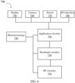
- FIG. 6 is a block diagram of an example system 700 for wireless communication according to an embodiment of the present disclosure. Embodiments described herein may be implemented into the system using any suitably configured hardware and/or software.
- FIG. 6 illustrates the system 700 including a radio frequency (RF) circuitry 710, a baseband circuitry 720, an application circuitry 730, a memory/storage 740, a display 750, a camera 760, a sensor 770, and an input/output (I/O) interface 780, coupled with each other at least as illustrated.
- the application circuitry 730 may include a circuitry such as, but not limited to, one or more single-core or multi-core processors.
- the processors may include any combination of general-purpose processors and dedicated processors, such as graphics processors, application processors.
- the processors may be coupled with the memory/storage and configured to execute instructions stored in the memory/storage to enable various applications and/or operating systems running on the system.
- the baseband circuitry 720 may include circuitry such as, but not limited to, one or more single-core or multi-core processors.
- the processors may include a baseband processor.
- the baseband circuitry may handle various radio control functions that enables communication with one or more radio networks via the RF circuitry.
- the radio control functions may include, but are not limited to, signal modulation, encoding, decoding, radio frequency shifting, etc.
- the baseband circuitry may provide for communication compatible with one or more radio technologies.
- the baseband circuitry may support communication with an evolved universal terrestrial radio access network (EUTRAN) and/or other wireless metropolitan area networks (WMAN), a wireless local area network (WLAN), a wireless personal area network (WPAN).
- EUTRAN evolved universal terrestrial radio access network
- WMAN wireless metropolitan area networks
- WLAN wireless local area network
- WPAN wireless personal area network
- Embodiments in which the baseband circuitry is configured to support radio communications of more than one wireless protocol may be referred to as multi-mode baseband circuit
- the baseband circuitry 720 may include circuitry to operate with signals that are not strictly considered as being in a baseband frequency.
- baseband circuitry may include circuitry to operate with signals having an intermediate frequency, which is between a baseband frequency and a radio frequency.
- the RF circuitry 710 may enable communication with wireless networks using modulated electromagnetic radiation through a non-solid medium.
- the RF circuitry may include switches, filters, amplifiers, etc. to facilitate the communication with the wireless network.
- the RF circuitry 710 may include circuitry to operate with signals that are not strictly considered as being in a radio frequency.
- RF circuitry may include circuitry to operate with signals having an intermediate frequency, which is between a baseband frequency and a radio frequency.
- the transmitter circuitry, control circuitry, or receiver circuitry discussed above with respect to the user equipment, eNB, or gNB may be embodied in whole or in part in one or more of the RF circuitry, the baseband circuitry, and/or the application circuitry.
- circuitry may refer to, be part of, or include an Application Specific Integrated Circuit (ASIC), an electronic circuit, a processor (shared, dedicated, or group), and/or a memory (shared, dedicated, or group) that execute one or more software or firmware programs, a combinational logic circuit, and/or other suitable hardware components that provide the described functionality.
- ASIC Application Specific Integrated Circuit
- the electronic device circuitry may be implemented in, or functions associated with the circuitry may be implemented by, one or more software or firmware modules.
- some or all of the constituent components of the baseband circuitry, the application circuitry, and/or the memory/storage may be implemented together on a system on a chip (SOC).
- SOC system on a chip
- the memory/storage 740 may be used to load and store data and/or instructions, for example, for system.
- the memory/storage for one embodiment may include any combination of suitable volatile memory, such as dynamic random access memory (DRAM)), and/or non-volatile memory, such as flash memory.
- DRAM dynamic random access memory
- flash memory non-volatile memory
- the I/O interface 780 may include one or more user interfaces designed to enable user interaction with the system and/or peripheral component interfaces designed to enable peripheral component interaction with the system.
- User interfaces may include, but are not limited to a physical keyboard or keypad, a touchpad, a speaker, a microphone, etc.
- Peripheral component interfaces may include, but are not limited to, a non-volatile memory port, a universal serial bus (USB) port, an audio jack, and a power supply interface.
- the sensor 770 may include one or more sensing devices to determine environmental states and/or location first information related to the system.
- the sensors may include, but are not limited to, a gyro sensor, an accelerometer, a proximity sensor, an ambient light sensor, and a positioning unit.
- the positioning unit may also be part of, or interact with, the baseband circuitry and/or RF circuitry to communicate with components of a positioning network, e.g., a global positioning system (GPS) satellite.
- GPS global positioning system
- the display 750 may include a display, such as a liquid crystal display and a touch screen display.
- the system 700 may be a mobile computing device such as, but not limited to, a laptop computing device, a tablet computing device, a netbook, an ultrabook, a smartphone, a AR/VR glasses, etc.
- system may have more or less components, and/or different architectures.
- methods described herein may be implemented as a computer program.
- the computer program may be stored on a storage medium, such as a non-transitory storage medium.
- the units as separating components for explanation are or are not physically separated.
- the units for display are or are not physical units, that is, located in one place or distributed on a plurality of network units. Some or all of the units are used according to the purposes of the embodiments.
- each of the functional units in each of the embodiments can be integrated in one processing unit, physically independent, or integrated in one processing unit with two or more than two units.
Landscapes
- Engineering & Computer Science (AREA)
- Signal Processing (AREA)
- Computer Networks & Wireless Communication (AREA)
- Quality & Reliability (AREA)
- Mobile Radio Communication Systems (AREA)
Claims (17)
- Procédé de traitement d'informations, comprenant les étapes consistant à :(402) déterminer, par un équipement d'utilisateur (10), une séquence de décalages cycliques comprenant N décalages cycliques selon des informations d'acquittement de demande de répétition automatique hybride (HARQ-ACK) à émettre et/ou une demande de programmation (SR) à émettre, une ressource dans un domaine fréquentiel utilisé pour émettre les informations HARQ-ACK à émettre et/ou la SR à émettre étant un entrelacement cible, l'entrelacement cible comprenant N blocs de ressources physiques (PRB), les N décalages cycliques étant en correspondance biunivoque avec les N PRB, et N étant un nombre entier supérieur à 1 ;(404) générer, par l'équipement d'utilisateur (10), un canal physique de commande en liaison montante (PUCCH) cible sur la base d'un format_0 de PUCCH selon la séquence de décalages cycliques ; et(406) émettre, par l'équipement d'utilisateur (10), le PUCCH cible sur l'entrelacement cible,le procédé étant caractérisé en ce que :la séquence de décalages cycliques est obtenue à partir d'une séquence de paramètres mcs , la séquence de paramètres mcs comprend N paramètres mcs , et les N décalages cycliques sont en correspondance biunivoque avec les N paramètres mcs ,un élément de départ de la séquence de paramètres mcs est

 des éléments adjacents dans la séquence de paramètres mcs sont fixés à intervalles égaux, une valeur de l'intervalle est T, et T est un nombre entier relativement premier par rapport à 12.
 - Procédé selon la revendication 1, dans lequel les N décalages cycliques sont en séquence de α 0 à α N-1 et les N PRB sont en séquence de PRB 0 à PRB N-1 ; et
la correspondance biunivoque entre les N décalages cycliques et les N PRB comprend : αi dans la séquence de décalages cycliques correspond à PRBi dans les N PRB, et une plage de valeurs de i est [0, N-1]. - Procédé selon la revendication 1, dans lequel les N paramètres mcs sont en séquence de


αi dans la séquence de décalages cycliques correspond à
- Procédé selon l'une quelconque des revendications 1 à 3, dans lequel :
la SR comprend l'une des SR suivantes : une SR négative ou une SR positive. - Procédé selon la revendication 1, dans lequel T est égal à 5,

- Procédé selon la revendication 1, dans lequel des valeurs distinctes de

- Procédé de traitement d'informations, comprenant les étapes consistant à :(502) analyser, par une station de base (20), un canal physique de commande en liaison montante (PUCCH) cible sur un entrelacement cible sur la base d'un format_0 de PUCCH selon une séquence de décalages cycliques comprenant N décalages cycliques ;(504) obtenir, par la station de base (20), un schéma de modulation et de codage (MCS)-0 en analysant la séquence de décalages cycliques ; et(506) obtenir, par la station de base (20), des informations d'acquittement de demande de répétition automatique hybride (HARQ-ACK) et/ou une demande de programmation (SR) sur le PUCCH, une ressource dans un domaine fréquentiel utilisé pour émettre les informations HARQ-ACK et/ou la SR étant l'entrelacement cible, l'entrelacement cible comprenant N blocs de ressources physiques (PRB), les N décalages cycliques étant en correspondance biunivoque avec les N PRB, et N étant un nombre entier supérieur à 1,le procédé étant caractérisé en ce que :la séquence de décalages cycliques est obtenue à partir d'une séquence de paramètres mcs , la séquence de paramètres mcs comprend N paramètres mcs , et les N décalages cycliques sont en correspondance biunivoque avec les N paramètres mcs ,un élément de départ de la séquence de paramètres mcs est

 des éléments adjacents dans la séquence de paramètres mcs sont fixés à intervalles égaux, une valeur de l'intervalle est T, et T est un nombre entier relativement premier par rapport à 12.
 - Procédé selon la revendication 7, dans lequel les N décalages cycliques sont en séquence de α 0 à α N-1 et les N PRB sont en séquence de PRB 0 à PRB N-1 ; et
la correspondance biunivoque entre les N décalages cycliques et les N PRB comprend : αi dans la séquence de décalages cycliques correspond à PRBi dans les N PRB, et une plage de valeurs de i est [0, N-1]. - Procédé selon la revendication 7, dans lequel les N paramètres mcs sont en séquence de


αi dans la séquence de décalages cycliques correspond à
- Procédé selon l'une quelconque des revendications 7 à 9, dans lequel :
la SR comprend l'une des SR suivantes : une SR négative ou une SR positive. - Procédé selon la revendication 7, dans lequel T est égal à 5,

- Procédé selon la revendication 7, dans lequel des valeurs distinctes de

- Équipement d'utilisateur (10), comprenant :une mémoire ;un émetteur-récepteur ; etun processeur couplé à la mémoire et à l'émetteur-récepteur ;le processeur étant configuré pour déterminer une séquence de décalages cycliques comprenant N décalages cycliques selon des informations d'acquittement de demande de répétition automatique hybride (HARQ-ACK) à émettre et/ou une demande de programmation (SR) à émettre, une ressource dans un domaine fréquentiel utilisé pour émettre les informations HARQ-ACK à émettre et/ou la SR à émettre étant un entrelacement cible, l'entrelacement cible comprenant N blocs de ressources physiques (PRB), les N décalages cycliques étant en correspondance biunivoque avec les N PRB, et N étant un nombre entier supérieur à 1 ;le processeur étant configuré pour générer un canal physique de commande en liaison montante (PUCCH) cible sur la base d'un format_0 de PUCCH selon la séquence de décalages cycliques ;l'émetteur-récepteur étant configuré pour émettre le PUCCH cible sur l'entrelacement cible,l'équipement d'utilisateur étant caractérisé en ce que :la séquence de décalages cycliques est obtenue à partir d'une séquence de paramètres mcs , la séquence de paramètres mcs comprend N paramètres mcs , et les N décalages cycliques sont en correspondance biunivoque avec les N paramètres mcs ;un élément de départ de la séquence de paramètres mcs est

 des éléments adjacents dans la séquence de paramètres mcs sont fixés à intervalles égaux, une valeur de l'intervalle est T, et T est un nombre entier relativement premier par rapport à 12.
 - Équipement d'utilisateur selon la revendication 13, dans lequel :lorsque les informations HARQ-ACK ont une longueur de 1 bit et une valeur de 0 ou lorsque la SR est une SR négative et que les informations HARQ-ACK ont une longueur de 1 bit et une valeur de 0, la valeur de
 lorsque les informations HARQ-ACK ont une longueur de 1 bit et une valeur de 1 ou lorsque la SR est la SR négative et que les informations HARQ-ACK ont une longueur de 1 bit et une valeur de 1, la valeur de
 ou dans lequel :lorsque les informations HARQ-ACK ont une longueur de 2 bits et une valeur de {0, 0} ou lorsque la SR est une SR négative et que les informations HARQ-ACK ont une longueur de 2 bits et une valeur de {0, 0}, la valeur de
 lorsque les informations HARQ-ACK ont une longueur de 2 bits et une valeur de {0, 1} ou lorsque la SR est la SR négative et que les informations HARQ-ACK ont une longueur de 2 bits et une valeur de {0, 1}, la valeur de
 lorsque les informations HARQ-ACK ont une longueur de 2 bits et une valeur de {1, 1} ou lorsque la SR est la SR négative et que les informations HARQ-ACK ont une longueur de 2 bits et une valeur de {1, 1}, la valeur de
 lorsque les informations HARQ-ACK ont une longueur de 2 bits et une valeur de {1, 0} ou lorsque la SR est la SR négative et que les informations HARQ-ACK ont une longueur de 2 bits et une valeur de {1, 0}, la valeur de
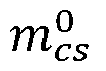
- Équipement d'utilisateur selon la revendication 13, dans lequel :lorsque la SR est une SR positive et que les informations HARQ-ACK ont une longueur de 1 bit et une valeur de 0, la valeur de
 lorsque la SR est la SR positive et que les informations HARQ-ACK ont une longueur de 1 bit et une valeur de 1, la valeur de
 ou dans lequel :lorsque la SR est une SR positive et que les informations HARQ-ACK ont une longueur de 2 bits et une valeur de {0, 0}, la valeur de
 lorsque la SR est la SR positive et que les informations HARQ-ACK ont une longueur de 2 bits et une valeur de {0, 1}, la valeur de
 lorsque la SR est la SR positive et que les informations HARQ-ACK ont une longueur de 2 bits et une valeur de {1, 1}, la valeur de
 lorsque la SR est la SR positive et que les informations HARQ-ACK ont une longueur de 2 bits et une valeur de {1, 0}, la valeur de
- Station de base (20), comprenant :une mémoire ;un émetteur-récepteur ; etun processeur couplé à la mémoire et à l'émetteur-récepteur ;le processeur étant configuré pour :analyser un canal physique de commande en liaison montante (PUCCH) cible sur un entrelacement cible sur la base d'un format_0 de PUCCH selon une séquence de décalages cycliques comprenant N décalages cycliques ;obtenir un schéma de modulation et de codage (MCS)-0 en analysant la séquence de décalages cycliques ; etobtenir des informations d'acquittement de demande de répétition automatique hybride (HARQ-ACK) et/ou une demande de programmation (SR) sur le PUCCH, une ressource dans un domaine fréquentiel utilisé pour émettre les informations HARQ-ACK et/ou la SR étant l'entrelacement cible, l'entrelacement cible comprenant N blocs de ressources physiques (PRB), les N décalages cycliques étant en correspondance biunivoque avec les N PRB, et N étant un nombre entier supérieur à 1,la station de base étant caractérisée en ce que :la séquence de décalages cycliques est obtenue à partir d'une séquence de paramètres mcs , la séquence de paramètres mcs comprend N paramètres mcs , et les N décalages cycliques sont en correspondance biunivoque avec les N paramètres mcs ,un élément de départ de la séquence de paramètres mcs est

 des éléments adjacents dans la séquence de paramètres mcs sont fixés à intervalles égaux, une valeur de l'intervalle est T, et T est un nombre entier relativement premier par rapport à 12.
 - Station de base selon la revendication 16, dans laquelle :lorsque les informations HARQ-ACK ont une longueur de 1 bit et une valeur de 0 ou lorsque la SR est une SR négative et que les informations HARQ-ACK ont une longueur de 1 bit et une valeur de 0, la valeur de
 lorsque les informations HARQ-ACK ont une longueur de 1 bit et une valeur de 1 ou lorsque la SR est la SR négative et que les informations HARQ-ACK ont une longueur de 1 bit et une valeur de 1, la valeur de
 ou dans lequel :lorsque les informations HARQ-ACK ont une longueur de 2 bits et une valeur de {0, 0} ou lorsque la SR est une SR négative et que les informations HARQ-ACK ont une longueur de 2 bits et une valeur de {0, 0}, la valeur de
 lorsque les informations HARQ-ACK ont une longueur de 2 bits et une valeur de {0, 1} ou lorsque la SR est la SR négative et que les informations HARQ-ACK ont une longueur de 2 bits et une valeur de {0, 1}, la valeur de
 lorsque les informations HARQ-ACK ont une longueur de 2 bits et une valeur de {1, 1} ou lorsque la SR est la SR négative et que les informations HARQ-ACK ont une longueur de 2 bits et une valeur de {1, 1}, la valeur de
 lorsque les informations HARQ-ACK ont une longueur de 2 bits et une valeur de {1, 0} ou lorsque la SR est la SR négative et que les informations HARQ-ACK ont une longueur de 2 bits et une valeur de {1, 0}, la valeur de
Applications Claiming Priority (2)
| Application Number | Priority Date | Filing Date | Title |
|---|---|---|---|
| US201962893461P | 2019-08-29 | 2019-08-29 | |
| PCT/CN2020/112259 WO2021037245A1 (fr) | 2019-08-29 | 2020-08-28 | Appareil et procédé de traitement d'informations |
Publications (3)
| Publication Number | Publication Date |
|---|---|
| EP4011017A1 EP4011017A1 (fr) | 2022-06-15 |
| EP4011017A4 EP4011017A4 (fr) | 2022-08-17 |
| EP4011017B1 true EP4011017B1 (fr) | 2025-02-26 |
Family
ID=74684260
Family Applications (1)
| Application Number | Title | Priority Date | Filing Date |
|---|---|---|---|
| EP20856331.2A Active EP4011017B1 (fr) | 2019-08-29 | 2020-08-28 | Appareil et procédé de traitement d'informations |
Country Status (4)
| Country | Link |
|---|---|
| US (1) | US12143982B2 (fr) |
| EP (1) | EP4011017B1 (fr) |
| CN (1) | CN113875179A (fr) |
| WO (1) | WO2021037245A1 (fr) |
Families Citing this family (3)
| Publication number | Priority date | Publication date | Assignee | Title |
|---|---|---|---|---|
| US11553509B2 (en) * | 2019-08-27 | 2023-01-10 | Mediatek Singapore Pte. Ltd. | Enhanced PUCCH format 0 and format 1 design for new radio unlicensed spectrum operation |
| WO2021226968A1 (fr) * | 2020-05-14 | 2021-11-18 | Apple Inc. | Transmission d'informations de commande de liaison montante dans des communications sans fil |
| US20230106447A1 (en) * | 2021-10-01 | 2023-04-06 | Qualcomm Incorporated | Cyclic shifts for multiple resource block physical uplink control channel communications |
Family Cites Families (11)
| Publication number | Priority date | Publication date | Assignee | Title |
|---|---|---|---|---|
| CN108370297B (zh) * | 2015-12-07 | 2021-03-09 | 瑞典爱立信有限公司 | 用于对未许可载波的上行链路控制信道配置的方法和装置 |
| EP3579512B1 (fr) * | 2017-02-02 | 2022-07-06 | Ntt Docomo, Inc. | Terminal d'utilisateur et procédé de communications sans fil |
| CN120263357A (zh) * | 2017-05-03 | 2025-07-04 | 交互数字专利控股公司 | Wtru以及由wtru实施的方法 |
| CN108988997B (zh) * | 2017-05-31 | 2021-04-02 | 株式会社Kt | 收发pucch时多路复用调度请求信息和harqack/nack信息的方法及装置 |
| KR102356054B1 (ko) * | 2017-08-11 | 2022-02-08 | 주식회사 윌러스표준기술연구소 | 무선 통신 시스템에서 상향링크 제어채널의 송수신 방법, 장치, 및 시스템 |
| US10750484B2 (en) * | 2017-11-22 | 2020-08-18 | Qualcomm Incorporated | Physical uplink control channel (PUCCH) configuration for new-radio-spectrum sharing (NR-SS) |
| KR102786925B1 (ko) * | 2018-01-10 | 2025-03-25 | 인터디지탈 패튼 홀딩스, 인크 | 짧은 물리적 업링크 제어 채널 구조 |
| EP4120599B1 (fr) * | 2018-02-14 | 2024-04-03 | LG Electronics Inc. | Procédé d'émission et de réception de signal de liaison montante entre un terminal et une station de base dans un système de communication sans fil pour prendre en charge une bande sans licence et appareil le prenant en charge |
| US11997042B2 (en) * | 2018-02-15 | 2024-05-28 | Sharp Kabushiki Kaisha | Simultaneous HARQ-ACK and SR transmission on NR PUCCH |
| KR20250141842A (ko) * | 2018-08-10 | 2025-09-29 | 주식회사 윌러스표준기술연구소 | 무선 통신 시스템의 물리 채널 및 신호 송수신 방법 및 이를 이용하는 장치 |
| US11974283B2 (en) * | 2021-03-19 | 2024-04-30 | Qualcomm Incorporated | Implicit uplink control channel resource allocation |
-
2020
- 2020-08-28 CN CN202080037788.7A patent/CN113875179A/zh active Pending
- 2020-08-28 EP EP20856331.2A patent/EP4011017B1/fr active Active
- 2020-08-28 WO PCT/CN2020/112259 patent/WO2021037245A1/fr not_active Ceased
-
2022
- 2022-02-24 US US17/679,938 patent/US12143982B2/en active Active
Also Published As
| Publication number | Publication date |
|---|---|
| US20220279548A1 (en) | 2022-09-01 |
| EP4011017A4 (fr) | 2022-08-17 |
| US12143982B2 (en) | 2024-11-12 |
| WO2021037245A1 (fr) | 2021-03-04 |
| EP4011017A1 (fr) | 2022-06-15 |
| CN113875179A (zh) | 2021-12-31 |
Similar Documents
| Publication | Publication Date | Title |
|---|---|---|
| US12395966B2 (en) | User equipment and method of resource transmission | |
| US12250701B2 (en) | User equipment and method for hybrid automatic repeat request reporting | |
| US9985764B2 (en) | Terminal device, base station device, communication method, and integrated circuit for processing demodulation reference signals | |
| US11121795B2 (en) | User equipment and method for transmitting synchronization signal block of same | |
| US12022485B2 (en) | Method and apparatus for receiving downlink control information in wireless communication system | |
| US12143982B2 (en) | Apparatus and information processing method | |
| EP4104595B1 (fr) | Appareil et procédé de communication sans fil | |
| KR20220068955A (ko) | 업 링크 제어 정보의 전송 방법 및 장치 | |
| US12069745B2 (en) | Method and apparatus for transmitting and receiving signal in wireless communication system | |
| EP4236475A2 (fr) | Appareil et procédé d'émission ou de réception de canal de diffusion de liaison latérale physique | |
| US12289738B2 (en) | Apparatus and method of communication of same | |
| US20230025005A1 (en) | Apparatus and method of wireless communication | |
| EP4059169B1 (fr) | Appareil et procédé de communication sans fil | |
| US11589374B2 (en) | Method and device for transmitting/receiving signal in wireless communication system | |
| EP3713134B1 (fr) | Procédé de transmission pucch, terminal, et dispositif côté réseau | |
| WO2021110109A1 (fr) | Appareil et procédé de communication sans fil | |
| EP4586725A1 (fr) | Procédé et appareil de transmission d'informations de commande, dispositif et support de stockage |
Legal Events
| Date | Code | Title | Description |
|---|---|---|---|
| STAA | Information on the status of an ep patent application or granted ep patent |
Free format text: STATUS: THE INTERNATIONAL PUBLICATION HAS BEEN MADE |
|
| PUAI | Public reference made under article 153(3) epc to a published international application that has entered the european phase |
Free format text: ORIGINAL CODE: 0009012 |
|
| STAA | Information on the status of an ep patent application or granted ep patent |
Free format text: STATUS: REQUEST FOR EXAMINATION WAS MADE |
|
| 17P | Request for examination filed |
Effective date: 20220307 |
|
| AK | Designated contracting states |
Kind code of ref document: A1 Designated state(s): AL AT BE BG CH CY CZ DE DK EE ES FI FR GB GR HR HU IE IS IT LI LT LU LV MC MK MT NL NO PL PT RO RS SE SI SK SM TR |
|
| A4 | Supplementary search report drawn up and despatched |
Effective date: 20220720 |
|
| RIC1 | Information provided on ipc code assigned before grant |
Ipc: H04W 72/04 20090101ALI20220714BHEP Ipc: H04L 1/18 20060101AFI20220714BHEP |
|
| DAV | Request for validation of the european patent (deleted) | ||
| DAX | Request for extension of the european patent (deleted) | ||
| GRAP | Despatch of communication of intention to grant a patent |
Free format text: ORIGINAL CODE: EPIDOSNIGR1 |
|
| STAA | Information on the status of an ep patent application or granted ep patent |
Free format text: STATUS: GRANT OF PATENT IS INTENDED |
|
| INTG | Intention to grant announced |
Effective date: 20241112 |
|
| GRAS | Grant fee paid |
Free format text: ORIGINAL CODE: EPIDOSNIGR3 |
|
| GRAA | (expected) grant |
Free format text: ORIGINAL CODE: 0009210 |
|
| STAA | Information on the status of an ep patent application or granted ep patent |
Free format text: STATUS: THE PATENT HAS BEEN GRANTED |
|
| AK | Designated contracting states |
Kind code of ref document: B1 Designated state(s): AL AT BE BG CH CY CZ DE DK EE ES FI FR GB GR HR HU IE IS IT LI LT LU LV MC MK MT NL NO PL PT RO RS SE SI SK SM TR |
|
| REG | Reference to a national code |
Ref country code: GB Ref legal event code: FG4D |
|
| REG | Reference to a national code |
Ref country code: CH Ref legal event code: EP |
|
| REG | Reference to a national code |
Ref country code: DE Ref legal event code: R096 Ref document number: 602020046947 Country of ref document: DE |
|
| REG | Reference to a national code |
Ref country code: IE Ref legal event code: FG4D |
|
| P01 | Opt-out of the competence of the unified patent court (upc) registered |
Free format text: CASE NUMBER: APP_9747/2025 Effective date: 20250226 |
|
| REG | Reference to a national code |
Ref country code: NL Ref legal event code: MP Effective date: 20250226 |
|
| PG25 | Lapsed in a contracting state [announced via postgrant information from national office to epo] |
Ref country code: RS Free format text: LAPSE BECAUSE OF FAILURE TO SUBMIT A TRANSLATION OF THE DESCRIPTION OR TO PAY THE FEE WITHIN THE PRESCRIBED TIME-LIMIT Effective date: 20250526 |
|
| PG25 | Lapsed in a contracting state [announced via postgrant information from national office to epo] |
Ref country code: FI Free format text: LAPSE BECAUSE OF FAILURE TO SUBMIT A TRANSLATION OF THE DESCRIPTION OR TO PAY THE FEE WITHIN THE PRESCRIBED TIME-LIMIT Effective date: 20250226 |
|
| PG25 | Lapsed in a contracting state [announced via postgrant information from national office to epo] |
Ref country code: PL Free format text: LAPSE BECAUSE OF FAILURE TO SUBMIT A TRANSLATION OF THE DESCRIPTION OR TO PAY THE FEE WITHIN THE PRESCRIBED TIME-LIMIT Effective date: 20250226 |
|
| PG25 | Lapsed in a contracting state [announced via postgrant information from national office to epo] |
Ref country code: ES Free format text: LAPSE BECAUSE OF FAILURE TO SUBMIT A TRANSLATION OF THE DESCRIPTION OR TO PAY THE FEE WITHIN THE PRESCRIBED TIME-LIMIT Effective date: 20250226 |
|
| REG | Reference to a national code |
Ref country code: LT Ref legal event code: MG9D |
|
| PG25 | Lapsed in a contracting state [announced via postgrant information from national office to epo] |
Ref country code: IS Free format text: LAPSE BECAUSE OF FAILURE TO SUBMIT A TRANSLATION OF THE DESCRIPTION OR TO PAY THE FEE WITHIN THE PRESCRIBED TIME-LIMIT Effective date: 20250626 Ref country code: NO Free format text: LAPSE BECAUSE OF FAILURE TO SUBMIT A TRANSLATION OF THE DESCRIPTION OR TO PAY THE FEE WITHIN THE PRESCRIBED TIME-LIMIT Effective date: 20250526 |
|
| PG25 | Lapsed in a contracting state [announced via postgrant information from national office to epo] |
Ref country code: NL Free format text: LAPSE BECAUSE OF FAILURE TO SUBMIT A TRANSLATION OF THE DESCRIPTION OR TO PAY THE FEE WITHIN THE PRESCRIBED TIME-LIMIT Effective date: 20250226 |
|
| PG25 | Lapsed in a contracting state [announced via postgrant information from national office to epo] |
Ref country code: HR Free format text: LAPSE BECAUSE OF FAILURE TO SUBMIT A TRANSLATION OF THE DESCRIPTION OR TO PAY THE FEE WITHIN THE PRESCRIBED TIME-LIMIT Effective date: 20250226 |
|
| PG25 | Lapsed in a contracting state [announced via postgrant information from national office to epo] |
Ref country code: PT Free format text: LAPSE BECAUSE OF FAILURE TO SUBMIT A TRANSLATION OF THE DESCRIPTION OR TO PAY THE FEE WITHIN THE PRESCRIBED TIME-LIMIT Effective date: 20250626 Ref country code: LV Free format text: LAPSE BECAUSE OF FAILURE TO SUBMIT A TRANSLATION OF THE DESCRIPTION OR TO PAY THE FEE WITHIN THE PRESCRIBED TIME-LIMIT Effective date: 20250226 |
|
| PG25 | Lapsed in a contracting state [announced via postgrant information from national office to epo] |
Ref country code: GR Free format text: LAPSE BECAUSE OF FAILURE TO SUBMIT A TRANSLATION OF THE DESCRIPTION OR TO PAY THE FEE WITHIN THE PRESCRIBED TIME-LIMIT Effective date: 20250527 Ref country code: BG Free format text: LAPSE BECAUSE OF FAILURE TO SUBMIT A TRANSLATION OF THE DESCRIPTION OR TO PAY THE FEE WITHIN THE PRESCRIBED TIME-LIMIT Effective date: 20250226 |
|
| REG | Reference to a national code |
Ref country code: AT Ref legal event code: MK05 Ref document number: 1771717 Country of ref document: AT Kind code of ref document: T Effective date: 20250226 |
|
| PG25 | Lapsed in a contracting state [announced via postgrant information from national office to epo] |
Ref country code: SE Free format text: LAPSE BECAUSE OF FAILURE TO SUBMIT A TRANSLATION OF THE DESCRIPTION OR TO PAY THE FEE WITHIN THE PRESCRIBED TIME-LIMIT Effective date: 20250226 |
|
| PG25 | Lapsed in a contracting state [announced via postgrant information from national office to epo] |
Ref country code: SM Free format text: LAPSE BECAUSE OF FAILURE TO SUBMIT A TRANSLATION OF THE DESCRIPTION OR TO PAY THE FEE WITHIN THE PRESCRIBED TIME-LIMIT Effective date: 20250226 |
|
| PG25 | Lapsed in a contracting state [announced via postgrant information from national office to epo] |
Ref country code: DK Free format text: LAPSE BECAUSE OF FAILURE TO SUBMIT A TRANSLATION OF THE DESCRIPTION OR TO PAY THE FEE WITHIN THE PRESCRIBED TIME-LIMIT Effective date: 20250226 |
|
| PGFP | Annual fee paid to national office [announced via postgrant information from national office to epo] |
Ref country code: DE Payment date: 20250819 Year of fee payment: 6 |
|
| PG25 | Lapsed in a contracting state [announced via postgrant information from national office to epo] |
Ref country code: IT Free format text: LAPSE BECAUSE OF FAILURE TO SUBMIT A TRANSLATION OF THE DESCRIPTION OR TO PAY THE FEE WITHIN THE PRESCRIBED TIME-LIMIT Effective date: 20250226 |
|
| PGFP | Annual fee paid to national office [announced via postgrant information from national office to epo] |
Ref country code: GB Payment date: 20250822 Year of fee payment: 6 |
|
| PG25 | Lapsed in a contracting state [announced via postgrant information from national office to epo] |
Ref country code: AT Free format text: LAPSE BECAUSE OF FAILURE TO SUBMIT A TRANSLATION OF THE DESCRIPTION OR TO PAY THE FEE WITHIN THE PRESCRIBED TIME-LIMIT Effective date: 20250226 |
|
| PGFP | Annual fee paid to national office [announced via postgrant information from national office to epo] |
Ref country code: FR Payment date: 20250818 Year of fee payment: 6 |
|
| PG25 | Lapsed in a contracting state [announced via postgrant information from national office to epo] |
Ref country code: EE Free format text: LAPSE BECAUSE OF FAILURE TO SUBMIT A TRANSLATION OF THE DESCRIPTION OR TO PAY THE FEE WITHIN THE PRESCRIBED TIME-LIMIT Effective date: 20250226 Ref country code: CZ Free format text: LAPSE BECAUSE OF FAILURE TO SUBMIT A TRANSLATION OF THE DESCRIPTION OR TO PAY THE FEE WITHIN THE PRESCRIBED TIME-LIMIT Effective date: 20250226 |
|
| PG25 | Lapsed in a contracting state [announced via postgrant information from national office to epo] |
Ref country code: RO Free format text: LAPSE BECAUSE OF FAILURE TO SUBMIT A TRANSLATION OF THE DESCRIPTION OR TO PAY THE FEE WITHIN THE PRESCRIBED TIME-LIMIT Effective date: 20250226 |
|
| PG25 | Lapsed in a contracting state [announced via postgrant information from national office to epo] |
Ref country code: SK Free format text: LAPSE BECAUSE OF FAILURE TO SUBMIT A TRANSLATION OF THE DESCRIPTION OR TO PAY THE FEE WITHIN THE PRESCRIBED TIME-LIMIT Effective date: 20250226 |
|
| REG | Reference to a national code |
Ref country code: DE Ref legal event code: R097 Ref document number: 602020046947 Country of ref document: DE |
|
| REG | Reference to a national code |
Ref country code: CH Ref legal event code: W10 Free format text: ST27 STATUS EVENT CODE: U-0-0-W10-W00 (AS PROVIDED BY THE NATIONAL OFFICE) Effective date: 20251217 |
|
| PLBE | No opposition filed within time limit |
Free format text: ORIGINAL CODE: 0009261 |
|
| STAA | Information on the status of an ep patent application or granted ep patent |
Free format text: STATUS: NO OPPOSITION FILED WITHIN TIME LIMIT |
|
| REG | Reference to a national code |
Ref country code: CH Ref legal event code: L10 Free format text: ST27 STATUS EVENT CODE: U-0-0-L10-L00 (AS PROVIDED BY THE NATIONAL OFFICE) Effective date: 20260107 |
|
| RAP2 | Party data changed (patent owner data changed or rights of a patent transferred) |
Owner name: ORIENTAL IP INVESTMENT LIMITED |
|
| 26N | No opposition filed |
Effective date: 20251127 |
|
| REG | Reference to a national code |
Ref country code: DE Ref legal event code: R081 Ref document number: 602020046947 Country of ref document: DE Owner name: ORIENTAL IP INVESTMENT LIMITED, HK Free format text: FORMER OWNER: GUANGDONG OPPO MOBILE TELECOMMUNICATIONS CORP., LTD., DONGGUAN, GUANGDONG, CN Ref country code: DE Ref legal event code: R082 Ref document number: 602020046947 Country of ref document: DE Representative=s name: BERGGREN PATENTANWAELTE PARTNERSCHAFT MBB, DE |
|
| REG | Reference to a national code |
Ref country code: GB Ref legal event code: 732E Free format text: REGISTERED BETWEEN 20260205 AND 20260211 |
|
| REG | Reference to a national code |
Ref country code: CH Ref legal event code: H13 Free format text: ST27 STATUS EVENT CODE: U-0-0-H10-H13 (AS PROVIDED BY THE NATIONAL OFFICE) Effective date: 20260324 |
|
| PG25 | Lapsed in a contracting state [announced via postgrant information from national office to epo] |
Ref country code: MC Free format text: LAPSE BECAUSE OF FAILURE TO SUBMIT A TRANSLATION OF THE DESCRIPTION OR TO PAY THE FEE WITHIN THE PRESCRIBED TIME-LIMIT Effective date: 20250226 |
|
| PG25 | Lapsed in a contracting state [announced via postgrant information from national office to epo] |
Ref country code: LU Free format text: LAPSE BECAUSE OF NON-PAYMENT OF DUE FEES Effective date: 20250828 |
|
| PG25 | Lapsed in a contracting state [announced via postgrant information from national office to epo] |
Ref country code: CH Free format text: LAPSE BECAUSE OF NON-PAYMENT OF DUE FEES Effective date: 20250831 |