EP4012431A1 - Élément magnétorésistif pour détecter un champ magnétique dans un axe z - Google Patents
Élément magnétorésistif pour détecter un champ magnétique dans un axe z Download PDFInfo
- Publication number
- EP4012431A1 EP4012431A1 EP20315489.3A EP20315489A EP4012431A1 EP 4012431 A1 EP4012431 A1 EP 4012431A1 EP 20315489 A EP20315489 A EP 20315489A EP 4012431 A1 EP4012431 A1 EP 4012431A1
- Authority
- EP
- European Patent Office
- Prior art keywords
- layer
- magnetoresistive element
- magnetization
- sense
- vortex
- Prior art date
- Legal status (The legal status is an assumption and is not a legal conclusion. Google has not performed a legal analysis and makes no representation as to the accuracy of the status listed.)
- Granted
Links
Images


Classifications
-
- G—PHYSICS
- G01—MEASURING; TESTING
- G01R—MEASURING ELECTRIC VARIABLES; MEASURING MAGNETIC VARIABLES
- G01R33/00—Arrangements or instruments for measuring magnetic variables
- G01R33/02—Measuring direction or magnitude of magnetic fields or magnetic flux
- G01R33/06—Measuring direction or magnitude of magnetic fields or magnetic flux using galvano-magnetic devices
- G01R33/09—Magnetoresistive devices
- G01R33/098—Magnetoresistive devices comprising tunnel junctions, e.g. tunnel magnetoresistance sensors
-
- H—ELECTRICITY
- H01—ELECTRIC ELEMENTS
- H01F—MAGNETS; INDUCTANCES; TRANSFORMERS; SELECTION OF MATERIALS FOR THEIR MAGNETIC PROPERTIES
- H01F10/00—Thin magnetic films, e.g. of one-domain structure
- H01F10/002—Antiferromagnetic thin films, i.e. films exhibiting a Néel transition temperature
-
- H—ELECTRICITY
- H01—ELECTRIC ELEMENTS
- H01F—MAGNETS; INDUCTANCES; TRANSFORMERS; SELECTION OF MATERIALS FOR THEIR MAGNETIC PROPERTIES
- H01F10/00—Thin magnetic films, e.g. of one-domain structure
- H01F10/08—Thin magnetic films, e.g. of one-domain structure characterised by magnetic layers
- H01F10/10—Thin magnetic films, e.g. of one-domain structure characterised by magnetic layers characterised by the composition
- H01F10/12—Thin magnetic films, e.g. of one-domain structure characterised by magnetic layers characterised by the composition being metals or alloys
- H01F10/14—Thin magnetic films, e.g. of one-domain structure characterised by magnetic layers characterised by the composition being metals or alloys containing iron or nickel
-
- H—ELECTRICITY
- H01—ELECTRIC ELEMENTS
- H01F—MAGNETS; INDUCTANCES; TRANSFORMERS; SELECTION OF MATERIALS FOR THEIR MAGNETIC PROPERTIES
- H01F10/00—Thin magnetic films, e.g. of one-domain structure
- H01F10/08—Thin magnetic films, e.g. of one-domain structure characterised by magnetic layers
- H01F10/10—Thin magnetic films, e.g. of one-domain structure characterised by magnetic layers characterised by the composition
- H01F10/12—Thin magnetic films, e.g. of one-domain structure characterised by magnetic layers characterised by the composition being metals or alloys
- H01F10/16—Thin magnetic films, e.g. of one-domain structure characterised by magnetic layers characterised by the composition being metals or alloys containing cobalt
-
- H—ELECTRICITY
- H01—ELECTRIC ELEMENTS
- H01F—MAGNETS; INDUCTANCES; TRANSFORMERS; SELECTION OF MATERIALS FOR THEIR MAGNETIC PROPERTIES
- H01F10/00—Thin magnetic films, e.g. of one-domain structure
- H01F10/32—Spin-exchange-coupled multilayers, e.g. nanostructured superlattices
- H01F10/324—Exchange coupling of magnetic film pairs via a very thin non-magnetic spacer, e.g. by exchange with conduction electrons of the spacer
- H01F10/3254—Exchange coupling of magnetic film pairs via a very thin non-magnetic spacer, e.g. by exchange with conduction electrons of the spacer the spacer being semiconducting or insulating, e.g. for spin tunnel junction [STJ]
-
- H—ELECTRICITY
- H01—ELECTRIC ELEMENTS
- H01F—MAGNETS; INDUCTANCES; TRANSFORMERS; SELECTION OF MATERIALS FOR THEIR MAGNETIC PROPERTIES
- H01F10/00—Thin magnetic films, e.g. of one-domain structure
- H01F10/32—Spin-exchange-coupled multilayers, e.g. nanostructured superlattices
- H01F10/324—Exchange coupling of magnetic film pairs via a very thin non-magnetic spacer, e.g. by exchange with conduction electrons of the spacer
- H01F10/3268—Exchange coupling of magnetic film pairs via a very thin non-magnetic spacer, e.g. by exchange with conduction electrons of the spacer the exchange coupling being asymmetric, e.g. by use of additional pinning, by using antiferromagnetic or ferromagnetic coupling interface, i.e. so-called spin-valve [SV] structure, e.g. NiFe/Cu/NiFe/FeMn
- H01F10/3272—Exchange coupling of magnetic film pairs via a very thin non-magnetic spacer, e.g. by exchange with conduction electrons of the spacer the exchange coupling being asymmetric, e.g. by use of additional pinning, by using antiferromagnetic or ferromagnetic coupling interface, i.e. so-called spin-valve [SV] structure, e.g. NiFe/Cu/NiFe/FeMn by use of anti-parallel coupled [APC] ferromagnetic layers, e.g. artificial ferrimagnets [AFI], artificial [AAF] or synthetic [SAF] anti-ferromagnets
-
- G—PHYSICS
- G01—MEASURING; TESTING
- G01R—MEASURING ELECTRIC VARIABLES; MEASURING MAGNETIC VARIABLES
- G01R33/00—Arrangements or instruments for measuring magnetic variables
- G01R33/02—Measuring direction or magnitude of magnetic fields or magnetic flux
- G01R33/0206—Three-component magnetometers
-
- H—ELECTRICITY
- H01—ELECTRIC ELEMENTS
- H01F—MAGNETS; INDUCTANCES; TRANSFORMERS; SELECTION OF MATERIALS FOR THEIR MAGNETIC PROPERTIES
- H01F10/00—Thin magnetic films, e.g. of one-domain structure
- H01F10/32—Spin-exchange-coupled multilayers, e.g. nanostructured superlattices
- H01F10/324—Exchange coupling of magnetic film pairs via a very thin non-magnetic spacer, e.g. by exchange with conduction electrons of the spacer
- H01F10/3286—Spin-exchange coupled multilayers having at least one layer with perpendicular magnetic anisotropy
Definitions
- the present invention concerns a magnetoresistive element comprising a sense layer, for measuring an external magnetic field along an axis substantially perpendicular to the plane of the sense layer.
- the present invention further concerns a method for operating the magnetoresistive element.
- One solution includes a separate single-axis planar magnetoresistive sensor installed perpendicular to a two-axis planar sensor. This solution requires assembling two different sensors, the X-Y two-axis magnetoresistive sensor and the Z-axis magnetoresistive sensor.
- Yet another solution includes micro-machining a substrate to form an inclined plane, onto which a sensor that partially senses the magnetic field in the Z-axis direction is deposited.
- Such a process is very complicated, has a low spatial efficiency, and may cause some shadowing effects in the deposition of the sensor, which may degrade the performance of the sensor.
- Yet another solution includes using magnetic materials with perpendicular magnetic anisotropy for measuring the magnetic field in the Z-axis direction.
- document US20130168787 discloses a magnetic sensor which measures a Z-axis component of an external magnetic field by using a perpendicular magnetic anisotropy material.
- the perpendicular magnetic anisotropy material has a high coercivity, and low magnetoresistance.
- the magnetoresistive element disclosed herein can measure an external magnetic field along an out-of-plane axis substantially perpendicular to the plane of the sense layer.
- the vortex configuration of the magnetoresistive element can have an expulsion field greater than 200 mT or 250 mT.
- the magnetoresistive element has low hysteresis, less than 300 ⁇ V/V for external magnetic field magnitudes up to the expulsion field, and high linearity, i.e., less than 2% or 1% error.
- Fig. 1 illustrates a magnetoresistive element 2, according to an embodiment,
- the magnetoresistive element comprises a reference layer 21 having a fixed reference magnetization 210, a sense layer 23 having a free sense magnetization 230 and a tunnel barrier layer 22 between the reference layer 21 and the sense layer 23.
- the sense magnetization 230 comprises a vortex configuration substantially parallel to the plane of the sense layer 23 in the absence of an external magnetic field 60.
- the reference layer 21 can have perpendicular magnetic anisotropy (PMA) such that the reference magnetization 210 is oriented substantially perpendicular to the plane of the reference layer 21.
- PMA perpendicular magnetic anisotropy
- the magnetoresistive element 2 can measure an external magnetic field 60 being oriented substantially perpendicular to the plane of the reference and sense layers 21, 23.
- the sense layer 23 has a sense magnetization 230 direction distribution with a vortex configuration, whereby the vortex magnetization curls in a circular path along the edge of the sense layer 23 and around a vortex core 231.
- the vortex magnetization direction may be arranged in a clockwise direction and may also be arranged in a counterclockwise direction.
- the magnetization of the vortex core 231 can vary in accordance to the external magnetic field 60 in a direction substantially perpendicular to the plane of the sense layer 23 (or direction ⁇ z). Referring to Fig. 1 , the magnetization of the vortex core 231 can be oriented in an upward direction (i.e., toward the direction +z) or in a downward direction (i.e., toward an opposite direction -z).
- the size of the vortex core increases or decreases in the direction +z or -z () when the magnitude of the external magnetic field 60 increases or decreases, respectively.
- the vortex core magnetization direction ⁇ z, or vortex core magnetization polarity is fixed.
- the vortex configuration provides a linear and non-hysteretic behavior in a large magnitude range of the external magnetic field 60, for practical size of the magnetoresistive element 2 and thickness of the sense layer 23.
- the linear and non-hysteretic portion of the magnetization curve facilitates the measurement of small variations of the external magnetic field 60.
- the vortex configuration is thus advantageous for magnetic sensor applications.
- Fig. 2 shows a magnetization curve (or hysteresis response) of the magnetoresistive element 2as a function of the external magnetic field 60 (indicated by the symbol B extz ).
- the magnetization curve is characterized by a linear increase of the vortex core magnetization with the external magnetic field B extz until the vortex expulsion field is reached at the H expl point.
- the sense magnetization 230 becomes magnetically saturated (represented by the arrow pointing upwards (the direction +z).
- the vortex state in the sensing layer 23 is recovered when the external magnetic field B extz is reduced below a nucleation field H nucl .
- the sense magnetization 230 becomes magnetically saturated (represented by the arrow pointing downwards (the direction -z).
- the nucleation field H nucl is the field at which vortex re-forms after vortex expulsion.
- the magnetization curve comprises a reversible linear portion corresponding to the variation of the vortex core 231 magnetization with the external magnetic field 60.
- the vortex core magnetization polarity can be reversed (between direction z and -z) when the expulsion field H expl is exceeded.
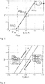
- Fig. 3 shows an enlarged view of a portion of the reversible linear portion of the magnetization curve of Fig. 2 .
- the magnetization curve to the external magnetic field B extz is shifted towards higher magnetization values when the external magnetic field B extz is decreased from the nucleation field H nucl , compared to when the external magnetic field B extz is increased from the nucleation field H nucl .
- the reversible linear portion of the magnetization curve exhibits a hysteresis due to the different vortex core magnetization polarity, that is the direction of the vortex core 231 magnetization.
- the vortex core magnetization polarity depends on the nucleation field +/-H nucl at which the vortex re-forms after vortex expulsion. It is then possible to operate the magnetoresistive element 2 in only one of the branch of the magnetization curve, for example the branch A (see Fig. 3 ) when the field is swept back to negative from the positive nucleation field +H nucl (and the positive vortex expulsion field +H expl ) or the branch B when the field is swept back to positive from the negative nucleation field - H nucl (and the negative vortex expulsion field -H expl ).
- a method for operating the magnetoresistive element 2 can comprise the steps of selecting the direction z or -z of the vortex core magnetization (vortex core magnetization polarity) by applying an initialization magnetic field to the magnetoresistive element 2 until the vortex expulsion field H expl is reached and then, reducing the initialization magnetic field below the nucleation field H nucl at which the vortex re-forms.
- the vortex core magnetization polarity is determined by the polarity of the vortex expulsion field H expl and the nucleation field H nucl .
- the method further comprises the step of measuring an external magnetic field 60.
- the method can further comprise a step of programming the magnetoresistive element 2 to program the orientation of the reference magnetization 210.
- the programming step can be performed by applying a programming magnetic field adapted to orient the reference magnetization 210.
- the programming step can further comprise heating the magnetoresistive element 2 to a temperature where the orientation of the reference magnetization 210 is facilitated, for example at a temperature where the reference magnetization 210 is unpinned. Heating the magnetoresistive element 2 can be performed by using resistive heating or laser heating.
- the vortex core magnetization polarity can be considered fixed.
- the operation of the magnetoresistive element 2 is not limited to any specific portion of the branches A or B shown in Fig. 3 . Indeed, the magnetoresistive element 2 can be operated anywhere in the linear region of branch A or branch B (the latter with a vortex magnetization polarity reversed relative to the one in branch A).
- the magnetoresistive element 2 should measure the external magnetic field 60 below the vortex expulsion field +/-H expl .
- the vortex magnetization polarity is fixed during sensor operation and is independent of vortex chirality (clockwise or counterclockwise).
- Fig. 4 reports magnetization curves to the z-aligned external magnetic field B extz on the magnetization of the sense layer 23, for several thickness of the sense layer 23, namely for thicknesses of the sense layer 23 between 10 nm and 60 nm.
- the magnetoresistive element 2 has a lateral dimension D of about 250 nm.
- Fig. 4 shows an increase in the slope of the magnetization curve, and thus the susceptibility ⁇ , with increasing thickness of the sense layer 23. For a given TMR value, increasing the thicknesses of the sense layer 23 results in an increase of the sensitivity S of the magnetoresistive element 2. This is in contrast to the case of a vortex configuration in the the plane of the sense layer 23 and having a vortex core magnetization that is reversibly movable substantially parallel to the plane of the sense layer 23.
- Fig. 5 reports magnetization curves to the z-aligned external magnetic field B extz of the sense layer 23 for several thickness of the sense layer 23, namely for thicknesses of the sense layer 23 between 10 nm and 60 nm.
- the magnetoresistive element 2 has a lateral dimension of about 450 nm.
- Figs. 4 and 5 show that the susceptibility ⁇ increases, and for a given TMR value the sensitivity S of the magnetoresistive element 2 increases, with decreasing smaller lateral dimension D of the magnetoresistive element 2. For given thicknesses of the layers 21, 23, the value the sensitivity S increases with increasing the aspect ratio t/D of the thickness t to the diameter (lateral dimension) D of the magnetoresistive element 2.
- the sensitivity S of the magnetoresistive element 2 is plotted as a function of the thickness of the sense layer 23 in Fig. 6 .
- the sensitivity S was simulated for lateral dimensions D of the magnetoresistive element 2 of 150 nm, 200 nm and 250 nm, and for magnetizations of the sense layer 23 of 400 and 600 kA/m.
- the TMR value of the magnetoresistive element 2 was assumed to be 100%.
- Fig. 6 shows that the higher values of sensitivity S are obtained for a lateral dimension of 150 nm and a magnetization of 400 kA/m.
- decreasing the sense magnetization 230 of the sense layer 23 results in an increase of the sensitivity S of the magnetoresistive element 2.
- the expression "sense magnetization” is used indifferently for "saturation sense magnetization” or “spontaneous sense magnetization", where saturation magnetization has its usual meaning of the maximum induced magnetic moment.
- the results shown above suggest providing the magnetoresistive element 2 where the reference layer 21 has a reference magnetization 210 oriented substantially perpendicular to the plane of the reference layer 21, and where the sense layer 23 has a sense magnetization 230 comprising a vortex configuration in the absence of an external magnetic field 60.
- the vortex configuration should be substantially parallel to the plane of the sense layer 23 and have a vortex core 231 magnetization along an out-of-plane axis 50 substantially perpendicular to the plane of the sense layer 23.
- the magnetoresistive element 2 should have small lateral dimension D (or high aspect ratio), for example a lateral dimension D below 300 nm, preferably below 250 nm, or preferably below 150 nm, and a small sense magnetization 230 of the sense layer 23, for example a sense magnetization below 850 kA/m, possibly below 600 kA/m or possibly below 400 kA/M.
- the sense layer 23 has a thickness of that is greater than 50 nm or preferably greater than 100 nm.
- the thickness of the sense layer 23 can be thick (more than 50 nm) and the sense magnetization 230 of the sense layer 23 can have value that is corresponds to typical saturation magnetization values found in conventional magnetoresistive elements (for example 600 kA/m or larger).
- the magnetoresistive element 2 has a lateral dimension D of 250 nm and the sense layer 23 has a thickness of 110 nm.
- the ferromagnetic material forming the sense layer 23 can comprise a ferromagnetic alloy having a sense magnetization of 600 kA/m or larger (here 600 kA/m).
- the low sense magnetization of the sense layer 23 can be obtained by decreasing the thickness (for example below 50 nm) and/or by a proper selection of the ferromagnetic material forming the sense layer 23 such as to obtain a low sense magnetization (for example lower than 600 kA/m).
- the magnetoresistive element 2 has a lateral dimension D of 250 nm
- the sense layer 23 has a thickness of 46 nm and has a sense magnetization of 400 kA/m.
- the sense layer 23 can be formed a ferromagnetic alloy having a low magnetization.
- Figs. 7 and 8 show that a substantially identical magnetization curve is obtained for the magnetoresistive element 2 of the first and second examples.
- the expulsion field H expl can be about 300 mT and the nucleation field H nucl can be about 200 mT.
- the reference layer 21 can comprise a synthetic antiferromagnetic (SAF) structure including a first reference sublayer 211 in contact with the tunnel barrier layer 22 and a second reference sublayer 212 separated from the first reference sublayer 211 by a coupling layer 213, wherein the coupling layer 213 antiferromagnetically couple the first reference sublayer 211 to the second reference sublayer 212.
- SAF synthetic antiferromagnetic
- Each of the first and second reference sublayer 211, 212 has PMA such that a reference magnetization 210 is oriented substantially perpendicular to the plane of the first and second reference sublayer 211, 212 and in opposite directions.
- each of the first and second reference sublayer 211, 212 includes a multilayer structure.
- each of the first and second reference sublayer 211, 212 can include a plurality of alternating first metallic layers 201 and second metallic layers 202.
- the first metallic layer 201 can comprise an ultrathin Co layer and the second metallic layer 202 can comprise an ultrathin Pt layer.
- the second metallic layer 202 preferably comprises Pt, other metals that provide PMA can also be used.
- the ultrathin Co layer 201 can have a thickness between 0.4 nm and 0.6 nm.
- the ultrathin Pt layer 202 can have a thickness between 0.2 nm and 0.4 nm.
- the coupling layer 213 can be a Ru layer. Although the coupling layer 213 preferably comprises Ru, other metals that generate RKKY coupling can also be used.
- the reference layer 21 comprising the SAF structure according to the configuration of Fig. 9 can achieve a field stability of greater than 300 mT to 400 mT.
Landscapes
- Engineering & Computer Science (AREA)
- Power Engineering (AREA)
- Physics & Mathematics (AREA)
- Chemical & Material Sciences (AREA)
- Crystallography & Structural Chemistry (AREA)
- Condensed Matter Physics & Semiconductors (AREA)
- General Physics & Mathematics (AREA)
- Hall/Mr Elements (AREA)
- Measuring Magnetic Variables (AREA)
Priority Applications (5)
| Application Number | Priority Date | Filing Date | Title |
|---|---|---|---|
| EP20315489.3A EP4012431B1 (fr) | 2020-12-11 | 2020-12-11 | Élément magnétorésistif pour détecter un champ magnétique dans un axe z |
| PCT/IB2021/061484 WO2022123472A1 (fr) | 2020-12-11 | 2021-12-09 | Élément magnétorésistif pour la détection d'un champ magnétique selon un axe z |
| JP2023535328A JP2023553931A (ja) | 2020-12-11 | 2021-12-09 | Z軸線の磁場を検知する磁気抵抗素子 |
| US18/256,494 US12320873B2 (en) | 2020-12-11 | 2021-12-09 | Magnetoresistive element for sensing a magnetic field in a Z-axis |
| KR1020237019328A KR20230117352A (ko) | 2020-12-11 | 2021-12-09 | Z축의 자기장을 감지하기 위한 자기 저항 요소 |
Applications Claiming Priority (1)
| Application Number | Priority Date | Filing Date | Title |
|---|---|---|---|
| EP20315489.3A EP4012431B1 (fr) | 2020-12-11 | 2020-12-11 | Élément magnétorésistif pour détecter un champ magnétique dans un axe z |
Publications (3)
| Publication Number | Publication Date |
|---|---|
| EP4012431A1 true EP4012431A1 (fr) | 2022-06-15 |
| EP4012431C0 EP4012431C0 (fr) | 2025-07-02 |
| EP4012431B1 EP4012431B1 (fr) | 2025-07-02 |
Family
ID=74187108
Family Applications (1)
| Application Number | Title | Priority Date | Filing Date |
|---|---|---|---|
| EP20315489.3A Active EP4012431B1 (fr) | 2020-12-11 | 2020-12-11 | Élément magnétorésistif pour détecter un champ magnétique dans un axe z |
Country Status (5)
| Country | Link |
|---|---|
| US (1) | US12320873B2 (fr) |
| EP (1) | EP4012431B1 (fr) |
| JP (1) | JP2023553931A (fr) |
| KR (1) | KR20230117352A (fr) |
| WO (1) | WO2022123472A1 (fr) |
Cited By (2)
| Publication number | Priority date | Publication date | Assignee | Title |
|---|---|---|---|---|
| EP4257998A1 (fr) * | 2022-04-05 | 2023-10-11 | Commissariat à l'énergie atomique et aux énergies alternatives | Capteur magnétorésistif sensible à un champ magnétique hors plan |
| EP4417989A1 (fr) | 2023-02-17 | 2024-08-21 | Allegro MicroSystems, LLC | Elément magnétorésistif à axe de sensibilité hors plan et à hystérésis réduite et à plage de champ de travail augmentée |
Families Citing this family (2)
| Publication number | Priority date | Publication date | Assignee | Title |
|---|---|---|---|---|
| EP4012431B1 (fr) | 2020-12-11 | 2025-07-02 | Allegro MicroSystems, LLC | Élément magnétorésistif pour détecter un champ magnétique dans un axe z |
| US20250372300A1 (en) | 2024-05-31 | 2025-12-04 | Allegro Microsystems, Llc | Perpendicular MR SAF |
Citations (5)
| Publication number | Priority date | Publication date | Assignee | Title |
|---|---|---|---|---|
| US20110102939A1 (en) * | 2008-07-14 | 2011-05-05 | Fuji Electric Holdings Co., Ltd. | Spin valve element, method of driving the same, and storage device using the same |
| US20120206137A1 (en) | 2011-02-14 | 2012-08-16 | Memsic, Inc. | Monolithic tri-axis amr sensor and manufacturing method thereof |
| US20130168787A1 (en) | 2011-12-28 | 2013-07-04 | Industrial Technology Research Institute | Magnetic sensor |
| WO2013180277A1 (fr) * | 2012-05-31 | 2013-12-05 | 国立大学法人九州大学 | Oscillateur |
| EP3726237A2 (fr) * | 2019-04-18 | 2020-10-21 | Nxp B.V. | Capteur de champ magnétique, système et procédé de mesure de la vitesse |
Family Cites Families (32)
| Publication number | Priority date | Publication date | Assignee | Title |
|---|---|---|---|---|
| JP2002374019A (ja) * | 2001-06-15 | 2002-12-26 | Oki Noboru | 双安定メモリ要素及び磁気メモリ |
| JP2003198003A (ja) * | 2001-12-27 | 2003-07-11 | Sony Corp | 磁気抵抗効果素子およびその製造方法並びに磁気メモリ装置 |
| EP1934984B1 (fr) | 2005-09-30 | 2011-05-18 | Nxp B.V. | Memoire vive magnetique a nanofils |
| US7697243B1 (en) * | 2006-09-08 | 2010-04-13 | The United States Of America As Represented By The United States Department Of Energy | Method for the detection of a magnetic field utilizing a magnetic vortex |
| JP4232808B2 (ja) * | 2006-09-19 | 2009-03-04 | 日立金属株式会社 | 磁気エンコーダ装置 |
| FR2924851B1 (fr) | 2007-12-05 | 2009-11-20 | Commissariat Energie Atomique | Element magnetique a ecriture assistee thermiquement. |
| JP5170679B2 (ja) * | 2008-01-29 | 2013-03-27 | 日立金属株式会社 | 磁気センサおよび回転角度検出装置 |
| US20100320550A1 (en) * | 2009-06-23 | 2010-12-23 | International Business Machines Corporation | Spin-Torque Magnetoresistive Structures with Bilayer Free Layer |
| US8273582B2 (en) | 2009-07-09 | 2012-09-25 | Crocus Technologies | Method for use in making electronic devices having thin-film magnetic components |
| EP2479759A1 (fr) | 2011-01-19 | 2012-07-25 | Crocus Technology S.A. | Cellule magnétique de mémoire à accès aléatoire faible puissance |
| EP2546836A1 (fr) | 2011-07-12 | 2013-01-16 | Crocus Technology S.A. | Cellule magnétique de mémoire à accès aléatoire dotée d'une dispersion améliorée du champ de commutation |
| EP2712078B1 (fr) | 2012-09-25 | 2015-06-03 | Crocus Technology S.A. | Cellule d'unité logique magnétique (MLU) et amplificateur possédant un signal magnétique linéaire |
| EP2712079B1 (fr) | 2012-09-25 | 2015-06-03 | Crocus Technology S.A. | Cellule à unité logique magnétique (MLU) et amplificateur possédant un signal magnétique linéaire |
| US10989769B2 (en) * | 2013-12-27 | 2021-04-27 | Infineon Technologies Ag | Magneto-resistive structured device having spontaneously generated in-plane closed flux magnetization pattern |
| US20150200355A1 (en) | 2014-01-15 | 2015-07-16 | Allegro Microsystems, Llc | Fabricating a via |
| DE102015121753B4 (de) * | 2015-12-14 | 2021-10-21 | Infineon Technologies Ag | Magnetsensorbauelement und Verfahren für ein Magnetsensorbauelement mit einer magnetoresistiven Struktur |
| US20170330070A1 (en) * | 2016-02-28 | 2017-11-16 | Purdue Research Foundation | Spin orbit torque based electronic neuron |
| US10593869B2 (en) | 2016-07-26 | 2020-03-17 | Allegro Microsystems, Llc | Methods for patterning a magnetic sensing layer |
| US10050193B1 (en) | 2017-06-05 | 2018-08-14 | Allegro Microsystems, Llc | Magnetoresistance structure patterning |
| US10605874B2 (en) | 2018-08-06 | 2020-03-31 | Allegro Microsystems, Llc | Magnetic field sensor with magnetoresistance elements having varying sensitivity |
| EP3667346B1 (fr) | 2018-12-11 | 2022-06-08 | Crocus Technology S.A. | Dispositif de capteur angulaire magnétique pour détecter des champs magnétiques élevés ayant une faible erreur angulaire |
| JP7136340B2 (ja) * | 2019-04-09 | 2022-09-13 | 株式会社村田製作所 | 磁気抵抗素子および磁気センサ |
| EP3731230B1 (fr) | 2019-04-23 | 2024-06-26 | Allegro MicroSystems, LLC | Élément magnétique doté d'une meilleure plage de mesure |
| EP3761050A1 (fr) | 2019-07-02 | 2021-01-06 | Crocus Technology S.A. | Capteur de champ magnétique pour détecter un champ magnétique externe bidimensionnel ayant un champ anisotrope faible |
| EP3761043B1 (fr) | 2019-07-05 | 2023-09-06 | Crocus Technology SA | Capteur de courant magnétique comprenant un pont complet différentiel magnétorésistif |
| EP4012431B1 (fr) | 2020-12-11 | 2025-07-02 | Allegro MicroSystems, LLC | Élément magnétorésistif pour détecter un champ magnétique dans un axe z |
| EP4308947B1 (fr) | 2021-03-19 | 2025-11-26 | Allegro MicroSystems, LLC | Élément magnétorésistif et dispositif capteur magnétique ayant une sensibilité élevée et un décalage de champ nul faible |
| US12442874B2 (en) | 2021-11-04 | 2025-10-14 | Allegro Microsystems, Llc | Angle sensor with a single die using a single target |
| US11719527B2 (en) | 2021-11-04 | 2023-08-08 | Allegro Microsystems, Llc | Angle sensor with a single die using a single target |
| US12310246B2 (en) | 2022-05-31 | 2025-05-20 | Allegro Microsystems, Llc | Fabricating an electroconductive contact on a top surface of a tunneling magnetoresistance element |
| US12130342B2 (en) | 2022-06-10 | 2024-10-29 | Allegro Microsystems, Llc | Magnetic field current sensor to reduce stray magnetic fields |
| US12364163B2 (en) | 2022-08-30 | 2025-07-15 | Allegro Microsystems, Llc | Fabricating an electroconductive contact on a top layer of a tunneling magnetoresistance element using two hard masks |
-
2020
- 2020-12-11 EP EP20315489.3A patent/EP4012431B1/fr active Active
-
2021
- 2021-12-09 WO PCT/IB2021/061484 patent/WO2022123472A1/fr not_active Ceased
- 2021-12-09 KR KR1020237019328A patent/KR20230117352A/ko active Pending
- 2021-12-09 US US18/256,494 patent/US12320873B2/en active Active
- 2021-12-09 JP JP2023535328A patent/JP2023553931A/ja active Pending
Patent Citations (5)
| Publication number | Priority date | Publication date | Assignee | Title |
|---|---|---|---|---|
| US20110102939A1 (en) * | 2008-07-14 | 2011-05-05 | Fuji Electric Holdings Co., Ltd. | Spin valve element, method of driving the same, and storage device using the same |
| US20120206137A1 (en) | 2011-02-14 | 2012-08-16 | Memsic, Inc. | Monolithic tri-axis amr sensor and manufacturing method thereof |
| US20130168787A1 (en) | 2011-12-28 | 2013-07-04 | Industrial Technology Research Institute | Magnetic sensor |
| WO2013180277A1 (fr) * | 2012-05-31 | 2013-12-05 | 国立大学法人九州大学 | Oscillateur |
| EP3726237A2 (fr) * | 2019-04-18 | 2020-10-21 | Nxp B.V. | Capteur de champ magnétique, système et procédé de mesure de la vitesse |
Non-Patent Citations (1)
| Title |
|---|
| RAHMAN N ET AL: "Thickness dependence of magnetization dynamics of an in-plane anisotropy ferromagnet under a crossed spin torque polarizer", JOURNAL OF MAGNETISM AND MAGNETIC MATERIALS, ELSEVIER, AMSTERDAM, NL, vol. 439, 8 May 2017 (2017-05-08), pages 95 - 100, XP085050054, ISSN: 0304-8853, DOI: 10.1016/J.JMMM.2017.05.016 * |
Cited By (4)
| Publication number | Priority date | Publication date | Assignee | Title |
|---|---|---|---|---|
| EP4257998A1 (fr) * | 2022-04-05 | 2023-10-11 | Commissariat à l'énergie atomique et aux énergies alternatives | Capteur magnétorésistif sensible à un champ magnétique hors plan |
| WO2023194346A1 (fr) * | 2022-04-05 | 2023-10-12 | Commissariat A L'energie Atomique Et Aux Energies Alternatives | Capteur magnétorésistif sensible à un champ magnétique hors plan |
| EP4417989A1 (fr) | 2023-02-17 | 2024-08-21 | Allegro MicroSystems, LLC | Elément magnétorésistif à axe de sensibilité hors plan et à hystérésis réduite et à plage de champ de travail augmentée |
| WO2024171048A1 (fr) | 2023-02-17 | 2024-08-22 | Allegro Microsystems, Llc | Élément magnétorésistif ayant un axe de sensibilité hors plan et ayant une hystérésis réduite et une plage de champ de travail accrue |
Also Published As
| Publication number | Publication date |
|---|---|
| WO2022123472A1 (fr) | 2022-06-16 |
| KR20230117352A (ko) | 2023-08-08 |
| EP4012431C0 (fr) | 2025-07-02 |
| JP2023553931A (ja) | 2023-12-26 |
| EP4012431B1 (fr) | 2025-07-02 |
| US20240027551A1 (en) | 2024-01-25 |
| US12320873B2 (en) | 2025-06-03 |
Similar Documents
| Publication | Publication Date | Title |
|---|---|---|
| EP4012431B1 (fr) | Élément magnétorésistif pour détecter un champ magnétique dans un axe z | |
| US9069033B2 (en) | 3-axis magnetic field sensor, method for fabricating magnetic field sensing structure and magnetic field sensing circuit | |
| EP3223028B1 (fr) | Capteur magnétique à axes multiples | |
| EP3229035B1 (fr) | Capteur de champ magnétique avec polarisation d'aimant permanent | |
| EP3208626B1 (fr) | Capteur de champ magnétique avec magnétisation de détection incline de couche de détection | |
| US12265139B2 (en) | Magneto-resistive element and magnetic sensor | |
| Ota et al. | CoFeB/MgO-based magnetic tunnel junction directly formed on a flexible substrate | |
| TW201327956A (zh) | 磁感應器 | |
| EP3236276B1 (fr) | Capteur de champ magnétique avec une capacité de détection à axes multiples | |
| US10254305B2 (en) | Inertial sensor | |
| Zhao et al. | L 10-MnGa based magnetic tunnel junction for high magnetic field sensor | |
| CN114937736A (zh) | 一种宽量程tmr传感器隧道结及传感器 | |
| WO2015129235A1 (fr) | Capteur magnétique | |
| US20240310461A1 (en) | Magnetoresistive sensor having a shielding element with vortex magnetization | |
| CN102360683B (zh) | 一种用于磁敏探头磁芯的复合材料 | |
| JP2015212628A (ja) | 磁気センサの使用方法及び磁気センサのバイアス磁場の決定方法 | |
| CN100442076C (zh) | 线性磁场传感器及其制作方法 | |
| CN104459574B (zh) | 一种磁传感装置的制备工艺 | |
| Ji et al. | Novel modeling and dynamic simulation of magnetic tunnel junctions for spintronic sensor development | |
| US20260029492A1 (en) | Tmr sensor with sensing multilayer structure | |
| CN104793150A (zh) | 一种磁传感器及该磁传感器的制备方法 | |
| US11921172B2 (en) | Magnetoresistive sensor element with synthetic antiferromagnet biasing | |
| Jiang et al. | A Method of Forming Full-Wheatstone Bridge for Linear TMR Magnetic Sensors | |
| JP2006019484A (ja) | 磁気センサ | |
| CN117518045A (zh) | 适于多温况对交变磁场快速响应的隧穿磁电阻磁敏传感器 |
Legal Events
| Date | Code | Title | Description |
|---|---|---|---|
| PUAI | Public reference made under article 153(3) epc to a published international application that has entered the european phase |
Free format text: ORIGINAL CODE: 0009012 |
|
| STAA | Information on the status of an ep patent application or granted ep patent |
Free format text: STATUS: THE APPLICATION HAS BEEN PUBLISHED |
|
| AK | Designated contracting states |
Kind code of ref document: A1 Designated state(s): AL AT BE BG CH CY CZ DE DK EE ES FI FR GB GR HR HU IE IS IT LI LT LU LV MC MK MT NL NO PL PT RO RS SE SI SK SM TR |
|
| STAA | Information on the status of an ep patent application or granted ep patent |
Free format text: STATUS: REQUEST FOR EXAMINATION WAS MADE |
|
| 17P | Request for examination filed |
Effective date: 20221108 |
|
| RBV | Designated contracting states (corrected) |
Designated state(s): AL AT BE BG CH CY CZ DE DK EE ES FI FR GB GR HR HU IE IS IT LI LT LU LV MC MK MT NL NO PL PT RO RS SE SI SK SM TR |
|
| RAP3 | Party data changed (applicant data changed or rights of an application transferred) |
Owner name: CROCUS TECHNOLOGY SA |
|
| RAP1 | Party data changed (applicant data changed or rights of an application transferred) |
Owner name: ALLEGRO MICROSYSTEMS, LLC |
|
| RAP1 | Party data changed (applicant data changed or rights of an application transferred) |
Owner name: ALLEGRO MICROSYSTEMS, LLC |
|
| GRAP | Despatch of communication of intention to grant a patent |
Free format text: ORIGINAL CODE: EPIDOSNIGR1 |
|
| STAA | Information on the status of an ep patent application or granted ep patent |
Free format text: STATUS: GRANT OF PATENT IS INTENDED |
|
| RIC1 | Information provided on ipc code assigned before grant |
Ipc: G01R 33/02 20060101ALN20250219BHEP Ipc: H01F 10/32 20060101ALI20250219BHEP Ipc: G01R 33/09 20060101AFI20250219BHEP |
|
| INTG | Intention to grant announced |
Effective date: 20250306 |
|
| GRAS | Grant fee paid |
Free format text: ORIGINAL CODE: EPIDOSNIGR3 |
|
| GRAA | (expected) grant |
Free format text: ORIGINAL CODE: 0009210 |
|
| STAA | Information on the status of an ep patent application or granted ep patent |
Free format text: STATUS: THE PATENT HAS BEEN GRANTED |
|
| AK | Designated contracting states |
Kind code of ref document: B1 Designated state(s): AL AT BE BG CH CY CZ DE DK EE ES FI FR GB GR HR HU IE IS IT LI LT LU LV MC MK MT NL NO PL PT RO RS SE SI SK SM TR |
|
| REG | Reference to a national code |
Ref country code: GB Ref legal event code: FG4D |
|
| REG | Reference to a national code |
Ref country code: CH Ref legal event code: EP |
|
| REG | Reference to a national code |
Ref country code: DE Ref legal event code: R096 Ref document number: 602020053728 Country of ref document: DE |
|
| REG | Reference to a national code |
Ref country code: IE Ref legal event code: FG4D |
|
| U01 | Request for unitary effect filed |
Effective date: 20250729 |
|
| U07 | Unitary effect registered |
Designated state(s): AT BE BG DE DK EE FI FR IT LT LU LV MT NL PT RO SE SI Effective date: 20250805 |
|
| U20 | Renewal fee for the european patent with unitary effect paid |
Year of fee payment: 6 Effective date: 20251110 |
|
| PG25 | Lapsed in a contracting state [announced via postgrant information from national office to epo] |
Ref country code: IS Free format text: LAPSE BECAUSE OF FAILURE TO SUBMIT A TRANSLATION OF THE DESCRIPTION OR TO PAY THE FEE WITHIN THE PRESCRIBED TIME-LIMIT Effective date: 20251102 |
|
| PG25 | Lapsed in a contracting state [announced via postgrant information from national office to epo] |
Ref country code: NO Free format text: LAPSE BECAUSE OF FAILURE TO SUBMIT A TRANSLATION OF THE DESCRIPTION OR TO PAY THE FEE WITHIN THE PRESCRIBED TIME-LIMIT Effective date: 20251002 |
|
| PG25 | Lapsed in a contracting state [announced via postgrant information from national office to epo] |
Ref country code: HR Free format text: LAPSE BECAUSE OF FAILURE TO SUBMIT A TRANSLATION OF THE DESCRIPTION OR TO PAY THE FEE WITHIN THE PRESCRIBED TIME-LIMIT Effective date: 20250702 |
|
| PG25 | Lapsed in a contracting state [announced via postgrant information from national office to epo] |
Ref country code: GR Free format text: LAPSE BECAUSE OF FAILURE TO SUBMIT A TRANSLATION OF THE DESCRIPTION OR TO PAY THE FEE WITHIN THE PRESCRIBED TIME-LIMIT Effective date: 20251003 |
|
| PG25 | Lapsed in a contracting state [announced via postgrant information from national office to epo] |
Ref country code: CZ Free format text: LAPSE BECAUSE OF FAILURE TO SUBMIT A TRANSLATION OF THE DESCRIPTION OR TO PAY THE FEE WITHIN THE PRESCRIBED TIME-LIMIT Effective date: 20250702 |
|
| PG25 | Lapsed in a contracting state [announced via postgrant information from national office to epo] |
Ref country code: PL Free format text: LAPSE BECAUSE OF FAILURE TO SUBMIT A TRANSLATION OF THE DESCRIPTION OR TO PAY THE FEE WITHIN THE PRESCRIBED TIME-LIMIT Effective date: 20250702 |
|
| PG25 | Lapsed in a contracting state [announced via postgrant information from national office to epo] |
Ref country code: RS Free format text: LAPSE BECAUSE OF FAILURE TO SUBMIT A TRANSLATION OF THE DESCRIPTION OR TO PAY THE FEE WITHIN THE PRESCRIBED TIME-LIMIT Effective date: 20251002 |
|
| PG25 | Lapsed in a contracting state [announced via postgrant information from national office to epo] |
Ref country code: ES Free format text: LAPSE BECAUSE OF FAILURE TO SUBMIT A TRANSLATION OF THE DESCRIPTION OR TO PAY THE FEE WITHIN THE PRESCRIBED TIME-LIMIT Effective date: 20250702 |
|
| PG25 | Lapsed in a contracting state [announced via postgrant information from national office to epo] |
Ref country code: SM Free format text: LAPSE BECAUSE OF FAILURE TO SUBMIT A TRANSLATION OF THE DESCRIPTION OR TO PAY THE FEE WITHIN THE PRESCRIBED TIME-LIMIT Effective date: 20250702 |
|
| PG25 | Lapsed in a contracting state [announced via postgrant information from national office to epo] |
Ref country code: SK Free format text: LAPSE BECAUSE OF FAILURE TO SUBMIT A TRANSLATION OF THE DESCRIPTION OR TO PAY THE FEE WITHIN THE PRESCRIBED TIME-LIMIT Effective date: 20250702 |