EP4012776B1 - Substrat d'affichage et son procédé de fabrication, panneau d'affichage et dispositif d'affichage - Google Patents
Substrat d'affichage et son procédé de fabrication, panneau d'affichage et dispositif d'affichage Download PDFInfo
- Publication number
- EP4012776B1 EP4012776B1 EP20904258.9A EP20904258A EP4012776B1 EP 4012776 B1 EP4012776 B1 EP 4012776B1 EP 20904258 A EP20904258 A EP 20904258A EP 4012776 B1 EP4012776 B1 EP 4012776B1
- Authority
- EP
- European Patent Office
- Prior art keywords
- base substrate
- trace
- power trace
- layer
- orthographic projection
- Prior art date
- Legal status (The legal status is an assumption and is not a legal conclusion. Google has not performed a legal analysis and makes no representation as to the accuracy of the status listed.)
- Active
Links
Images





Classifications
-
- H—ELECTRICITY
- H10—SEMICONDUCTOR DEVICES; ELECTRIC SOLID-STATE DEVICES NOT OTHERWISE PROVIDED FOR
- H10K—ORGANIC ELECTRIC SOLID-STATE DEVICES
- H10K59/00—Integrated devices, or assemblies of multiple devices, comprising at least one organic light-emitting element covered by group H10K50/00
- H10K59/10—OLED displays
- H10K59/12—Active-matrix OLED [AMOLED] displays
- H10K59/131—Interconnections, e.g. wiring lines or terminals
-
- H—ELECTRICITY
- H10—SEMICONDUCTOR DEVICES; ELECTRIC SOLID-STATE DEVICES NOT OTHERWISE PROVIDED FOR
- H10K—ORGANIC ELECTRIC SOLID-STATE DEVICES
- H10K50/00—Organic light-emitting devices
- H10K50/80—Constructional details
- H10K50/84—Passivation; Containers; Encapsulations
- H10K50/842—Containers
- H10K50/8426—Peripheral sealing arrangements, e.g. adhesives, sealants
-
- H—ELECTRICITY
- H10—SEMICONDUCTOR DEVICES; ELECTRIC SOLID-STATE DEVICES NOT OTHERWISE PROVIDED FOR
- H10K—ORGANIC ELECTRIC SOLID-STATE DEVICES
- H10K59/00—Integrated devices, or assemblies of multiple devices, comprising at least one organic light-emitting element covered by group H10K50/00
- H10K59/10—OLED displays
- H10K59/12—Active-matrix OLED [AMOLED] displays
- H10K59/121—Active-matrix OLED [AMOLED] displays characterised by the geometry or disposition of pixel elements
-
- H—ELECTRICITY
- H10—SEMICONDUCTOR DEVICES; ELECTRIC SOLID-STATE DEVICES NOT OTHERWISE PROVIDED FOR
- H10K—ORGANIC ELECTRIC SOLID-STATE DEVICES
- H10K59/00—Integrated devices, or assemblies of multiple devices, comprising at least one organic light-emitting element covered by group H10K50/00
- H10K59/10—OLED displays
- H10K59/12—Active-matrix OLED [AMOLED] displays
- H10K59/122—Pixel-defining structures or layers, e.g. banks
-
- H—ELECTRICITY
- H10—SEMICONDUCTOR DEVICES; ELECTRIC SOLID-STATE DEVICES NOT OTHERWISE PROVIDED FOR
- H10K—ORGANIC ELECTRIC SOLID-STATE DEVICES
- H10K59/00—Integrated devices, or assemblies of multiple devices, comprising at least one organic light-emitting element covered by group H10K50/00
- H10K59/10—OLED displays
- H10K59/12—Active-matrix OLED [AMOLED] displays
- H10K59/124—Insulating layers formed between TFT elements and OLED elements
-
- H—ELECTRICITY
- H10—SEMICONDUCTOR DEVICES; ELECTRIC SOLID-STATE DEVICES NOT OTHERWISE PROVIDED FOR
- H10K—ORGANIC ELECTRIC SOLID-STATE DEVICES
- H10K59/00—Integrated devices, or assemblies of multiple devices, comprising at least one organic light-emitting element covered by group H10K50/00
- H10K59/80—Constructional details
- H10K59/87—Passivation; Containers; Encapsulations
- H10K59/871—Self-supporting sealing arrangements
- H10K59/8722—Peripheral sealing arrangements, e.g. adhesives, sealants
-
- H—ELECTRICITY
- H10—SEMICONDUCTOR DEVICES; ELECTRIC SOLID-STATE DEVICES NOT OTHERWISE PROVIDED FOR
- H10K—ORGANIC ELECTRIC SOLID-STATE DEVICES
- H10K71/00—Manufacture or treatment specially adapted for the organic devices covered by this subclass
-
- H—ELECTRICITY
- H10—SEMICONDUCTOR DEVICES; ELECTRIC SOLID-STATE DEVICES NOT OTHERWISE PROVIDED FOR
- H10K—ORGANIC ELECTRIC SOLID-STATE DEVICES
- H10K59/00—Integrated devices, or assemblies of multiple devices, comprising at least one organic light-emitting element covered by group H10K50/00
- H10K59/10—OLED displays
- H10K59/12—Active-matrix OLED [AMOLED] displays
- H10K59/1201—Manufacture or treatment
Definitions
- the present disclosure relates to the field of display technology, and in particular to a display substrate and a manufacturing method thereof, a display panel, and a display device.
- Organic light emitting diode (OLED) display device is a self-luminous device and does not require a backlight. Compared with traditional liquid crystal display (LCD) devices, the OLED display device also provides more vivid colors and a larger color gamut. In addition, the OLED display devices may be made more flexible, thinner and lighter than typical LCD devices.
- the OLED display device generally includes an anode, an organic layer including an organic light-emitting layer, and a cathode.
- the OLED may be a bottom emission OLED or a top emission OLED. In the bottom emission OLED, light is extracted from an anode side. In the bottom emission OLED, the anode is usually transparent, and the cathode is usually reflective.
- top emission OLED In the top emission OLED, light is extracted from a cathode side.
- the cathode In the top emission OLED, the cathode is optically transparent, and the anode is reflective.
- the top emission OLED is more suitable for a high PPI display product, which adapts to market development trends and conforms to industry development trends. Therefore, designs of the top emission OLED display device have gradually become one of focuses of researchers.
- EP 1 895 592 A1 discloses an organic light emitting display device capable of hermetically sealing a space between a deposition substrate and an encapsulation substrate with inorganic sealing materials is disclosed.
- the organic light emitting display device includes a first substrate including power supply lines formed on an array, and a circumference of the array, of organic light emitting diodes, and connected to a pad unit through the power pad line to supply a power source to each of the organic light emitting diodes; a second substrate arranged on at least the array of the first substrate; and an inorganic sealing material for sealing an inner space between the first substrate and the second substrate while forming a closed boundary, where the inorganic sealing material is not overlapped with a region in which the power supply line is formed.
- US 2019/189730 A1 discloses a display substrate, including: a display region and a non-display region around the display region, where the non-display region of the display substrate includes: a gate driving circuit and a signal line on a base substrate, where the gate driving circuit is electrically insulated from the signal line, and an orthographic projection of the gate driving circuit onto the base substrate at least partially overlaps with an orthographic projection of the signal line onto the base substrate.
- the present disclosure provides a display substrate as defined in claim 1, and a manufacturing method of a display substrate as defined in claim 13.
- a display substrate including: a base substrate including a display area and a peripheral area located on at least a first side of the display area; a plurality of pixel units arranged in an array in a first direction and a second direction in the display area of the base substrate, wherein each of the pixel units includes a pixel drive circuit and a light-emitting device electrically connected to the pixel drive circuit, the light-emitting device includes a first electrode, a second electrode, and a light-emitting layer arranged between the first electrode and the second electrode; a first power trace located in the peripheral area and electrically connected to the first electrode; a second power trace located in the peripheral area and electrically connected to the second electrode; a planarization layer with at least a portion thereof being located in the peripheral area; and a frame sealant, wherein the peripheral area includes a first peripheral area located on a side of the frame sealant close to the display area and a second peripheral area located on a side of the frame sealant away from the display
- the planarization layer includes a first portion located in the first peripheral area and a second portion located in the second peripheral area, an orthographic projection of the first portion of the planarization layer on the base substrate at least partially overlaps the orthographic projection of each of the first power trace and the second power trace on the base substrate, and the first portion of the planarization layer is located between the first power trace and the second power trace.
- the display substrate further includes a plurality of pads arranged on the signal input side and located in the peripheral area, wherein the second portion of the planarization layer is adjacent to the plurality of pads, and is located on a side of the plurality of pads close to the frame sealant.
- the first portion of the planarization layer has a first side surface away from the display area
- the first power trace has a first side surface away from the display area
- the second power trace has a first side surface away from the display area
- the first side surface of the first power trace is farther away from the display area than the first side surface of the second power trace
- the first side surface of the first portion of the planarization layer is farther away from the display area than the first side surface of the first power trace.
- the first portion of the planarization layer is located on a side of the second power trace away from the base substrate and is in contact with a surface of the second power trace away from the base substrate.
- the first portion of the planarization layer is located on a side of the first power trace close to the base substrate and is in contact with a surface of the first power trace close to the base substrate.
- the display substrate further includes a first signal trace electrically connecting at least one of the plurality of pads and at least one of the plurality of pixel units, the first signal trace includes a first portion located in the first peripheral area and a second portion located in the second peripheral area, the first portion of the first signal trace is located in a different layer from the first power trace, the first portion of the planarization layer is located between the first power trace and the first portion of the first signal trace, and the orthographic projection of the first portion of the planarization layer on the base substrate at least partially overlaps an orthographic projection of the first portion of the first signal trace on the base substrate.
- an orthographic projection of the second portion of the planarization layer on the base substrate at least partially overlaps an orthographic projection of the second portion of the first signal trace on the base substrate.
- each of the first portion of the planarization layer and the second portion of the planarization layer is spaced apart from the frame sealant.
- each of the first portion of the planarization layer and the second portion of the planarization layer is spaced apart from the frame sealant by a distance above 50 microns.
- the display substrate further includes a second signal trace electrically connecting at least one of the plurality of pads and at least one of the plurality of pixel units, and the orthographic projection of the first power trace on the base substrate does not overlap an orthographic projection of the second signal trace on the base substrate.
- the first power trace includes a first portion and a second portion, an orthographic projection of the first portion of the first power trace on the base substrate at least partially overlaps the orthographic projection of the second power trace on the base substrate, and an orthographic projection of the second portion of the first power trace on the base substrate does not overlap the orthographic projection of the second power trace on the base substrate.
- the first portion of the first power trace has a first size in the first direction
- the second portion of the first power trace has a second size in the first direction
- the first size is greater than the second size
- the display substrate further includes: at least one thin film transistor arranged on the base substrate, wherein the thin film transistor includes an active layer, a gate electrode, a source electrode and a drain electrode; a first conductive layer arranged on a side of the active layer away from the base substrate, wherein the gate electrode is located in the first conductive layer; a second conductive layer arranged on a side of the first conductive layer away from the base substrate, wherein the source electrode and the drain electrode are located in the second conductive layer; a third conductive layer arranged on a side of the second conductive layer away from the base substrate, wherein the second electrode is located in the third conductive layer; and a fourth conductive layer arranged on a side of the third conductive layer away from the base substrate, wherein the first electrode is located in the fourth conductive layer.
- the display substrate further includes a passivation layer arranged between the second conductive layer and the third conductive layer, and the planarization layer is arranged between the passivation layer and the third conductive layer.
- the first power trace is located in the third conductive layer; and/or the second power trace is located in the first conductive layer.
- the display substrate further includes an auxiliary electrode trace located in the second conductive layer, wherein the auxiliary electrode trace electrically connects the first power trace and the first electrode.
- the display substrate further includes a first power lead located in the first conductive layer or the second conductive layer and a conductive connection portion located in the third conductive layer; the first power lead has one end connected to one of the plurality of pads and the other end connected to the first power trace through a first opening; and the first power trace is connected to the auxiliary electrode trace through a second opening, the auxiliary electrode trace is connected to the conductive connection portion through a third opening, and the conductive connection portion is connected to the first electrode through a fourth opening.
- the first power trace includes a first trace portion, a second trace portion and a third trace portion
- an orthographic projection of the second trace portion of the first power trace on the base substrate covers an orthographic projection of the first opening on the base substrate
- an orthographic projection of the third trace portion of the first power trace on the base substrate covers an orthographic projection of the second opening on the base substrate
- the first trace portion of the first power trace is a portion of the first power trace other than the second trace portion and the third trace portion
- the orthographic projection of the planarization layer on the base substrate covers an orthographic projection of the first trace portion of the first power trace on the base substrate.
- the display substrate further includes a pixel defining layer arranged on a side of the second electrode away from the base substrate, an orthographic projection of the pixel defining layer on the base substrate covers the orthographic projection of the first portion of the planarization layer on the base substrate.
- the pixel defining layer includes a first side surface away from the display area, and an orthographic projection of the first side surface of the pixel defining layer on the base substrate is farther away from the display area than an orthographic projection of the first side surface of the first portion of the planarization layer on the base substrate.
- the first electrode is a cathode of an organic light-emitting device
- the second electrode is an anode of the organic light-emitting device
- the cathode contains a transparent conductive material
- the anode contains a metal material
- the first signal trace includes a data trace for transmitting a data signal
- the second signal trace includes a scanning trace for transmitting a scanning signal
- connection When an element is described as being “on”, “connected to” or “coupled to” another element, the element may be directly on the other element, directly connected to the other element, or directly coupled to the other element, or an intermediate element may be present. However, when an element is described as being “directly on”, “directly connected to” or “directly coupled to” another element, no intermediate element is present. Other terms and/or expressions used to describe the relationship between elements, for example, “between” and “directly between”, “adjacent” and “directly adjacent”, “above” and “directly above”, and so on, should be interpreted in a similar manner.
- the term “connected” may refer to a physical connection, an electrical connection, a communication connection, and/or a fluid connection.
- X axis, Y axis and Z axis are not limited to three axes of a rectangular coordinate system, and may be interpreted in a broader meaning.
- the X axis, Y axis and Z axis may be perpendicular to each other, or may represent different directions that are not perpendicular to each other.
- "at least one of X, Y and Z" and "at least one selected from a group consisting of X, Y and Z” may be interpreted as only X, only Y, only Z, or any combination of two or more of X, Y and Z, such as XYZ, XYY, YZ and ZZ.
- the term "and/or" includes any and all combinations of one or more of listed related items.
- first a first component, a first member, a first element, a first region, a first layer and/or a first portion discussed below may be referred to as a second component, a second member, a second element, a second region, a second layer and/or a second portion without departing from the teachings of the present disclosure.
- spatial relationship terms such as “upper”, “lower”, “left”, “right”, may be used herein to describe the relationship between one element or feature and another element or feature as shown in the drawings. It should be understood that the spatial relationship terms are intended to cover other different orientations of the device in use or operation in addition to the orientation described in the figure. For example, if the device in the drawings is turned upside down, an element or feature described as “below” or “under” another element or feature will be oriented “above” or “on” the other element or feature.
- the expression “height” or “thickness” refers to a size in a direction perpendicular to a surface of each film layer arranged in the display panel, that is, a size in a light-emitting direction of the display panel, or called a size in a normal direction of the display device, or called a size in the Z direction in the drawings.
- patterning process generally includes steps of photoresist coating, exposure, development, etching, and photoresist stripping.
- one-time patterning process means a process of forming patterned layers, components elements and so on using one mask.
- the expressions “same layer”, “disposed in the same layer” or similar expressions refer to a layer structure formed by first using the same film forming process to form a film layer for forming a specific pattern, and then using the same mask to pattern the film layer by using one-time patterning process.
- the one-time patterning process may include multiple exposure, development or etching processes, and the specific patterns in the layer structure formed may be continuous or discontinuous. These specific patterns may also be at different heights or have different thicknesses.
- the expression “electrically connected” may mean that two components or elements are directly electrically connected.
- component or element A is in direct contact with component or element B, and electrical signals may be transmitted between the two components or elements. It may also mean that two components or elements are electrically connected through a conductive medium such as a conductive wire.
- component or element A is electrically connected to component or element B through a conductive wire so as to transmit electrical signals between the two components or elements.
- two components or elements are electrically connected through at least one electronic component.
- component or element A is electrically connected to component or element B through at least one thin film transistor so as to transmit electrical signals between the two components or elements.
- Embodiments of the present disclosure at least provide a display substrate, including: a base substrate including a display area and a peripheral area located on at least a first side of the display area; a plurality of pixel units arranged in an array in a first direction and a second direction in the display area of the base substrate, wherein each of the pixel units includes a pixel drive circuit and a light-emitting device electrically connected to the pixel drive circuit, the light-emitting device includes a first electrode, a second electrode, and a light-emitting layer arranged between the first electrode and the second electrode; a first power trace located in the peripheral area and electrically connected to the first electrode; a second power trace located in the peripheral area and electrically connected to the second electrode; a planarization layer with at least a portion thereof being located in the peripheral area; and a frame sealant, wherein the peripheral area includes a first peripheral area located on a side of the frame sealant close to the display area and a second peripheral area located on a side of the frame
- FIG. 1 shows a plan view of an OLED display panel according to some exemplary embodiments of the present disclosure.
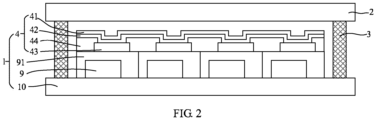
- FIG. 2 shows a cross-sectional view of the OLED display panel according to some exemplary embodiments of the present disclosure, taken along line AA' in FIG. 1 .
- the OLED display panel includes a first substrate 1 and a second substrate 2 opposite to the first substrate 1.
- the first substrate 1 may be an array substrate
- the second substrate 2 may be a cover plate formed of, for example, glass.
- the OLED display panel further includes a frame sealant 3 disposed between the first substrate 1 and the second substrate 2.
- the frame sealant 3 is arranged in a ring shape in a peripheral area of the first substrate 1, that is, a ring of frame sealant 3 is arranged in the peripheral area of the first substrate 1.
- the frame sealant 3 may prevent an intrusion of water vapor and oxygen, maintain a cell thickness of the peripheral area of the display panel, and bond the first substrate and the second substrate.
- a gap between the first substrate and the second substrate may also be filled with a filler, and the filler may be made of resin materials.
- a packaging structure of Dam&Filler is achieved. It should be noted that the embodiments of the present disclosure are not limited to this packaging structure, and other types of packaging structures may be used in the embodiments of the present disclosure without conflict.
- the first substrate 1 includes a base substrate 10.
- the base substrate 10 may be formed of glass, plastic, polyimide, or other materials.
- the base substrate 10 includes a display area AA and a peripheral area (or referred to as a non-display area) NA located on at least one side of the display area AA (for convenience of description, this side is referred to as a first side).
- the peripheral area NA includes a first peripheral area NA1 located on a side of the frame sealant 3 close to the display area AA and a second peripheral area NA2 located on a side of the frame sealant 3 away from the display area AA.
- the first substrate 1 includes a plurality of pixel units P (schematically shown by a dashed box in FIG. 1 ) arranged in the display area AA.
- the plurality of pixel units P is arranged in an array in a first direction X and a second direction Y on the base substrate 10.
- Each of the pixel units P may further include a plurality of sub-pixels, such as red sub-pixels, green sub-pixels and blue sub-pixels.
- a sub-pixel SP is schematically shown.
- the display panel includes a signal input side IN (the lower side shown in FIG. 1 ).
- a plurality of pads 7 are provided on the signal input side IN.
- the plurality of pads 7 may be electrically connected to the pixel units P located in the display area through a plurality of signal traces, and drive circuits may be electrically connected to the plurality of pads 7.
- signals such as data signals may be transmitted from the signal input side IN to the plurality of pixel units P.
- the above-mentioned first side may be the signal input side IN. That is, the peripheral area NA is located on at least the signal input side IN of the display area AA.
- the peripheral area NA may be located on four sides of the display area AA, that is, it surrounds the display area AA.
- the pixel units and sub-pixels are schematically shown in rectangular shapes, but this does not constitute a limitation on the shapes of the pixel units and sub-pixels included in the display panel provided by the embodiments of the present disclosure.
- the first substrate 1 further includes a light emitting device, such as an OLED device 4.
- a light emitting device such as an OLED device 4.
- the OLED device 4 includes a first electrode 41, a second electrode 43 opposite to the first electrode 41, and a light emitting layer 42 between the first electrode 41 and the second electrode 43.
- the first electrode 41 and the second electrode 43 is an anode, and the other one is a cathode.
- the first electrode 41 may be a transparent cathode, for example, it may be formed of a transparent conductive material, which may include indium tin oxide (ITO), indium zinc oxide (IZO), and the like.
- the second electrode 43 may be a reflective anode, for example, it may be formed of a metal material, which may include alloys such as magnesium aluminum alloy (MgAl), lithium aluminum alloy (LiAl), or single metals such as magnesium, aluminum and lithium.
- the light emitting layer 42 may have a multilayer structure, for example, it may include a multilayer structure including a hole injection layer, a hole transport layer, an organic light emitting layer, an electron transport layer and an electron injection layer.
- the OLED device 4 may adopt active drive or passive drive.
- the passive drive OLED array substrate includes a cathode and an anode, an intersection of the anode and the cathode may emit light, and the drive circuit may be externally mounted by a connection method such as a tape carrier package or chip-on-glass.
- the active drive OLED array substrate may be equipped with a pixel drive circuit for each pixel.
- the pixel drive circuit may include a thin film transistor with a switching function (that is, a switching transistor), a thin film transistor with a driving function (that is, a driving transistor), and a charge storage capacitor.
- the pixel drive circuit may further include other types of thin film transistors with compensation functions. It should be understood that, in the embodiments of the present disclosure, the display panel may be equipped with various types of known pixel drive circuits, which will not be repeated here.
- the first substrate 1 includes a drive circuit layer 9.
- the above-mentioned pixel drive circuit may be arranged in the drive circuit layer 9.
- An insulating layer 91 may be provided between the drive circuit layer 9 and the OLED device 4.
- the insulating layer 91 may be a single insulating film layer or a stacked layer including a plurality of insulating film layers.
- the first substrate 1 may further include various signal lines provided on the base substrate 10.
- the various signal lines include scanning lines, data lines, ELVDD power lines, ELVSS power lines and so on, so as to provide various signals such as control signals, data signals and power supply voltages to the pixel drive circuit in each sub-pixel.
- a scanning line GL and a data line DL are schematically shown.
- the scanning line GL and the data line DL may be electrically connected to each sub-pixel.
- FIG. 3 shows a partial plan view of the display panel according to some exemplary embodiments of the present disclosure on the signal input side.
- FIG. 4 shows a schematic exploded view of three film layers included in the display panel according to some exemplary embodiments of the present disclosure.
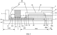
- FIG. 5 shows a cross-sectional view of a first substrate included in the display panel according to some exemplary embodiments of the present disclosure, taken along line BB' in FIG. 3 .
- FIG. 6 shows a cross-sectional view of the first substrate included in the display panel according to some exemplary embodiments of the present disclosure, taken along line CC' in FIG. 1 .
- FIG. 7 shows a cross-sectional view of the first substrate included in the display panel according to some exemplary embodiments of the present disclosure, taken along line DD' in FIG. 3 .
- the first substrate 1 includes a first power trace 5, a second power trace 6, a scanning trace GL', a data trace DL' and a plurality of pads 7 arranged on the base substrate 10.
- the first power trace 5, the second power trace 6, the scanning trace GL', the data trace DL' and the plurality of pads 7 are located in the peripheral area NA, for example, on the signal input side of the peripheral area NA, which is usually a bottom border of the display panel.
- an area where the plurality of pads 7 are located is referred to as a pad area 105, which is usually located on the signal input side of the peripheral area NA, as shown in FIG. 1 .
- the first power trace 5 may be a trace for providing a VSS voltage signal
- the second power trace 6 may be a trace for providing a VDD voltage signal.
- the first power trace 5 is electrically connected to the first electrode 41
- the second power trace 6 is electrically connected to the second electrode 43.
- “the second power trace 6 is electrically connected to the second electrode 43” here may mean that the second power trace 6 is electrically connected to the second electrode 43 through an electronic component such as the thin film transistor in the pixel drive circuit.
- the scanning trace GL' may have one end connected to the scanning line GL located in the display area AA and the other end connected to some pads 7.
- the data trace DL' may have one end connected to the data line DL located in the display area AA and the other end connected to the other pads 7.
- the plurality of pads 7 may be connected to a driver such as a data driver. In this way, signals such as scanning signals and data signals may be input to the respective sub-pixels located in the display area AA.
- the scanning trace GL' and data trace DL' are arranged in the peripheral area NA in a fan-shaped wiring manner. Accordingly, an area where the scanning traces GL' and the data traces DL' are located may be referred to as a fan-out area 104, as shown in FIG. 1 .
- scanning signals and data signals are taken as examples.
- the embodiments of the present disclosure are not limited to this, and signal traces and signal lines used to transmit other signals may also be set similarly.
- FIG. 6 schematically shows a cross-sectional view of the first substrate 1 in the display area AA.
- the first substrate 1 may include an active layer 20 arranged on the base substrate 10, a gate insulating layer 30 arranged on a side of the active layer 20 away from the base substrate 10, a gate electrode 51 arranged on a side of the gate insulating layer 30 away from the base substrate 10, an interlayer insulating layer 60 arranged on a side of the gate electrode 51 away from the base substrate 10, a source electrode 52 and a drain electrode 53 arranged on a side of the interlayer insulating layer 60 away from the base substrate 10, and a passivation layer 70 covering the source electrode 52 and the drain electrode 53.
- the source electrode 52 and the drain electrode 53 are connected to the active layer 20 through openings, respectively.
- the first substrate 1 further includes a planarization layer 80 arranged on a side of the passivation layer 70 away from the base substrate 10.
- the second electrode 43 is electrically connected to the drain electrode 53 through an opening 431 formed in both the passivation layer 70 and the planarization layer 80.
- a thickness of the planarization layer 80 is greater than that of the passivation layer 70.
- the thickness of the passivation layer 70 may be between 3000 and 4000 ⁇ (angstroms)
- the thickness of the planarization layer 80 may be between 5000 and 8000 ⁇ (angstroms).
- the passivation layer 70 and the planarization layer 80 may contain an inorganic insulating material, an organic insulating material, or any combination thereof.
- the organic insulating material may include polyimide, polyamide, acrylic resin, phenol resin, benzocyclobutene, and the like.
- the first substrate 1 may further include a pixel defining layer 44 arranged on a side of the second electrode 43 away from the base substrate 10.
- the pixel defining layer 44 may include an opening 441 in each sub-pixel.
- the opening 441 exposes a portion of the second electrode 43.
- a portion of the light emitting layer 42 fills the opening 441 to make contact with the exposed portion of the second electrode 43.
- the first electrode 41 is located on a side of the light emitting layer 42 away from the base substrate 10.
- a layer where the gate electrode 51 is located may be referred to as a first conductive layer
- a layer where the source electrode 52 and the drain electrode 53 are located may be referred to as a second conductive layer
- a layer where the second electrode 43 is located may be referred to as a third conductive layer
- a layer where the first electrode 41 is located may be referred to as a fourth conductive layer.
- the first conductive layer may be a conductive layer made of a gate material
- the second conductive layer may be a conductive layer made of a source/drain material
- the third conductive layer may be a conductive layer made of an anode material
- the fourth conductive layer may be a conductive layer made of a cathode material.
- the gate material may include a metal material, such as Mo, Al, Cu and alloys thereof.
- the source/drain material may include a metal material, such as Mo, Al, Cu and alloys thereof.
- the anode material may include a conductive metal material, such as magnesium, aluminum, lithium and alloys thereof.
- the cathode material may include a transparent conductive material, such as indium tin oxide (ITO), indium zinc oxide (IZO), and the like.
- the first substrate 1 may further include a light shielding layer 21.
- the light shielding layer 21 is arranged on a side of the active layer 20 close to the base substrate 10.
- An orthographic projection of the light shielding layer 21 on the base substrate 10 covers an orthographic projection of the active layer 20 on the base substrate 10, so as to avoid an influence of external light on the active layer 20.
- the first substrate 1 may further include a buffer layer 22 arranged between the light shielding layer 21 and the active layer 20.
- the light shielding layer 21 may be electrically connected to a conductive structure located in the third conductive layer, for example, it may be electrically connected to the first power trace 5. In this way, the light shielding layer 21 may be prevented from being floating, which is beneficial to keeping stable electrical performance of the thin film transistor.
- FIG. 5 schematically shows a cross-sectional view of the first substrate 1 in the peripheral area NA.
- the first power trace 5 and the second power trace 6 are located in different layers.
- the first power trace 5 may be located in the third conductive layer, that is, the first power trace 5 is located in the same layer as the second electrode 43.
- the second power trace 6 may be located in the first conductive layer, that is, the second power trace 6 is located in the same layer as the gate electrode 51.
- the second power trace 6 may be located in the second conductive layer, that is, the second power trace 6 is located in the same layer as the source electrode 52 and the drain electrode 53.
- an orthographic projection of the first power trace 5 on the base substrate 10 at least partially overlaps an orthographic projection of the second power trace 6 on the base substrate 10.
- the orthographic projection of the first power trace 5 on the base substrate 10 at least partially overlaps the orthographic projection of the second power trace 6 on the base substrate 10.
- the orthographic projection of the first power trace 5 on the base substrate 10 covers the orthographic projection of the second power trace 6 on the base substrate 10.
- the first power trace 5 includes a first side surface 55 away from the display area AA and a second side surface 56 close to the display area AA
- the second power trace 6 includes a first side surface 65 away from the display area AA and a second side surface 66 close to the display area AA.
- An orthographic projection of the first side surface 55 of the first power trace 5 on the base substrate 10 is farther away from the display area AA than an orthographic projection of the first side surface 65 of the second power trace 6 on the base substrate 10
- an orthographic projection of the second side surface 56 of the first power trace 5 on the base substrate 10 is closer to the display area AA than an orthographic projection of the second side surface 66 of the second power trace 6 on the base substrate 10.
- the first power trace 5 covers the second power trace 6.
- the planarization layer 80 extends from the display area AA to the peripheral area NA.
- the planarization layer 80 is arranged not only in the first peripheral area NA1 but also in the second peripheral area NA2.
- a portion of the planarization layer 80 arranged in the first peripheral area NA1 is referred to as a first portion 81
- a portion of the planarization layer 80 arranged in the second peripheral area NA2 is referred to as a second portion 82.
- the first portion 81 of the planarization layer 80 is arranged between the first power trace 5 and the second power trace 6.
- the first portion 81 of the planarization layer 80 includes a first side surface 811 away from the display area AA.
- An orthographic projection of the first side surface 811 on the base substrate 10 is farther away from the display area AA than the orthographic projection of the first side surface 55 of the first power trace 5 on the base substrate 10.
- the orthographic projection of the planarization layer 80 on the base substrate 10 not only at least partially overlaps the orthographic projection of the first power trace 5 on the base substrate 10, but also at least partially overlaps the orthographic projection of the second power trace 6 on the base substrate 10.
- the planarization layer 80 is formed of an insulating material, the planarization layer 80 may function to insulate the first power trace 5 from the second power trace 6, thereby avoiding undesirable phenomena such as short circuit between the first power trace 5 and the second power trace 6. Moreover, since the planarization layer 80 is relatively thick, the insulation may be better achieved by providing the planarization layer between the first power trace 5 and the second power trace 6.
- the first portion 81 of the planarization layer 80 is arranged between the first power trace 5 and the plurality of signal lines located in the fan-out area 104 so as to insulate the first power trace 5 from the plurality of signal lines.
- the plurality of signal lines include the data trace DL'.
- the data trace DL' may be located in the second conductive layer, that is, it is located in the same layer as the source electrode 52 and the drain electrode 53.
- the embodiments of the present disclosure are not limited to this, and the plurality of signal lines may also include other types of signal lines located in the first conductive layer.
- the planarization layer 80 may also insulate the first power trace 5 from the signal lines located in the first conductive layer or the second conductive layer.
- each signal line DL' located in the first conductive layer or the second conductive layer includes a first portion FDL located in the fan-out area 104.
- the orthographic projection of the first portion 81 of the planarization layer 80 on the base substrate 10 at least partially overlaps an orthographic projection of the first portion FDL on the base substrate 10.
- the planarization layer 80 also functions to insulate the first power trace from the signal line located below the planarization layer 80.
- the orthographic projection of the first power trace 5 on the base substrate 10 has a T shape.
- the first power trace 5 includes a first portion 5A and a second portion 5B.
- An orthographic projection of the first portion 5A on the base substrate 10 at least partially overlaps the orthographic projection of the second power trace 6 on the base substrate 10, and an orthographic projection of the second portion 5B on the base substrate 10 does not overlap the orthographic projection of the second power trace 6 on the base substrate 10.
- the first portion 5A has a first size (or width) W1 in the first direction X
- the second portion 5B has a second size (or width) W2 in the first direction X.
- the first size W1 is greater than the second size W2.
- the first power trace 5 does not overlap the scanning trace GL'.
- the scanning trace GL' may be located in the first conductive layer, that is, it is located in the same layer as the gate electrode 51.
- the scanning trace GL' may include a first portion located in the fan-out area 104.
- the orthographic projection of the first power trace 5 on the base substrate 10 does not overlap an orthographic projection of the first portion of the scanning trace GL' on the base substrate 10. Thus, it is possible to prevent the signal transmitted over the first power trace 5 from affecting the scanning signal transmitted over the scanning trace GL'.
- the insulating layers such as the buffer layer 22 also extend from the display area AA to the peripheral area NA.
- the first substrate 1 includes the buffer layer 22 arranged on the base substrate 10.
- the second power trace 6 is arranged on the side of the buffer layer 22 away from the base substrate 10.
- the planarization layer 80 is arranged on a surface of the second power trace 6 away from the base substrate 10.
- the first power trace 5 is arranged on a surface of the planarization layer 80 away from the base substrate 10.
- the first power trace 5 is in contact with the surface of the planarization layer 80 away from the base substrate 10
- the second power trace 6 is in contact with the surface of the planarization layer 80 close to the base substrate 10.
- a surface of the passivation layer 70 away from the base substrate 10 may be an uneven surface, that is, a flatness of the surface is not good enough.
- the planarization layer 80 is thicker and has a better flatness.
- the first power trace 5 is directly formed on the planarization layer 80, which facilitates the manufacturing process of the first power trace 5.
- each of the signal lines GL', DL' located in the first conductive layer or the second conductive layer further includes a second portion PL located in the second peripheral area NA2.
- the second portion 82 of the planarization layer 80 covers the second portion PL of the signal line, that is, an orthographic projection of the second portion 82 of the planarization layer 80 on the base substrate 10 at least partially overlaps an orthographic projection of the second portion PL of the signal line on the base substrate 10.
- the planarization layer 80 may also function to protect the signal lines located in the pad area 105.
- the second portion 82 of the planarization layer 80 may still protect the signal lines below the second portion 82 of the planarization layer 80 and prevent the insulating layers between the signal lines from being damaged due to excessive pressing force, thereby further reducing the risk of short circuits.
- the first portion 81 and the second portion 82 of the planarization layer 80 are respectively located on both sides of the frame sealant 3 and are spaced apart from the frame sealant 3.
- a spacing distance between the first portion 81 and the frame sealant 3 is S1
- a spacing distance between the second portion 82 and the frame sealant 3 is S2.
- the frame sealant 3 includes a first side surface 31 close to the display area AA and a second side surface 32 away from the display area AA.
- the second portion 82 includes a first side surface 821 close to the display area AA.
- the spacing distance S1 is a vertical distance between the first side surface 811 of the first portion 81 and the first side surface 31 of the frame sealant 3.
- the spacing distance S2 is a vertical distance between the first side surface 821 of the second portion 82 and the second side surface 32 of the frame sealant 3.
- the spacing distances S1 and S2 are both above 50 microns, for example, between 100 and 900 microns. With such a spacing arrangement, it is possible to avoid forming a water and oxygen intrusion path from the second portion of the planarization layer through the frame sealant to the first portion of the planarization layer, thereby avoiding the intrusion of water and oxygen.
- the pixel defining layer 44 also extends from the display area AA to the peripheral area NA. On the signal input side of the peripheral area NA shown in FIG. 5 , the pixel defining layer 44 at least partially overlaps the first power trace 5, and the pixel defining layer 44 also at least partially overlaps the planarization layer 80.
- an orthographic projection of the pixel defining layer 44 on the base substrate 10 at least partially overlaps the orthographic projection of the first portion 81 of the planarization layer 80 on the base substrate 10.
- the orthographic projection of the pixel defining layer 44 on the base substrate 10 covers the orthographic projection of the first portion 81 of the planarization layer 80 on the base substrate 10.
- the pixel defining layer 44 includes a first side surface 442 away from the display area AA.
- An orthographic projection of the first side surface 442 on the base substrate 10 is farther away from the display area AA than the orthographic projection of the first side surface 811 of the first portion 81 on the base substrate 10.
- an orthographic projection of the light emitting layer 42 on the base substrate 10 at least partially overlaps the orthographic projection of the first power trace 5 on the base substrate 10.
- the orthographic projection of the first electrode 41 on the base substrate 10 at least partially overlaps the orthographic projection of the first power trace 5 on the base substrate 10.
- a dummy pixel structure and a pixel structure located in the display area AA may be sequentially arranged on a side of the second power trace 6 facing the display area AA.
- they are respectively shown in the form of rectangular boxes 50D and 50A in order to simplify the drawing.
- the dummy pixel structure and the pixel structure located in the display area AA represented by the rectangular boxes 50D and 50A may adopt known dummy pixel structures and pixel structures located in the display area AA, which will not be repeated here.
- a gap between the first substrate 1 and the second substrate 2 may also be filled with a filler, as shown by the reference numeral 35 in FIG. 5 .
- FIG. 7 schematically illustrates an implementation of an electrical connection between the first power trace and the first electrode of the OLED device in the display panel according to some exemplary embodiments of the present disclosure.
- the display panel may further include a first power lead VL located in the fan-out area 104.
- the first power lead VL may be arranged in the first conductive layer or the second conductive layer.
- the first power lead VL is arranged in the second conductive layer, that is, it is located in the same layer as the source electrode 52 and the drain electrode 53 of the thin film transistor.
- the first power lead VL has one end connected to the pad 7 and the other end connected to the first power trace 5.
- an insulating layer is provided between the layer where the first power lead VL is located (that is, the second conductive layer) and the layer where the first power trace 5 is located (that is, the third conductive layer).
- the insulating layer may be at least one of the passivation layer 70 and the planarization layer 80.
- the first power lead VL is connected to the first power trace 5 through a first opening VH1 penetrating the insulating layers.
- the display panel may further include an auxiliary electrode trace 50.
- the auxiliary electrode trace 50 may be arranged in the second conductive layer, that is, it is located in the same layer as the source electrode 52 and the drain electrode 53 of the thin film transistor.
- the first power trace 5 is connected to the auxiliary electrode trace 50 through a second opening VH2 penetrating the insulating layers.
- the display panel may further include a conductive connection portion 432.
- the conductive connection portion 432 may be arranged in the third conductive layer, that is, it is located in the same layer as the second electrode 43.
- the auxiliary electrode trace 50 is connected to the conductive connection portion 432 through a third opening VH3 penetrating the insulating layers.
- the display panel further includes a fourth opening VH4 penetrating the pixel defining layer 44.
- the conductive connection portion 432 is connected to the first electrode 41 through the fourth opening VH4.
- the electrical connection between the first power trace 5 and the first electrode 41 of the OLED device is achieved.
- the auxiliary electrode trace structure it is possible to reduce a voltage drop generated in the process of transmitting a power supply voltage such as the VSS voltage to the display area AA, thereby improving the display uniformity.
- the first power trace 5 may include a first trace portion 501, a second trace portion 502 and a third trace portion 503.
- An orthographic projection of the second trace portion 502 of the first power trace 5 on the base substrate 10 covers an orthographic projection of the first opening VH1 on the base substrate 10
- an orthographic projection of the third trace portion 503 of the first power trace 5 on the base substrate 10 covers an orthographic projection of the second opening VH2 on the base substrate 10.
- the first trace portion 501 of the first power trace 5 is a portion of the first power trace 5 other than the second trace portion 502 and the third trace portion 503.
- the orthographic projection of the planarization layer 80 on the base substrate 10 covers an orthographic projection of the first trace portion 501 of the first power trace 5 on the base substrate 10.
- an orthographic projection of a combination of the planarization layer 80, the first opening VH1 and the second opening VH2 on the base substrate 10 covers the orthographic projection of the first power trace 5 on the base substrate 10.
- the embodiments of the present disclosure further provide a manufacturing method of a display substrate.
- the manufacturing method includes the steps of: providing a base substrate including a display area and a peripheral area located on at least a first side of the display area; forming a plurality of pixel units in the display area of the base substrate, wherein the plurality of pixel units are arranged in an array in a first direction and a second direction in the display area of the base substrate, and each of the plurality of pixel units includes a pixel drive circuit; forming a planarization layer on a side of the pixel units away from the base substrate, wherein at least a portion of the planarization layer is located in the peripheral area; forming a plurality of light-emitting devices on the base substrate, wherein the plurality of light-emitting devices are respectively electrically connected to the pixel drive circuits of the plurality of pixel units, each of the light-emitting devices includes a first electrode, a second electrode, and a light-emitting layer arranged between
- the first power trace is electrically connected to the first electrode
- the second power trace is electrically connected to the second electrode.
- An orthographic projection of the planarization layer on the base substrate at least partially overlaps an orthographic projection of each of the first power trace and the second power trace on the base substrate, the first power trace and the second power trace are located in different layers, and a portion of the planarization layer is located between the first power trace and the second power trace. In this way, undesirable phenomena such as a short circuit between the first power trace and the second power trace may be avoided.
- FIG. 8 shows a flowchart of a manufacturing method of a display substrate according to some exemplary embodiments of the present disclosure. Referring to FIGS. 5 to 8 in combination, the manufacturing method of the display substrate may be performed according to the following steps.
- step S101 a light shielding layer 21 and a buffer layer 22 are sequentially formed on the base substrate 10.
- a layer of light shielding film may be deposited on the base substrate 10, and then the light shielding layer 21 as shown in FIG. 6 is formed through a patterning process.
- a buffer layer film is deposited on the light shielding layer 21 to form a buffer layer 22 covering the light shielding layer 21, as shown in FIG. 6 .
- the light shielding layer 21 may include a single-layer or stacked-layer structure formed of materials such as Mo, Al/Mo, Mo/Ti
- the buffer layer 22 may include a single-layer or stacked-layer structure formed of materials such as silicon nitride or silicon oxide.
- step S102 an active layer 20 and a gate insulating layer 30 are sequentially formed on the side of the buffer layer 22 away from the base substrate 10.
- a semiconductor material layer may be first formed on the side of the buffer layer 22 away from the base substrate 10, and then the active layer 20 as shown in FIG. 6 is formed through a patterning process. Next, a layer of insulating film is deposited on the side of the active layer 20 away from the base substrate 10 to form the gate insulating layer 30 as shown in FIG. 6 .
- step S103 a gate electrode 51, a scanning line GL, a scanning trace GL' and a second power trace 6 are formed on the side of the gate insulating layer 30 away from the base substrate 10.
- a first metal film may be deposited on the side of the gate insulating layer 30 away from the base substrate 10. Then, the gate electrode 51, the scanning line GL, the scanning trace GL' and the second power trace 6 are formed through a patterning process, that is, the first conductive layer is formed.
- step S104 an interlayer insulating layer 60 is formed on the side of the first conductive layer away from the base substrate 10.
- an opening may be formed in the interlayer insulating layer 60 through a patterning process, so that the source and drain electrodes formed later are connected to the active layer 20.
- step S105 a source electrode 52, a drain electrode 53, an auxiliary electrode trace 50, a data line DL, a data trace DL' and a first power lead VL are formed on the side of the interlayer insulating layer 60 away from the base substrate 10.
- a second metal thin film is deposited on the side of the interlayer insulating layer 60 away from the base substrate 10. Then, the source electrode 52, the drain electrode 53, the auxiliary electrode trace 50, the data line DL, the data trace DL' and the first power lead VL described above are formed through a patterning process, that is, the above-mentioned second conductive layer is formed.
- step S106 a passivation layer 70 and a planarization layer 80 are sequentially formed on the side of the second conductive layer away from the base substrate 10.
- a third insulating film is applied, and the passivation layer 70 covering the source electrode 52, the drain electrode 53, the auxiliary electrode trace 50, the data line DL, the data trace DL' and the first power lead VL described above is formed through a patterning process.
- a fourth insulating film is applied, and the planarization layer 80 covering the passivation layer 70 is formed through a patterning process, as shown in FIG. 6 .
- step S107 an opening 431 penetrating both the passivation layer 70 and the planarization layer 80 is formed.
- the opening 431 may be formed in two steps. First, a first portion of the opening 431 exposing a portion of the drain electrode 53 is formed. Then, a second portion of the opening 431 is formed.
- step S108 a second electrode 43, a first power trace 5 and a conductive connection portion 432 are formed on the side of the planarization layer 80 away from the base substrate 10.
- a third metal thin film is deposited on the side of the planarization layer 80 away from the base substrate 10. Then, the second electrode 43, the first power trace 5 and the conductive connection portion 432 described above are formed through a patterning process, that is, the above-mentioned third conductive layer is formed.
- step S109 a pixel defining layer 44 is formed on the side of the third conductive layer away from the base substrate 10.
- a pixel defining film is applied on the side of the third conductive layer away from the base substrate 10, and then the pixel defining layer 44 having an opening 441 is formed through a patterning process.
- step S110 a light emitting layer 42 and a first electrode 41 are sequentially formed on the side of the pixel defining layer 44 away from the base substrate.
- the light emitting layer 42 and the first electrode 41 may be formed by an evaporation process.
- each step of the above-mentioned manufacturing method is only an illustrative description.
- the corresponding structure may be changed and the patterning process may be increased or decreased according to actual needs.
- the display panel may further be provided with other electrodes, leads, and structural film layers.
- the embodiments of the present disclosure are not specifically limited herein.
- FIG. 9 shows a schematic view of a display device according to some exemplary embodiments of the present disclosure.
- the display device 100 includes the above-mentioned display panel. For example, it includes the display area AA and the peripheral area NA, and the film layer structure in the display area AA and the peripheral area NA may refer to the description of each of the above-mentioned embodiments, which will not be repeated here.
- the display device may include any apparatus or product with a display function.
- the display device may be a smart phone, a mobile phone, an e-book reader, a personal computer (PC), a laptop PC, a netbook PC, a personal digital assistant (PDA), a portable multimedia player (PMP), a digital audio player, a mobile medical apparatus, a camera, a wearable device (such as a head-mounted device, electronic clothing, electronic bracelet, electronic necklace, electronic accessory, electronic tattoo or smart watch), a television, etc.
- the display device has all the features and advantages of the above-mentioned display substrate (for example, the first substrate) and the display panel.
- the details may refer to the above description.
Landscapes
- Engineering & Computer Science (AREA)
- Microelectronics & Electronic Packaging (AREA)
- Physics & Mathematics (AREA)
- Optics & Photonics (AREA)
- Manufacturing & Machinery (AREA)
- Geometry (AREA)
- Electroluminescent Light Sources (AREA)
- Devices For Indicating Variable Information By Combining Individual Elements (AREA)
Claims (13)
- Substrat d'affichage, comprenant :un substrat de base (10) comprenant une zone d'affichage et une zone périphérique située sur au moins un premier côté de la zone d'affichage ; une pluralité d'unités de pixels (P) disposées en matrice dans une première direction et une seconde direction dans la zone d'affichage du substrat de base (10), chacune des unités de pixels (P) comprenant un circuit de commande de pixels et un dispositif électroluminescent connecté électriquement au circuit de commande de pixels, et le dispositif électroluminescent comprenant une première électrode (41), une seconde électrode (43) et une couche électroluminescente entre la première électrode (41) et la seconde électrode (43) ;un premier tracé d'alimentation (5) situé dans la zone périphérique et connecté électriquement à la première électrode (41) ; un second tracé d'alimentation (6) situé dans la zone périphérique et connecté électriquement à la seconde électrode (43) ; une couche de planarisation (80), au moins une partie de la couche de planarisation (80) étant située dans la zone périphérique ; et un agent d'étanchéité de cadre (3) disposé sur le substrat de base (10),la zone périphérique comprenant une première zone périphérique sur un côté de l'agent d'étanchéité de cadre (3) proche de la zone d'affichage et une seconde zone périphérique sur un côté de l'agent d'étanchéité de cadre (3) éloigné de la zone d'affichage, le premier côté de la zone d'affichage étant un côté d'entrée de signal, et le premier tracé d'alimentation (5) et le second tracé d'alimentation (6) étant tous deux situés dans la première zone périphérique et sur le côté d'entrée de signal, et une projection orthographique de la couche de planarisation (80) sur le substrat de base (10) chevauchant au moins partiellement une projection orthographique de chacun des premier (5) et second (6) tracés d'alimentation sur le substrat de base (10), le premier (5) et le second (6) tracés d'alimentation étant situés dans des couches différentes, et une partie de la couche de planarisation (80) étant située entre le premier (5) tracé d'alimentation et le second tracé d'alimentation (6) ;la couche de planarisation (80) comprenant une première partie (81) dans la première zone périphérique et une seconde partie (82) dans la seconde zone périphérique, une projection orthographique de la première partie (81) de la couche de planarisation (80) sur le substrat de base (10) chevauchant au moins partiellement la projection orthographique de chacun parmi le premier tracé d'alimentation (5) et le second tracé d'alimentation (6) sur le substrat de base (10), et la première partie (81) de la couche de planarisation (80) étant située entre le premier tracé d'alimentation (5) et le second tracé d'alimentation (6) ; etle substrat d'affichage comprenant en outre une pluralité de tampons (7) sur le côté d'entrée de signal et dans la zone périphérique, caractérisé en ce quela seconde partie (82) de la couche de planarisation (80) est adjacente à la pluralité de tampons (7), et est située sur un côté de la pluralité de tampons (7) à proximité de l'agent d'étanchéité de cadre (3).
- Substrat d'affichage selon la revendication 1, dans lequel la première partie (81) de la couche de planarisation (80) a une première surface latérale éloignée de la zone d'affichage, le premier tracé d'alimentation (5) a une première surface latérale éloignée de la zone d'affichage, le second tracé d'alimentation (6) présente une première surface latérale éloignée de la zone d'affichage, la première surface latérale du premier tracé d'alimentation (5) est plus éloignée de la zone d'affichage que la première surface latérale du second tracé d'alimentation (6), et la première surface latérale de la première partie (81) de la couche de planarisation (80) est plus éloignée de la zone d'affichage que la première surface latérale du premier tracé d'alimentation (5).
- Substrat d'affichage selon la revendication 2, dans lequel la première partie (81) de la couche de planarisation (80) est située sur un côté du second tracé d'alimentation (6) éloigné du substrat de base (10) et est en contact avec une surface du second tracé d'alimentation (6) éloignée du substrat de base (10).
- Substrat d'affichage selon la revendication 3, dans lequel la première partie (81) de la couche de planarisation (80) est située sur un côté du premier tracé d'alimentation (5) proche du substrat de base (10) et est en contact avec une surface du premier tracé d'alimentation (5) proche du substrat de base (10).
- Substrat d'affichage selon la revendication 1, comprenant en outre un premier tracé de signal connectant électriquement au moins une de la pluralité de tampons (7) et au moins une de la pluralité d'unités de pixels (P), le premier tracé de signal comprenant une première partie dans la première zone périphérique et une seconde partie dans la seconde zone périphérique,
et dans lequel la première partie du premier tracé de signal étant située dans une couche différente du premier tracé d'alimentation (5), la première partie (81) de la couche de planarisation (80) étant située entre le premier tracé d'alimentation (5) et la première partie du premier tracé de signal, et la projection orthographique de la première partie (81) de la couche de planarisation (80) sur le substrat de base (10) chevauchant au moins partiellement une projection orthographique de la première partie du premier tracé de signal sur le substrat de base (10). - Substrat d'affichage selon la revendication 1 ou 5, dans lequel une projection orthographique de la seconde partie (82) de la couche de planarisation (80) sur le substrat de base (10) chevauche au moins partiellement une projection orthographique de la seconde partie du premier tracé de signal sur le substrat de base (10) ; et/ou chacune parmi la première partie (81) de la couche de planarisation (80) et la seconde partie (82) de la couche de planarisation (80) est espacée de l'agent d'étanchéité de cadre (3).
- Substrat d'affichage selon l'une quelconque des revendications 1, 5 et 6, comprenant en outre un second tracé de signal connectant électriquement au moins une de la pluralité de tampons (7) et au moins une de la pluralité d'unités de pixels (P), la projection orthographique du premier tracé d'alimentation (5) sur le substrat de base (10) ne chevauchant pas une projection orthographique du second tracé de signal sur le substrat de base (10).
- Substrat d'affichage selon la revendication 7, dans lequel le premier tracé d'alimentation (5) comprend une première partie (5A) et une seconde partie (5B), une projection orthographique de la première partie (5A) du premier tracé d'alimentation (5) sur le substrat de base (10) chevauche au moins partiellement la projection orthographique du second tracé d'alimentation (6) sur le substrat de base (10), et une projection orthographique de la seconde partie (5B) du premier tracé d'alimentation (5) sur le substrat de base (10) ne chevauche pas la projection orthographique du second tracé d'alimentation (6) sur le substrat de base (10) ; la première partie (5A) du premier tracé d'alimentation (5) présente une première dimension dans la première direction, la seconde partie (5B) du premier tracé d'alimentation (5) présente une seconde dimension dans la première direction, et la première dimension est supérieure à la seconde dimension.
- Substrat d'affichage selon l'une quelconque des revendications 1 à 8, comprenant en outre : au moins un transistor à couches minces sur le substrat de base (10), le transistor à film à couches minces comprenant une couche active, une électrode de grille, une électrode de source et une électrode de drain ; une première couche conductrice sur un côté de la couche active éloigné du substrat de base (10), l'électrode de grille étant située dans la première couche conductrice ; une deuxième couche conductrice sur un côté de la première couche conductrice éloigné du substrat de base (10), l'électrode de source et l'électrode de drain étant situées dans la deuxième couche conductrice ; une troisième couche conductrice sur un côté de la deuxième couche conductrice éloigné du substrat de base (10), la deuxième électrode (43) étant située dans la troisième couche conductrice ;
et une quatrième couche conductrice sur un côté de la troisième couche conductrice éloigné du substrat de base (10), la première électrode (41) étant située dans la quatrième couche conductrice, le substrat d'affichage comprenant en outre un tracé d'électrode auxiliaire (50) situé dans la deuxième couche conductrice, le tracé d'électrode auxiliaire (50) connectant électriquement le premier tracé d'alimentation (5) et la première électrode (41) ; et le substrat d'affichage comprenant également une couche de passivation (70) entre la deuxième couche conductrice et la troisième couche conductrice, la couche de planarisation (80) étant disposée entre la couche de passivation (70) et la troisième couche conductrice ; et/ou le premier tracé d'alimentation (5) étant situé dans la troisième couche conductrice ; et/ou le deuxième tracé d'alimentation (6) étant situé dans la deuxième couche conductrice. - Substrat d'affichage selon la revendication 9, comprenant en outre un premier fil d'alimentation (VL) dans la première couche conductrice ou la deuxième couche conductrice, et une section de connexion conductrice (432) dans la troisième couche conductrice ; le premier fil d'alimentation ayant une extrémité connectée à l'un de la pluralité de tampons (7) et l'autre extrémité connectée au premier tracé d'alimentation (5) par une première ouverture (VH1) ; et le premier tracé d'alimentation (5) étant connecté au tracé d'électrode auxiliaire (50) par une deuxième ouverture (VH2), le tracé d'électrode auxiliaire (50) étant connecté à la section de connexion conductrice (432) par une troisième ouverture (VH3), et la section ou de connexion conductrice (432) étant connectée à la première électrode (41) par une quatrième ouverture (VH4).
- Substrat d'affichage selon la revendication 10, dans lequel le premier tracé d'alimentation (5) comprend une première partie de tracé (501), une deuxième partie de tracé (502) et une troisième partie de tracé (503), une projection orthographique de la deuxième partie de tracé (502) du premier tracé d'alimentation (5) sur le substrat de base (10) couvre une projection orthographique de la première ouverture (VH1) sur le substrat de base (10), une projection orthographique de la troisième partie de tracé (503) du premier tracé d'alimentation (5) sur le substrat de base (10) couvre une projection orthographique de la deuxième ouverture (VH2) sur le substrat de base (10), la première partie de tracé (501) du premier tracé d'alimentation (5) est une partie du premier tracé d'alimentation (5) autre que la deuxième partie de tracé (502) et la troisième partie de tracé (503), et la projection orthographique de la couche de planarisation (80) sur le substrat de base (10) couvre une projection orthographique de la première partie de tracé (501) du premier tracé d'alimentation (5) sur le substrat de base (10).
- Substrat d'affichage selon l'une quelconque des revendications 1 à 11, comprenant en outre une couche définissant des pixels (44) sur un côté de la seconde électrode (43) éloigné du substrat de base (10), une projection orthographique de la couche définissant des pixels (44) sur le substrat de base (10) couvre la projection orthographique de la première partie (81) de la couche de planarisation (80) sur le substrat de base (10) ; ou la couche définissant des pixels (44) comprend une première surface latérale éloignée de la zone d'affichage, et une projection orthographique de la première surface latérale de la couche définissant des pixels (44) sur le substrat de base (10) est plus éloignée de la zone d'affichage qu'une projection orthographique de la première surface latérale de la première partie (81) de la couche de planarisation (80) sur le substrat de base (10).
- Procédé de fabrication d'un substrat d'affichage, comprenant :la prévision d'un substrat de base comprenant une zone d'affichage et une zone périphérique située sur au moins un premier côté de la zone d'affichage ; la formation d'une pluralité d'unités de pixels dans la zone d'affichage du substrat de base, la pluralité d'unités de pixels (P) étant disposées en matrice dans une première direction et une seconde direction dans la zone d'affichage du substrat de base, et chacune de la pluralité d'unités de pixels (P) comprenant un circuit de commande de pixels ; la formation d'une couche de planarisation (80) sur un côté des unités de pixels (P) éloigné du substrat de base, au moins une partie de la couche de planarisation (80) étant située dans la zone périphérique ; la formation d'une pluralité de dispositifs électroluminescents sur le substrat de base, la pluralité de dispositifs électroluminescents étant respectivement connectés électriquement aux circuits de commande de pixels de la pluralité d'unités de pixels (P), et chacun des dispositifs électroluminescents comprenant une première électrode (41), une seconde électrode (43), et une couche électroluminescente entre la première électrode (41) et la seconde électrode (43) ; la formation d'un premier tracé d'alimentation (5) et d'un second tracé d'alimentation (6) dans la zone du substrat de base ; etla formation d'un agent d'étanchéité de cadre (3) dans la zone périphérique du substrat de base, la zone périphérique comprenant une première zone périphérique sur un côté de l'agent d'étanchéité de cadre (3) proche de la zone d'affichage et une seconde zone périphérique sur un côté de l'agent d'étanchéité de cadre (3) éloigné de la zone d'affichage, le premier côté de la zone d'affichage étant un côté d'entrée de signal, et le premier tracé d'alimentation (5) et le second tracé d'alimentation (6) étant tous deux situés dans la première zone périphérique et sur le côté d'entrée de signal ; le premier tracé d'alimentation (5) étant connecté électriquement à la première électrode (41), et le second tracé d'alimentation (6) étant connecté électriquement à la seconde électrode (43) ; et une projection orthographique de la couche de planarisation (80) sur le substrat de base chevauchant au moins partiellement une projection orthographique de chacun des premier tracé d'alimentation (5) et second tracé d'alimentation (6) sur le substrat de base, le premier tracé d'alimentation (5) et le second tracé d'alimentation (6) étant situés dans des couches différentes, et une partie de la couche de planarisation (80) étant située entre le premier tracé d'alimentation (5) et le second tracé d'alimentation (6),la couche de planarisation (80) comprenant une première partie dans la première zone périphérique et une seconde partie dans la seconde zone périphérique, une projection orthographique de la première partie (81) de la couche de planarisation (80) sur le substrat de base chevauchant au moins partiellement la projection orthographique de chacune des premier (5) et second (6) tracés d'alimentation sur le substrat de base, et la première partie (81) de la couche de planarisation (80) étant située entre le premier tracé d'alimentation (5) et le second tracé d'alimentation (6) ; etle substrat d'affichage comprenant en outre une pluralité de tampons (7) sur le côté d'entrée de signal et dans la zone périphérique, caractérisé en ce quela seconde partie (82) de la couche de planarisation (80) est adjacente à la pluralité de tampons (7), et est située sur un côté de la pluralité de tampons (7) proche de l'agent d'étanchéité de cadre (3).
Applications Claiming Priority (1)
| Application Number | Priority Date | Filing Date | Title |
|---|---|---|---|
| PCT/CN2020/091048 WO2021232238A1 (fr) | 2020-05-19 | 2020-05-19 | Substrat d'affichage et son procédé de fabrication, panneau d'affichage et dispositif d'affichage |
Publications (3)
| Publication Number | Publication Date |
|---|---|
| EP4012776A1 EP4012776A1 (fr) | 2022-06-15 |
| EP4012776A4 EP4012776A4 (fr) | 2022-10-12 |
| EP4012776B1 true EP4012776B1 (fr) | 2025-02-19 |
Family
ID=78709009
Family Applications (1)
| Application Number | Title | Priority Date | Filing Date |
|---|---|---|---|
| EP20904258.9A Active EP4012776B1 (fr) | 2020-05-19 | 2020-05-19 | Substrat d'affichage et son procédé de fabrication, panneau d'affichage et dispositif d'affichage |
Country Status (4)
| Country | Link |
|---|---|
| US (1) | US12016219B2 (fr) |
| EP (1) | EP4012776B1 (fr) |
| CN (1) | CN114207829B (fr) |
| WO (1) | WO2021232238A1 (fr) |
Families Citing this family (5)
| Publication number | Priority date | Publication date | Assignee | Title |
|---|---|---|---|---|
| US12563908B2 (en) * | 2022-04-29 | 2026-02-24 | Chengdu Boe Optoelectronics Technology Co., Ltd. | Display panel and display device |
| CN117293137A (zh) * | 2022-06-14 | 2023-12-26 | 群创光电股份有限公司 | 电子装置的制造方法 |
| CN115915844B (zh) * | 2023-01-29 | 2025-10-28 | 湖北长江新型显示产业创新中心有限公司 | 一种显示面板、显示母板和显示装置 |
| WO2026076721A1 (fr) * | 2024-10-12 | 2026-04-16 | 京东方科技集团股份有限公司 | Substrat d'affichage et son procédé de fabrication, et dispositif d'affichage |
| CN119889158A (zh) * | 2024-12-25 | 2025-04-25 | 武汉天马微电子有限公司 | 显示面板和显示装置 |
Family Cites Families (11)
| Publication number | Priority date | Publication date | Assignee | Title |
|---|---|---|---|---|
| KR100722118B1 (ko) * | 2006-09-04 | 2007-05-25 | 삼성에스디아이 주식회사 | 유기전계발광 표시 장치 |
| KR102334393B1 (ko) | 2014-11-26 | 2021-12-01 | 삼성디스플레이 주식회사 | 표시 장치 |
| KR102632616B1 (ko) | 2016-06-27 | 2024-02-02 | 삼성디스플레이 주식회사 | 디스플레이 장치 |
| CN106847867B (zh) | 2017-02-20 | 2021-09-21 | 京东方科技集团股份有限公司 | 有机电致发光显示器件及其制备方法和显示装置 |
| KR102456123B1 (ko) * | 2017-12-04 | 2022-10-17 | 엘지디스플레이 주식회사 | 표시장치 |
| CN107945728A (zh) | 2017-12-15 | 2018-04-20 | 京东方科技集团股份有限公司 | 一种显示基板、显示基板的制作方法及显示装置 |
| KR102519399B1 (ko) * | 2018-01-02 | 2023-04-10 | 삼성디스플레이 주식회사 | 표시 장치 |
| KR102552266B1 (ko) | 2018-01-31 | 2023-07-07 | 삼성디스플레이 주식회사 | 표시 장치 |
| KR102572719B1 (ko) | 2018-04-03 | 2023-08-31 | 삼성디스플레이 주식회사 | 표시 장치 |
| KR20200028567A (ko) * | 2018-09-06 | 2020-03-17 | 삼성디스플레이 주식회사 | 표시 장치 |
| KR102772788B1 (ko) * | 2020-02-26 | 2025-02-26 | 삼성디스플레이 주식회사 | 표시 장치 |
-
2020
- 2020-05-19 CN CN202080000767.8A patent/CN114207829B/zh active Active
- 2020-05-19 US US17/279,855 patent/US12016219B2/en active Active
- 2020-05-19 WO PCT/CN2020/091048 patent/WO2021232238A1/fr not_active Ceased
- 2020-05-19 EP EP20904258.9A patent/EP4012776B1/fr active Active
Also Published As
| Publication number | Publication date |
|---|---|
| CN114207829A (zh) | 2022-03-18 |
| WO2021232238A1 (fr) | 2021-11-25 |
| EP4012776A1 (fr) | 2022-06-15 |
| US12016219B2 (en) | 2024-06-18 |
| US20220115486A1 (en) | 2022-04-14 |
| EP4012776A4 (fr) | 2022-10-12 |
| CN114207829B (zh) | 2023-12-08 |
Similar Documents
| Publication | Publication Date | Title |
|---|---|---|
| EP4012776B1 (fr) | Substrat d'affichage et son procédé de fabrication, panneau d'affichage et dispositif d'affichage | |
| US12225804B2 (en) | Electroluminescence display device having a through-hole in display area | |
| US12342675B2 (en) | Display substrate, method for manufacturing the same, and display apparatus | |
| EP4064356B1 (fr) | Substrat d'affichage | |
| US12302736B2 (en) | Display apparatus | |
| US20250338762A1 (en) | Touch display device for blocking the penetration of moisture into the interior while extending the cathode electrode | |
| US12402488B2 (en) | Flexible display device and method of manufacturing the same | |
| US11678506B2 (en) | Display apparatus | |
| US12189881B2 (en) | Touch display panel and display device | |
| KR20230094862A (ko) | 표시 장치 | |
| US12527189B2 (en) | Display substrate and display apparatus | |
| CN217521581U (zh) | 触控显示面板和显示装置 | |
| US20250107331A1 (en) | Display device | |
| US20250098487A1 (en) | Display Device | |
| US20250280679A1 (en) | Display apparatus | |
| US20250221264A1 (en) | Display panel and display device including the same | |
| US20240237484A1 (en) | Mother board for display panel, display panel, and display device | |
| US20250008816A1 (en) | Display device | |
| GB2638324A (en) | Display device and method of fabricating the same | |
| KR20260001562A (ko) | 표시 장치, 전자 장치 및 표시 장치의 제조 방법 | |
| KR20250133135A (ko) | 표시 장치 | |
| GB2636090A (en) | Display device and method for manufacturing the same | |
| KR20240079709A (ko) | 발광 표시 장치 | |
| KR20240171844A (ko) | 표시장치 |
Legal Events
| Date | Code | Title | Description |
|---|---|---|---|
| STAA | Information on the status of an ep patent application or granted ep patent |
Free format text: STATUS: UNKNOWN |
|
| STAA | Information on the status of an ep patent application or granted ep patent |
Free format text: STATUS: THE INTERNATIONAL PUBLICATION HAS BEEN MADE |
|
| PUAI | Public reference made under article 153(3) epc to a published international application that has entered the european phase |
Free format text: ORIGINAL CODE: 0009012 |
|
| STAA | Information on the status of an ep patent application or granted ep patent |
Free format text: STATUS: REQUEST FOR EXAMINATION WAS MADE |
|
| 17P | Request for examination filed |
Effective date: 20210630 |
|
| AK | Designated contracting states |
Kind code of ref document: A1 Designated state(s): AL AT BE BG CH CY CZ DE DK EE ES FI FR GB GR HR HU IE IS IT LI LT LU LV MC MK MT NL NO PL PT RO RS SE SI SK SM TR |
|
| A4 | Supplementary search report drawn up and despatched |
Effective date: 20220912 |
|
| RIC1 | Information provided on ipc code assigned before grant |
Ipc: H01L 51/52 20060101ALI20220906BHEP Ipc: H01L 27/32 20060101AFI20220906BHEP |
|
| DAV | Request for validation of the european patent (deleted) | ||
| DAX | Request for extension of the european patent (deleted) | ||
| REG | Reference to a national code |
Ref country code: DE Free format text: PREVIOUS MAIN CLASS: H01L0027320000 Ref country code: DE Ref legal event code: R079 Ref document number: 602020046569 Country of ref document: DE Free format text: PREVIOUS MAIN CLASS: H01L0027320000 Ipc: H10K0059131000 |
|
| GRAP | Despatch of communication of intention to grant a patent |
Free format text: ORIGINAL CODE: EPIDOSNIGR1 |
|
| STAA | Information on the status of an ep patent application or granted ep patent |
Free format text: STATUS: GRANT OF PATENT IS INTENDED |
|
| RIC1 | Information provided on ipc code assigned before grant |
Ipc: H10K 59/124 20230101ALI20240919BHEP Ipc: H10K 59/80 20230101ALI20240919BHEP Ipc: H10K 59/131 20230101AFI20240919BHEP |
|
| INTG | Intention to grant announced |
Effective date: 20241008 |
|
| GRAS | Grant fee paid |
Free format text: ORIGINAL CODE: EPIDOSNIGR3 |
|
| GRAA | (expected) grant |
Free format text: ORIGINAL CODE: 0009210 |
|
| STAA | Information on the status of an ep patent application or granted ep patent |
Free format text: STATUS: THE PATENT HAS BEEN GRANTED |
|
| AK | Designated contracting states |
Kind code of ref document: B1 Designated state(s): AL AT BE BG CH CY CZ DE DK EE ES FI FR GB GR HR HU IE IS IT LI LT LU LV MC MK MT NL NO PL PT RO RS SE SI SK SM TR |
|
| REG | Reference to a national code |
Ref country code: GB Ref legal event code: FG4D |
|
| REG | Reference to a national code |
Ref country code: CH Ref legal event code: EP |
|
| REG | Reference to a national code |
Ref country code: IE Ref legal event code: FG4D |
|
| REG | Reference to a national code |
Ref country code: DE Ref legal event code: R096 Ref document number: 602020046569 Country of ref document: DE |
|
| REG | Reference to a national code |
Ref country code: NL Ref legal event code: MP Effective date: 20250219 |
|
| PG25 | Lapsed in a contracting state [announced via postgrant information from national office to epo] |
Ref country code: RS Free format text: LAPSE BECAUSE OF FAILURE TO SUBMIT A TRANSLATION OF THE DESCRIPTION OR TO PAY THE FEE WITHIN THE PRESCRIBED TIME-LIMIT Effective date: 20250519 |
|
| PG25 | Lapsed in a contracting state [announced via postgrant information from national office to epo] |
Ref country code: FI Free format text: LAPSE BECAUSE OF FAILURE TO SUBMIT A TRANSLATION OF THE DESCRIPTION OR TO PAY THE FEE WITHIN THE PRESCRIBED TIME-LIMIT Effective date: 20250219 |
|
| PG25 | Lapsed in a contracting state [announced via postgrant information from national office to epo] |
Ref country code: PL Free format text: LAPSE BECAUSE OF FAILURE TO SUBMIT A TRANSLATION OF THE DESCRIPTION OR TO PAY THE FEE WITHIN THE PRESCRIBED TIME-LIMIT Effective date: 20250219 |
|
| PGFP | Annual fee paid to national office [announced via postgrant information from national office to epo] |
Ref country code: DE Payment date: 20250519 Year of fee payment: 6 |
|
| PG25 | Lapsed in a contracting state [announced via postgrant information from national office to epo] |
Ref country code: ES Free format text: LAPSE BECAUSE OF FAILURE TO SUBMIT A TRANSLATION OF THE DESCRIPTION OR TO PAY THE FEE WITHIN THE PRESCRIBED TIME-LIMIT Effective date: 20250219 |
|
| REG | Reference to a national code |
Ref country code: LT Ref legal event code: MG9D |
|
| PG25 | Lapsed in a contracting state [announced via postgrant information from national office to epo] |
Ref country code: NO Free format text: LAPSE BECAUSE OF FAILURE TO SUBMIT A TRANSLATION OF THE DESCRIPTION OR TO PAY THE FEE WITHIN THE PRESCRIBED TIME-LIMIT Effective date: 20250519 Ref country code: IS Free format text: LAPSE BECAUSE OF FAILURE TO SUBMIT A TRANSLATION OF THE DESCRIPTION OR TO PAY THE FEE WITHIN THE PRESCRIBED TIME-LIMIT Effective date: 20250619 |
|
| PG25 | Lapsed in a contracting state [announced via postgrant information from national office to epo] |
Ref country code: NL Free format text: LAPSE BECAUSE OF FAILURE TO SUBMIT A TRANSLATION OF THE DESCRIPTION OR TO PAY THE FEE WITHIN THE PRESCRIBED TIME-LIMIT Effective date: 20250219 |
|
| PG25 | Lapsed in a contracting state [announced via postgrant information from national office to epo] |
Ref country code: HR Free format text: LAPSE BECAUSE OF FAILURE TO SUBMIT A TRANSLATION OF THE DESCRIPTION OR TO PAY THE FEE WITHIN THE PRESCRIBED TIME-LIMIT Effective date: 20250219 |
|
| PG25 | Lapsed in a contracting state [announced via postgrant information from national office to epo] |
Ref country code: LV Free format text: LAPSE BECAUSE OF FAILURE TO SUBMIT A TRANSLATION OF THE DESCRIPTION OR TO PAY THE FEE WITHIN THE PRESCRIBED TIME-LIMIT Effective date: 20250219 Ref country code: PT Free format text: LAPSE BECAUSE OF FAILURE TO SUBMIT A TRANSLATION OF THE DESCRIPTION OR TO PAY THE FEE WITHIN THE PRESCRIBED TIME-LIMIT Effective date: 20250620 |
|
| PG25 | Lapsed in a contracting state [announced via postgrant information from national office to epo] |
Ref country code: GR Free format text: LAPSE BECAUSE OF FAILURE TO SUBMIT A TRANSLATION OF THE DESCRIPTION OR TO PAY THE FEE WITHIN THE PRESCRIBED TIME-LIMIT Effective date: 20250520 Ref country code: BG Free format text: LAPSE BECAUSE OF FAILURE TO SUBMIT A TRANSLATION OF THE DESCRIPTION OR TO PAY THE FEE WITHIN THE PRESCRIBED TIME-LIMIT Effective date: 20250219 |
|
| REG | Reference to a national code |
Ref country code: AT Ref legal event code: MK05 Ref document number: 1769664 Country of ref document: AT Kind code of ref document: T Effective date: 20250219 |
|
| PG25 | Lapsed in a contracting state [announced via postgrant information from national office to epo] |
Ref country code: SE Free format text: LAPSE BECAUSE OF FAILURE TO SUBMIT A TRANSLATION OF THE DESCRIPTION OR TO PAY THE FEE WITHIN THE PRESCRIBED TIME-LIMIT Effective date: 20250219 |
|
| PG25 | Lapsed in a contracting state [announced via postgrant information from national office to epo] |
Ref country code: SM Free format text: LAPSE BECAUSE OF FAILURE TO SUBMIT A TRANSLATION OF THE DESCRIPTION OR TO PAY THE FEE WITHIN THE PRESCRIBED TIME-LIMIT Effective date: 20250219 |
|
| PG25 | Lapsed in a contracting state [announced via postgrant information from national office to epo] |
Ref country code: DK Free format text: LAPSE BECAUSE OF FAILURE TO SUBMIT A TRANSLATION OF THE DESCRIPTION OR TO PAY THE FEE WITHIN THE PRESCRIBED TIME-LIMIT Effective date: 20250219 |
|
| PG25 | Lapsed in a contracting state [announced via postgrant information from national office to epo] |
Ref country code: IT Free format text: LAPSE BECAUSE OF FAILURE TO SUBMIT A TRANSLATION OF THE DESCRIPTION OR TO PAY THE FEE WITHIN THE PRESCRIBED TIME-LIMIT Effective date: 20250219 |
|
| PG25 | Lapsed in a contracting state [announced via postgrant information from national office to epo] |
Ref country code: AT Free format text: LAPSE BECAUSE OF FAILURE TO SUBMIT A TRANSLATION OF THE DESCRIPTION OR TO PAY THE FEE WITHIN THE PRESCRIBED TIME-LIMIT Effective date: 20250219 |
|
| PG25 | Lapsed in a contracting state [announced via postgrant information from national office to epo] |
Ref country code: EE Free format text: LAPSE BECAUSE OF FAILURE TO SUBMIT A TRANSLATION OF THE DESCRIPTION OR TO PAY THE FEE WITHIN THE PRESCRIBED TIME-LIMIT Effective date: 20250219 Ref country code: CZ Free format text: LAPSE BECAUSE OF FAILURE TO SUBMIT A TRANSLATION OF THE DESCRIPTION OR TO PAY THE FEE WITHIN THE PRESCRIBED TIME-LIMIT Effective date: 20250219 |
|
| PG25 | Lapsed in a contracting state [announced via postgrant information from national office to epo] |
Ref country code: RO Free format text: LAPSE BECAUSE OF FAILURE TO SUBMIT A TRANSLATION OF THE DESCRIPTION OR TO PAY THE FEE WITHIN THE PRESCRIBED TIME-LIMIT Effective date: 20250219 |
|
| PG25 | Lapsed in a contracting state [announced via postgrant information from national office to epo] |
Ref country code: SK Free format text: LAPSE BECAUSE OF FAILURE TO SUBMIT A TRANSLATION OF THE DESCRIPTION OR TO PAY THE FEE WITHIN THE PRESCRIBED TIME-LIMIT Effective date: 20250219 |
|
| REG | Reference to a national code |
Ref country code: DE Ref legal event code: R097 Ref document number: 602020046569 Country of ref document: DE |
|
| REG | Reference to a national code |
Ref country code: CH Ref legal event code: H13 Free format text: ST27 STATUS EVENT CODE: U-0-0-H10-H13 (AS PROVIDED BY THE NATIONAL OFFICE) Effective date: 20251223 |
|
| PLBE | No opposition filed within time limit |
Free format text: ORIGINAL CODE: 0009261 |
|
| STAA | Information on the status of an ep patent application or granted ep patent |
Free format text: STATUS: NO OPPOSITION FILED WITHIN TIME LIMIT |
|
| PG25 | Lapsed in a contracting state [announced via postgrant information from national office to epo] |
Ref country code: LU Free format text: LAPSE BECAUSE OF NON-PAYMENT OF DUE FEES Effective date: 20250519 |
|
| PG25 | Lapsed in a contracting state [announced via postgrant information from national office to epo] |
Ref country code: CH Free format text: LAPSE BECAUSE OF NON-PAYMENT OF DUE FEES Effective date: 20250531 |
|
| 26N | No opposition filed |
Effective date: 20251120 |
|
| REG | Reference to a national code |
Ref country code: BE Ref legal event code: MM Effective date: 20250531 |
|
| PG25 | Lapsed in a contracting state [announced via postgrant information from national office to epo] |
Ref country code: MC Free format text: LAPSE BECAUSE OF FAILURE TO SUBMIT A TRANSLATION OF THE DESCRIPTION OR TO PAY THE FEE WITHIN THE PRESCRIBED TIME-LIMIT Effective date: 20250219 |
|
| PGFP | Annual fee paid to national office [announced via postgrant information from national office to epo] |
Ref country code: GB Payment date: 20260323 Year of fee payment: 7 |
|
| PG25 | Lapsed in a contracting state [announced via postgrant information from national office to epo] |
Ref country code: IE Free format text: LAPSE BECAUSE OF NON-PAYMENT OF DUE FEES Effective date: 20250519 |
|
| PG25 | Lapsed in a contracting state [announced via postgrant information from national office to epo] |
Ref country code: BE Free format text: LAPSE BECAUSE OF NON-PAYMENT OF DUE FEES Effective date: 20250531 |
|
| PG25 | Lapsed in a contracting state [announced via postgrant information from national office to epo] |
Ref country code: FR Free format text: LAPSE BECAUSE OF NON-PAYMENT OF DUE FEES Effective date: 20250531 |