EP4012935B1 - Mise en forme d'ondes pour la prévention de la sous-oscillation et de la sur-oscillation - Google Patents
Mise en forme d'ondes pour la prévention de la sous-oscillation et de la sur-oscillation Download PDFInfo
- Publication number
- EP4012935B1 EP4012935B1 EP20213183.5A EP20213183A EP4012935B1 EP 4012935 B1 EP4012935 B1 EP 4012935B1 EP 20213183 A EP20213183 A EP 20213183A EP 4012935 B1 EP4012935 B1 EP 4012935B1
- Authority
- EP
- European Patent Office
- Prior art keywords
- data signal
- transmitter
- waveform
- carrier signal
- stage
- Prior art date
- Legal status (The legal status is an assumption and is not a legal conclusion. Google has not performed a legal analysis and makes no representation as to the accuracy of the status listed.)
- Active
Links
Images

Classifications
-
- H—ELECTRICITY
- H04—ELECTRIC COMMUNICATION TECHNIQUE
- H04B—TRANSMISSION
- H04B5/00—Near-field transmission systems, e.g. inductive or capacitive transmission systems
- H04B5/70—Near-field transmission systems, e.g. inductive or capacitive transmission systems specially adapted for specific purposes
- H04B5/77—Near-field transmission systems, e.g. inductive or capacitive transmission systems specially adapted for specific purposes for interrogation
-
- H—ELECTRICITY
- H04—ELECTRIC COMMUNICATION TECHNIQUE
- H04B—TRANSMISSION
- H04B1/00—Details of transmission systems, not covered by a single one of groups H04B3/00 - H04B13/00; Details of transmission systems not characterised by the medium used for transmission
- H04B1/02—Transmitters
- H04B1/04—Circuits
-
- H—ELECTRICITY
- H01—ELECTRIC ELEMENTS
- H01Q—ANTENNAS, i.e. RADIO AERIALS
- H01Q1/00—Details of, or arrangements associated with, antennas
- H01Q1/12—Supports; Mounting means
- H01Q1/22—Supports; Mounting means by structural association with other equipment or articles
- H01Q1/2208—Supports; Mounting means by structural association with other equipment or articles associated with components used in interrogation type services, i.e. in systems for information exchange between an interrogator/reader and a tag/transponder, e.g. in Radio Frequency Identification [RFID] systems
-
- H—ELECTRICITY
- H04—ELECTRIC COMMUNICATION TECHNIQUE
- H04B—TRANSMISSION
- H04B1/00—Details of transmission systems, not covered by a single one of groups H04B3/00 - H04B13/00; Details of transmission systems not characterised by the medium used for transmission
- H04B1/02—Transmitters
- H04B1/04—Circuits
- H04B1/0475—Circuits with means for limiting noise, interference or distortion
-
- H—ELECTRICITY
- H04—ELECTRIC COMMUNICATION TECHNIQUE
- H04B—TRANSMISSION
- H04B5/00—Near-field transmission systems, e.g. inductive or capacitive transmission systems
- H04B5/20—Near-field transmission systems, e.g. inductive or capacitive transmission systems characterised by the transmission technique; characterised by the transmission medium
- H04B5/24—Inductive coupling
- H04B5/26—Inductive coupling using coils
- H04B5/266—One coil at each side, e.g. with primary and secondary coils
-
- H—ELECTRICITY
- H04—ELECTRIC COMMUNICATION TECHNIQUE
- H04B—TRANSMISSION
- H04B5/00—Near-field transmission systems, e.g. inductive or capacitive transmission systems
- H04B5/20—Near-field transmission systems, e.g. inductive or capacitive transmission systems characterised by the transmission technique; characterised by the transmission medium
- H04B5/24—Inductive coupling
- H04B5/26—Inductive coupling using coils
Definitions
- Known Radio Frequency IDentification communication systems use integrated circuits like ST25R3916 in RFID readers or transmitters to communicate with active or passive transponders.
- a passive transponder or tag stores product identification of a product to which it is attached and the reader is used to obtain this product information.
- the reader is powered and generates a magnetic RF-Field emitted by its antenna. When the reader and the tag are within close proximity of each other, the reader generated RF-Field is induced into the antenna of the tag and used to power the passive tag.
- the tag also has a transceiver to receive the signal from the reader and to transmit a response back to the reader.
- NFC communication system have been applied to more and more different applications. Many of these systems have disadvantageous conditions like a nearby PCD-board, metal case and alike, which can have negative effects on the modulation shape of the amplitude modulated data signal in the RF-Field.
- Figures 1 to 3 show examples of such negative effects.
- Figure 1A shows one example of an amplitude modulated data signal on Tx-Pins of a state of the art transmitter which Tx-Pins are connected via an amplifier and matching circuit to the antenna to generate the RF-Field.
- Figure 1B shows the RF-Field nearby the antenna of the transmitter.
- a rising edge of the envelope of the RF-Field shows an overshoot of the maximal amplitude of the carrier signal what can lead to non-compliance of a standard or even to failure of the communication between the transmitter and the receiver.
- Figure 2A shows another example of a 10% ASK amplitude modulated data signal on the Tx-Pins of a state of the art transmitter what leads to an undershoot at the end of the falling edge of the envelope of the RF-Field and an overshoot at the end of the rising edge of the envelope of the RF-Field.
- Figure 3A shows another example of a 100% amplitude modulated data signal on the Tx-Pins of a state of the art transmitter what leads to an effect called “ringing" at the end of the rising edge of the envelope of the RF-Field.
- Another such negative effect is called “humps", when the decrease of the falling edge or the rising of rising edge of the envelope of the RF-Field is not monotonically. This effect for instance is described in paragraph 5.7.2.2. of the document " Analog Technical Specification", Version 2.1 of the NFC Forum .
- the transmitter that comprises the integrated circuit ST25R3916 dynamically changes the transmitter voltage for the carrier signal between different levels.
- the transmitter voltage is dynamically changed while the modulation edges during a time frame of the rising edge of the envelope of the RF-Field.
- WO 2005/125144 discloses a method to pre-process rectangular sub-carrier pulses prior to the transmission of satellite navigation signals to reduce the unwanted output in adjacent frequency bands.
- a transmitter that furthermore comprises: a shape stage connected to the wave generator to select the waveform of the carrier signal depending directly or indirectly on the data signal.
- This shape stage is built to receive the data signal or the encoded data signal at the same time as the modulation stage receives it and therefore knows when the rising edge or the falling edge of the amplitude modulated data signal will occur. Based on this knowledge the shape stage dynamically selects another waveform of the carrier signal to be generated by the wave generator with a higher or a lower energy content for a limited period of time to avoid an overshoot or undershoot or other problematic negative effects in the RF-Field maybe caused by a disturbing object in the RF-Field.
- the energy content of a wave is related to the area included in or below the wave.
- the shape stage switches the wave generator for one or a few waves from the sinus wave to a sawtooth wave or a triangular wave.
- a sawtooth wave or a triangular wave with the same frequency and amplitude as the sinus wave is lower than the energy content of the sinus wave, this one or these few waves with a lower energy content at the right time help to reduce or avoid an overshoot of the envelope of the RF-Field.
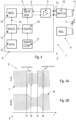
- FIG. 4 shows a transmitter 1 to transmit an amplitude modulated data signal 2 in an RF-Field 3 over the air to a receiver 4 of an RFID communication system 5 according to a first embodiment of the invention .
- the transmitter 1 comprises a wave generator 6 to generate a carrier signal 7 with a particular frequency and waveform.
- the RFID communication system 5 complies to the NFC Standard ISO 18.092 which defines a resonance frequency of the carrier signal 7 of 13,56 MHz with the waveform of a sinus.
- the RFID communication system 5 furthermore complies to ISO/IEC 14.443 Type A and B or ISO15.693 or ECMA-340 13,56 MHz.
- the wave generator 6 is realized in an integrated circuit 8 of transmitter 1 and provides the amplitude modulated data signal 2 via an amplifier 9 at Tx-Pins Tx of the integrated circuit 8.
- a matching circuit 10 is connected to the Tx-Pins Tx and matches the impedances to an antenna 11.
- the matching circuit 10 and the antenna 11 are arranged to transmit the amplified amplitude modulated data signal 2 in resonance to the close-by receiver 4 that could be realized as passive or active tag or any other active device like e.g. a mobile phone.
- a data stage 12 of the integrated circuit 8 stores digital data to be transmitted to the receiver 4.
- a modified Miller encoding has to be processed to encode the data signal of the digital data in an encoder stage 13, which provides an encoded data signal 14 to a modulation stage 15.
- the modulation stage 15 is built to steer the amplitude of the carrier signal 7 generated by the wave generator 6 to achieve a 10% Amplitude Shift Keying ASK modulation of the encoded data signal 14 to provide the amplitude modulated data signal 2 at the Tx-Pins Tx of the integrated circuit 8.
- a 50% or 100% ASK modulation or any other modulation or any other coding known to the man skilled in the art could be used.
- the transmitter 1 furthermore comprises a shape stage 16 connected to the wave generator 6 to select the waveform of the carrier signal 7 depending directly or indirectly on the data signal.
- the waveform is selected indirectly from the data signal as the encoded data signal is used.
- the shape stage 16 is connected to the encoder stage 13 and receives the encoded data signal 14 at the same time when it is provided to the modulation stage 15.
- the shape stage 16 therefor has the information when a rising or falling edge of the amplitude modulated data signal 2 shall occur.
- Figure 5A shows the amplitude modulated data signal 2 at Tx-Pins Tx that at a time instance t1 comprises a falling edge.
- Figure 5B shows the RF-Field generated by antenna 11 which RF-Field at time instance t2 would comprise an undershoot, if a transmitter know in the state of the art would be used as shown in figure 2B .
- the shape stage 16 is built to select another waveform in a second time frame after time instance t1 and shortly before the time instance t2 to provide more energy to the RF-Field 3.
- Such other waveforms to be selected by the shape stage 16 are stored in shape configuration stage 17, which stores waveforms with higher and lower energy content than the sinus waveform.
- a square waveform comprises more energy in the signal than the sinus waveform and the shape stage 16 selects a square waveform to replace one single sinus wave of the carrier signal 7 by one single square wave to avoid the undershoot in the envelope 18 of the amplitude modulated data signal 3 as shown in figure 5B .
- Figure 5A furthermore shows that the amplitude modulated data signal 2 at Tx-Pins Tx at time instance t3 comprises a rising edge.
- Figure 5B shows that the RF-Field at time instance t4 comprises as little overshoot that would be much higher, if a transmitter know in the state of the art would have been used, as shown in figure 2B .
- shape stage 16 is built to select another waveform in a first time frame after time instance t3 and shortly before the time instance t4 to provide less energy to the RF-Field 3.
- Such other waveforms to be selected by the shape stage 16 with less energy could be a sawtooth waveform or a triangular waveform to name just two possible waveforms, which waveforms are stored as configuration data in shape configuration stage 17.
- a sawtooth waveform with less energy in the signal than the sinus waveform is selected by shape stage 16, which replaces one single sinus wave of the carrier signal 7 by one single sawtooth wave to reduce the overshoot in the envelope 18 of the amplitude modulated data signal 3 as shown in figure 5B . If two sinus waves would have been replaced by two sawtooth waves the little overshoot shown in figure 5B could be avoided completely.
- Such a wave generator 6 that is able to generate a sinus waveform wave by wave is known from EP 3 182 585 B1 of the same applicant.
- This prior art document discloses a digital power amplifier which generates a sinus wave by small increments of M digital wave-forming bits which add up increments of output current to generate a sinus wave.
- all kind of other waveforms may be generated as well and a man skilled in the art will understand how to add up increments of M digital wave-forming bits to generate a triangular waveform instead of a sinus waveform. The same is true for other waveforms like the sawtooth waveform or even a rectangular waveform.
- the invention therefor is furthermore characterized in the inventive use of a digital power amplifier known from prior art mentioned above.
- the inventive use of the digital power amplifier is realized by the M digital wave-forming bits for different waveforms with higher or lower energy content in the signal wave stored in the shape configuration stage 17, which selected M digital wave-forming bits are used to steer the wave generator 6 by shape stage 16.
- the shape configuration stage 17 stores these M digital wave-forming bits for different waveforms in relation or combined with particular waveforms of the data signal or encoded data signal.
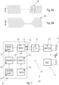
- Figure 6A shows a 100% amplitude modulated data signal on Tx-Pins Tx of the transmitter 1 shown in figure 4 with two triangular waves 19 inserted to avoid the overshoot in the envelope 20 of the RF-Field as shown in figure 6B .
- the waveform has been changed from the sinus to the triangular, to reduce the energy in the carrier signal, but in addition the amplitude of the triangular waves have been reduced compared to the amplitude of the sinus waves what in addition helps to reduce the overshoot in the envelope 20 of the RF-Field.
- the amplitude of the sinus waves may be increased in addition the change to a waveform with more energy content to avoid the undershoot.
- Figure 7 shows a transmitter 21 to transmit an amplitude modulated data signal 2 in an RF-Field 3 over the air to a receiver 4 of an RFID communication system 22 according to a second embodiment of the invention.
- the difference between transmitter 1 of the first embodiment and the transmitter 21 of the second embodiment is, that the wave generator 6 provides a carrier signal 7 with always the same amplitude and the amplitude modulation of this carrier signal 7 with the encoded data signal 14 is processed in modulation stage 15.
- amplifier 9 is not part of the integrated circuit 8, but realized as external amplifier 9 connected to Tx-Pins Tx.
- the data signal is not encoded and therefore directly used to modulate the carrier signal.
- the shape stage therefore selects the waveform of the carrier signal depending directly on the data signal.
- the wave generator could generate a sawtooth or triangular wave for the carrier signal used in general.
- the shape stage could in a second time frame use a sinus waveform with a higher energy content to avoid the undershoot in the envelope of the RF-Field.
- the wave generator could generate a square wave for the carrier signal used in general and a sinus waveform or sawtooth or triangular waveform with a lower energy content to avoid the overshoot in the envelope of the RF-Field.
- a man skilled in the art is able to provide all kind different selections of waveforms depending on what kind of waveform is used as general waveform for the carrier signal.
- a higher energy content of the carrier signal may be selected for one or several waves at the occurrence of a rising edge in the data signal or encoded data signal to reduce the time duration of the rising edge in the envelope of the RF-Field. This may cause an overshoot, what for some embodiments is not relevant, but the reduced time duration of the rising edge helps to e.g. increase the bit rate or ease the bit detection at the receiver.
- a lower energy content of the carrier signal may be selected for one or several waves at the occurrence of a falling edge in the data signal or encoded data signal to reduce the time duration of the falling edge in the envelope of the RF-Field. This may cause an undershoot, what for some embodiments is not relevant, but the reduced time duration of the falling edge helps to e.g. increase the bit rate or ease the bit detection at the receiver.
Landscapes
- Engineering & Computer Science (AREA)
- Computer Networks & Wireless Communication (AREA)
- Signal Processing (AREA)
- Digital Transmission Methods That Use Modulated Carrier Waves (AREA)
- Near-Field Transmission Systems (AREA)
- Power Engineering (AREA)
Claims (17)
- Émetteur (1 ; 21) pour transmettre un signal de données modulé en amplitude (2) dans un champ RF (3) par voie aérienne vers un récepteur (4) d'un système de communication RFID (5 ; 22), lequel émetteur (1 ; 21) comprend :un générateur d'ondes (6) pour générer un signal de porteuse (7) avec une fréquence et une forme d'onde particulières ;un étage de modulation (15) connectée au générateur d'ondes (6) pour orienter l'amplitude du signal de porteuse (7) par rapport à un signal de données à transmettre ;une antenne (11) connectée au générateur d'ondes (6) vi un amplificateur (9) et un circuit d'adaptation (10) pour transmettre le signal de données modulé en amplitude (2) dans le champ RF (3) par voie aérienne,caractérisé en ce que l'émetteur (1 ; 21) comprend en outre :un étage de forme (16) connecté au générateur d'ondes (6) pour choisir la forme d'onde du signal de porteuse (7) en fonction directement ou indirectement du signal de données,lequel étage de forme (16) est construit pour choisir dans une première trame temporelle (t3 -> t4) après le front montant du signal de données ou du signal de données codé (14) pendant le front montant de l'enveloppe (18 ; 20) du champ RF (3) une forme d'onde du signal de porteuse (7) avec la même fréquence, mais avec une teneur en énergie inférieure par rapport à l'extérieur de cette première trame temporelle (t3 > t4),lequel étage de forme (16) est construit pour choisir une forme d'onde triangulaire ou en dents de scie du signal de porteuse (7) dans la première trame temporelle (t3 > t4) et une forme d'onde sinusoïdale à l'extérieur de la première trame temporelle (t3 > t4).
- Émetteur (1 ; 21) selon la revendication 1, dans lequel l'émetteur (1 ; 21) comprend en outre un étage de codage (13) pour coder le signal de données afin de fournir un signal de données codé (14) à l'étage de modulation (15) afin de moduler le signal de porteuse (7) et pour fournir le signal de données codé (14) à l'étage de forme (16) afin de former la forme d'onde du signal de porteuse (7) dans une trame temporelle avant et/ou après le front montant et/ou le front descendant du signal de données codé (14).
- Émetteur (1 ; 21) selon la revendication 1 ou 2, dans lequel un étage de configuration de forme (17) stocke des données de configuration avec différentes formes d'onde du signal de porteuse (7) pour des formes d'onde particulières du signal de données et/ou du signal de données codé (14).
- Émetteur (1 ; 21) selon l'une quelconque des revendications 1 à 3, lequel étage de forme (16) étant construit pour choisir, dans une seconde trame temporelle (0 > t2) après le front descendant du signal de données ou du signal de données codé (14) pendant le front descendant de l'enveloppe (18) du champ RF (3), une forme d'onde du signal de porteuse (7) avec la même fréquence, mais avec une teneur en énergie plus élevée qu'à l'extérieur de cette seconde trame temporelle (t1 > t2).
- Émetteur (1 ; 21) selon la revendication 4, lequel étage de forme (16) étant construit pour choisir une forme d'onde carrée du signal de porteuse (7) à l'intérieur de la seconde trame temporelle (t1 > t2) et une forme d'onde sinusoïdale à l'extérieur de la seconde trame temporelle (t1 > t2).
- Émetteur (1 ; 21) selon l'une quelconque des revendications 1 à 5, dans lequel le générateur d'ondes (6) est construit pour générer un signal de porteuse (7) avec la fréquence NFC de 13,56 MHz.
- Émetteur (1 ; 21) selon les revendications 1 à 6, lequel étage de modulation (15) ou générateur d'ondes (6) réduisant en outre l'amplitude du signal de données ou du signal de données codé (14) dans des premières trames temporelles (t3 -> t4) pour éviter une suroscillation dans des premières trames temporelles (t3 -> t4), et augmentant en outre l'amplitude du signal de données ou du signal de données codé (14) dans des secondes trames temporelles (t1 -> t2) pour éviter une sous-oscillation dans des secondes trames temporelles (t1 - > t2).
- Émetteur (1 ; 21) pour transmettre un signal de données modulé en amplitude (2) dans un champ RF (3) par voie aérienne vers un récepteur (4) d'un système de communication RFID (5 ; 22), lequel émetteur (1 ; 21) comprend :un générateur d'ondes (6) pour générer un signal de porteuse (7) avec une fréquence et une forme d'onde particulières ;un étage de modulation (15) connectée au générateur d'ondes (6) pour moduler le signal de porteuse (7) par rapport à un signal de données à transmettre ;une antenne (11) connectée à l'étape de modulation (15) par l'intermédiaire d'un amplificateur (9) et d'un circuit d'adaptation (10) pour transmettre le signal de données modulé en amplitude (2) dans le champ RF (3) par voie aérienne,caractérisé en ce que l'émetteur (1 ; 21) comprend en outre :un étage de forme (16) connecté au générateur d'ondes (6) pour choisir la forme d'onde du signal de porteuse (7) en fonction directement ou indirectement du signal de données,lequel étage de forme (16) est construit pour choisir dans une première trame temporelle (t3 -> t4) après le front montant du signal de données ou du signal de données codé (14) pendant le front montant de l'enveloppe (18 ; 20) du champ RF (3) une forme d'onde du signal de porteuse (7) avec la même fréquence, mais avec une teneur en énergie inférieure par rapport à l'extérieur de cette première trame temporelle (t3 > t4),lequel étage de forme (16) est construit pour choisir une forme d'onde triangulaire ou en dents de scie du signal de porteuse (7) dans la première trame temporelle (t3 > t4) et une forme d'onde sinusoïdale à l'extérieur de la première trame temporelle (t3 > t4).
- Émetteur (1 ; 21) selon la revendication 8, dans lequel l'émetteur (1 ; 21) comprend en outre un étage de codage (13) pour coder le signal de données afin de fournir un signal de données codé (14) à l'étage de modulation (15) afin de moduler le signal de porteuse (7) et pour fournir le signal de données codé (14) à l'étage de forme (16) afin de former la forme d'onde du signal de porteuse (7) dans une trame temporelle avant et/ou après le front montant et/ou le front descendant du signal de données codé (14).
- Émetteur (1 ; 21) selon la revendication 8 ou 9, dans lequel un étage de configuration de forme (17) stocke des données de configuration avec différentes formes d'onde du signal de porteuse (7) pour des formes d'onde particulières du signal de données et/ou du signal de données codé (14).
- Émetteur (1 ; 21) selon l'une quelconque des revendications 8 à 10, lequel étage de forme (16) étant construit pour choisir, dans une seconde trame temporelle (t1 > t2) après le front descendant du signal de données ou du signal de données codé (14) pendant le front descendant de l'enveloppe (18) du champ RF (3), une forme d'onde du signal de porteuse (7) avec la même fréquence, mais avec une teneur en énergie plus élevée qu'à l'extérieur de cette seconde trame temporelle (t1 > t2).
- Émetteur (1 ; 21) selon la revendication 11, lequel étage de forme (16) étant construit pour choisir une forme d'onde carrée du signal de porteuse (7) à l'intérieur de la seconde trame temporelle (t1 > t2) et une forme d'onde sinusoïdale à l'extérieur de la seconde trame temporelle (t1 > t2).
- Émetteur (1 ; 21) selon l'une quelconque des revendications 8 à 12, dans lequel le générateur d'ondes (6) est construit pour générer un signal de porteuse (7) avec la fréquence NFC de 13,56 MHz.
- Émetteur (1 ; 21) selon les revendications 8 à 13, lequel étage de modulation (15) ou générateur d'ondes (6) réduisant en outre l'amplitude du signal de données ou du signal de données codé (14) dans des premières trames temporelles (t3 -> t4) pour éviter une suroscillation dans des premières trames temporelles (t3 -> t4), et augmentant en outre l'amplitude du signal de données ou du signal de données codé (14) dans des secondes trames temporelles (t1 -> t2) pour éviter une sous-oscillation dans des secondes trames temporelles (t1 - > t2).
- Procédé pour utiliser un émetteur (1 ; 21) selon l'une quelconque des revendications 1 à 7 ou l'une quelconque des revendications 8 à 14 afin de transmettre un signal de données modulé en amplitude (2) dans un champ RF (3) par voie aérienne vers un récepteur (4) d'un système de communication RFID (5 ; 22), lequel procédé comprend les étapes suivantes consistant à :traiter une modulation d'amplitude d'un signal de porteuse (7) avec une fréquence et une forme d'onde particulières avec un signal de données ou un signal de données codé (14) à transmettre ;choisir une forme d'onde différente avec un contenu d'énergie supérieur ou inférieur du signal de porteuse (7) pour une ou plusieurs ondes en fonction de l'apparition d'un front montant ou d'un front descendant dans le signal de données ou le signal de données codé (14).
- Procédé selon la revendication 15, dans lequel une teneur en énergie inférieure du signal de porteuse (7) pour une ou plusieurs ondes lors de l'apparition d'un front montant dans le signal de données ou le signal de données codé (14) est choisie pour réduire ou éviter une suroscillation dans l'enveloppe (18 ; 20) du champ RF (3), ou dans lequel une teneur en énergie supérieure du signal de porteuse (7) pour une ou plusieurs ondes lors de l'apparition d'un front descendant dans le signal de données ou le signal de données codé (14) est choisie pour réduire ou éviter une sous-oscillation dans l'enveloppe (18 ; 20) du champ RF (3).
- Procédé selon la revendication 15, dans lequel une teneur en énergie plus élevée du signal de porteuse (7) pour une ou plusieurs ondes lors de l'apparition d'un front montant dans le signal de données ou le signal de données codé (14) est choisie pour réduire la durée du front montant dans l'enveloppe (18 ; 20) du champ RF (3), ou dans lequel une teneur en énergie plus faible du signal de porteuse (7) pour une ou plusieurs ondes lors de l'apparition d'un front descendant dans le signal de données ou le signal de données codé (14) est choisie pour réduire la durée du front descendant dans l'enveloppe (18 ; 20) du champ RF (3).
Priority Applications (4)
| Application Number | Priority Date | Filing Date | Title |
|---|---|---|---|
| EP20213183.5A EP4012935B1 (fr) | 2020-12-10 | 2020-12-10 | Mise en forme d'ondes pour la prévention de la sous-oscillation et de la sur-oscillation |
| US17/502,881 US11909426B2 (en) | 2020-12-10 | 2021-10-15 | Wave-shaping for over- and undershoot prevention |
| JP2021198977A JP7751471B2 (ja) | 2020-12-10 | 2021-12-08 | オーバーシュートおよびアンダーシュート防止のための波形成形 |
| CN202111492140.1A CN114629508B (zh) | 2020-12-10 | 2021-12-08 | 用于防止过冲和下冲的波形整形 |
Applications Claiming Priority (1)
| Application Number | Priority Date | Filing Date | Title |
|---|---|---|---|
| EP20213183.5A EP4012935B1 (fr) | 2020-12-10 | 2020-12-10 | Mise en forme d'ondes pour la prévention de la sous-oscillation et de la sur-oscillation |
Publications (2)
| Publication Number | Publication Date |
|---|---|
| EP4012935A1 EP4012935A1 (fr) | 2022-06-15 |
| EP4012935B1 true EP4012935B1 (fr) | 2023-08-02 |
Family
ID=73793129
Family Applications (1)
| Application Number | Title | Priority Date | Filing Date |
|---|---|---|---|
| EP20213183.5A Active EP4012935B1 (fr) | 2020-12-10 | 2020-12-10 | Mise en forme d'ondes pour la prévention de la sous-oscillation et de la sur-oscillation |
Country Status (4)
| Country | Link |
|---|---|
| US (1) | US11909426B2 (fr) |
| EP (1) | EP4012935B1 (fr) |
| JP (1) | JP7751471B2 (fr) |
| CN (1) | CN114629508B (fr) |
Family Cites Families (11)
| Publication number | Priority date | Publication date | Assignee | Title |
|---|---|---|---|---|
| JP3891421B2 (ja) * | 2002-10-16 | 2007-03-14 | ソニー株式会社 | 電子回路、変調方法、並びに、情報処理装置および方法 |
| GB0413563D0 (en) * | 2004-06-17 | 2004-07-21 | Roke Manor Research | Shaped pulse |
| US7773028B2 (en) * | 2006-12-06 | 2010-08-10 | Raytheon Company | Method and system for concatenation of radar pulses |
| EP2608401B1 (fr) * | 2011-12-21 | 2019-03-27 | EM Microelectronic-Marin SA | Circuit de transmission de signaux RF ASK avec adaptation des flancs des signaux de données |
| US9450649B2 (en) * | 2012-07-02 | 2016-09-20 | Marvell World Trade Ltd. | Shaping near-field transmission signals |
| US8902965B2 (en) * | 2012-09-27 | 2014-12-02 | Qualcomm Incorporated | Pulse shaping for generating NFC initiator transmit waveform |
| EP3080916B1 (fr) * | 2013-12-13 | 2018-08-29 | Clairvoyant Technology LLC | Synthèse de forme d'onde pour émetteurs rfid |
| EP3182585B1 (fr) | 2015-12-14 | 2020-07-22 | Panthronics AG | Amplificateur de puissance numérique haute tension avec sortie sinusoïdale pour rfid |
| US9654181B1 (en) | 2015-12-14 | 2017-05-16 | Nxp B.V. | Dynamic transmitter signal envelope shaping control for NFC or RFID devices |
| JP2017191592A (ja) * | 2016-04-06 | 2017-10-19 | 東芝テック株式会社 | 無線タグ装置、無線タグ通信装置、無線タグ通信システム |
| US10170287B1 (en) * | 2017-10-16 | 2019-01-01 | Taiwan Semiconductor Manufacturing Co., Ltd. | Techniques for detecting micro-arcing occurring inside a semiconductor processing chamber |
-
2020
- 2020-12-10 EP EP20213183.5A patent/EP4012935B1/fr active Active
-
2021
- 2021-10-15 US US17/502,881 patent/US11909426B2/en active Active
- 2021-12-08 CN CN202111492140.1A patent/CN114629508B/zh active Active
- 2021-12-08 JP JP2021198977A patent/JP7751471B2/ja active Active
Also Published As
| Publication number | Publication date |
|---|---|
| CN114629508B (zh) | 2025-02-11 |
| JP2022092601A (ja) | 2022-06-22 |
| JP7751471B2 (ja) | 2025-10-08 |
| EP4012935A1 (fr) | 2022-06-15 |
| US11909426B2 (en) | 2024-02-20 |
| CN114629508A (zh) | 2022-06-14 |
| US20220190792A1 (en) | 2022-06-16 |
Similar Documents
| Publication | Publication Date | Title |
|---|---|---|
| US11017187B1 (en) | Fast frequency switching for RFID applications | |
| EP3182585B1 (fr) | Amplificateur de puissance numérique haute tension avec sortie sinusoïdale pour rfid | |
| EP3145092B1 (fr) | Procédé et circuit de transmission de communication par modulation de charge active dans des systèmes d'identification par radiofréquence | |
| US7994659B2 (en) | Method for supplying electrical energy from a first electronic circuit to a second electronic circuit via at least one wire line | |
| US9178731B2 (en) | Transmission apparatus for a wireless device using delta-sigma modulation | |
| US10419254B2 (en) | Transmission apparatus for a wireless device using delta-sigma modulation | |
| US9654186B2 (en) | Portable terminal | |
| US8552841B2 (en) | Communication method having selectable response signal strength levels | |
| EP4012935B1 (fr) | Mise en forme d'ondes pour la prévention de la sous-oscillation et de la sur-oscillation | |
| EP3142311B1 (fr) | Conformation d'impulsions pour émetteurs à fréquence radioélectrique | |
| EP3605854B1 (fr) | Étalonnage d'émetteur pour un dispositif de communication en champ proche (nfc) | |
| US11444591B2 (en) | Device and method for a wireless transmitter | |
| JP4384654B2 (ja) | 無線識別タグの単側波帯域応答方法 | |
| EP3751462B1 (fr) | Transpondeur et procédé de fonctionnement correspondant | |
| EP1388932B1 (fr) | Modulateur commutaté | |
| US20260045925A1 (en) | Device and method for receiving 1-bit amplitude-modulated signals | |
| KR100961672B1 (ko) | 비접촉 송/수신 시스템에 의해 전송되는 전자기 신호를 위한 모듈레이터 장치 |
Legal Events
| Date | Code | Title | Description |
|---|---|---|---|
| PUAI | Public reference made under article 153(3) epc to a published international application that has entered the european phase |
Free format text: ORIGINAL CODE: 0009012 |
|
| STAA | Information on the status of an ep patent application or granted ep patent |
Free format text: STATUS: REQUEST FOR EXAMINATION WAS MADE |
|
| 17P | Request for examination filed |
Effective date: 20220127 |
|
| AK | Designated contracting states |
Kind code of ref document: A1 Designated state(s): AL AT BE BG CH CY CZ DE DK EE ES FI FR GB GR HR HU IE IS IT LI LT LU LV MC MK MT NL NO PL PT RO RS SE SI SK SM TR |
|
| GRAP | Despatch of communication of intention to grant a patent |
Free format text: ORIGINAL CODE: EPIDOSNIGR1 |
|
| STAA | Information on the status of an ep patent application or granted ep patent |
Free format text: STATUS: GRANT OF PATENT IS INTENDED |
|
| INTG | Intention to grant announced |
Effective date: 20230329 |
|
| GRAS | Grant fee paid |
Free format text: ORIGINAL CODE: EPIDOSNIGR3 |
|
| GRAA | (expected) grant |
Free format text: ORIGINAL CODE: 0009210 |
|
| STAA | Information on the status of an ep patent application or granted ep patent |
Free format text: STATUS: THE PATENT HAS BEEN GRANTED |
|
| AK | Designated contracting states |
Kind code of ref document: B1 Designated state(s): AL AT BE BG CH CY CZ DE DK EE ES FI FR GB GR HR HU IE IS IT LI LT LU LV MC MK MT NL NO PL PT RO RS SE SI SK SM TR |
|
| REG | Reference to a national code |
Ref country code: GB Ref legal event code: FG4D |
|
| REG | Reference to a national code |
Ref country code: CH Ref legal event code: EP |
|
| REG | Reference to a national code |
Ref country code: DE Ref legal event code: R096 Ref document number: 602020014876 Country of ref document: DE |
|
| REG | Reference to a national code |
Ref country code: IE Ref legal event code: FG4D |
|
| REG | Reference to a national code |
Ref country code: DE Ref legal event code: R081 Ref document number: 602020014876 Country of ref document: DE Owner name: RENESAS DESIGN AUSTRIA GMBH, AT Free format text: FORMER OWNER: PANTHRONICS AG, GRAZ, AT Ref country code: LT Ref legal event code: MG9D |
|
| REG | Reference to a national code |
Ref country code: NL Ref legal event code: MP Effective date: 20230802 |
|
| RAP4 | Party data changed (patent owner data changed or rights of a patent transferred) |
Owner name: RENESAS DESIGN AUSTRIA GMBH |
|
| REG | Reference to a national code |
Ref country code: AT Ref legal event code: MK05 Ref document number: 1595982 Country of ref document: AT Kind code of ref document: T Effective date: 20230802 |
|
| PG25 | Lapsed in a contracting state [announced via postgrant information from national office to epo] |
Ref country code: GR Free format text: LAPSE BECAUSE OF FAILURE TO SUBMIT A TRANSLATION OF THE DESCRIPTION OR TO PAY THE FEE WITHIN THE PRESCRIBED TIME-LIMIT Effective date: 20231103 |
|
| PG25 | Lapsed in a contracting state [announced via postgrant information from national office to epo] |
Ref country code: IS Free format text: LAPSE BECAUSE OF FAILURE TO SUBMIT A TRANSLATION OF THE DESCRIPTION OR TO PAY THE FEE WITHIN THE PRESCRIBED TIME-LIMIT Effective date: 20231202 |
|
| PG25 | Lapsed in a contracting state [announced via postgrant information from national office to epo] |
Ref country code: SE Free format text: LAPSE BECAUSE OF FAILURE TO SUBMIT A TRANSLATION OF THE DESCRIPTION OR TO PAY THE FEE WITHIN THE PRESCRIBED TIME-LIMIT Effective date: 20230802 Ref country code: RS Free format text: LAPSE BECAUSE OF FAILURE TO SUBMIT A TRANSLATION OF THE DESCRIPTION OR TO PAY THE FEE WITHIN THE PRESCRIBED TIME-LIMIT Effective date: 20230802 Ref country code: PT Free format text: LAPSE BECAUSE OF FAILURE TO SUBMIT A TRANSLATION OF THE DESCRIPTION OR TO PAY THE FEE WITHIN THE PRESCRIBED TIME-LIMIT Effective date: 20231204 Ref country code: NO Free format text: LAPSE BECAUSE OF FAILURE TO SUBMIT A TRANSLATION OF THE DESCRIPTION OR TO PAY THE FEE WITHIN THE PRESCRIBED TIME-LIMIT Effective date: 20231102 Ref country code: NL Free format text: LAPSE BECAUSE OF FAILURE TO SUBMIT A TRANSLATION OF THE DESCRIPTION OR TO PAY THE FEE WITHIN THE PRESCRIBED TIME-LIMIT Effective date: 20230802 Ref country code: LV Free format text: LAPSE BECAUSE OF FAILURE TO SUBMIT A TRANSLATION OF THE DESCRIPTION OR TO PAY THE FEE WITHIN THE PRESCRIBED TIME-LIMIT Effective date: 20230802 Ref country code: LT Free format text: LAPSE BECAUSE OF FAILURE TO SUBMIT A TRANSLATION OF THE DESCRIPTION OR TO PAY THE FEE WITHIN THE PRESCRIBED TIME-LIMIT Effective date: 20230802 Ref country code: IS Free format text: LAPSE BECAUSE OF FAILURE TO SUBMIT A TRANSLATION OF THE DESCRIPTION OR TO PAY THE FEE WITHIN THE PRESCRIBED TIME-LIMIT Effective date: 20231202 Ref country code: HR Free format text: LAPSE BECAUSE OF FAILURE TO SUBMIT A TRANSLATION OF THE DESCRIPTION OR TO PAY THE FEE WITHIN THE PRESCRIBED TIME-LIMIT Effective date: 20230802 Ref country code: GR Free format text: LAPSE BECAUSE OF FAILURE TO SUBMIT A TRANSLATION OF THE DESCRIPTION OR TO PAY THE FEE WITHIN THE PRESCRIBED TIME-LIMIT Effective date: 20231103 Ref country code: FI Free format text: LAPSE BECAUSE OF FAILURE TO SUBMIT A TRANSLATION OF THE DESCRIPTION OR TO PAY THE FEE WITHIN THE PRESCRIBED TIME-LIMIT Effective date: 20230802 Ref country code: AT Free format text: LAPSE BECAUSE OF FAILURE TO SUBMIT A TRANSLATION OF THE DESCRIPTION OR TO PAY THE FEE WITHIN THE PRESCRIBED TIME-LIMIT Effective date: 20230802 |
|
| PG25 | Lapsed in a contracting state [announced via postgrant information from national office to epo] |
Ref country code: PL Free format text: LAPSE BECAUSE OF FAILURE TO SUBMIT A TRANSLATION OF THE DESCRIPTION OR TO PAY THE FEE WITHIN THE PRESCRIBED TIME-LIMIT Effective date: 20230802 |
|
| PG25 | Lapsed in a contracting state [announced via postgrant information from national office to epo] |
Ref country code: ES Free format text: LAPSE BECAUSE OF FAILURE TO SUBMIT A TRANSLATION OF THE DESCRIPTION OR TO PAY THE FEE WITHIN THE PRESCRIBED TIME-LIMIT Effective date: 20230802 |
|
| PG25 | Lapsed in a contracting state [announced via postgrant information from national office to epo] |
Ref country code: SM Free format text: LAPSE BECAUSE OF FAILURE TO SUBMIT A TRANSLATION OF THE DESCRIPTION OR TO PAY THE FEE WITHIN THE PRESCRIBED TIME-LIMIT Effective date: 20230802 Ref country code: RO Free format text: LAPSE BECAUSE OF FAILURE TO SUBMIT A TRANSLATION OF THE DESCRIPTION OR TO PAY THE FEE WITHIN THE PRESCRIBED TIME-LIMIT Effective date: 20230802 Ref country code: ES Free format text: LAPSE BECAUSE OF FAILURE TO SUBMIT A TRANSLATION OF THE DESCRIPTION OR TO PAY THE FEE WITHIN THE PRESCRIBED TIME-LIMIT Effective date: 20230802 Ref country code: EE Free format text: LAPSE BECAUSE OF FAILURE TO SUBMIT A TRANSLATION OF THE DESCRIPTION OR TO PAY THE FEE WITHIN THE PRESCRIBED TIME-LIMIT Effective date: 20230802 Ref country code: DK Free format text: LAPSE BECAUSE OF FAILURE TO SUBMIT A TRANSLATION OF THE DESCRIPTION OR TO PAY THE FEE WITHIN THE PRESCRIBED TIME-LIMIT Effective date: 20230802 Ref country code: CZ Free format text: LAPSE BECAUSE OF FAILURE TO SUBMIT A TRANSLATION OF THE DESCRIPTION OR TO PAY THE FEE WITHIN THE PRESCRIBED TIME-LIMIT Effective date: 20230802 Ref country code: SK Free format text: LAPSE BECAUSE OF FAILURE TO SUBMIT A TRANSLATION OF THE DESCRIPTION OR TO PAY THE FEE WITHIN THE PRESCRIBED TIME-LIMIT Effective date: 20230802 |
|
| REG | Reference to a national code |
Ref country code: DE Ref legal event code: R097 Ref document number: 602020014876 Country of ref document: DE |
|
| PG25 | Lapsed in a contracting state [announced via postgrant information from national office to epo] |
Ref country code: IT Free format text: LAPSE BECAUSE OF FAILURE TO SUBMIT A TRANSLATION OF THE DESCRIPTION OR TO PAY THE FEE WITHIN THE PRESCRIBED TIME-LIMIT Effective date: 20230802 |
|
| PLBE | No opposition filed within time limit |
Free format text: ORIGINAL CODE: 0009261 |
|
| STAA | Information on the status of an ep patent application or granted ep patent |
Free format text: STATUS: NO OPPOSITION FILED WITHIN TIME LIMIT |
|
| 26N | No opposition filed |
Effective date: 20240503 |
|
| PG25 | Lapsed in a contracting state [announced via postgrant information from national office to epo] |
Ref country code: SI Free format text: LAPSE BECAUSE OF FAILURE TO SUBMIT A TRANSLATION OF THE DESCRIPTION OR TO PAY THE FEE WITHIN THE PRESCRIBED TIME-LIMIT Effective date: 20230802 |
|
| REG | Reference to a national code |
Ref country code: CH Ref legal event code: PL |
|
| PG25 | Lapsed in a contracting state [announced via postgrant information from national office to epo] |
Ref country code: LU Free format text: LAPSE BECAUSE OF NON-PAYMENT OF DUE FEES Effective date: 20231210 |
|
| PG25 | Lapsed in a contracting state [announced via postgrant information from national office to epo] |
Ref country code: MC Free format text: LAPSE BECAUSE OF FAILURE TO SUBMIT A TRANSLATION OF THE DESCRIPTION OR TO PAY THE FEE WITHIN THE PRESCRIBED TIME-LIMIT Effective date: 20230802 |
|
| REG | Reference to a national code |
Ref country code: BE Ref legal event code: MM Effective date: 20231231 |
|
| PG25 | Lapsed in a contracting state [announced via postgrant information from national office to epo] |
Ref country code: MC Free format text: LAPSE BECAUSE OF FAILURE TO SUBMIT A TRANSLATION OF THE DESCRIPTION OR TO PAY THE FEE WITHIN THE PRESCRIBED TIME-LIMIT Effective date: 20230802 Ref country code: LU Free format text: LAPSE BECAUSE OF NON-PAYMENT OF DUE FEES Effective date: 20231210 |
|
| REG | Reference to a national code |
Ref country code: IE Ref legal event code: MM4A |
|
| PG25 | Lapsed in a contracting state [announced via postgrant information from national office to epo] |
Ref country code: IE Free format text: LAPSE BECAUSE OF NON-PAYMENT OF DUE FEES Effective date: 20231210 |
|
| PG25 | Lapsed in a contracting state [announced via postgrant information from national office to epo] |
Ref country code: BE Free format text: LAPSE BECAUSE OF NON-PAYMENT OF DUE FEES Effective date: 20231231 |
|
| PG25 | Lapsed in a contracting state [announced via postgrant information from national office to epo] |
Ref country code: FR Free format text: LAPSE BECAUSE OF NON-PAYMENT OF DUE FEES Effective date: 20231231 |
|
| PG25 | Lapsed in a contracting state [announced via postgrant information from national office to epo] |
Ref country code: CH Free format text: LAPSE BECAUSE OF NON-PAYMENT OF DUE FEES Effective date: 20231231 |
|
| PG25 | Lapsed in a contracting state [announced via postgrant information from national office to epo] |
Ref country code: IE Free format text: LAPSE BECAUSE OF NON-PAYMENT OF DUE FEES Effective date: 20231210 Ref country code: FR Free format text: LAPSE BECAUSE OF NON-PAYMENT OF DUE FEES Effective date: 20231231 Ref country code: CH Free format text: LAPSE BECAUSE OF NON-PAYMENT OF DUE FEES Effective date: 20231231 Ref country code: BE Free format text: LAPSE BECAUSE OF NON-PAYMENT OF DUE FEES Effective date: 20231231 |
|
| PG25 | Lapsed in a contracting state [announced via postgrant information from national office to epo] |
Ref country code: BG Free format text: LAPSE BECAUSE OF FAILURE TO SUBMIT A TRANSLATION OF THE DESCRIPTION OR TO PAY THE FEE WITHIN THE PRESCRIBED TIME-LIMIT Effective date: 20230802 |
|
| PG25 | Lapsed in a contracting state [announced via postgrant information from national office to epo] |
Ref country code: BG Free format text: LAPSE BECAUSE OF FAILURE TO SUBMIT A TRANSLATION OF THE DESCRIPTION OR TO PAY THE FEE WITHIN THE PRESCRIBED TIME-LIMIT Effective date: 20230802 |
|
| PG25 | Lapsed in a contracting state [announced via postgrant information from national office to epo] |
Ref country code: CY Free format text: LAPSE BECAUSE OF FAILURE TO SUBMIT A TRANSLATION OF THE DESCRIPTION OR TO PAY THE FEE WITHIN THE PRESCRIBED TIME-LIMIT; INVALID AB INITIO Effective date: 20201210 |
|
| PG25 | Lapsed in a contracting state [announced via postgrant information from national office to epo] |
Ref country code: HU Free format text: LAPSE BECAUSE OF FAILURE TO SUBMIT A TRANSLATION OF THE DESCRIPTION OR TO PAY THE FEE WITHIN THE PRESCRIBED TIME-LIMIT; INVALID AB INITIO Effective date: 20201210 |
|
| GBPC | Gb: european patent ceased through non-payment of renewal fee |
Effective date: 20241210 |
|
| PG25 | Lapsed in a contracting state [announced via postgrant information from national office to epo] |
Ref country code: GB Free format text: LAPSE BECAUSE OF NON-PAYMENT OF DUE FEES Effective date: 20241210 |
|
| PG25 | Lapsed in a contracting state [announced via postgrant information from national office to epo] |
Ref country code: TR Free format text: LAPSE BECAUSE OF FAILURE TO SUBMIT A TRANSLATION OF THE DESCRIPTION OR TO PAY THE FEE WITHIN THE PRESCRIBED TIME-LIMIT Effective date: 20230802 |
|
| PGFP | Annual fee paid to national office [announced via postgrant information from national office to epo] |
Ref country code: DE Payment date: 20251222 Year of fee payment: 6 |