EP4014323B1 - Émetteur à modulation polaire avec commande de mode de produit à large bande - Google Patents
Émetteur à modulation polaire avec commande de mode de produit à large bande Download PDFInfo
- Publication number
- EP4014323B1 EP4014323B1 EP20853444.6A EP20853444A EP4014323B1 EP 4014323 B1 EP4014323 B1 EP 4014323B1 EP 20853444 A EP20853444 A EP 20853444A EP 4014323 B1 EP4014323 B1 EP 4014323B1
- Authority
- EP
- European Patent Office
- Prior art keywords
- mode
- magnitude
- driver
- voltage
- drv
- Prior art date
- Legal status (The legal status is an assumption and is not a legal conclusion. Google has not performed a legal analysis and makes no representation as to the accuracy of the status listed.)
- Active
Links
Images




Classifications
-
- H—ELECTRICITY
- H04—ELECTRIC COMMUNICATION TECHNIQUE
- H04B—TRANSMISSION
- H04B1/00—Details of transmission systems, not covered by a single one of groups H04B3/00 - H04B13/00; Details of transmission systems not characterised by the medium used for transmission
- H04B1/02—Transmitters
- H04B1/04—Circuits
-
- H—ELECTRICITY
- H03—ELECTRONIC CIRCUITRY
- H03F—AMPLIFIERS
- H03F1/00—Details of amplifiers with only discharge tubes, only semiconductor devices or only unspecified devices as amplifying elements
- H03F1/02—Modifications of amplifiers to raise the efficiency, e.g. gliding Class A stages, use of an auxiliary oscillation
- H03F1/0205—Modifications of amplifiers to raise the efficiency, e.g. gliding Class A stages, use of an auxiliary oscillation in transistor amplifiers
- H03F1/0211—Modifications of amplifiers to raise the efficiency, e.g. gliding Class A stages, use of an auxiliary oscillation in transistor amplifiers with control of the supply voltage or current
- H03F1/0216—Continuous control
- H03F1/0222—Continuous control by using a signal derived from the input signal
- H03F1/0227—Continuous control by using a signal derived from the input signal using supply converters
-
- H—ELECTRICITY
- H03—ELECTRONIC CIRCUITRY
- H03F—AMPLIFIERS
- H03F1/00—Details of amplifiers with only discharge tubes, only semiconductor devices or only unspecified devices as amplifying elements
- H03F1/02—Modifications of amplifiers to raise the efficiency, e.g. gliding Class A stages, use of an auxiliary oscillation
- H03F1/0205—Modifications of amplifiers to raise the efficiency, e.g. gliding Class A stages, use of an auxiliary oscillation in transistor amplifiers
- H03F1/0211—Modifications of amplifiers to raise the efficiency, e.g. gliding Class A stages, use of an auxiliary oscillation in transistor amplifiers with control of the supply voltage or current
- H03F1/0244—Stepped control
- H03F1/025—Stepped control by using a signal derived from the input signal
-
- H—ELECTRICITY
- H03—ELECTRONIC CIRCUITRY
- H03F—AMPLIFIERS
- H03F1/00—Details of amplifiers with only discharge tubes, only semiconductor devices or only unspecified devices as amplifying elements
- H03F1/42—Modifications of amplifiers to extend the bandwidth
-
- H—ELECTRICITY
- H03—ELECTRONIC CIRCUITRY
- H03F—AMPLIFIERS
- H03F3/00—Amplifiers with only discharge tubes or only semiconductor devices as amplifying elements
- H03F3/189—High-frequency amplifiers, e.g. radio frequency amplifiers
- H03F3/19—High-frequency amplifiers, e.g. radio frequency amplifiers with semiconductor devices only
- H03F3/193—High-frequency amplifiers, e.g. radio frequency amplifiers with semiconductor devices only with field-effect devices
-
- H—ELECTRICITY
- H03—ELECTRONIC CIRCUITRY
- H03F—AMPLIFIERS
- H03F3/00—Amplifiers with only discharge tubes or only semiconductor devices as amplifying elements
- H03F3/20—Power amplifiers, e.g. Class B amplifiers, Class C amplifiers
- H03F3/21—Power amplifiers, e.g. Class B amplifiers, Class C amplifiers with semiconductor devices only
- H03F3/211—Power amplifiers, e.g. Class B amplifiers, Class C amplifiers with semiconductor devices only using a combination of several amplifiers
-
- H—ELECTRICITY
- H03—ELECTRONIC CIRCUITRY
- H03F—AMPLIFIERS
- H03F3/00—Amplifiers with only discharge tubes or only semiconductor devices as amplifying elements
- H03F3/20—Power amplifiers, e.g. Class B amplifiers, Class C amplifiers
- H03F3/21—Power amplifiers, e.g. Class B amplifiers, Class C amplifiers with semiconductor devices only
- H03F3/217—Class D power amplifiers; Switching amplifiers
- H03F3/2171—Class D power amplifiers; Switching amplifiers with field-effect devices
-
- H—ELECTRICITY
- H03—ELECTRONIC CIRCUITRY
- H03F—AMPLIFIERS
- H03F3/00—Amplifiers with only discharge tubes or only semiconductor devices as amplifying elements
- H03F3/20—Power amplifiers, e.g. Class B amplifiers, Class C amplifiers
- H03F3/21—Power amplifiers, e.g. Class B amplifiers, Class C amplifiers with semiconductor devices only
- H03F3/217—Class D power amplifiers; Switching amplifiers
- H03F3/2178—Class D power amplifiers; Switching amplifiers using more than one switch or switching amplifier in parallel or in series
-
- H—ELECTRICITY
- H03—ELECTRONIC CIRCUITRY
- H03F—AMPLIFIERS
- H03F3/00—Amplifiers with only discharge tubes or only semiconductor devices as amplifying elements
- H03F3/20—Power amplifiers, e.g. Class B amplifiers, Class C amplifiers
- H03F3/24—Power amplifiers, e.g. Class B amplifiers, Class C amplifiers of transmitter output stages
- H03F3/245—Power amplifiers, e.g. Class B amplifiers, Class C amplifiers of transmitter output stages with semiconductor devices only
-
- H—ELECTRICITY
- H04—ELECTRIC COMMUNICATION TECHNIQUE
- H04B—TRANSMISSION
- H04B1/00—Details of transmission systems, not covered by a single one of groups H04B3/00 - H04B13/00; Details of transmission systems not characterised by the medium used for transmission
- H04B1/02—Transmitters
- H04B1/04—Circuits
- H04B1/0475—Circuits with means for limiting noise, interference or distortion
-
- H—ELECTRICITY
- H04—ELECTRIC COMMUNICATION TECHNIQUE
- H04L—TRANSMISSION OF DIGITAL INFORMATION, e.g. TELEGRAPHIC COMMUNICATION
- H04L27/00—Modulated-carrier systems
- H04L27/10—Frequency-modulated carrier systems, i.e. using frequency-shift keying
- H04L27/12—Modulator circuits; Transmitter circuits
-
- H—ELECTRICITY
- H04—ELECTRIC COMMUNICATION TECHNIQUE
- H04L—TRANSMISSION OF DIGITAL INFORMATION, e.g. TELEGRAPHIC COMMUNICATION
- H04L27/00—Modulated-carrier systems
- H04L27/32—Carrier systems characterised by combinations of two or more of the types covered by groups H04L27/02, H04L27/10, H04L27/18 or H04L27/26
- H04L27/34—Amplitude- and phase-modulated carrier systems, e.g. quadrature-amplitude modulated carrier systems
- H04L27/36—Modulator circuits; Transmitter circuits
- H04L27/361—Modulation using a single or unspecified number of carriers, e.g. with separate stages of phase and amplitude modulation
-
- H—ELECTRICITY
- H03—ELECTRONIC CIRCUITRY
- H03F—AMPLIFIERS
- H03F2200/00—Indexing scheme relating to amplifiers
- H03F2200/324—An amplitude modulator or demodulator being used in the amplifier circuit
-
- H—ELECTRICITY
- H03—ELECTRONIC CIRCUITRY
- H03F—AMPLIFIERS
- H03F2200/00—Indexing scheme relating to amplifiers
- H03F2200/451—Indexing scheme relating to amplifiers the amplifier being a radio frequency amplifier
-
- H—ELECTRICITY
- H03—ELECTRONIC CIRCUITRY
- H03F—AMPLIFIERS
- H03F2200/00—Indexing scheme relating to amplifiers
- H03F2200/69—Indexing scheme relating to amplifiers the amplifier stage being a common drain coupled MOSFET, i.e. source follower
-
- H—ELECTRICITY
- H04—ELECTRIC COMMUNICATION TECHNIQUE
- H04B—TRANSMISSION
- H04B1/00—Details of transmission systems, not covered by a single one of groups H04B3/00 - H04B13/00; Details of transmission systems not characterised by the medium used for transmission
- H04B1/02—Transmitters
- H04B1/04—Circuits
- H04B2001/0408—Circuits with power amplifiers
-
- H—ELECTRICITY
- H04—ELECTRIC COMMUNICATION TECHNIQUE
- H04B—TRANSMISSION
- H04B1/00—Details of transmission systems, not covered by a single one of groups H04B3/00 - H04B13/00; Details of transmission systems not characterised by the medium used for transmission
- H04B1/02—Transmitters
- H04B1/04—Circuits
- H04B2001/0408—Circuits with power amplifiers
- H04B2001/045—Circuits with power amplifiers with means for improving efficiency
Definitions
- Modem radio frequency (RF) communications systems employ complex modulation schemes in which both the magnitude and the angle (phase or frequency) of an RF carrier are modulated to convey information. These complex modulation schemes are used since they increase spectral efficiency. However, they also make it difficult to design an RF transmitter that is energy efficient. Energy efficiency is particularly important in RF transmitters that are battery powered, such as an RF transmitter in a mobile handset, for example. Since the RF transmitter's power amplifier (PA) is usually the component in the RF transmitter that consumes and dissipates the most power, designing the PA so that it operates as efficiently as possible is often one of the principal goals involved in the design of an RF transmitter.
- PA power amplifier
- a polar modulation transmitter 100 comprises a dynamic power supply (DPS) 102, a phase modulator 104, and a switch-mode PA (SMPA) 106.
- DPS dynamic power supply
- SMPA switch-mode PA
- the DPS 102 modulates a direct current (DC) power supply voltage VDD(DC) by an input amplitude modulating signal AM(t) to produce a dynamic power supply voltage V DD (t)
- the phase modulator 104 modulates an RF carrier by an input phase modulating signal PM(t) to produce a phase modulated RF carrier.
- the SMPA 106 typically comprises a power field-effect transistor (FET) 108 with its drain configured to receive the DPS voltage V DD (t), via an RF choke 110, and its gate configured to receive the phase-modulated RF carrier RF IN , after first being AC coupled via AC coupling capacitor 112 and biased by a DC bias voltage V BIAS .
- the DC bias V BIAS and level-to-level swing of RF IN are both set during design so that when the AC-coupled and DC-biased RF input signal RF IN applied to the gate of the power FET 108 switches the SMPA 106 ON and OFF, between compressed and cut-off states. This 'switch mode' operation is referred to in the power amplifier arts as "compressed mode" or "C-mode.”
- SMPA 106 has over linear PAs is that its RF output power P OUT is directly proportional to the square of the magnitude of the DPS voltage V DD (t), i.e., P OUT ⁇ V DD 2 (t). This dependency is exploited in the polar modulation transmitter 100 to superimpose the signal envelope carried by the original input amplitude modulating signal AM(t) (i.e., the "intended" AM) onto the RF output RF OUT .
- the SMPA 106 translates the phase-modulated RF carrier RF IN to higher RF power it also modulates the RF output RF OUT of the SMPA 106 by the DPS voltage V DD (t) produced by the DPS 102, so that, ideally, the signal envelope of the RF output RF OUT exactly follows the original input amplitude modulating signal AM(t).
- drain modulation is an ability that avoids having to apply the AM through the RF input of the SMPA 106, i.e., to the gate of its power FET 108. Since the phase-modulated RF carrier RF IN has a constant envelope, the need to back off the RF output power P OUT in order to avoid signal peak clipping is therefore obviated.
- This drain modulation capability together with the fact that the FET 108 is controlled to operate as a switch, rather than a controlled current source as in linear PAs, makes the polar modulation transmitter 100 significantly more energy efficient than RF transmitters constructed from linear PAs.
- polar modulation transmitters are significantly more energy efficient than transmitters constructed from linear PAs, the bandwidths of the polar domain constant-envelope phase-modulated RF carrier and amplitude modulated DPS voltage V DD (t) are often very wide.
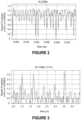
- FIGS. 2 and 3 which are waveform snippets of the signal envelopes typically observed in communications systems operating according to the Wideband Code Division Multiple Access (W-CDMA) air interface ( FIG. 2 ) and Long-Term Evolution (LTE) interface ( FIG. 3 ), the signal envelopes tend to fall to zero (or near zero) and inflect back from zero (or near zero) abruptly.
- W-CDMA Wideband Code Division Multiple Access
- LTE Long-Term Evolution
- US2018/0342991 describes a low wideband noise multi-stage switch-mode power amplifier.
- US2003/0160658 describes a power supply processing for power amplifiers.
- a wideband polar modulation transmitter is disclosed in accordance with the invention defined in the appended independent apparatus claim 1 and a method of increasing the bandwidth of a polar modulation transmitter is disclosed in accordance with the invention defined in appended independent method claim 8.
- the wideband polar modulation transmitter comprises a power amplifier (PA), a PA driver, a dynamic power supply (DPS), a PA driver V H controller, and a phase modulator.
- the phase modulator modulates a radio frequency (RF) carrier by an input phase modulating signal PM(t) to produce a phase modulated RF carrier.
- the DPS produces a DPS voltage for the PA that follows an input amplitude modulating signal AM(t).
- the PA driver uses the phase modulated RF carrier to generate a PA drive signal V DRV for driving the PA.
- the PA drive signal V DRV has a high drive level V H and a low drive level V L .
- the PA driver V H controller is configured to control the magnitude of the high drive level V H so that it remains sufficiently high to force the PA to operate in a compressed mode (C-mode) most of the time but lowers the high drive level V H to force the PA to operate in a product mode (P-mode) during times low-magnitude events occur in the DPS voltage.
- C-mode compressed mode
- P-mode product mode
- the polar modulation transmitter 400 comprises a power amplifier (PA) 402, a PA driver 404, a dynamic power supply (DPS) 406, a PA driver V H controller 408, and a phase modulator 410.
- PA power amplifier
- DPS dynamic power supply
- PA driver V H controller PA driver
- phase modulator 410 phase modulator
- the DPS 406 in the polar modulation transmitter 400 of the present invention modulates a direct current (DC) power supply voltage VDD2(DC) by an input amplitude modulating signal AM(t) to produce a dynamic power supply voltage VDD2(t), and the phase modulator 410 modulates an RF carrier by an input phase modulating signal PM(t) to produce a phase modulated RF carrier RF IN .
- DC direct current
- the polar modulation transmitter 400 further includes a PA driver 404 and a PA driver V H controller 408 that are designed and configured to drive the PA 402 so that it operates in compressed mode (i.e., "C-mode”) and, under certain conditions, alternatively in product mode (i.e., "P-mode").
- a PA driver 404 and a PA driver V H controller 408 that are designed and configured to drive the PA 402 so that it operates in compressed mode (i.e., "C-mode") and, under certain conditions, alternatively in product mode (i.e., "P-mode").
- the drive signal V DRV produced by the PA driver 404 has a low drive level V L and a high drive level V H .
- the PA driver V H controller 408 serves to control a driver power supply V DRV,SUPP for the PA driver 404, and the driver power supply V DRV,SUPP that is supplied determines what magnitude the high drive level V H is at any given time. Most of the time the PA driver V H controller 408 maintains the magnitude of the driver power supply V DRV,SUPP and high drive level V H at a magnitude sufficient to force the PA 404 to operate in C-mode, but lowers the high drive level V H to force the PA 404 to operate in P-mode during times low-magnitude events occur in the DPS voltage VDD2(t).
- low-magnitude events in the DPS voltage VDD2(t) are determined beforehand at baseband by a digital signal processor (DSP), i.e., before they appear in the DPS voltage VDD2(t), by monitoring the magnitude of the input amplitude modulating signal AM(t) (referred to as the "intended AM in the description that follows).
- DSP digital signal processor
- the DSP when the DSP determines that the magnitude of the intended AM has dropped below some predetermined C-mode / P-mode voltage threshold V C-P,TH , it directs the PA driver V H controller 408 to lower the power supply V DRV,SUPP so that the high drive level V H is lowered and so that the PA 404 will operate in P-mode when the low-magnitude event appears in the DPS voltage VDD2(t), and for the duration of the low-magnitude event.
- the Booth chart 500 shows how the RF output power P OUT produced by the PA 402 is influenced by variations in both the magnitude of the DPS voltage VDD2(t) and the magnitude of the RF input power applied to the RF input of the PA 402, when the PA 402 is configured for operation in three different operating modes - linear mode (i.e., "L-mode"), P-mode, and C-mode.
- Each curve in the Booth chart 500 represents a different power supply voltage VDD2 applied to the PA 402.
- the Booth chart 500 reveals that the RF output power P OUT produced by the PA 402 is sensitive to variations in the drain supply voltage VDD2 but not to variations in the RF input power.
- L-mode which is representative of a linear PA (e.g., a Class-A, B, or AB linear PA)
- the Booth chart 500 reveals that the RF output power P OUT produced by the PA 402 would be sensitive to variations in the RF input power but not to variations in the drain supply voltage VDD2.
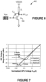
- the PA 402 comprises a power field-effect transistor (FET) 602 having a built-in parasitic gate-drain capacitor C gd , as illustrated in FIG. 6 .
- FET field-effect transistor
- This parasitic gate-drain capacitor C gd is undesirable since its serves as a leakage path through which the drive signal V DRV can undesirably leak from the RF input of the PA 402 (gate of the power FET) to the PA's 402's RF output RF OUT .
- L-mode operation is also responsive to variations in the gate drive voltage V GS (t) one might consider using L-mode to minimize gate-drain leakage, instead of P-mode.
- L-mode operation would require reconfiguring the PA 402 to operate as a linear PA, which is significantly less efficient compared to a PA operating in P-mode.
- L-mode operation also lacks the two degrees of freedom (V GS and VDD2) that P-mode has to reduce the output signal envelope to zero or near zero. For these reasons, P-mode operation is therefore preferred. Further details of P-mode operation and the various advantages it provides are discussed below. First, a more detailed description of C-mode operation is provided.
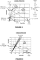
- FIG. 8 is plot showing the drain current I D versus drain-source voltage V DS characteristic curves of the PA's 402's power FET 602 and how the PA 402 operates when in C-mode, including how it performs drain modulation.
- C-mode operation is shown for two different DPS voltages VDD2(t 1 to t 2 ) and VDD2(t 3 to t 4 ) over two different time spans-a first time span t 1 ⁇ t ⁇ t 2 and a subsequent second time span t 3 ⁇ t ⁇ t 4 .
- the DPS 406 is supplying the first DPS voltage VDD2(t 1 to t 2 ).
- the drive signal V DRV is at its high drive level V H , thus causing the PA 402 to compress and switch fully ON.
- the drive signal V DRV drops to its low drive level V L , which is lower than the threshold voltage V T of the power FET 602, causing the PA 402 to enter the cut-off region of the I D v. V DS characteristic curves, i.e., to switch OFF.
- the PA 402 does not operate along the load line in the same sense that a linear PA operates along a load line. Instead, the PA 402 'snaps' between the compressed (ON) and cut-off (OFF) states, spending negligible time in between only during the very brief transitions between the two points. Subsequent to the first time span t 1 ⁇ t ⁇ t 2 and during the second time span t 3 ⁇ t ⁇ t 4 the DPS 406 is supplying the second DPS voltage VDD2(t 3 to t 4 ), where VDD2(t 3 to t 4 ) ⁇ VDD2(t 1 to t 2 ).
- the drive signal V DRV is at its high drive level V H , which causes the power PA 402 to once again compress and switch ON.
- the drive signal V DRV transitions to its low drive level V L , causing the PA 402 to enter the cut-off region and switch OFF.
- the RF output power P OUT produced by PA 402 depends on the square of the magnitude of the DPS voltage VDD2 2 (t), the RF output power P OUT (t 3 to t 4 ) during the second time span t 3 ⁇ t ⁇ t 4 is lower than the RF output power P OUT (t 1 to t 2 ) during the first time span t 1 ⁇ t ⁇ t 2 .
- FIG. 9 is a plot showing the drain current I D versus drain-source voltage V DS characteristic curves of the PA's 402's power FET 602, zooming in on the region of the characteristic curves involved during P-mode operation.
- the PA 402 When operating in P-mode, the PA 402 neither operates as a switch (as in C-mode) nor as a controlled current source (as in L-mode). Rather, in P-mode the PA 402 operates as what may be referred to as a "controlled variable resistance” (represented in FIG. 9 as an "effective" drain-source resistance R DS (eff)).
- the PA 402 is controlled to operate entirely in the triode region or entirely in the deep triode region.
- the group of V GS curves and their intersection with the load line 902 represents the values that the high drive level V H of the drive signal V DRV may have when the PA 402 is operating in P-mode during any given low-magnitude event.
- VDD2 (P-mode) ⁇ VDD2(t 3 to t 4 ) ⁇ VDD2(t 1 to t 2 ).
- VDD2 (P-mode) ⁇ VDD2(t 3 to t 4 ) ⁇ VDD2(t 1 to t 2 ).
- the magnitude of the high drive level V H (V GS (t) across the power FET 602) is reduced in accordance with each successive V GS curve following the direction of the arrow 904.
- Which of these values is used to drive the PA 402 is preferably determined at baseband by a digital signal processor (DSP), possibly taking into consideration predetermined leakage characteristics of the PA's 402's power FET 602. Further details concerning P-mode operation may be found in commonly owned U.S. Patent No. 9,397,713 , entitled “Polar Modulation Using Product Mode,”.
- DSP digital signal processor
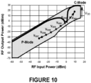
- the embellished Booth chart is presented here to further illustrate how the PA driver V H controller 408 and PA driver 404 work together during a transition from C-mode to P-mode.
- the PA driver V H controller 408 produces an output supply voltage V DRV,SUPP for the PA driver 404 that causes the PA driver 404 to produce a drive signal V DRV with a sufficiently high drive level V H to maintain the PA 402 in C-mode.
- the PA driver V H controller 408 begins to produce an output supply voltage V DRV,SUPP for the PA driver 404 that causes the PA driver 404 to produce a drive signal V DRV with a sufficiently high drive level V H to cause the PA 402 to compress and resume C-mode operation.
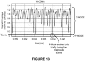
- the ability of the polar modulation transmitter 400 to control its PA 402 to operate in C-mode results in the polar modulation transmitter having high energy efficiency, and its ability to configure the PA 402 to operate in P-mode allows the signal envelope of its RF output RF OUT to reduce to zero or near zero when the intended AM dictates that it should.
- the ability to reproduce low-magnitude events in the RF output signal envelope is highlighted in the simplified drawing of the RF output voltage signal envelope depicted in FIG. 11 and compared to the inability of C-mode-only operation to reproduce similar low-magnitude events in FIG. 12 .
- FIG. 11 The ability to reproduce low-magnitude events in the RF output signal envelope is highlighted in the simplified drawing of the RF output voltage signal envelope depicted in FIG. 11 and compared to the inability of C-mode-only operation to reproduce similar low-magnitude events in FIG. 12 .
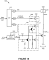
- FIG. 14 is a drawing depicting a polar modulation transmitter 1400 modeled after the polar modulation transmitter 400 described above, in accordance with one exemplary embodiment of the invention. Similar to the polar modulation transmitter 400 depicted in FIG. 4 , the polar modulation transmitter 1400 comprises a PA 1402, a PA driver 1404, a DPS 1406, a PA driver V H controller 1408, and a phase modulator 1410.
- the polar modulation transmitter 1400 also includes a DSP 1401 and digital-to-analog converters (DACs) 1403 that generate the analog amplitude and phase modulating signals AM(t) and PM(t) for the DPS 1406 and phase modulator 1410, and a PA driver V H control signal, which is applied to the gate of FET 1412 of the PA driver V H controller 1408, which in this exemplary embodiment of the invention comprises a source follower.
- DACs digital-to-analog converters
- the various FETs used in the PA 1402, PA driver 1404, and PA driver V H controller 1408 are all n-channel, depletion mode metal-semiconductor FETs (MESFETs) in this exemplary embodiment and, preferably, aluminum gallium nitride / gallium nitride (AlGaN/GaN) high electron mobility transistors (or "GaN-HEMTs"). Accordingly, in FIG. 14 the various FETs are depicted using the conventional n-channel, depletion mode transistor symbol commonly used for n-channel, depletion mode MESFETs.
- MESFETs depletion mode metal-semiconductor FETs
- the power FET 1405 in the PA 1402 could be some other compound semiconductor power FET or a silicon carbide power MOSFET, instead of a GaN-HEMT.
- the PA driver 1404 comprises a bootstrap Class-D driver, similar to as described in commonly owned U.S. Patent No. 9,806,678 , entitled “Bootstrap Class-D Wideband RF Power Amplifier,”, and comprises first, second, third and fourth FETs 1414, 1416, 1418 and 1420. Because the FETs in this exemplary embodiment of the invention are depletion mode FETs, i.e., "normally ON" FETs, their threshold voltages V T are negative. In the exemplary embodiment described here the threshold voltages V T are assumed to be the same for all four FETs 1414, 1416, 1418 and 1420.
- the "Class-D" property of the PA driver 1404 means that the first FET 1414 is switched ON when the second FET 1416 is switched OFF, and vice versa, and that the first and second FETs 1414 and 1416 are never ON at the same time, except perhaps during the very brief transitions between the first FET 1414 being switched ON and the second FET 1416 being switched OFF, and vice versa.
- the first FET 1414 is referred to as the "low-side FET” and the second FET 1416 is referred to as the "high-side FET.” Additionally, the third FET 1418 is referred to as the “control FET,” and the fourth FET 1420, which is configured to serve as a controlled resistor, is referred to as the "bootstrap resistor.”
- the phase modulated RF input signal RF IN produced by the phase modulator 1410 is AC coupled to both the gate of the low-side FET 1414 and gate of the control FET 1418, via DC blocking capacitors 1422 and 1424, and the gates of the low-side and control FETs 1414 and 1418 are biased by DC bias supply voltages V BIAS3 and V BIAS1 , to establish DC operating points V DC (1414) and V DC (1418) for the low-side and control FETs 1414 and 1418.
- V BIAS4 is set to 0V and V BIAS2 is set to some negative voltage less than, i.e., more negative than, V T .
- DC gate bias voltages V BIAS1 and V BIAS3 can be determined to establish the DC operating points V DC (1418) and V DC (1414) for the control FET 1418 and low-side FET 1414.
- the DC gate bias voltages V BIAS1 and V BIAS3 are set so that the gate voltage V G (1418) applied to the control FET 1418 swings between a high value of V BIAS2 and a low value of V T + V BIAS2 , as illustrated in FIG.
- the gate voltage V G (1414) applied to the low-side FET 1414 swings between a high value of 0V and a low value of less than V T , as illustrated in FIG. 15B .
- the gate-source voltage V GS (1418) applied across the gate-source terminals of the control FET 1418 and the gate-source voltage and V GS (1414) applied across the gate-source terminals of the low-side FET 1414 both swing between a high of 0V and a low value of V T , appropriate for switching the two FETs 1418 and 1414 ON and OFF.
- the control FET 1418 and low-side FET 1414 are switched ON and OFF under the direct control of the phase modulated RF input signal RF IN produced by the phase modulator 1410
- the high-side FET 1416 is switched ON and OFF by the coordinated control and operation of the low-side FET 1414, control FET 1418, and bootstrap resistor 1420.
- V G gate voltage
- V G gate voltage
- the gate voltages V G (1414) and V G (1418) applied to the gates of the low-side and control FETs 1414 and 1418 fall back down to the lower ends of their swings, the high-side FET 1416 is switched back ON, the control and low-side FETs 1418 and 1414 switch back OFF, and the bootstrap resistor 1420 bootstraps current from the RF output of the PA driver 1404 into the gate of the high-side FET 1416.
- the bootstrap current is initially supplied by the high-side FETs 1416's gate-source capacitor C gs , which was previously reverse-charged by V BIAS2 during the time the low-side and control FETs 1414 and 1418 were previously turned ON. However, shortly after the high-side FET 1416 begins turning ON and as the low-side FET 1414 is being turned OFF, current supplied from the PA driver's 1404's power supply VDD1 rapidly completes the forward charging of the gate-source capacitor C gs . Forward charging the gate-source capacitor C gs happens very rapidly and is completed on the order of picoseconds or less, depending on the resistance of the bootstrap resistor 1420 and the capacitance of the gate-source capacitor C gs .
- the supply VDD1 will supply additional current to the gate of the high-side FET 1416, via the bootstrap resistor 1420, in order to maintain the high-side FET 1416 in an ON state.
- This bootstrapping effect continues until the gate voltages V G (1414) and V G (1418) to the low-side and control FETs 1414 and 1418 once again increase to the upper ends of their swings and cause them to switch back ON.
- the gate-source capacitor C gs once again rapidly discharges through the control FET 1418 into the bias supply V BIAS2 , causing the high-side FET 1416 to turn back OFF.
- the PA driver V H controller 1408 in polar modulation transmitter 1400 comprises a source follower (i.e., common drain amplifier)
- the source follower 1408 has a high input impedance and a low output impedance and produces a driver supply voltage V DRV,SUPP that serves as the power supply for the PA driver 1404.
- the power supply voltage V DRV,SUPP is adjustable by the DSP 1401, depending on the magnitude of the input amplitude modulating signal AM(t), and establishes the upper rail voltage of the Class-D driver 1404.
- the source follower in addition to reducing the drive impedance to the driver-supply node and decreasing loading from the PA driver V H control input, the source follower also has the effect of increasing the bandwidth of the polar modulation transmitter 1400 through stronger current drive onto parasitic capacitances on the driver-supply node.
- the PA driver 1404 switches rail-to-rail and the adjustable power supply voltage V DRV
- SUPP supplied at the output of the source follower 1408 determines the high drive level V H of the drive signal V DRV applied to the PA 1402 the high drive level V H of magnitude at any give time determines whether the PA 1402 operates in C-mode or P-mode.
- the drive signal V DRV is AC coupled to the gate of the power FET 602 in the PA 402 and the gate of the power FET 602 is biased so that the low and high drive levels V L and V H of the drive signal V DRV are appropriate to switch the power FET 602 ON and OFF. In a preferred embodiment, however (depicted in FIG.
Landscapes
- Engineering & Computer Science (AREA)
- Power Engineering (AREA)
- Computer Networks & Wireless Communication (AREA)
- Signal Processing (AREA)
- Amplifiers (AREA)
Claims (10)
- Émetteur à modulation polaire, comprenant :une alimentation électrique dynamique, DPS, (406), qui génère et fournit, à une sortie DPS, une tension de DPS (VDD2(t)) présentant une amplitude qui suit un signal à modulation d'amplitude, AM, d'entrée (AM(t)) ;un modulateur de phase (410) qui module une porteuse radiofréquence, RF, (porteuse RF) par un signal à modulation de phase, PM, d'entrée (PM(t)) pour produire une porteuse RF modulée en phase (RFIN) ;un amplificateur électrique, PA, (402), comprenant un transistor à effet de champ, FET, électrique présentant un drain couplé à la sortie DPS, et configuré pour générer une sortie RF (RFOUT) ;un pilote de PA (40) qui génère un signal d'entraînement de PA (VDRV) à partir de la porteuse RF modulée en phase (RFIN), le signal d'entraînement de PA (VDRV) présentant un niveau d'entraînement élevé (VH) et un niveau d'entraînement faible (VL)un dispositif de commande VH de pilote de PA (408) qui commande une amplitude d'une tension d'alimentation électrique de pilote (VDRV,SUPP) fournie à une entrée d'alimentation de pilote du pilote de PA (404),dans lequel la tension d'alimentation électrique de pilote (VDRV,SUPP) détermine le niveau d'entraînement élevé (VH) du signal d'entraînement de PA (VDRV) produit par le pilote de PA (404), et le dispositif de commande VH de pilote de PA (408) est configuré pour maintenir l'amplitude de l'alimentation électrique de pilote (VDRV,SUPP) et le niveau d'entraînement élevé (VH) à une amplitude suffisante pour forcer le PA à fonctionner en mode compressé, mode C, et caractérisé en ce que le dispositif de commande VH de pilote de PA est en outre configuré pour abaisser l'alimentation électrique de pilote (VDRV,SUPP) et le niveau d'entraînement élevé (VH) pour forcer le PA à fonctionner en mode produit, mode P, pendant les moments où des événements de faible amplitude sont présents dans la tension de DPS (VDD2(t)) ; etdans lequel, lorsque le PA fonctionne en mode P, la sortie RF (RFOUT) du PA est proportionnelle au produit de l'amplitude de la tension de DPS (VDD2(t)) et de l'amplitude de la tension du signal d'entraînement de PA (VDRV).
- Émetteur à modulation polaire selon la revendication 1, dans lequel le pilote de PA comprend un amplificateur de classe D.
- Émetteur à modulation polaire selon la revendication 1, dans lequel le dispositif de commande VH de pilote de PA comprend un suiveur de source.
- Émetteur à modulation polaire selon la revendication 1, dans lequel le signal d'entraînement de PA (VDRV) généré par le pilote de PA est couplé en courant continu à une grille du FET électrique du PA.
- Émetteur à modulation polaire selon la revendication 1, comprenant en outre un processeur de signal numérique, DSP, configuré pour :déterminer quand les événements de faible amplitude se produiront dans la tension de DPS ; etordonner au dispositif de commande VH de pilote de PA de réduire la tension d'alimentation électrique de pilote (VDRV,SUPP) et le niveau d'entraînement élevé (VH) du signal d'entraînement de PA (VDRV) lorsque les événements de faible amplitude se produisent dans la tension de DPS, le PA est forcé de fonctionner en mode P pendant les durées des événements de faible amplitude.
- Émetteur à modulation polaire selon la revendication 5, dans lequel le DSP est configuré pour surveiller le signal à modulation d'amplitude d'entrée pour déterminer quand les événements de faible amplitude se produiront dans la tension de DPS.
- Émetteur à modulation polaire selon la revendication 6, dans lequel le DSP est configuré pour déterminer que les événements de faible amplitude se produiront dans la tension de DPS lorsque l'amplitude du signal à modulation d'amplitude d'entrée tombe en dessous d'un seuil de tension en mode C/mode P prédéterminé.
- Procédé d'augmentation de la bande passante d'un émetteur à modulation polaire, comprenant les étapes consistant à :générer une tension d'alimentation électrique dynamique, DPS, qui suit un signal à modulation d'amplitude d'entrée ;coupler la tension de DPS à une entrée d'alimentation électrique d'un amplificateur électrique, PA, configuré pour générer une sortie RF (RFOUT) ;générer un signal d'entraînement de PA (VDRV) présentant un niveau d'entraînement élevé (VH) et un niveau d'entraînement faible (VL) à une sortie d'un pilote de PA ;entraîner le PA par l'intermédiaire du signal d'entraînement de PA (VDRV) ;générer un signal de commande de tension d'alimentation électrique de dispositif d'entraînement ; etappliquer le signal d'entraînement de tension d'alimentation électrique de pilote à une entrée d'un suiveur de source dont la source est couplée à une entrée d'alimentation électrique du pilote de PA,dans lequel le niveau d'entraînement élevé (VH) du signal d'entraînement de PA (VDRV) est déterminé par le signal d'entraînement de tension d'alimentation électrique du pilote et le signal de commande de tension d'alimentation électrique de pilote est maintenu à une valeur qui fait fonctionner le PA en mode compressé, mode C, la plupart du temps,et dans lequel le procédé est caractérisé en ce que le signal d'entraînement de tension d'alimentation électrique de pilote est ajusté pour amener le PA à fonctionner en mode produit, mode P, pendant les moments où des événements de faible amplitude se produisent dans la tension de DPS ; etdans lequel, lorsque le PA fonctionne en mode P, la sortie RF (RFOUT) du PA est proportionnelle au produit de l'amplitude de la tension de DPS et de l'amplitude de la tension du signal d'entraînement de PA (VDRV).
- Procédé selon la revendication 8, comprenant en outre les étapes consistant à :surveiller une amplitude du signal à modulation d'amplitude d'entrée pour déterminer quand un événement de faible amplitude se produira dans la tension de DPS ; etajuster le signal d'entraînement de tension d'alimentation de pilote de telle sorte que lorsque l'événement de faible amplitude se produit dans la tension de DPS, le niveau d'entraînement élevé (VH) du signal d'entraînement de PA (VDRV) est maintenu à un niveau ou à des niveaux qui forcent le PA à fonctionner en mode P pendant la durée de l'événement de faible amplitude.
- Procédé selon la revendication 9, comprenant en outre les étapes consistant à :comparer l'amplitude surveillée du signal à modulation d'amplitude d'entrée à un seuil de tension en mode C/mode P (VC-P,TH) ;déterminer qu'un événement de faible amplitude se produira dans la tension de DPS si l'amplitude du signal à modulation d'amplitude d'entrée tombe en dessous du seuil de tension en mode C/mode P (VC-P,TH) ; etajuster le signal d'entraînement de la tension d'alimentation électrique de pilote de sorte que lorsque l'événement de faible amplitude se produit dans la tension de DPS, le niveau d'entraînement élevé (VH) du signal d'entraînement de PA (VRDV) est maintenu à un niveau ou à des niveaux qui forcent le PA à fonctionner en mode P pendant la durée de l'événement de faible magnitude.
Applications Claiming Priority (2)
| Application Number | Priority Date | Filing Date | Title |
|---|---|---|---|
| US16/539,844 US10735034B1 (en) | 2019-08-13 | 2019-08-13 | Polar modulation transmitter with wideband product mode control |
| PCT/US2020/039533 WO2021029974A1 (fr) | 2019-08-13 | 2020-06-25 | Émetteur à modulation polaire avec commande de mode de produit à large bande |
Publications (4)
| Publication Number | Publication Date |
|---|---|
| EP4014323A1 EP4014323A1 (fr) | 2022-06-22 |
| EP4014323A4 EP4014323A4 (fr) | 2023-09-13 |
| EP4014323B1 true EP4014323B1 (fr) | 2024-08-21 |
| EP4014323C0 EP4014323C0 (fr) | 2024-08-21 |
Family
ID=71838762
Family Applications (1)
| Application Number | Title | Priority Date | Filing Date |
|---|---|---|---|
| EP20853444.6A Active EP4014323B1 (fr) | 2019-08-13 | 2020-06-25 | Émetteur à modulation polaire avec commande de mode de produit à large bande |
Country Status (4)
| Country | Link |
|---|---|
| US (1) | US10735034B1 (fr) |
| EP (1) | EP4014323B1 (fr) |
| CN (1) | CN114467261B (fr) |
| WO (1) | WO2021029974A1 (fr) |
Family Cites Families (11)
| Publication number | Priority date | Publication date | Assignee | Title |
|---|---|---|---|---|
| CN1249912C (zh) * | 1999-07-29 | 2006-04-05 | 特罗皮亚恩公司 | 高效调制射频放大器 |
| US6781452B2 (en) * | 2001-08-29 | 2004-08-24 | Tropian, Inc. | Power supply processing for power amplifiers |
| CN101416400A (zh) * | 2006-03-30 | 2009-04-22 | Nxp股份有限公司 | 多模式无线电发射机及其操作方法 |
| US7783269B2 (en) * | 2007-09-20 | 2010-08-24 | Quantance, Inc. | Power amplifier controller with polar transmitter |
| US8301088B2 (en) * | 2007-10-26 | 2012-10-30 | Panasonic Corporation | Polar modulation transmitter with envelope modulator path switching |
| US20100009641A1 (en) * | 2008-07-11 | 2010-01-14 | Matsushita Electric Industrial Co.,Ltd. | Digital rf phase control in polar modulation transmitters |
| US8270916B2 (en) * | 2009-01-09 | 2012-09-18 | Panasonic Corporation | Methods for tuning and controlling output power in polar transmitters |
| US9397621B2 (en) * | 2014-07-30 | 2016-07-19 | Eridan Communications, Inc. | Limiting driver for switch-mode power amplifier |
| US9806678B2 (en) * | 2015-06-29 | 2017-10-31 | Eridan Communications, Inc. | Bootstrap class-D wideband RF power amplifier |
| US9397713B1 (en) * | 2015-12-03 | 2016-07-19 | Eridan Communications, Inc. | Polar modulation using product mode |
| US10680563B2 (en) | 2017-05-23 | 2020-06-09 | Eridan Communications, Inc. | Low wideband noise multi-stage switch-mode power amplifier |
-
2019
- 2019-08-13 US US16/539,844 patent/US10735034B1/en active Active
-
2020
- 2020-06-25 WO PCT/US2020/039533 patent/WO2021029974A1/fr not_active Ceased
- 2020-06-25 CN CN202080056952.9A patent/CN114467261B/zh active Active
- 2020-06-25 EP EP20853444.6A patent/EP4014323B1/fr active Active
Also Published As
| Publication number | Publication date |
|---|---|
| EP4014323A4 (fr) | 2023-09-13 |
| CN114467261B (zh) | 2023-03-31 |
| EP4014323A1 (fr) | 2022-06-22 |
| US10735034B1 (en) | 2020-08-04 |
| WO2021029974A1 (fr) | 2021-02-18 |
| EP4014323C0 (fr) | 2024-08-21 |
| CN114467261A (zh) | 2022-05-10 |
Similar Documents
| Publication | Publication Date | Title |
|---|---|---|
| US6566944B1 (en) | Current modulator with dynamic amplifier impedance compensation | |
| US5838193A (en) | Time-delay compensating wideband class-s modulator and method therefor | |
| US7728662B2 (en) | Saturated power amplifier with selectable and variable output power levels | |
| US6072361A (en) | Wideband class-S modulator and method therefor | |
| CN112236938B (zh) | 电源调制器、具有其的功率放大器和对应的控制方法 | |
| US9899970B2 (en) | Current enhanced driver for high-power solid-state radio frequency power amplifiers | |
| US20050057308A1 (en) | Method and apparatus for dynamically regulating the supply voltage of a power amplifier | |
| EP3607653B1 (fr) | Modulation polaire utilisant un mode de produit | |
| US9455670B2 (en) | Scalable periphery for digital power control | |
| US20170019069A1 (en) | High-Speed, High-Voltage GaN-Based Operational Amplifier | |
| US10680563B2 (en) | Low wideband noise multi-stage switch-mode power amplifier | |
| US8364099B2 (en) | Methods and apparatus for controlling leakage and power dissipation in radio frequency power amplifiers | |
| US6498533B1 (en) | Bootstrapped dual-gate class E amplifier circuit | |
| US10608592B2 (en) | Linear amplifier having higher efficiency for envelope tracking modulator | |
| US11539329B2 (en) | Wideband envelope control in polar modulators | |
| EP4014323B1 (fr) | Émetteur à modulation polaire avec commande de mode de produit à large bande | |
| JP2672731B2 (ja) | 電力増幅回路 | |
| US7426372B2 (en) | Piecewise linearizer circuit for radio frequency amplification | |
| US20060091956A1 (en) | Amplifying a signal using a control modulator that provides a bias resistance |
Legal Events
| Date | Code | Title | Description |
|---|---|---|---|
| STAA | Information on the status of an ep patent application or granted ep patent |
Free format text: STATUS: THE INTERNATIONAL PUBLICATION HAS BEEN MADE |
|
| PUAI | Public reference made under article 153(3) epc to a published international application that has entered the european phase |
Free format text: ORIGINAL CODE: 0009012 |
|
| STAA | Information on the status of an ep patent application or granted ep patent |
Free format text: STATUS: REQUEST FOR EXAMINATION WAS MADE |
|
| 17P | Request for examination filed |
Effective date: 20220204 |
|
| AK | Designated contracting states |
Kind code of ref document: A1 Designated state(s): AL AT BE BG CH CY CZ DE DK EE ES FI FR GB GR HR HU IE IS IT LI LT LU LV MC MK MT NL NO PL PT RO RS SE SI SK SM TR |
|
| DAV | Request for validation of the european patent (deleted) | ||
| DAX | Request for extension of the european patent (deleted) | ||
| RAP3 | Party data changed (applicant data changed or rights of an application transferred) |
Owner name: ERIDAN COMMUNICATIONS, INC. |
|
| RIN1 | Information on inventor provided before grant (corrected) |
Inventor name: DIDUCK, QUENTIN |
|
| A4 | Supplementary search report drawn up and despatched |
Effective date: 20230810 |
|
| RIC1 | Information provided on ipc code assigned before grant |
Ipc: H04L 27/36 20060101ALI20230804BHEP Ipc: H03F 3/21 20060101ALI20230804BHEP Ipc: H03F 3/193 20060101ALI20230804BHEP Ipc: H03F 3/217 20060101ALI20230804BHEP Ipc: H03F 1/42 20060101ALI20230804BHEP Ipc: H04L 27/12 20060101ALI20230804BHEP Ipc: H03F 3/24 20060101ALI20230804BHEP Ipc: H03F 1/02 20060101ALI20230804BHEP Ipc: H03C 3/18 20060101ALI20230804BHEP Ipc: H03C 3/02 20060101ALI20230804BHEP Ipc: H04B 1/04 20060101AFI20230804BHEP |
|
| GRAP | Despatch of communication of intention to grant a patent |
Free format text: ORIGINAL CODE: EPIDOSNIGR1 |
|
| STAA | Information on the status of an ep patent application or granted ep patent |
Free format text: STATUS: GRANT OF PATENT IS INTENDED |
|
| INTG | Intention to grant announced |
Effective date: 20240422 |
|
| GRAS | Grant fee paid |
Free format text: ORIGINAL CODE: EPIDOSNIGR3 |
|
| GRAA | (expected) grant |
Free format text: ORIGINAL CODE: 0009210 |
|
| STAA | Information on the status of an ep patent application or granted ep patent |
Free format text: STATUS: THE PATENT HAS BEEN GRANTED |
|
| AK | Designated contracting states |
Kind code of ref document: B1 Designated state(s): AL AT BE BG CH CY CZ DE DK EE ES FI FR GB GR HR HU IE IS IT LI LT LU LV MC MK MT NL NO PL PT RO RS SE SI SK SM TR |
|
| REG | Reference to a national code |
Ref country code: GB Ref legal event code: FG4D |
|
| REG | Reference to a national code |
Ref country code: CH Ref legal event code: EP |
|
| REG | Reference to a national code |
Ref country code: DE Ref legal event code: R096 Ref document number: 602020036400 Country of ref document: DE |
|
| REG | Reference to a national code |
Ref country code: IE Ref legal event code: FG4D |
|
| U01 | Request for unitary effect filed |
Effective date: 20240828 |
|
| U07 | Unitary effect registered |
Designated state(s): AT BE BG DE DK EE FI FR IT LT LU LV MT NL PT RO SE SI Effective date: 20240909 |
|
| PG25 | Lapsed in a contracting state [announced via postgrant information from national office to epo] |
Ref country code: NO Free format text: LAPSE BECAUSE OF FAILURE TO SUBMIT A TRANSLATION OF THE DESCRIPTION OR TO PAY THE FEE WITHIN THE PRESCRIBED TIME-LIMIT Effective date: 20241121 |
|
| PG25 | Lapsed in a contracting state [announced via postgrant information from national office to epo] |
Ref country code: GR Free format text: LAPSE BECAUSE OF FAILURE TO SUBMIT A TRANSLATION OF THE DESCRIPTION OR TO PAY THE FEE WITHIN THE PRESCRIBED TIME-LIMIT Effective date: 20241122 Ref country code: PL Free format text: LAPSE BECAUSE OF FAILURE TO SUBMIT A TRANSLATION OF THE DESCRIPTION OR TO PAY THE FEE WITHIN THE PRESCRIBED TIME-LIMIT Effective date: 20240821 |
|
| PG25 | Lapsed in a contracting state [announced via postgrant information from national office to epo] |
Ref country code: IS Free format text: LAPSE BECAUSE OF FAILURE TO SUBMIT A TRANSLATION OF THE DESCRIPTION OR TO PAY THE FEE WITHIN THE PRESCRIBED TIME-LIMIT Effective date: 20241221 |
|
| PG25 | Lapsed in a contracting state [announced via postgrant information from national office to epo] |
Ref country code: HR Free format text: LAPSE BECAUSE OF FAILURE TO SUBMIT A TRANSLATION OF THE DESCRIPTION OR TO PAY THE FEE WITHIN THE PRESCRIBED TIME-LIMIT Effective date: 20240821 |
|
| PG25 | Lapsed in a contracting state [announced via postgrant information from national office to epo] |
Ref country code: ES Free format text: LAPSE BECAUSE OF FAILURE TO SUBMIT A TRANSLATION OF THE DESCRIPTION OR TO PAY THE FEE WITHIN THE PRESCRIBED TIME-LIMIT Effective date: 20240821 Ref country code: RS Free format text: LAPSE BECAUSE OF FAILURE TO SUBMIT A TRANSLATION OF THE DESCRIPTION OR TO PAY THE FEE WITHIN THE PRESCRIBED TIME-LIMIT Effective date: 20241121 |
|
| PG25 | Lapsed in a contracting state [announced via postgrant information from national office to epo] |
Ref country code: RS Free format text: LAPSE BECAUSE OF FAILURE TO SUBMIT A TRANSLATION OF THE DESCRIPTION OR TO PAY THE FEE WITHIN THE PRESCRIBED TIME-LIMIT Effective date: 20241121 Ref country code: PL Free format text: LAPSE BECAUSE OF FAILURE TO SUBMIT A TRANSLATION OF THE DESCRIPTION OR TO PAY THE FEE WITHIN THE PRESCRIBED TIME-LIMIT Effective date: 20240821 Ref country code: NO Free format text: LAPSE BECAUSE OF FAILURE TO SUBMIT A TRANSLATION OF THE DESCRIPTION OR TO PAY THE FEE WITHIN THE PRESCRIBED TIME-LIMIT Effective date: 20241121 Ref country code: IS Free format text: LAPSE BECAUSE OF FAILURE TO SUBMIT A TRANSLATION OF THE DESCRIPTION OR TO PAY THE FEE WITHIN THE PRESCRIBED TIME-LIMIT Effective date: 20241221 Ref country code: HR Free format text: LAPSE BECAUSE OF FAILURE TO SUBMIT A TRANSLATION OF THE DESCRIPTION OR TO PAY THE FEE WITHIN THE PRESCRIBED TIME-LIMIT Effective date: 20240821 Ref country code: GR Free format text: LAPSE BECAUSE OF FAILURE TO SUBMIT A TRANSLATION OF THE DESCRIPTION OR TO PAY THE FEE WITHIN THE PRESCRIBED TIME-LIMIT Effective date: 20241122 Ref country code: ES Free format text: LAPSE BECAUSE OF FAILURE TO SUBMIT A TRANSLATION OF THE DESCRIPTION OR TO PAY THE FEE WITHIN THE PRESCRIBED TIME-LIMIT Effective date: 20240821 |
|
| PG25 | Lapsed in a contracting state [announced via postgrant information from national office to epo] |
Ref country code: SM Free format text: LAPSE BECAUSE OF FAILURE TO SUBMIT A TRANSLATION OF THE DESCRIPTION OR TO PAY THE FEE WITHIN THE PRESCRIBED TIME-LIMIT Effective date: 20240821 |
|
| PG25 | Lapsed in a contracting state [announced via postgrant information from national office to epo] |
Ref country code: CZ Free format text: LAPSE BECAUSE OF FAILURE TO SUBMIT A TRANSLATION OF THE DESCRIPTION OR TO PAY THE FEE WITHIN THE PRESCRIBED TIME-LIMIT Effective date: 20240821 |
|
| PG25 | Lapsed in a contracting state [announced via postgrant information from national office to epo] |
Ref country code: SK Free format text: LAPSE BECAUSE OF FAILURE TO SUBMIT A TRANSLATION OF THE DESCRIPTION OR TO PAY THE FEE WITHIN THE PRESCRIBED TIME-LIMIT Effective date: 20240821 |
|
| PLBE | No opposition filed within time limit |
Free format text: ORIGINAL CODE: 0009261 |
|
| STAA | Information on the status of an ep patent application or granted ep patent |
Free format text: STATUS: NO OPPOSITION FILED WITHIN TIME LIMIT |
|
| PGFP | Annual fee paid to national office [announced via postgrant information from national office to epo] |
Ref country code: GB Payment date: 20250523 Year of fee payment: 6 |
|
| U20 | Renewal fee for the european patent with unitary effect paid |
Year of fee payment: 6 Effective date: 20250617 |
|
| 26N | No opposition filed |
Effective date: 20250522 |
|
| REG | Reference to a national code |
Ref country code: CH Ref legal event code: H13 Free format text: ST27 STATUS EVENT CODE: U-0-0-H10-H13 (AS PROVIDED BY THE NATIONAL OFFICE) Effective date: 20260127 |
|
| PG25 | Lapsed in a contracting state [announced via postgrant information from national office to epo] |
Ref country code: MC Free format text: LAPSE BECAUSE OF FAILURE TO SUBMIT A TRANSLATION OF THE DESCRIPTION OR TO PAY THE FEE WITHIN THE PRESCRIBED TIME-LIMIT Effective date: 20240821 |
|
| PG25 | Lapsed in a contracting state [announced via postgrant information from national office to epo] |
Ref country code: IE Free format text: LAPSE BECAUSE OF NON-PAYMENT OF DUE FEES Effective date: 20250625 |
|
| PG25 | Lapsed in a contracting state [announced via postgrant information from national office to epo] |
Ref country code: CH Free format text: LAPSE BECAUSE OF NON-PAYMENT OF DUE FEES Effective date: 20250630 |