EP4016513A1 - Appareil d'affichage et dispositif électronique - Google Patents
Appareil d'affichage et dispositif électronique Download PDFInfo
- Publication number
- EP4016513A1 EP4016513A1 EP20882197.5A EP20882197A EP4016513A1 EP 4016513 A1 EP4016513 A1 EP 4016513A1 EP 20882197 A EP20882197 A EP 20882197A EP 4016513 A1 EP4016513 A1 EP 4016513A1
- Authority
- EP
- European Patent Office
- Prior art keywords
- display area
- pixels
- display
- driving units
- display device
- Prior art date
- Legal status (The legal status is an assumption and is not a legal conclusion. Google has not performed a legal analysis and makes no representation as to the accuracy of the status listed.)
- Withdrawn
Links
- 239000000758 substrate Substances 0.000 claims description 29
- 238000000034 method Methods 0.000 claims description 15
- 239000003086 colorant Substances 0.000 claims description 8
- 230000003287 optical effect Effects 0.000 claims description 3
- 238000002834 transmittance Methods 0.000 abstract description 27
- 238000010586 diagram Methods 0.000 description 28
- 239000010409 thin film Substances 0.000 description 10
- 230000000694 effects Effects 0.000 description 7
- 239000000463 material Substances 0.000 description 5
- 239000011521 glass Substances 0.000 description 4
- 238000003384 imaging method Methods 0.000 description 4
- 230000007704 transition Effects 0.000 description 4
- 229920001621 AMOLED Polymers 0.000 description 3
- 230000005540 biological transmission Effects 0.000 description 3
- 230000008054 signal transmission Effects 0.000 description 3
- 238000011161 development Methods 0.000 description 2
- 238000005516 engineering process Methods 0.000 description 2
- 239000004033 plastic Substances 0.000 description 2
- 229910052782 aluminium Inorganic materials 0.000 description 1
- XAGFODPZIPBFFR-UHFFFAOYSA-N aluminium Chemical compound [Al] XAGFODPZIPBFFR-UHFFFAOYSA-N 0.000 description 1
- 239000003990 capacitor Substances 0.000 description 1
- 239000000919 ceramic Substances 0.000 description 1
- 238000004140 cleaning Methods 0.000 description 1
- 238000004891 communication Methods 0.000 description 1
- 239000002131 composite material Substances 0.000 description 1
- 238000013461 design Methods 0.000 description 1
- 230000006866 deterioration Effects 0.000 description 1
- 239000000835 fiber Substances 0.000 description 1
- 230000001788 irregular Effects 0.000 description 1
- 239000011159 matrix material Substances 0.000 description 1
- 229910052751 metal Inorganic materials 0.000 description 1
- 239000002184 metal Substances 0.000 description 1
- 238000012986 modification Methods 0.000 description 1
- 230000004048 modification Effects 0.000 description 1
- 238000012545 processing Methods 0.000 description 1
- 229910052594 sapphire Inorganic materials 0.000 description 1
- 239000010980 sapphire Substances 0.000 description 1
- 229910001220 stainless steel Inorganic materials 0.000 description 1
- 239000010935 stainless steel Substances 0.000 description 1
- 239000012780 transparent material Substances 0.000 description 1
- 210000000707 wrist Anatomy 0.000 description 1
Images




Classifications
-
- G—PHYSICS
- G09—EDUCATION; CRYPTOGRAPHY; DISPLAY; ADVERTISING; SEALS
- G09G—ARRANGEMENTS OR CIRCUITS FOR CONTROL OF INDICATING DEVICES USING STATIC MEANS TO PRESENT VARIABLE INFORMATION
- G09G3/00—Control arrangements or circuits, of interest only in connection with visual indicators other than cathode-ray tubes
- G09G3/20—Control arrangements or circuits, of interest only in connection with visual indicators other than cathode-ray tubes for presentation of an assembly of a number of characters, e.g. a page, by composing the assembly by combination of individual elements arranged in a matrix no fixed position being assigned to or needed to be assigned to the individual characters or partial characters
- G09G3/22—Control arrangements or circuits, of interest only in connection with visual indicators other than cathode-ray tubes for presentation of an assembly of a number of characters, e.g. a page, by composing the assembly by combination of individual elements arranged in a matrix no fixed position being assigned to or needed to be assigned to the individual characters or partial characters using controlled light sources
- G09G3/30—Control arrangements or circuits, of interest only in connection with visual indicators other than cathode-ray tubes for presentation of an assembly of a number of characters, e.g. a page, by composing the assembly by combination of individual elements arranged in a matrix no fixed position being assigned to or needed to be assigned to the individual characters or partial characters using controlled light sources using electroluminescent panels
- G09G3/32—Control arrangements or circuits, of interest only in connection with visual indicators other than cathode-ray tubes for presentation of an assembly of a number of characters, e.g. a page, by composing the assembly by combination of individual elements arranged in a matrix no fixed position being assigned to or needed to be assigned to the individual characters or partial characters using controlled light sources using electroluminescent panels semiconductive, e.g. using light-emitting diodes [LED]
- G09G3/3208—Control arrangements or circuits, of interest only in connection with visual indicators other than cathode-ray tubes for presentation of an assembly of a number of characters, e.g. a page, by composing the assembly by combination of individual elements arranged in a matrix no fixed position being assigned to or needed to be assigned to the individual characters or partial characters using controlled light sources using electroluminescent panels semiconductive, e.g. using light-emitting diodes [LED] organic, e.g. using organic light-emitting diodes [OLED]
-
- G—PHYSICS
- G09—EDUCATION; CRYPTOGRAPHY; DISPLAY; ADVERTISING; SEALS
- G09G—ARRANGEMENTS OR CIRCUITS FOR CONTROL OF INDICATING DEVICES USING STATIC MEANS TO PRESENT VARIABLE INFORMATION
- G09G3/00—Control arrangements or circuits, of interest only in connection with visual indicators other than cathode-ray tubes
- G09G3/20—Control arrangements or circuits, of interest only in connection with visual indicators other than cathode-ray tubes for presentation of an assembly of a number of characters, e.g. a page, by composing the assembly by combination of individual elements arranged in a matrix no fixed position being assigned to or needed to be assigned to the individual characters or partial characters
- G09G3/22—Control arrangements or circuits, of interest only in connection with visual indicators other than cathode-ray tubes for presentation of an assembly of a number of characters, e.g. a page, by composing the assembly by combination of individual elements arranged in a matrix no fixed position being assigned to or needed to be assigned to the individual characters or partial characters using controlled light sources
- G09G3/30—Control arrangements or circuits, of interest only in connection with visual indicators other than cathode-ray tubes for presentation of an assembly of a number of characters, e.g. a page, by composing the assembly by combination of individual elements arranged in a matrix no fixed position being assigned to or needed to be assigned to the individual characters or partial characters using controlled light sources using electroluminescent panels
- G09G3/32—Control arrangements or circuits, of interest only in connection with visual indicators other than cathode-ray tubes for presentation of an assembly of a number of characters, e.g. a page, by composing the assembly by combination of individual elements arranged in a matrix no fixed position being assigned to or needed to be assigned to the individual characters or partial characters using controlled light sources using electroluminescent panels semiconductive, e.g. using light-emitting diodes [LED]
- G09G3/3208—Control arrangements or circuits, of interest only in connection with visual indicators other than cathode-ray tubes for presentation of an assembly of a number of characters, e.g. a page, by composing the assembly by combination of individual elements arranged in a matrix no fixed position being assigned to or needed to be assigned to the individual characters or partial characters using controlled light sources using electroluminescent panels semiconductive, e.g. using light-emitting diodes [LED] organic, e.g. using organic light-emitting diodes [OLED]
- G09G3/3216—Control arrangements or circuits, of interest only in connection with visual indicators other than cathode-ray tubes for presentation of an assembly of a number of characters, e.g. a page, by composing the assembly by combination of individual elements arranged in a matrix no fixed position being assigned to or needed to be assigned to the individual characters or partial characters using controlled light sources using electroluminescent panels semiconductive, e.g. using light-emitting diodes [LED] organic, e.g. using organic light-emitting diodes [OLED] using a passive matrix
-
- G—PHYSICS
- G09—EDUCATION; CRYPTOGRAPHY; DISPLAY; ADVERTISING; SEALS
- G09G—ARRANGEMENTS OR CIRCUITS FOR CONTROL OF INDICATING DEVICES USING STATIC MEANS TO PRESENT VARIABLE INFORMATION
- G09G3/00—Control arrangements or circuits, of interest only in connection with visual indicators other than cathode-ray tubes
- G09G3/20—Control arrangements or circuits, of interest only in connection with visual indicators other than cathode-ray tubes for presentation of an assembly of a number of characters, e.g. a page, by composing the assembly by combination of individual elements arranged in a matrix no fixed position being assigned to or needed to be assigned to the individual characters or partial characters
- G09G3/22—Control arrangements or circuits, of interest only in connection with visual indicators other than cathode-ray tubes for presentation of an assembly of a number of characters, e.g. a page, by composing the assembly by combination of individual elements arranged in a matrix no fixed position being assigned to or needed to be assigned to the individual characters or partial characters using controlled light sources
- G09G3/30—Control arrangements or circuits, of interest only in connection with visual indicators other than cathode-ray tubes for presentation of an assembly of a number of characters, e.g. a page, by composing the assembly by combination of individual elements arranged in a matrix no fixed position being assigned to or needed to be assigned to the individual characters or partial characters using controlled light sources using electroluminescent panels
- G09G3/32—Control arrangements or circuits, of interest only in connection with visual indicators other than cathode-ray tubes for presentation of an assembly of a number of characters, e.g. a page, by composing the assembly by combination of individual elements arranged in a matrix no fixed position being assigned to or needed to be assigned to the individual characters or partial characters using controlled light sources using electroluminescent panels semiconductive, e.g. using light-emitting diodes [LED]
- G09G3/3208—Control arrangements or circuits, of interest only in connection with visual indicators other than cathode-ray tubes for presentation of an assembly of a number of characters, e.g. a page, by composing the assembly by combination of individual elements arranged in a matrix no fixed position being assigned to or needed to be assigned to the individual characters or partial characters using controlled light sources using electroluminescent panels semiconductive, e.g. using light-emitting diodes [LED] organic, e.g. using organic light-emitting diodes [OLED]
- G09G3/3225—Control arrangements or circuits, of interest only in connection with visual indicators other than cathode-ray tubes for presentation of an assembly of a number of characters, e.g. a page, by composing the assembly by combination of individual elements arranged in a matrix no fixed position being assigned to or needed to be assigned to the individual characters or partial characters using controlled light sources using electroluminescent panels semiconductive, e.g. using light-emitting diodes [LED] organic, e.g. using organic light-emitting diodes [OLED] using an active matrix
-
- H—ELECTRICITY
- H10—SEMICONDUCTOR DEVICES; ELECTRIC SOLID-STATE DEVICES NOT OTHERWISE PROVIDED FOR
- H10K—ORGANIC ELECTRIC SOLID-STATE DEVICES
- H10K59/00—Integrated devices, or assemblies of multiple devices, comprising at least one organic light-emitting element covered by group H10K50/00
- H10K59/10—OLED displays
- H10K59/12—Active-matrix OLED [AMOLED] displays
- H10K59/121—Active-matrix OLED [AMOLED] displays characterised by the geometry or disposition of pixel elements
-
- H—ELECTRICITY
- H10—SEMICONDUCTOR DEVICES; ELECTRIC SOLID-STATE DEVICES NOT OTHERWISE PROVIDED FOR
- H10K—ORGANIC ELECTRIC SOLID-STATE DEVICES
- H10K59/00—Integrated devices, or assemblies of multiple devices, comprising at least one organic light-emitting element covered by group H10K50/00
- H10K59/80—Constructional details
- H10K59/84—Parallel electrical configurations of multiple OLEDs
-
- G—PHYSICS
- G09—EDUCATION; CRYPTOGRAPHY; DISPLAY; ADVERTISING; SEALS
- G09G—ARRANGEMENTS OR CIRCUITS FOR CONTROL OF INDICATING DEVICES USING STATIC MEANS TO PRESENT VARIABLE INFORMATION
- G09G2300/00—Aspects of the constitution of display devices
- G09G2300/04—Structural and physical details of display devices
- G09G2300/0421—Structural details of the set of electrodes
- G09G2300/0426—Layout of electrodes and connections
-
- G—PHYSICS
- G09—EDUCATION; CRYPTOGRAPHY; DISPLAY; ADVERTISING; SEALS
- G09G—ARRANGEMENTS OR CIRCUITS FOR CONTROL OF INDICATING DEVICES USING STATIC MEANS TO PRESENT VARIABLE INFORMATION
- G09G2300/00—Aspects of the constitution of display devices
- G09G2300/04—Structural and physical details of display devices
- G09G2300/0439—Pixel structures
- G09G2300/0452—Details of colour pixel setup, e.g. pixel composed of a red, a blue and two green components
-
- G—PHYSICS
- G09—EDUCATION; CRYPTOGRAPHY; DISPLAY; ADVERTISING; SEALS
- G09G—ARRANGEMENTS OR CIRCUITS FOR CONTROL OF INDICATING DEVICES USING STATIC MEANS TO PRESENT VARIABLE INFORMATION
- G09G2300/00—Aspects of the constitution of display devices
- G09G2300/04—Structural and physical details of display devices
- G09G2300/0439—Pixel structures
- G09G2300/0465—Improved aperture ratio, e.g. by size reduction of the pixel circuit, e.g. for improving the pixel density or the maximum displayable luminance or brightness
-
- G—PHYSICS
- G09—EDUCATION; CRYPTOGRAPHY; DISPLAY; ADVERTISING; SEALS
- G09G—ARRANGEMENTS OR CIRCUITS FOR CONTROL OF INDICATING DEVICES USING STATIC MEANS TO PRESENT VARIABLE INFORMATION
- G09G2310/00—Command of the display device
- G09G2310/02—Addressing, scanning or driving the display screen or processing steps related thereto
- G09G2310/0202—Addressing of scan or signal lines
- G09G2310/0218—Addressing of scan or signal lines with collection of electrodes in groups for n-dimensional addressing
-
- H—ELECTRICITY
- H10—SEMICONDUCTOR DEVICES; ELECTRIC SOLID-STATE DEVICES NOT OTHERWISE PROVIDED FOR
- H10K—ORGANIC ELECTRIC SOLID-STATE DEVICES
- H10K59/00—Integrated devices, or assemblies of multiple devices, comprising at least one organic light-emitting element covered by group H10K50/00
- H10K59/60—OLEDs integrated with inorganic light-sensitive elements, e.g. with inorganic solar cells or inorganic photodiodes
- H10K59/65—OLEDs integrated with inorganic image sensors
Definitions
- the present disclosure relates to the field of electronic technology, and particularly to a display device and an electronic equipment.
- a camera is disposed on a back of a display device.
- the display device is provided with a light transmission channel corresponding to the camera, such as a notch or an opening.
- the camera is configured to obtain external light signals through the light transmission channel for imaging.
- the light transmission channel occupies an area of a display surface of the display device.
- the present disclosure provides a display device and an electronic equipment that can increase a screen-to-body ratio of the electronic equipment.
- the present disclosure provides a display device.
- the display device includes a first display area and a second display area.
- the first display area has a same pixel physical structure as the second display area.
- a light transmittance of the first display area is greater than a light transmittance of the second display area.
- the first display area includes a plurality of first pixel groups. Each of the first pixel groups includes a plurality of first pixels connected in parallel with each other.
- the present disclosure further provides an electronic equipment including a display device and a functional device.
- the display device includes a first display area and a second display area.
- the first display area has a same pixel physical structure as the second display area.
- the first display area includes a plurality of first pixel groups. Each of the first pixel groups includes a plurality of first pixels connected in parallel with each other.
- the functional device is disposed in the electronic equipment.
- the functional device is configured to transmit an optical signal through the first display area.
- the present disclosure provides a display device and an electronic equipment.
- the electronic equipment may include the display device and a camera.
- the camera may be disposed under the display device. That is, the camera can collect images through the display device.
- a conventional display device has a relatively low light transmittance, and an effect of the camera collecting images through the display device is not good.
- the display device may be partitioned. For example, a light transmittance of a part of the display device corresponding to the camera is set to be greater than a light transmittance of other portions of the display device, which can improve an effect of the camera collecting images.
- FIG. 1 is a first schematic structural diagram of an electronic equipment according to an embodiment of the present disclosure.
- the electronic equipment 10 may be a computing device such as a laptop computer, a computer monitor containing an embedded computer, a tablet computer, a cell phone, a media player, or other handheld or portable electronic equipment, a small device (such as a wrist watch device, a hanging device, an earphone or earpiece device, a device embedded in glasses, a device worn on a user's head, or other wearable or miniature devices), a television, a computer monitor avoid of an embedded computer, a game device, a navigation device, an embedded system (such as a system in which an electronic equipment with a display device is installed in a kiosk or a car), a device that implements functions of two or more of the above devices, or other electronic equipment.
- a computing device such as a laptop computer, a computer monitor containing an embedded computer, a tablet computer, a cell phone, a media player, or other handheld or portable electronic equipment, a small
- the electronic equipment 10 is a portable device, such as a cell phone, a media player, a tablet computer, or other portable computing device. Other configurations are available to the electronic equipment 10, if desired.
- FIG. 1 is only exemplary.
- the electronic equipment 10 includes a display device 20.
- the display device 20 can display images.
- the display device 20 may be an organic light-emitting diode (OLED) display device 20.
- a display surface of the display device 20 may have a larger display area and a narrower non-display area. In other words, the display device 20 has a narrower black border.
- the display surface of the display device 20 may also be a display area, and no non-display area is provided. That is, the display device 20 may have a full screen.
- a display device cover layer such as a transparent glass layer, light-transmitting plastic, sapphire, or other transparent dielectric layer, may be used to protect the display device 20.
- the display device 20 may have a regular shape, such as a rectangle, a rounded rectangle, or a circle shape. In some other possible embodiments, the display device 20 may have an irregular shape, which is not limited in this embodiment.
- FIG. 2 is a schematic structural diagram of the display device in the electronic equipment shown in FIG. 1 .
- the display device 20 may include a first display area 240 and a second display area 220. Both the first display area 240 and the second display area 220 can display images. The first display area 240 and the second display area 220 may display a same image or different images.
- the first display area 240 and the second display area 220 may be adjacent to each other.
- a periphery of the first display area 240 is surrounded by the second display area 220.
- a part of the first display area 240 is surrounded by the second display area 220, that is, the first display area 240 is located at an end surface or a junction of end surfaces of the display device 20.
- the junction of the end surfaces of the display device 20 is a position where two end surfaces of the display device 20 are connected to each other, and it may include parts of the two end surfaces connected to each other. It should be noted that there may be one or multiple first display areas 240.
- first display areas 240 When there are multiple first display areas 240, and the multiple first display areas 240 may be located on one same end surface of the display device 20, may be located on multiple end surfaces of the display device 20, or may be located on multiple junctions of the end surfaces of the display device 20. Alternatively, some of the first display areas 240 are located at the junctions of the end surfaces of the display device 20, and some of the first display areas 240 are located at the end surfaces of the display device 20.
- an area of the second display area 220 may be set to be greater than an area of the first display area 240.
- the second display area 220 may be used as a main display area of the display device 20.
- the first display area 240 may be used as an auxiliary display area or a function display area of the display device 20.
- a light transmittance of the first display area 240 may be set to be greater than a light transmittance of the second display area 220, thereby greatly improving the light transmittance of the first display area 240 in a non-display state of the first display area 240.
- a functional component of the electronic equipment 100 such as a camera 60, a sensor, or other component, may be disposed in the first display area 240 to improve a quality of signal transmission of the camera 60, the sensor, or other component through the first display area 240.
- the area of the first display area 240 and the area of the second display area 220 may be set to be same, or the area of the first display area 240 may be set to be greater than the area of the second display area 220.
- the component such as the camera 60 or the sensor may be disposed at a position corresponding to the first display area 240 (such as under the first display area 240).
- the component such as the camera 60 or the sensor can perform signal transmission (such as image collection) through the first display area 240.
- the first display area 240 can also display images as required, so that an integrity of the display device 20 and an integrity of a display area are realized. This not only realizes a hidden design of the component such as the camera 60 or the sensor, but also increases a screen-to-body ratio of the electronic equipment 10.
- the functional component of the electronic equipment 10, such as the camera 60 or the sensor is not limited to be disposed under the first display area 240, and it may be disposed away from the first display area 240.
- a light guide rod may be disposed between the functional component, such as the camera 60 or the sensor, and the first display area 240 to realize signal transmission.
- the light guide rod can transmit light signals emitted by the functional component, such as the camera 60 or the sensor, to the first display area 240 and transmit the light signals to an outside of the electronic equipment 10 through the first display area 240.
- the light guide rod can also transmit an external light signal passing through the first display area 240 to the functional component such as the camera 60 or the sensor.
- the light guide rod may have a cylindrical structure or a multi-segment structure. When the light guide rod has a multi-segment structure, it may have at least one light guide surface to realize reflection of the light signals.
- driving units such as thin film transistors (TFTs) in the display device 20 that drive the first display area 240 may be disposed outside the first display area 240.
- the driving units are disposed in a driving layer that is disposed in the display device 20 to drive the second display area 220.
- the driving units are disposed on a side or a periphery of the display device 20.
- the driving units are disposed in a non-display area of the display device 20.
- a double-layer driving structure is disposed in the display device 20, and the driving units such as TFTs driving the first display area 240 are disposed in a part of the double-layer driving structure corresponding to the second display area 220 through via holes.
- FIG. 3 is a cross-sectional view of the display device shown in FIG. 2 along a line P2-P2.
- the display device 20 may include an upper substrate 250, a display layer 210, a driving layer 230, and a lower substrate 270 that are sequentially stacked.
- the driving layer 230 drives the display layer 210 to display images.
- Both the upper substrate 250 and the lower substrate 270 may be made of a transparent material, such as transparent glass.
- the lower substrate 270 may be defined as a first substrate, and the upper substrate 250 may be defined as a second substrate.
- the display layer 210 may include multiple pixels.
- the display layer 210 includes a second display portion 212 located in the second display area 220 and a first display portion 214 located in the first display area 240. That is, the display layer 210 may include a plurality of second pixels disposed in the second display area 220 and a plurality of first pixels disposed in the first display area 240.
- the second pixels may be disposed in an array, and the first pixels may be disposed in an array.
- An arrangement of the first pixels 242 in the first display area 240 may be a standard RGB arrangement, a Pentile arrangement, or a Delta arrangement.
- An arrangement of the second pixels 222 in the second display area 220 may be a standard RGB arrangement, a Pentile arrangement, or a Delta arrangement. It should be noted that the first pixels 242 in the first display area 240 may be arranged in other ways, and the second pixels 222 in the second display area 220 may also be arranged in other ways.
- the first pixels in the first display area 240 may be made of a light-transmitting material in this embodiment.
- the first pixels may be arranged more sparsely than the second pixels. That is, an arrangement density of the first pixels may be less than an arrangement density of the second pixels.
- the driving layer 230 may include multiple driving units. Each driving unit can drive one pixel.
- the driving layer 230 includes a plurality of first driving units for driving the first display area 240 and a plurality of second driving units for driving the second display area 220. Each of the first driving units may be electrically connected to one first pixel and can drive one first pixel. Each of the second driving units may be electrically connected to one second pixel and can drive one second pixel.
- the driving layer 230 may further include a second driving portion 232 located in the second display area 220 and a first driving portion 234 located in the first display area 240.
- the second driving units may be disposed in the second driving portion 232, and the first driving units may be disposed in the first driving portion 234.
- the driving units may adopt one of 2T1C, 5T1C, 7T1C, and other driving circuits.
- the first driving units may adopt 2T1C, 5T1C, or 7T1C.
- the second driving units may adopt 2T1C, 5T1C, or 7T1C.
- T represents a thin film transistor
- C represents a capacitor.
- a driving circuit of each of the first driving units in the first display area 240 may be simpler than a driving circuit of each of the main driving units in the second display area 220.
- the number of thin film transistors in each of the first driving units is less than the number of thin film transistors in each of the second driving units.
- the first driving units may adopt 2T1C or 5T1C
- the second driving unit may adopt 7T1C.
- FIG. 4 is a partial schematic diagram of the display device shown in FIG. 2 .
- a physical structure of the second pixel 242 in the second display area 220 may be same as a physical structure of the first pixel 222 in the first display area 240.
- the second display area 220 may have a same pixel physical structure as the first display area 240.
- a size of the second pixel 222 is same as a size of the first pixel 242, and an arrangement of the second pixels 222 is same as an arrangement of the first pixels 242.
- the second pixel 222 and the first pixel 242 may be formed in a same process.
- the physical structure of the second pixel 222 in the second display area 220 may be different from the physical structure of the first pixel 242 in the first display area 240.
- the size of the second pixel is greater than the size of the first pixel.
- the arrangement density of the second pixels is greater than the arrangement density of the first pixels.
- FIG. 4 only shows some pixels of the display device 20. In FIG. 4 , a size of a region formed by the arranged first pixels 242 is substantially same as a size of a region formed by the arranged second pixels 222.
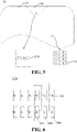
- the first display area 240 may have a plurality of first pixel groups 244. Each of the first pixel groups 244 may include a plurality of the first pixels 242 connected in parallel. One first pixel group 244 may include at least two first pixels 242, which may include at least two first pixels 242 of a same color, for example, red pixels. One first pixel group 244 may also include at least two first pixels 242 of different colors, for example, red pixels and green pixels.
- the plurality of first pixels 242 in one first pixel group 244 may be connected together by a plurality of signal lines.
- the signal lines may be made of a light-transmitting material.
- FIG. 5 is another partial schematic diagram of the display device shown in FIG. 2 .
- FIG. 5 shows a plurality of second driving units 224 in the second display area 220 and a plurality of first driving units 246 in the first display area 240.
- Each of the second driving units 224 may be electrically connected to one second pixel 222.
- Each of the second driving units 224 may drive one second pixel 222.
- Each of the first pixel group 244 may be electrically connected to one first driving unit 246.
- Each of the first driving units 246 may drive one first pixel group 244. That is, each of the first driving units 246 may drive all the first pixels 242 in one first pixel group 244.
- the first driving units 246 may be disposed in the first display area 240, for example, in the first driving portion 234. Because fewer first driving units 246 are required to drive the first pixels 242 in the first display area 240, the light transmittance of the first display area 240 is improved. It should be noted that FIG. 5 only shows some of the second driving units 224 and some of the first driving units 246 in the display device 20. In FIG. 5 , a size of a region formed by the arranged first driving units 246 is substantially same as a size of a region formed by the arranged second driving units 224.
- each of the first pixel groups 244 may be used as one first display unit in the first display area 240, that is, a smallest unit for displaying images in the first display area 240.
- each of the first pixel groups 244 as one first display unit includes four first pixels 242 of a same color, or sixteen first pixels 242 of a same color.
- each of the first pixel groups 244 as one first display unit includes multiple first pixels 242 with different colors.
- the plurality of second pixels 222 in the second display area 220 may form one second display unit, or a second pixel unit.
- the second pixel unit in the second display area 220 includes one red pixel, one green pixel, and one blue pixel.
- the second pixel unit in the second display area 220 may further include other pixels, such as one white pixel or one yellow pixel.
- multiple first pixel groups 244 may be used as one first display unit.
- three first pixel groups 244 may be used as one first display unit.
- four first pixel groups 244 may be used as one transparent display unit.
- Each of the first pixel groups 244 in one first display unit may include four first pixels 242 of the same color or sixteen first pixels 242 of the same color.
- one first display unit includes three first pixel groups 244.
- one first pixel group 244 includes four red pixels
- another first pixel group 244 includes four green pixels
- the third first pixel group 244 includes four blue pixels.
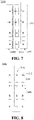
- FIG. 6 is a schematic diagram of a first arrangement of one first display unit in a first display area of the display device shown in FIG. 2 .
- One first display unit 216a in the first display area 240 may include three first pixel groups 244, which may be a first pixel group 244a, a first pixel group 244b, and a first pixel group 244c.
- the first pixel group 244a may include four red pixels 242 (R).
- the first pixel group 244b may include four green pixels 242 (G).
- the first pixel group 244c may include four blue pixels 242 (B). It should be noted that an arrangement of multiple first pixel groups in one first display unit is not limited to this arrangement.
- FIG. 7 is a schematic diagram of a second arrangement of one first display unit in the first display area of the display device shown in FIG. 2 .
- One first display unit 216b in the first display area 240 may include three first pixel groups 244, which may be a first pixel group 244d, a first pixel group 244e, and a first pixel group 244f.
- the first pixel group 244d may include four red pixels 242.
- the first pixel group 244e may include four green pixels 242.
- the first pixel group 244f may include four blue pixels 242.
- FIG. 8 is a schematic diagram of a third arrangement of one first display unit in the first display area of the display device shown in FIG. 2 .
- One first display unit 216c in the first display area 240 may include three first pixel groups 244, which may be a first pixel group 244h, a first pixel group 244i, and a first pixel group 244j.
- the first pixel group 244h may include four red pixels 242.
- the first pixel group 244i may include four green pixels 242.
- the first pixel group 244j may include four blue pixels 242.
- FIG. 9 is a schematic diagram of a fourth arrangement of one first display unit in the first display area of the display device shown in FIG. 2 .
- One first display unit 216d in the first display area 240 may include three first pixel groups 244, which may be a first pixel group 244k, a first pixel group 244m, and a first pixel group 244n.
- the first pixel group 244k may include four red pixels 242.
- the first pixel group 244m may include four green pixels 242.
- the first pixel group 244n may include four blue pixels 242.
- one first display unit in the first display area 240 includes four first pixel groups 244, the first pixels 242 included in each of the four first pixel groups 244 have a same color.
- one first pixel group 244 includes a plurality of red pixels
- a second first pixel group 244 includes a plurality of green pixels
- a third first pixel group 244 includes a plurality of blue pixels
- a fourth first pixel group 244 includes a plurality of white pixels.
- the fourth first pixel group 244 includes a plurality of yellow pixels.
- FIG. 6 to FIG. 9 only show some arrangements of one first display unit in the first display area 240 of the display device 20.
- one first display unit in the first display area 240 may have other arrangements.
- the size of the first pixels in the first display area may be set to be greater than the size of the second pixels in the second display area, and the first pixels in the first display area may be arranged more sparsely than the second pixels in the second display area. Therefore, the first pixels in the first display area and the second pixels in the second display area have different pixel physical structures. In an actual process, because the first pixels in the first display area and the second pixels in the second display area have different pixel physical structures, the pixel structures need to be formed through a series of processes such as exposure, development, and cleaning using different masks.
- the first pixels in the first display area need to be formed by a first type of mask through a first set of processes.
- the second pixels in the second display area need to be formed by a second type of mask through a second set of processes. This not only requires additional masks and tools, but also increases processes, increases processing cost and complexity, and reduces a yield of the pixels formed.
- the first pixels in the first display area and the second pixels in the second display area may be formed with a same tool, such as a mask, in a same process, so that the physical structure of each of the first pixels in the first display area is same as the physical structure of each of the second pixels in the second display area.
- the first display area needs to be provided with too many wires and the first driving units. Too many wires will affect the light transmittance of the first display area.
- At least two pixels in the first display area are connected in parallel to form one first pixel group. Multiple first pixels may be connected to one same signal line after being connected in parallel. Compared with each first pixel being connected to one signal line, the number of the signal lines may be greatly reduced, the arrangement of the signal lines may be facilitated, and the light transmittance of the first display area may be improved.
- At least two first pixels in the first display area are connected in parallel to form one first pixel group, which changes a wiring in a part of the display layer in the first display area without changing a pixel physical structure of the entire display device, so as to greatly reduce the number of the signal lines arranged in the first display area, thereby improving the light transmittance of the first display area.
- some of all the first driving units for driving the first display area 240 may be disposed in the first display area 240, and others may be disposed in other positions, such as in the second display area 220.
- some of the first driving units are disposed in the first driving portion 234, and the others are disposed in the second driving portion 232.
- all the first driving units for driving the first display area 240 may be disposed in other positions.
- all the first driving units may be disposed in the second display area 220.
- first driving units 246 for driving the first pixels 242 in the first display area 240 are disposed in the second display area 220, such as in the second driving portion 232, wires need to be arranged. Considering that the wires will occupy a space where the first display area 240 and the second display area 220 are connected, if there are too many wires, the space may not be enough to arrange the wires, and it is necessary to increase a thickness to arrange more wires.
- At least two first pixels 242 in the first display area 240 may be connected in parallel to form one first pixel group 244 and then connected to one same signal line, which can greatly reduce the number of the signal lines and the space occupied by the signal lines. Therefore, the first driving units 246 for driving the first pixels 242 in the first display area 240 may be disposed in the second display area 220.
- the second display area 220 is the main display area of the display device 20
- all the first driving units 246 for driving the first display area 240 are disposed in the second display area 220
- setting of the second driving portion 232 in the second display area 240 will be affected, and a wiring process of the second driving portion 232 may be affected. This may affect a quality and effect of images displayed in the second display area 220.
- a third display area may be disposed between the second display area 220 and the first display area 240 to form a transition.
- the first driving units may be disposed in the third display area to reduce the influence of the first driving units 246 on the second display area 220.
- FIG. 10 is another schematic structural diagram of the display device according to an embodiment of the present disclosure.
- the display device 20 may further include a third display area 260, which may also be referred to as a transition area.
- the third display area 260 may connect the second display area 220 and the first display area 240.
- the third display area 260 may be connected between the second display area 220 and the first display area 240.
- the third display area 260 may separate the second display area 220 from the first display area 240, so that the second display area 220 and the first display area 240 are not directly connected.
- the third display area 260 may connect a part of the second display area 220 and a part of the first display area 240, and other parts of the second display area 220 may be connected to other parts of the first display area 240.
- a size of the third display area 260 may be much less than a size of the second display area 220.
- the first display area 240 and the third display area 260 may together form an auxiliary display area of the display device 20.
- the first display area 240 and the third display area 260 may be defined as auxiliary display areas, or secondary display areas.
- FIG. 11 is a cross-sectional view of the display device shown in FIG. 10 along a line P4-P4.
- the display layer 210 may further include a third display portion 216 in the third display area 260.
- the third display portion 216 may be provided with a plurality of third pixels.
- An arrangement of the third pixels may be a standard RGB arrangement, a Pentile arrangement, or a Delta arrangement.
- the third pixels may be arranged in other ways.
- the driving layer 230 may further include a third driving portion 236.
- the third driving portion 236 may be provided with a plurality of driving units.
- the third driving portion 236 is provided with a plurality of third driving units, each of the third driving units may be electrically connected to one third pixel, and each of the third driving units may drive one third pixel.
- the third driving units may adopt 2T1C, 5T1C, or 7T1C.
- the third drive units adopt 5T1C.
- the third display area 260 may adopt 5T1C
- the first display area 240 may adopt 2T1C
- the second display area 220 may adopt 7T1C, so that the quality of the images displayed in the second display area 220 is greater than a quality of images displayed in the third display area 260, and the quality of the images displayed in the third display area 260 is greater than a quality of images displayed in the first display area 240. Therefore, a transition is presented between the first display area 240 and the second display area 220.
- Driving manners of the first display area 240, the second display area 220, and the third display area 260 are not limited to the above driving manners.
- the first display area 240 and the third display area 260 both adopt 5T1C
- the second display area 220 adopts 7T1C.
- FIG. 12 is a first partial schematic diagram of the display device shown in FIG. 10 .
- An arrangement of the third pixels 262 in the third display area 260 may be same as the arrangement of the second pixels 224 in the second display area 220, and may also be same as the arrangement of the first pixels 242 in the first display area 240.
- the second display area 220, the third display area 260, and the first display area 240 have a same pixel physical structure.
- the pixels in the second display area 220, the third display area 260, and the first display area 240 may be formed in a same process.
- the arrangement of the third pixels 262 in the third display area 260 may be different from the arrangement of the second pixels 224 in the second display area 220 or the arrangement of the first pixels 242 in the first display area 240. It should be noted that FIG. 11 only shows some pixels of the display device 20. In FIG. 11 , a size of a region formed by the arranged first pixels 242, a size of a region formed by the arranged third pixels 262, and a size of a region formed by the arranged second pixels 222 are substantially same.
- all the first driving units for driving the first display area 240 may be disposed in the third display area 260.
- the first driving units are disposed in the third display portion 236, so that a part of the driving layer in the first display area 240 has no first driving units.
- the first driving portion 234 in the first display area 240 has no thin film transistors. This can greatly improve the light transmittance of the first display area 240. Furthermore, this can avoid other problems caused by disposing the first driving units in the first display area 240, such as diffraction caused by the periodically arranged first driving units to imaging of the camera 60, and stray light caused by reflection and refraction of the first driving units to the imaging of the camera 60.
- the third display area 260 is provided with a plurality of third driving units
- the plurality of third driving units occupy a space of the third driving portion 236.
- the first driving units disposed in the third driving portion 236 also occupy the space of the third driving portion 236, and wires also occupy the space of the third driving portion 236.
- the wires in the third driving portion 236 may be set thinner, thereby reducing a space occupied by each signal line and accommodating more signal lines.
- the number of third driving units in the third display area 260 may be reduced, so that the first driving units can be disposed in the third driving portion 236 without changing a thickness of the wires in the third driving portion 236, and the wiring requirements can be met.
- the third display area 260 may be provided with a plurality of third pixel groups 264.
- Each of the third pixel groups 264 may include at least two third pixels 262 connected in parallel, and may include at least two third pixels 262 of a same color, such as red pixels.
- Each of the third pixel groups 264 may include at least two third pixels 262 of different colors, such as red pixels and green pixels.
- the third pixels 262 in one third pixel group 264 may be connected together by a plurality of signal lines.
- the number of the third pixels 262 in one third pixel group 264 may be more than the number of the first pixels 242 in one first pixel group 244.
- one third pixel group 264 includes four third pixels 262, and one first pixel group 244 includes sixteen first pixels 242.
- the number of the third pixels 262 in one third pixel group 264 may be same as the number of the first pixels 242 in one first pixel group 244.
- one of the third pixel groups 264 may be used as a third display unit in the third display area 260.
- a third pixel group 264 as one third display unit includes two third pixels 262 of the same color, or four third pixels 262 of the same color.
- a third pixel group 264 as one third display unit includes multiple third pixels 262 with different colors.
- multiple third pixel groups 264 may be used as one third display unit.
- three third pixel groups 264 may be used as one third display unit.
- four third pixel groups 264 may be used as one third display unit.
- Each of the third pixel groups 264 in one third display unit may include two third pixels 262 of the same color or four third pixels 262 of the same color.
- one third display unit includes three third pixel groups 264.
- one third pixel group 264 includes four red pixels
- another third pixel group 264 includes four green pixels
- the third third pixel group 264 includes four blue pixels.
- one first display unit in the third display area 260 includes four third pixel groups 264
- the third pixels 262 in each of the four third pixel groups 264 have a same color.
- one third pixel group 264 includes a plurality of red pixels
- a second third pixel group 264 includes a plurality of green pixels
- a third third pixel group 264 includes a plurality of blue pixels
- a fourth third pixel group 264 includes a plurality of white pixels.
- the fourth third pixel group 264 includes a plurality of yellow pixels.
- FIG. 13 is a second partial schematic diagram of the display device shown in FIG. 10 .
- FIG. 13 shows a plurality of second driving units 224 in the second display area 220, and a plurality of third driving units 266 and a plurality of first pixel units 246 in the third display area 260.
- the plurality of third driving units 266 and the plurality of second display units 246 are disposed in the third display area 260, for example, in the third driving portion 236.
- the plurality of third driving units 266 are configured to drive the third display area 260.
- Each of the third driving units 266 may be electrically connected to one third pixel group 264.
- Each of the third driving units 266 may drive one third pixel group 264. That is, each of the third driving units 266 may drive all the third pixels 262 in one third pixel group 264.
- this embodiment can reduce the number of the third driving units, thereby reducing a space of the third driving portion 236 occupied by the third driving units, so as to dispose the first driving units 246.
- each of the third driving units 266 includes four third pixels 262 connected in parallel.
- One third driving unit 266 may occupy a space corresponding to one third pixel 262, or a space slightly smaller than the space corresponding to the third pixel 262. Therefore, one third pixel group 264 may reserve spaces corresponding to at least three third pixels 262. Multiple first pixel units 264, such as three first driving units 246, may be disposed in the reserved spaces. The three spare third pixels 262 may be in a one-to-one correspondence with the three first driving units 246.
- At least two third pixels 262 in the third display area 260 may be connected in parallel to form one third pixel group 264, multiple third pixels 262 may be driven by one third driving unit 266, so that sufficient space is reserved in the third driving portion 236 for disposing the first driving units 246. Therefore, opaque thin film transistors in the first display area 240 may be disposed in the third display area 260 that does not need to collect light signals through cameras and the like.
- the size of the third display area 260 may be set smaller, and the third display area 260 connects the first display area 240 and the second display area 220. Therefore, in a case that images displayed in the second display area 220 are not greatly affected, deterioration of a quality of images displayed in the third display area 260 will not have a significant impact on a display effect of the entire display device 20.
- the number of the third pixels 262 connected in parallel in the third display area 260 may be less than the number of the first pixels 242 connected in parallel in the first display area 240, so that a display transition between the first display area 240 and the second display area 220 is smoother.
- the first driving units are not limited to be disposed in the third display area 260.
- some of the first driving units are disposed in the third display area 260, and the other first driving units are disposed in the first display area 240.
- some of the first driving units are disposed in the third display area 260, and the other first driving units are disposed in the second display area 220.
- the first driving units are divided into three parts, which are disposed in the first display area 240, the third display area 260, and the second display area 220, respectively.
- the first driving units are not limited to be disposed in a display area.
- the first driving units may be disposed in a side or a non-display area of the display device 20.
- FIG. 14 is a third partial schematic diagram of the display device shown in FIG. 10 .
- the display device 20 may further include a non-display area 280.
- the first driving units 246 for driving the first display area 240 may be disposed in the non-display area 280.
- the display device 20 may have a full screen. That is, a front surface of the display device 20 is substantially a display area. Viewed from a front surface of the electronic equipment, the front surface of the display device 20 is substantially equal to a display surface of the electronic equipment. However, even if the display device 20 has a full screen, the non-display area 280 still exists at an edge of the display device 20.
- the non-display area 280 may be understood as a black border of the display device 20.
- a width of the black border may be very narrow, for example, the width of the black border is less than 1 mm, 0.5 mm, or the like. Because the area of the first display area 240 is small, the number of the first pixels in the first display area 240 is relatively small. Furthermore, multiple first pixels in the first display area 240 may be connected in parallel. Therefore, the number of the first driving units 246 for driving the first display area 240 is reduced. Accordingly, the first driving units 246 may be disposed in the black border, which can improve the light transmittance of the first display area 240 without affecting the second display area 220 or the third display area 260. Multiple first driving units 246 need to be disposed corresponding to the first pixels in the first display area 240, and all the first driving units 246 may be disposed in the black border.
- first driving units 246 may adopt 2T1C, 5T1C, or other driving circuit, so that the number of thin film transistors in each of the first driving units 246 is small, and one first driving unit 246 requires less space.
- An arrangement density of the first pixels in the first display area 240 may be set smaller, so that a total number of the first driving units 246 configured to drive the first display area 240 is smaller.
- some of the first driving units 246 may be disposed in the non-display area 280 and the other first driving units 246 may be disposed in other position, such as in the first display area 240 or the third display area 260.
- the way of improving the light transmittance of the first display area 240 is not limited to the above way, and other ways may be used.
- wires in the first display area 240 of the display device 20 may be set to be transparent, so as to increase the light transmittance of the first display area 24.
- the first display area 240 may not be provided with a polarizing structure.
- the driving units for driving the first display area 240 may be driven in a passive way, which can greatly reduce the wires and components in the driving units. It can be understood that solutions of improving the first display area 240 by increasing a light transmittance of a material and changing an arrangement of wires fall within the claimed scope of the present application.
- the second display area 220 may be an active-driven (i.e. active-matrix organic light-emitting diode, AMOLED) display area
- the first display area 240 may be an active-driven display area or a passive-driven (i.e. passive-matrix organic light-emitting diode, PMOLED) display area.
- the area of the first display area 240 may be set to be less than the area of the second display area 220, so that a display content of the first display area 240 is less than a display content of the second display area 220, and an importance of the display content of the first display area 240 is lower than an importance of the display content of the second display area 220.
- the first display area 240 adopts PMOLED.
- the passive-driven first display area 240 can be driven by only one thin film transistor, so that the number of opaque thin film transistors is small, which greatly improve the light transmittance of the first display area 240.
- the area of the first display area 240 may be much less than the area of the second display area 220. Even if a quality of images displayed in the first display area 240 is reduced, an entire display of the display device 20 would not be greatly affected.
- the first display area 240 may be active-driven, so that a display effect of the first display area 240 is close to a display effect of the second display area 220.
- the third display area 260 may be configured as an active-driven display area or a passive-driven display area as required. Because a physical structure of the third pixels 262 in the third display area 260 is same as the physical structure of the first pixel 242 in the first display area 240, the third display area 260 and the first display area 240 may be driven in a same manner. For example, the third display area 260 and the first display area 240 may be passive-driven display areas. If the area of the third display area 260 is larger, or in order to improve a display quality of the third display area 260, the third display area 260 and the second display area 220 may be driven in a same manner, for example, may both be active-driven display areas.
- a size and shape of the first pixels 242 in the first display area 240 may be set as required.
- the first pixel 242 may be shaped as a rectangle or a circle-like shape.
- Circle-like first pixel 242 may be shaped as a circle, an ellipse, a rounded rectangle, or the like.
- the circle-like first pixels 242 can address diffraction problem of the first display area 240 because their edges are arc-shaped.
- the functional component of the electronic equipment 10, such as the camera 60 or the sensor may be disposed inside the display device 20.
- a lens of the camera 60 faces the lower substrate 270 of the display device 20, and the camera 60 is disposed corresponding to the first display area 240.
- the camera 60 is located below the lower substrate 270 in the first display area 240.
- the camera 60 can acquire external light signals passing through the first display area 240 for imaging.
- the lens of the camera 60 and the lower substrate 270 may be spaced apart.
- the lens of the camera 60 may be a part of the lower substrate 270.
- a part of the lower substrate 270 corresponding to the first display area 240 is formed into an arc-shaped structure.
- the lens of the camera 60 may be disposed close to or adjacent to the lower substrate 270 of the display device 20.
- the lower substrate 270 of the display device 20 is mainly configured to carry other layers of the display device 20 and does not need to have any special function.
- FIG. 15 is a schematic structural diagram of a cooperation of the display device in the electronic equipment and a camera according to an embodiment of the present disclosure.
- a part of the lower substrate 270 corresponding to the camera 60 may be provided with a first mounting hole 272.
- the camera 60 may be disposed at least partially in the first mounting hole 272.
- the first mounting hole 272 may be a blind hole. That is, a thickness of the part of the lower substrate 270 corresponding to the camera 60 is less than a thickness of other parts.
- the lower substrate 270 is still a complete substrate, its function of carrying other layers of the display device 20 is not affected, and a part of its space is reserved to accommodate the camera 60.
- the first mounting hole 272 and the camera 60 may be installed according to a size of the first mounting hole 272 and a size of the camera 60. For example, if a space of the first mounting hole 272 is not enough to install an entirety of the camera 60, the lens of the camera 60 may be disposed in the first mounting hole 272. If the camera is small enough, the entirety of the camera 60 may be disposed in the first mounting hole 272.
- the camera may be replaced with another functional device of the electronic equipment 10, such as a sensor. That is, at least a part of the sensor of the electronic equipment 10 may be disposed in the first mounting hole 272.
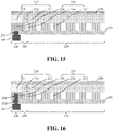
- FIG. 16 is another schematic structural diagram of the cooperation of the display device in the electronic equipment and the camera according to an embodiment of the present disclosure.
- the camera 60 may be installed in the driving layer.
- the first mounting hole 272 opened in the lower substrate 270 is a through hole.
- the part of the driving layer 230 in the first display area 240 is provided with a second mounting hole 238 corresponding to the camera 60.
- the first mounting hole 272 communicates with the second mounting hole 238.
- the camera 60 may be disposed at least partially in the second mounting hole 238.
- the lens of the camera 60 is disposed in the first mounting hole 272 and the second mounting hole 238.
- the second mounting hole 238 may be a through hole or a blind hole.
- the first mounting hole 272 and the second mounting hole 238 may be formed after some laminate layers of the display device 20 are formed. For example, after the driving layer 230 and the display layer 210 of the display device 20 are disposed on the lower substrate 270, the first mounting hole 272 and the second mounting hole 238 are formed in the parts of the driving layer 230 and the display layer 210 corresponding to the lens of the camera 60 using a laser or the like.
- the camera may be replaced with another functional device of the electronic equipment 10, such as a sensor. That is, at least a part of the sensor of the electronic equipment 10 may be disposed in the first mounting hole 272 and the second mounting hole 238.
- the camera 60 corresponding to the first display area 240 may be used as a front camera of the electronic equipment.
- a front camera is generally a camera with a lens that cannot be moved.
- the camera 60 corresponding to the first display area 240 may be a camera with a movable lens.
- the lens of the camera 60 can be moved to realize functions such as auto focus.
- the camera 60 may be a rear camera. That is, the electronic equipment 10 may be provided with two opposite display devices 20.
- One camera 60 or multiple cameras 60 may be disposed under the first display area 240.
- the multiple cameras 60 may be cameras 60 that cooperate with each other, such as two identical cameras, a normal camera, and a bokeh camera or a black-and-white camera.
- other functional devices such as a proximity sensor, a light sensor, a ranging sensor, a fingerprint recognition sensor, and the like, may be further disposed under the first display area 240.
- the electronic equipment 10 may further include a housing 40.
- the housing 40 may be made of plastic, glass, ceramic, a fiber composite, a metal (e.g. stainless steel and aluminum), other suitable material, or a combination of any two or more of these materials.
- the housing 40 may be integrally formed. In an integrally formed process, some or all of the housing 40 is machined or molded as a single structure, or may be formed from multiple structures (e.g. an inner frame structure, and one or more structures forming an outer housing surface).
- the housing 40 may be provided with a receiving cavity to receive components of the electronic equipment 10 such as a battery, a circuit board, and the like.
- the housing 40 may carry the display device 20.
Landscapes
- Engineering & Computer Science (AREA)
- Physics & Mathematics (AREA)
- Computer Hardware Design (AREA)
- General Physics & Mathematics (AREA)
- Theoretical Computer Science (AREA)
- Geometry (AREA)
- Microelectronics & Electronic Packaging (AREA)
- Devices For Indicating Variable Information By Combining Individual Elements (AREA)
Applications Claiming Priority (3)
| Application Number | Priority Date | Filing Date | Title |
|---|---|---|---|
| CN201921866088.XU CN210378421U (zh) | 2019-10-31 | 2019-10-31 | 显示装置和电子设备 |
| CN201911049708.5A CN110634445A (zh) | 2019-10-31 | 2019-10-31 | 显示装置和电子设备 |
| PCT/CN2020/118915 WO2021082856A1 (fr) | 2019-10-31 | 2020-09-29 | Appareil d'affichage et dispositif électronique |
Publications (2)
| Publication Number | Publication Date |
|---|---|
| EP4016513A1 true EP4016513A1 (fr) | 2022-06-22 |
| EP4016513A4 EP4016513A4 (fr) | 2022-09-28 |
Family
ID=75715781
Family Applications (1)
| Application Number | Title | Priority Date | Filing Date |
|---|---|---|---|
| EP20882197.5A Withdrawn EP4016513A4 (fr) | 2019-10-31 | 2020-09-29 | Appareil d'affichage et dispositif électronique |
Country Status (3)
| Country | Link |
|---|---|
| US (1) | US20220173170A1 (fr) |
| EP (1) | EP4016513A4 (fr) |
| WO (1) | WO2021082856A1 (fr) |
Families Citing this family (4)
| Publication number | Priority date | Publication date | Assignee | Title |
|---|---|---|---|---|
| CN112151592B (zh) * | 2020-09-30 | 2022-10-04 | 武汉天马微电子有限公司 | 显示面板及显示装置 |
| CN112909024B (zh) * | 2021-02-03 | 2022-08-02 | 武汉华星光电半导体显示技术有限公司 | 显示面板及其制备方法、显示装置 |
| US12426445B1 (en) * | 2021-04-01 | 2025-09-23 | Apple Inc. | Devices with displays having transparent openings and shorted pixels |
| CN115524880B (zh) * | 2021-06-24 | 2025-10-03 | 群创光电股份有限公司 | 显示装置 |
Family Cites Families (15)
| Publication number | Priority date | Publication date | Assignee | Title |
|---|---|---|---|---|
| WO2019062236A1 (fr) * | 2017-09-30 | 2019-04-04 | 昆山国显光电有限公司 | Écran d'affichage, procédé d'attaque d'écran d'affichage et dispositif d'affichage correspondant |
| CN207781599U (zh) * | 2017-09-30 | 2018-08-28 | 云谷(固安)科技有限公司 | 显示屏以及电子设备 |
| CN112908238B (zh) * | 2017-10-27 | 2023-06-23 | 武汉天马微电子有限公司 | 一种显示面板和电子设备 |
| CN109872670B (zh) * | 2017-12-05 | 2021-11-05 | 京东方科技集团股份有限公司 | 显示屏、显示装置、显示电路及其亮度补偿方法 |
| US10707281B2 (en) * | 2018-08-10 | 2020-07-07 | Au Optronics Corporation | Display apparatus |
| CN109584794A (zh) * | 2019-01-25 | 2019-04-05 | 京东方科技集团股份有限公司 | 一种显示面板及显示装置 |
| KR102770831B1 (ko) * | 2019-02-07 | 2025-02-24 | 삼성디스플레이 주식회사 | 표시 장치 |
| US11031443B2 (en) * | 2019-04-15 | 2021-06-08 | Wuhan China Star Optoelectronics Semiconductor Display Technology Co., Ltd. | Organic light-emitting diode (OLED) display device including sensor disposed in groove of base substrate |
| CN110047386B (zh) * | 2019-04-30 | 2021-12-31 | 武汉天马微电子有限公司 | 一种显示装置和电子设备 |
| CN210245501U (zh) * | 2019-07-03 | 2020-04-03 | 昆山国显光电有限公司 | 阵列基板、显示面板及显示装置 |
| CN110265472A (zh) * | 2019-07-15 | 2019-09-20 | 京东方科技集团股份有限公司 | 一种显示面板及显示装置 |
| CN110392146B (zh) * | 2019-07-17 | 2025-01-07 | 北京小米移动软件有限公司 | 终端屏幕及终端 |
| CN110634445A (zh) * | 2019-10-31 | 2019-12-31 | Oppo广东移动通信有限公司 | 显示装置和电子设备 |
| CN110706649B (zh) * | 2019-10-31 | 2022-02-22 | Oppo广东移动通信有限公司 | 显示装置及电子设备 |
| CN110599944B (zh) * | 2019-10-31 | 2024-10-11 | Oppo广东移动通信有限公司 | 显示装置及电子设备 |
-
2020
- 2020-09-29 WO PCT/CN2020/118915 patent/WO2021082856A1/fr not_active Ceased
- 2020-09-29 EP EP20882197.5A patent/EP4016513A4/fr not_active Withdrawn
-
2022
- 2022-02-21 US US17/676,464 patent/US20220173170A1/en not_active Abandoned
Also Published As
| Publication number | Publication date |
|---|---|
| WO2021082856A1 (fr) | 2021-05-06 |
| EP4016513A4 (fr) | 2022-09-28 |
| US20220173170A1 (en) | 2022-06-02 |
Similar Documents
| Publication | Publication Date | Title |
|---|---|---|
| CN210516183U (zh) | 显示装置和电子设备 | |
| US20220173170A1 (en) | Display device and electronic equipment | |
| CN110783487B (zh) | 显示装置及电子设备 | |
| CN110599944B (zh) | 显示装置及电子设备 | |
| US20220190082A1 (en) | Display apparatus and electronic device | |
| US20220190084A1 (en) | Display apparatus and electronic device | |
| CN110675825B (zh) | 显示装置和电子设备 | |
| CN110767729B (zh) | 显示装置及电子设备 | |
| US12396325B2 (en) | Display device and electronic device having display layer, second driving layer, and first driving layer stacked in sequence | |
| US11990086B2 (en) | Display apparatus and electronic device | |
| CN114144827B (zh) | 显示装置及电子设备 | |
| CN110634445A (zh) | 显示装置和电子设备 | |
| CN110648622A (zh) | 显示装置及电子设备 | |
| US12342690B2 (en) | Display apparatus with light-shielding portion adjoining substrate and anode, manufacturing method for display apparatus, and electronic device | |
| WO2021082983A1 (fr) | Appareil d'affichage et dispositif électronique | |
| CN210378415U (zh) | 显示装置及电子设备 | |
| CN210516182U (zh) | 显示装置及电子设备 | |
| CN110728921A (zh) | 显示装置及电子设备 | |
| CN210378421U (zh) | 显示装置和电子设备 | |
| CN110767727B (zh) | 电子设备 | |
| CN112366216B (zh) | 显示装置和电子设备 | |
| CN110740244A (zh) | 电子设备及其控制方法和拍照方法 |
Legal Events
| Date | Code | Title | Description |
|---|---|---|---|
| STAA | Information on the status of an ep patent application or granted ep patent |
Free format text: STATUS: THE INTERNATIONAL PUBLICATION HAS BEEN MADE |
|
| PUAI | Public reference made under article 153(3) epc to a published international application that has entered the european phase |
Free format text: ORIGINAL CODE: 0009012 |
|
| STAA | Information on the status of an ep patent application or granted ep patent |
Free format text: STATUS: REQUEST FOR EXAMINATION WAS MADE |
|
| 17P | Request for examination filed |
Effective date: 20220316 |
|
| AK | Designated contracting states |
Kind code of ref document: A1 Designated state(s): AL AT BE BG CH CY CZ DE DK EE ES FI FR GB GR HR HU IE IS IT LI LT LU LV MC MK MT NL NO PL PT RO RS SE SI SK SM TR |
|
| A4 | Supplementary search report drawn up and despatched |
Effective date: 20220831 |
|
| RIC1 | Information provided on ipc code assigned before grant |
Ipc: H01L 27/32 20060101ALI20220825BHEP Ipc: G09G 3/3225 20160101ALI20220825BHEP Ipc: G09G 3/3216 20160101AFI20220825BHEP |
|
| DAV | Request for validation of the european patent (deleted) | ||
| DAX | Request for extension of the european patent (deleted) | ||
| STAA | Information on the status of an ep patent application or granted ep patent |
Free format text: STATUS: EXAMINATION IS IN PROGRESS |
|
| 17Q | First examination report despatched |
Effective date: 20240516 |
|
| STAA | Information on the status of an ep patent application or granted ep patent |
Free format text: STATUS: THE APPLICATION IS DEEMED TO BE WITHDRAWN |
|
| 18D | Application deemed to be withdrawn |
Effective date: 20240917 |