EP4016576B1 - Dispositif de commutation électrique pour applications moyenne et/ou haute tension - Google Patents
Dispositif de commutation électrique pour applications moyenne et/ou haute tension Download PDFInfo
- Publication number
- EP4016576B1 EP4016576B1 EP20214203.0A EP20214203A EP4016576B1 EP 4016576 B1 EP4016576 B1 EP 4016576B1 EP 20214203 A EP20214203 A EP 20214203A EP 4016576 B1 EP4016576 B1 EP 4016576B1
- Authority
- EP
- European Patent Office
- Prior art keywords
- switching device
- coating
- housing
- refraction
- controlling coating
- Prior art date
- Legal status (The legal status is an assumption and is not a legal conclusion. Google has not performed a legal analysis and makes no representation as to the accuracy of the status listed.)
- Active
Links
Images

Classifications
-
- H—ELECTRICITY
- H01—ELECTRIC ELEMENTS
- H01H—ELECTRIC SWITCHES; RELAYS; SELECTORS; EMERGENCY PROTECTIVE DEVICES
- H01H33/00—High-tension or heavy-current switches with arc-extinguishing or arc-preventing means
- H01H33/60—Switches wherein the means for extinguishing or preventing the arc do not include separate means for obtaining or increasing flow of arc-extinguishing fluid
- H01H33/66—Vacuum switches
- H01H33/662—Housings or protective screens
-
- H—ELECTRICITY
- H01—ELECTRIC ELEMENTS
- H01H—ELECTRIC SWITCHES; RELAYS; SELECTORS; EMERGENCY PROTECTIVE DEVICES
- H01H33/00—High-tension or heavy-current switches with arc-extinguishing or arc-preventing means
- H01H33/60—Switches wherein the means for extinguishing or preventing the arc do not include separate means for obtaining or increasing flow of arc-extinguishing fluid
- H01H33/66—Vacuum switches
- H01H33/662—Housings or protective screens
- H01H33/66207—Specific housing details, e.g. sealing, soldering or brazing
-
- H—ELECTRICITY
- H01—ELECTRIC ELEMENTS
- H01H—ELECTRIC SWITCHES; RELAYS; SELECTORS; EMERGENCY PROTECTIVE DEVICES
- H01H33/00—High-tension or heavy-current switches with arc-extinguishing or arc-preventing means
- H01H33/60—Switches wherein the means for extinguishing or preventing the arc do not include separate means for obtaining or increasing flow of arc-extinguishing fluid
- H01H33/66—Vacuum switches
- H01H33/662—Housings or protective screens
- H01H33/66207—Specific housing details, e.g. sealing, soldering or brazing
- H01H2033/6623—Details relating to the encasing or the outside layers of the vacuum switch housings
Definitions
- the invention relates to an electrical switching device, in particular for medium and/or high voltage applications, comprising at least two contactable conductor elements which can be separated by a movement device and a housing defining a switching chamber made of one or more insulators, wherein parts of the switching chamber can be made of metal, usually in the vicinity of the contact gap, and two caps, preferably made of metal, which axially close off the housing,
- VEB vacuum circuit breakers
- These are core components in energy transmission and distribution, particularly in their switching systems. They cover a large part of medium-voltage switching applications, i.e. switching applications in the range from 1 kV to 52 kV, for example, as well as a relevant part in low-voltage systems. Their use in high-voltage transmission systems, for example at voltages greater than 52 kV, is also increasing.
- a VCB While a VCB is closed most of the time, thus providing contact between the conductor elements, its main task is to interrupt currents in alternating current systems under nominal conditions, in particular for switching nominal currents on and off, or preferably for interrupting currents under fault conditions, in particular to prevent short circuits. to interrupt and protect the system.
- Other applications include pure switching of load currents using contacting conductor elements, which is mostly used in low and medium voltage systems.
- the vacuum interrupter (VI, also vacuum switching tube) is the core element of a VCB.
- a vacuum switching tube usually has a pair of contacts that are formed by corresponding conductor elements, at least one of which can be moved by means of a movement device in order to be able to bring about the open and closed states of the switching device.
- one conductor element is moved axially with respect to the other fixed conductor element.
- the contacts can be made of current-conducting bolts, in particular made of metal, which provide both current and heat conduction as well as the mechanical means to hold and/or move the contacts.
- a VI further comprises a vacuum-tight housing and the mentioned movement device and can also comprise a metal bellows which is connected on one side to the housing and on the other side to the moving conductor element, in particular the moving bolt.
- the housing is essentially formed by an insulating component, i.e. an insulator, for example a ceramic tube, which is connected to the conductor elements via connecting elements, whereby metal caps or the like are used, for example, which close off the insulating component in the axial direction to form the switching chamber.
- the switching device When the switching device is in an open state, it is necessary to isolate the nominal voltage of the system, but also to isolate high amplitude surge voltages, for example can be triggered by a lightning strike into the system.
- the switching device changes from the closed to the open state, thus separating the contacts of the conductor elements, rated currents or short-circuit currents must be interrupted, which lead to the appearance of temporary voltage peaks across the VI that are significantly higher than the rated AC voltages of the system.
- High voltages in vacuum systems typically generate free electrons through field emission processes if the electric field strength is sufficiently high.
- the acceleration of the electrons in the high electric fields increases the kinetic energy of these electrons, for example up to energies exceeding several tens or even hundreds of KeV.
- the interaction of these high-energy electrons with the housing structures leads to the production of high-energy X-rays that can leave the vacuum interrupter.
- the fault current within the vacuum interrupter is minimal and does not generate any significant X-rays, circumstances may arise, for example when transient high-amplitude voltage spikes occur, in which the resulting X-rays generate free electrons on and/or near the outer surface of the insulator.
- These electrons can be accelerated by the electric fields on and near the insulator surface, disrupt the electric field distribution in sensitive areas and lead to gas breakdown, resulting in a failure in the operation of the vacuum interrupter.
- a shielding element which can also be made of metal, in the contact area of the conductor elements to catch free metal particles from the conductor elements, but this also has an influence on the field distribution within the switching chamber, but also on the insulator.
- the housing of the switching chamber and in particular the insulator, which is usually made of ceramic, must be able to withstand high voltages across its surface, even in the presence of X-rays and free electrons or, in some cases, even when the insulator is contaminated by dust particles that are electrostatically deposited on the outer surface of the insulator. Since the insulator contributes significantly to the cost of a vacuum interrupter (or other switching device) and also negatively influences the cost of other structural elements of the vacuum interrupter (or other switching device), it is necessary to optimize the housing in order to achieve maximum dielectric strength with minimum component size.
- the known VIs are often constructed largely symmetrically to an -imaginary- center plane of the tube in order to minimize the number of different components and the complexity of the structure.
- the real environment of the tube generally distorts the electric field strongly, so that areas of the tube are strongly electric - in the sense of a high average electric field strength.
- This object is achieved by the subject matter of the present invention, as disclosed in the description, the figures and the claims.
- Permittivity is the ability of a material to be polarized by electric fields. Permittivity is a material property of electrically insulating polar or non-polar compounds that only becomes apparent when these compounds are exposed to an electric field.
- the matrix material can be selected from the group comprising elastomers, thermosets, thermoplastics and/or glass.
- the various coating processes for producing the coating can be selected accordingly.
- the matrix material is preferably applied as a paint, particularly in the form of a wet paint or powder paint.
- Other application methods such as spraying, immersion baths, casting, etc. are conceivable, but they are not the main focus of current research into the technology.
- the great advantage of applying the coating as a powder coating and/or wet coating is that the refractively controlling coating produced is free of pores. Such a pore-free coating can also be achieved by casting, but the homogeneity of the coating usually suffers, especially at the edges.
- this When applied as a wet paint, this usually contains solvents which are not present in the matrix material or are only present in small quantities after the paint has dried.
- the matrix is made of a polymeric matrix material, for example a polymeric resin, which is in the form of a polymeric binder.
- a "polymer matrix” refers to a polymer or a polymeric binder.
- the polymeric matrix comprises in particular a resin or a resin mixture, such as epoxy resin, silicone elastomer, siloxane resin, silicone resin, polyvinyl alcohol, polyester imide and similar thermosetting, thermoplastic plastics, as well as any combinations, copolymers, blends and mixtures of the above-mentioned resins and/or plastics.
- the matrix preferably contains fillers with a high permittivity to air, in particular refractive dielectric insulating fillers, such as ceramic fillers, which are polar and/or easily polarizable in an electric field.
- the materials for the filler(s) are selected from Class 1 ceramic materials that meet high stability requirements and whose permittivities have a low dependence on temperature and field strength.
- These include, for example, compounds such as selected titanates, which have reproducibly low temperature coefficients and low dielectric losses. Their permittivity is largely independent of field strength, which has advantages for the application in question here.
- Fillers made of a material that is commercially available in the field of capacitor ceramics and is therefore relatively cheap and available in sufficient quantities are preferred.
- materials that have an almost linear temperature profile of the capacitor capacitance are considered.
- these are in the form of one or more ceramics, in particular ceramics with metal nitride, metal carbide, metal boride and/or metal oxides such as titanium dioxide, aluminum oxide, selected compounds of ceramics comprising titanate are also suitable because of their field strength-independent permittivity.
- oxides of metal alloys in any combination with all of the aforementioned materials are also particularly suitable for fillers that exhibit largely field strength-independent permittivity.
- a mixture of finely ground paraelectrics such as titanium dioxide with admixtures of magnesium (Mg), zinc (Zn), zirconium (Zr), niobium (Nb), tantalum (Ta), cobalt (Co) and/or strontium (Sr) is suitable as a material for such a filler.
- thermosets and thermoplastics can be applied in the form of a powder coating.
- a hardener is present when additive polymerization takes place.
- An accelerator, initiator and/or catalyst is used in all cases where resin is cured.
- the matrix material is usually applied before, during, but preferably after the manufacture of the housing.
- the refractive-controlling layer which is produced by coating with the matrix material, is applied by spraying, doctoring, dipping, brushing and/or other methods that enable the production of a thin, homogeneous - in particular allowing for a coating that is as homogeneous and pore-free as possible.
- the application method is preferably carried out automatically.
- the refractively controlling coating is preferably a filled coating made of one or more matrix materials, which can be organic, for example in the form of a polymer, or inorganic, for example as glass, in which the filler is introduced.
- the amount of filler in the refractively controlling coating can vary within wide limits.
- a filler concentration of 1 vol.% - i.e. the almost unfilled matrix material with a relatively low refraction, which is caused almost exclusively by the dielectric barrier formed by the matrix material - can be present in the coating up to a filling of 70 vol.%.
- the preferred range of filler quantity is between 20 and 60 vol.%, in particular from 30 vol.% to 40 vol.% filling in the matrix material.
- the filler particles of the refractive-controlling coating do not have a preferred shape; they can be embedded in the matrix in any shape and size.
- the filler particles are irregular after appropriate grinding.
- Filled paints whose particles are as close as possible to a spherical shape, are more suitable for processing than other shapes because the specific surface area is the smallest and thus the smallest possible processing viscosity is achieved with the same degree of filling.
- the size of the fillers can vary. There can be different filler fractions in the filler.
- the housing can be provided with differently filled coatings in different areas.
- Thicker coatings and/or certain material combinations result in a stronger refraction of the field lines than others.
- the level of permittivity and the thickness of the applied refractive-controlling coating determine how much the electric field is evened out.
- thicknesses of the refractive-controlling coating of 10 ⁇ m to 5 mm, preferably in the range between 100 pm and 3 mm, particularly preferably in the range between 500 pm and 2 mm, have proven to be expedient.
- the permittivity of the coating according to an embodiment of the invention - filled or unfilled - is used so that the electric field on the surface of the housing of the switching chamber is pushed away by the increased permittivity compared to the uncoated surface and local field increases are thus reduced. This is explained again and shown schematically in Figure 2.
- the surface of the housing would usually be covered by an insulating gas such as nitrogen, air or sulphur hexafluoride. All of these gases have a comparatively low permittivity.
- the refractively controlled coating proposed here breaks the emerging field lines according to the refractive field control - refraction - because the penetration of the field into the higher permittivity material is made more difficult by the displacement of the field from the material with a higher permittivity into the material with a lower permittivity material. because the electric field is pushed away from the edge or triple point.
- the triple point is the area of the housing in which a metal electrode, a solid insulator and a gaseous insulator - in this case the surrounding gas - come together.
- the refractively controlling coating is at least partially applied to at least one of the contacting sides of the housing.
- the refractively controlling coating is also a dielectric barrier which, when applied to the metal electrodes, ensures that electrons have a much harder time getting out of the metal. Or, in other words, the electrical arcing between the electrodes is shifted towards higher voltages by the dielectric barrier. The refractive field shift then also shifts it towards even higher voltages.
- the refractive-controlling coating is provided on both metallic caps of the housing, which axially close off the preferably cylindrical insulator body to form the switching chamber, in whole or in part in addition to the application on the insulator body.
- the refractive-controlling coating covers the housing completely or partially or in selected areas.
- the refractive-controlling coating is applied directly to the housing surface or, for example, to a lower layer, such as a resistive layer after the EP 3146551 B1 .
- a lower layer on which the refractive-controlling coating is applied can comprise a further refractive-controlling layer as well as another, in particular a resistive layer after the EP 3146551 B1 , but preferably also, as an alternative, a resistive-capacitive layer.
- the lower layer is a thinner layer than the upper one, so that the layer thicknesses increase from the inside to the outside on the housing outer surface.
- the matrix materials of the respective coatings are compatible with one another. It is preferred, for example, that the matrix materials are at least inert to one another, but advantageously they can be mixed with one another and/or into one another as desired. It is very preferred that the matrix materials of different layers - for example the matrix material of a refractively controlling coating according to an embodiment of the present invention and the matrix material of a resistive coating according to the EP 3146551 B1 - have the same or similar chemical composition.
- the coatings can also be combined in the form of layer stacks, with a resistive coating according to the EP 3146551 B1 preferably on the insulating areas of the housing of the switching device, such as on a ceramic cylinder, whereas the refractively controlling coating is provided in particular on the caps of the housing, i.e. the contacting areas.
- both coatings can extend over one another as desired and in particular also over all areas of the housing on the outside.
- All layers of the overall coating of the housing cover the respective parts of the housing completely or partially, but on the outside.
- refractive-controlling coating is not applied over the entire surface of the housing, but only partially covers the housing. It is particularly preferred if the refractively controlling coating is applied to the caps, in particular to the metal caps and/or to the edges that form the caps with the insulator body.
- the refractively controlling coating extends beyond the edge, forming a border, for example also onto the surface of the insulator body.
- the insulator body itself is coated, for example with a resistive coating, or not.
- the resistive layer is applied over the entire surface of the housing outer surface, according to the present invention it can, in contrast, also only partially cover the outside of the housing, in particular it can also be applied in the form of a resistive-capacitive layer with a non-galvanically - i.e. not via a contact - electrically conductively connected area.
- the lower layer is thinner than the upper layer.
- the refractive-controlling layer is located on the resistive layer.
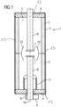
- FIG. 1 shows in the form of a schematic diagram an embodiment of a switching device 1 according to the invention, here a vacuum interrupter.
- a housing 3 which is composed of two tubular ceramic parts, i.e. insulator bodies 2, is closed off by metal caps 4, which form areas with electrical contacts, and defines a switching chamber 5, into which two conductor elements 6, designed for example as bolts, with contacts 7 are guided.
- the lower of the conductor elements 6 is designed to be movable according to the arrow 8 and the indicated movement device 9 and can be moved in the direction of extension 10 of the conductor elements 6, which also forms the axis of symmetry of the switching device 1, in order to bring the contacts 7 into contact or to space them apart, whereby in the present case an open, i.e. spaced-apart, state of the switching device 1 is shown.
- the invention also relates to gas switches in which the gas is present inside the switch.
- the gas switches included here are those in which gas serves as a switching medium and, after successful shutdown, as an insulating medium.
- SF6 is usually used for this nowadays. Since SF6 is to be replaced as a strong greenhouse gas, switches with CO2, fluoronitrile or other alternative gases are also conceivable in the future.
- a metal shielding element 12 (vapor shield) is provided in the contact area in the switching chamber 5.
- this shielding element 12 also causes a distortion of the electric field, so that in an area behind the shielding elements there would be a lower electric field during operation than in the "unshielded" areas, where charges can accumulate, for example, and thus cause further field distortions that could jeopardize the functionality of the switching device 1.
- a refractive-controlling coating 13 is located on the outer surface of the housing 3, i.e. both on the insulator body 3 and on areas of the electrical contacts - i.e. the caps 4.
- the refractively controlling coating 13 of the embodiment shown here which is applied over the entire surface, comprises a polymer matrix which is filled with a highly permittive filler made of a ceramic material ⁇ r in the range of greater than or equal to 2 to 200, preferably from 10 to 100.
- the filler is contained in the matrix at 30 vol%. It is a mixture of titanium dioxide and aluminum oxide particles.
- the refractive-controlling coating 13 is relatively inexpensive in terms of material price and relatively easy to spray on - even automatically. Its presence can be relatively easily detected using a scanning electron microscope and elemental analysis.
- the Figure 2 shows schematically the effect of a refractive-controlling coating on a housing outer surface such as the one in Figure 1 shown housing 3.
- Figure 2 shows schematically the course of the field and equipotential lines 15, 14 at each triple point, right half with a refractive-controlling coating 13 and left half for comparison without such a coating, according to the state of the art.
- the field lines 15 on the left run unbroken from the metal cap 4 into the surrounding gas, e.g. air. This can result in lightning discharges 16.
- the field lines 15 are broken at the transition from the coating with high permittivity to the surrounding air with low permittivity - see area 17 - this breaks both the equipotential lines 14 and the field lines 15 are pulled far apart so that no arcs occur.
- the refractively controlling coating 13, as proposed for the first time for this application, can reduce the length of the housing 3 of a switching device 1 and thus the overall length of the electrical switching device 1. This saves material costs.
- a housing 3 could be produced for a specific voltage level.
- This exact housing 3 could then be coated with the refractively controlling coating 13 according to an embodiment of the present invention, and thus be usable for the next higher voltage level. In terms of process technology, this results in a design that can be used for two voltage levels, with the same two housings 3 being usable for two switching devices 1 at different voltage levels!
- the two housings differ only in the additional refractive-controlling coating 13.
- the present invention is not limited to vacuum tubes, but relates to other switches, for example gas-insulated ones - for example those with SF6 and/or clean air - as switching gas.
- gas switches with clean air this is usually only used as an insulating medium and is not located in the interrupter unit, where the arc is created and the switching action is carried out.
Landscapes
- Organic Insulating Materials (AREA)
- Insulating Bodies (AREA)
- Insulators (AREA)
- Inorganic Insulating Materials (AREA)
- Gas-Insulated Switchgears (AREA)
Claims (16)
- Dispositif de commutation électrique (1) avec au moins deux éléments conducteurs (6) pouvant être mis en contact, pouvant être espacés par l'intermédiaire d'un dispositif de déplacement (9) et un boîtier (3) définissant une chambre de commutation (5), lequel entoure au moins en partie les éléments conducteurs (6), dans lequel le boîtier (3) a un corps isolant (2) et des zones d'un contact électrique (4) et dans lequel le boîtier (3) comprend à l'extérieur au moins en partie un revêtement à commande réfractive (13), lequel comporte une matrice diélectriquement isolante en un matériau d'une permittivité εr >/= 2, caractérisé en ce que la matrice du revêtement à commande réfractive contient une matière de charge, dans lequel le matériau des particules de matière de charge de l'au moins une fraction de matière de charge est une matière céramique avec une permittivité comprise dans la gamme de εr >/= 3 et εr </= 200.
- Dispositif de commutation selon la revendication 1, dans lequel le revêtement à commande réfractive se situe au moins dans une zone d'un contact électrique (4).
- Dispositif de commutation selon la revendication 1 ou la revendication 2, dans lequel le matériau des particules de matière de charge de l'au moins une fraction de matière de charge comporte une matière céramique avec au moins un oxyde métallique, un oxyde métallique mixte et/ou un titanate.
- Dispositif de commutation selon l'une des revendications précédentes, dans lequel, dans la matrice, une quantité totale de particules de matière de charge se situe dans la gamme allant de 1 % en volume à 70 % en volume.
- Dispositif de commutation selon l'une des revendications précédentes, dans lequel la résine est sélectionnée dans le groupe des élastomères, des duroplastiques, des thermoplastiques et/ou du verre.
- Dispositif de commutation selon l'une des revendications précédentes, dans lequel la matrice est une résine polymère et/ou un mélange de résines polymères.
- Dispositif de commutation selon l'une des revendications précédentes, dans lequel la résine polymère ou le mélange de résines polymères comporte au moins un composé sélectionné dans le groupe des composés suivants : une résine époxyde, un élastomère de silicone, une résine siloxane, une résine silicone, un alcool polyvinylique, un polyesterimide, ainsi que des mélanges et/ou combinaisons quelconques des composés précédents.
- Dispositif de commutation selon l'une des revendications précédentes, dans lequel le revêtement à commande réfractive est prévu en combinaison avec au moins un revêtement supplémentaire sur la surface extérieure du boîtier (13).
- Dispositif de commutation selon la revendication 8, dans lequel le revêtement supplémentaire est un revêtement résistif.
- Dispositif de commutation selon l'une des revendications précédentes, dans lequel le revêtement résistif recouvre en totalité ou en partie la surface extérieure du boîtier.
- Dispositif de commutation selon l'une des revendications précédentes, dans lequel le revêtement à commande réfractive (13) est prévu au moins en partie par-dessus le revêtement résistif.
- Dispositif de commutation selon l'une des revendications précédentes, dans lequel le revêtement à commande réfractive présente une épaisseur de couche inférieure ou égale à 5 mm.
- Dispositif de commutation selon l'une des revendications précédentes, dans lequel le revêtement à commande réfractive présente une épaisseur de couche inférieure ou égale à 2 mm.
- Dispositif de commutation selon l'une des revendications précédentes, dans lequel le revêtement à commande réfractive est applicable sous forme de peinture liquide.
- Dispositif de commutation selon l'une des revendications précédentes, dans lequel le revêtement à commande réfractive est applicable sous forme de peinture en poudre.
- Dispositif de commutation selon l'une des revendications précédentes, dans lequel, en ce qui concerne le dispositif de commutation, il s'agit d'un commutateur à vide ou d'un commutateur à gaz.
Priority Applications (9)
| Application Number | Priority Date | Filing Date | Title |
|---|---|---|---|
| EP20214203.0A EP4016576B1 (fr) | 2020-12-15 | 2020-12-15 | Dispositif de commutation électrique pour applications moyenne et/ou haute tension |
| ES20214203T ES2994802T3 (en) | 2020-12-15 | 2020-12-15 | Electrical switching device for medium and / or high voltage applications |
| HUE20214203A HUE069376T2 (hu) | 2020-12-15 | 2020-12-15 | Elektromos kapcsolószerkezet közép- és/vagy nagyfeszültségû alkalmazásokhoz |
| JP2023536128A JP2023554041A (ja) | 2020-12-15 | 2021-12-14 | 中電圧および/または高電圧用途のための電気開閉装置 |
| EP21839136.5A EP4244879A1 (fr) | 2020-12-15 | 2021-12-14 | Dispositif de commutation électrique pour utilisations à moyenne et/ou haute tension |
| KR1020237023780A KR20230118954A (ko) | 2020-12-15 | 2021-12-14 | 중전압 및/또는 고전압 용도들을 위한 전기 스위칭디바이스 |
| CN202180093829.9A CN116848608A (zh) | 2020-12-15 | 2021-12-14 | 用于中压和/或高压应用的电气开关设备 |
| PCT/EP2021/085728 WO2022129073A1 (fr) | 2020-12-15 | 2021-12-14 | Dispositif de commutation électrique pour utilisations à moyenne et/ou haute tension |
| US18/257,533 US12518937B2 (en) | 2020-12-15 | 2021-12-14 | Electric switching device for medium- and/or high-voltage uses |
Applications Claiming Priority (1)
| Application Number | Priority Date | Filing Date | Title |
|---|---|---|---|
| EP20214203.0A EP4016576B1 (fr) | 2020-12-15 | 2020-12-15 | Dispositif de commutation électrique pour applications moyenne et/ou haute tension |
Publications (2)
| Publication Number | Publication Date |
|---|---|
| EP4016576A1 EP4016576A1 (fr) | 2022-06-22 |
| EP4016576B1 true EP4016576B1 (fr) | 2024-10-02 |
Family
ID=73854587
Family Applications (2)
| Application Number | Title | Priority Date | Filing Date |
|---|---|---|---|
| EP20214203.0A Active EP4016576B1 (fr) | 2020-12-15 | 2020-12-15 | Dispositif de commutation électrique pour applications moyenne et/ou haute tension |
| EP21839136.5A Withdrawn EP4244879A1 (fr) | 2020-12-15 | 2021-12-14 | Dispositif de commutation électrique pour utilisations à moyenne et/ou haute tension |
Family Applications After (1)
| Application Number | Title | Priority Date | Filing Date |
|---|---|---|---|
| EP21839136.5A Withdrawn EP4244879A1 (fr) | 2020-12-15 | 2021-12-14 | Dispositif de commutation électrique pour utilisations à moyenne et/ou haute tension |
Country Status (8)
| Country | Link |
|---|---|
| US (1) | US12518937B2 (fr) |
| EP (2) | EP4016576B1 (fr) |
| JP (1) | JP2023554041A (fr) |
| KR (1) | KR20230118954A (fr) |
| CN (1) | CN116848608A (fr) |
| ES (1) | ES2994802T3 (fr) |
| HU (1) | HUE069376T2 (fr) |
| WO (1) | WO2022129073A1 (fr) |
Family Cites Families (15)
| Publication number | Priority date | Publication date | Assignee | Title |
|---|---|---|---|---|
| US5597992A (en) * | 1994-12-09 | 1997-01-28 | Cooper Industries, Inc. | Current interchange for vacuum capacitor switch |
| US5808258A (en) * | 1995-12-26 | 1998-09-15 | Amerace Corporation | Encapsulated high voltage vacuum switches |
| JP2004519836A (ja) * | 2001-05-30 | 2004-07-02 | アーベーベー・パテント・ゲーエムベーハー | 少なくとも1つのバキュームブレーカギャップのための制御装置 |
| JP4391115B2 (ja) * | 2003-04-09 | 2009-12-24 | 三菱電機株式会社 | エポキシ樹脂注型物品 |
| US20040242034A1 (en) * | 2003-05-30 | 2004-12-02 | Hubbell Incorporated | Electrical assembly and dielectric material |
| US7397012B2 (en) * | 2005-05-31 | 2008-07-08 | Thomas & Betts International, Inc. | High current switch and method of operation |
| US7579571B2 (en) * | 2006-05-31 | 2009-08-25 | Thomas & Betts International, Inc. | Visible open indicator |
| US20100314357A1 (en) * | 2009-06-12 | 2010-12-16 | Hitachi, Ltd. | Resin-molded vacuum valve |
| BR112014031107B1 (pt) * | 2012-06-12 | 2021-06-01 | Hubbell Incorporated | Comutador de média ou alta tensão |
| CN105518819A (zh) * | 2013-08-22 | 2016-04-20 | 陶氏环球技术有限责任公司 | 用于制作断路器极零件的方法 |
| DE102014213944A1 (de) * | 2014-07-17 | 2016-01-21 | Siemens Aktiengesellschaft | Elektrische Schaltvorrichtung für Mittel- und/oder Hochspannungsanwendungen |
| EP2975710B1 (fr) | 2014-07-18 | 2017-09-06 | General Electric Technology GmbH | Disjoncteur comportant un tube creux isolant |
| EP2996131B1 (fr) * | 2014-09-12 | 2020-08-05 | ABB Schweiz AG | Pôle d'interrupteur à vide pour application dans un environnement sous haute pression |
| DE102017201326A1 (de) | 2017-01-27 | 2018-08-02 | Siemens Aktiengesellschaft | Isolatoranordnung für eine Hochspannungs- oder Mittelspannungsanlage |
| JP7143195B2 (ja) | 2018-11-28 | 2022-09-28 | 株式会社東芝 | 真空バルブ |
-
2020
- 2020-12-15 HU HUE20214203A patent/HUE069376T2/hu unknown
- 2020-12-15 ES ES20214203T patent/ES2994802T3/es active Active
- 2020-12-15 EP EP20214203.0A patent/EP4016576B1/fr active Active
-
2021
- 2021-12-14 KR KR1020237023780A patent/KR20230118954A/ko not_active Ceased
- 2021-12-14 EP EP21839136.5A patent/EP4244879A1/fr not_active Withdrawn
- 2021-12-14 WO PCT/EP2021/085728 patent/WO2022129073A1/fr not_active Ceased
- 2021-12-14 JP JP2023536128A patent/JP2023554041A/ja active Pending
- 2021-12-14 US US18/257,533 patent/US12518937B2/en active Active
- 2021-12-14 CN CN202180093829.9A patent/CN116848608A/zh active Pending
Also Published As
| Publication number | Publication date |
|---|---|
| EP4244879A1 (fr) | 2023-09-20 |
| US12518937B2 (en) | 2026-01-06 |
| WO2022129073A1 (fr) | 2022-06-23 |
| HUE069376T2 (hu) | 2025-03-28 |
| ES2994802T3 (en) | 2025-01-31 |
| KR20230118954A (ko) | 2023-08-14 |
| JP2023554041A (ja) | 2023-12-26 |
| CN116848608A (zh) | 2023-10-03 |
| EP4016576A1 (fr) | 2022-06-22 |
| US20240047159A1 (en) | 2024-02-08 |
Similar Documents
| Publication | Publication Date | Title |
|---|---|---|
| EP3146551B1 (fr) | Appareil de commutation pour moyenne ou haute tension | |
| EP1577904B1 (fr) | Traversée haute tension avec élément pour les contrôle du champ électrique | |
| EP3807920B1 (fr) | Tube de commutation sous vide et dispositif de commutation à haute tension | |
| DE69110499T2 (de) | Lastschalter unterstützt durch Varistor. | |
| DE102011077394A1 (de) | Überspannungsableiter | |
| EP3472847B1 (fr) | Ensemble d'isolation pour une installation de commutation de hautes ou moyennes tensions | |
| DE602005002724T2 (de) | Gasisolierte Schaltanlage | |
| EP3559968B1 (fr) | Ensemble d'isolation pour installation haute ou moyenne tension | |
| DE102017214805A1 (de) | Strombegrenzung mit einem Vakuumschalter | |
| EP2715743A1 (fr) | Composant électrique pour installation haute tension | |
| EP4445401A1 (fr) | Ampoule à vide commandable, et agencement et procédé de commande d'ampoules à vide | |
| EP4035189B1 (fr) | Dispositif de compensation de tension d'une tension rectangulaire pour un moteur électrique | |
| EP4016576A1 (fr) | Dispositif de commutation électrique pour applications moyenne et/ou haute tension | |
| DE102021207963A1 (de) | Vakuumschaltröhre zum Schalten von Spannungen | |
| DE102021201781A1 (de) | Elektrische Schaltvorrichtung für Mittel- und/oder Hochspannungsanwendungen | |
| EP1187157B1 (fr) | Sectionneur | |
| WO2017012740A1 (fr) | Composant de la technique énergétique, en particulier tube commutateur à vide | |
| WO2017167501A1 (fr) | Composant haute tension et dispositif doté d'un composant haute tension | |
| EP0661788B1 (fr) | Arrangement à haute tension | |
| EP3688774B1 (fr) | Système d'isolation, matériau isolant et matériau isolant destiné à la fabrication du système d'isolation | |
| WO2025056153A1 (fr) | Commutateur de puissance | |
| DE102022205691A1 (de) | Beschichtetes aktives Bauteil in einem Hochspannungsgerät und Verfahren zur Erhöhung der dielektrischen Festigkeit | |
| EP4540846A1 (fr) | Dispositif de commutation | |
| DE102019211345A1 (de) | Unterbrechereinheit mit einer Vakuumröhre und einem Isoliergehäuse |
Legal Events
| Date | Code | Title | Description |
|---|---|---|---|
| PUAI | Public reference made under article 153(3) epc to a published international application that has entered the european phase |
Free format text: ORIGINAL CODE: 0009012 |
|
| STAA | Information on the status of an ep patent application or granted ep patent |
Free format text: STATUS: THE APPLICATION HAS BEEN PUBLISHED |
|
| AK | Designated contracting states |
Kind code of ref document: A1 Designated state(s): AL AT BE BG CH CY CZ DE DK EE ES FI FR GB GR HR HU IE IS IT LI LT LU LV MC MK MT NL NO PL PT RO RS SE SI SK SM TR |
|
| STAA | Information on the status of an ep patent application or granted ep patent |
Free format text: STATUS: REQUEST FOR EXAMINATION WAS MADE |
|
| 17P | Request for examination filed |
Effective date: 20221219 |
|
| RBV | Designated contracting states (corrected) |
Designated state(s): AL AT BE BG CH CY CZ DE DK EE ES FI FR GB GR HR HU IE IS IT LI LT LU LV MC MK MT NL NO PL PT RO RS SE SI SK SM TR |
|
| RAP3 | Party data changed (applicant data changed or rights of an application transferred) |
Owner name: SIEMENS ENERGY GLOBAL GMBH & CO. KG Owner name: SIEMENS AKTIENGESELLSCHAFT |
|
| STAA | Information on the status of an ep patent application or granted ep patent |
Free format text: STATUS: EXAMINATION IS IN PROGRESS |
|
| 17Q | First examination report despatched |
Effective date: 20230620 |
|
| GRAP | Despatch of communication of intention to grant a patent |
Free format text: ORIGINAL CODE: EPIDOSNIGR1 |
|
| STAA | Information on the status of an ep patent application or granted ep patent |
Free format text: STATUS: GRANT OF PATENT IS INTENDED |
|
| INTG | Intention to grant announced |
Effective date: 20240524 |
|
| GRAS | Grant fee paid |
Free format text: ORIGINAL CODE: EPIDOSNIGR3 |
|
| GRAA | (expected) grant |
Free format text: ORIGINAL CODE: 0009210 |
|
| STAA | Information on the status of an ep patent application or granted ep patent |
Free format text: STATUS: THE PATENT HAS BEEN GRANTED |
|
| AK | Designated contracting states |
Kind code of ref document: B1 Designated state(s): AL AT BE BG CH CY CZ DE DK EE ES FI FR GB GR HR HU IE IS IT LI LT LU LV MC MK MT NL NO PL PT RO RS SE SI SK SM TR |
|
| REG | Reference to a national code |
Ref country code: GB Ref legal event code: FG4D Free format text: NOT ENGLISH |
|
| REG | Reference to a national code |
Ref country code: CH Ref legal event code: EP |
|
| REG | Reference to a national code |
Ref country code: IE Ref legal event code: FG4D Free format text: LANGUAGE OF EP DOCUMENT: GERMAN |
|
| REG | Reference to a national code |
Ref country code: DE Ref legal event code: R096 Ref document number: 502020009366 Country of ref document: DE |
|
| RAP2 | Party data changed (patent owner data changed or rights of a patent transferred) |
Owner name: SIEMENS AKTIENGESELLSCHAFT |
|
| REG | Reference to a national code |
Ref country code: DE Ref legal event code: R081 Ref document number: 502020009366 Country of ref document: DE Owner name: SIEMENS AKTIENGESELLSCHAFT, DE Free format text: FORMER OWNERS: SIEMENS AKTIENGESELLSCHAFT, 80333 MUENCHEN, DE; SIEMENS ENERGY GLOBAL GMBH & CO. KG, 81739 MUENCHEN, DE |
|
| REG | Reference to a national code |
Ref country code: LT Ref legal event code: MG9D |
|
| REG | Reference to a national code |
Ref country code: ES Ref legal event code: FG2A Ref document number: 2994802 Country of ref document: ES Kind code of ref document: T3 Effective date: 20250131 |
|
| REG | Reference to a national code |
Ref country code: NL Ref legal event code: MP Effective date: 20241002 |
|
| PG25 | Lapsed in a contracting state [announced via postgrant information from national office to epo] |
Ref country code: NL Free format text: LAPSE BECAUSE OF FAILURE TO SUBMIT A TRANSLATION OF THE DESCRIPTION OR TO PAY THE FEE WITHIN THE PRESCRIBED TIME-LIMIT Effective date: 20241002 |
|
| REG | Reference to a national code |
Ref country code: HU Ref legal event code: AG4A Ref document number: E069376 Country of ref document: HU |
|
| PG25 | Lapsed in a contracting state [announced via postgrant information from national office to epo] |
Ref country code: NL Free format text: LAPSE BECAUSE OF FAILURE TO SUBMIT A TRANSLATION OF THE DESCRIPTION OR TO PAY THE FEE WITHIN THE PRESCRIBED TIME-LIMIT Effective date: 20241002 |
|
| PG25 | Lapsed in a contracting state [announced via postgrant information from national office to epo] |
Ref country code: PT Free format text: LAPSE BECAUSE OF FAILURE TO SUBMIT A TRANSLATION OF THE DESCRIPTION OR TO PAY THE FEE WITHIN THE PRESCRIBED TIME-LIMIT Effective date: 20250203 Ref country code: IS Free format text: LAPSE BECAUSE OF FAILURE TO SUBMIT A TRANSLATION OF THE DESCRIPTION OR TO PAY THE FEE WITHIN THE PRESCRIBED TIME-LIMIT Effective date: 20250202 Ref country code: HR Free format text: LAPSE BECAUSE OF FAILURE TO SUBMIT A TRANSLATION OF THE DESCRIPTION OR TO PAY THE FEE WITHIN THE PRESCRIBED TIME-LIMIT Effective date: 20241002 |
|
| PG25 | Lapsed in a contracting state [announced via postgrant information from national office to epo] |
Ref country code: FI Free format text: LAPSE BECAUSE OF FAILURE TO SUBMIT A TRANSLATION OF THE DESCRIPTION OR TO PAY THE FEE WITHIN THE PRESCRIBED TIME-LIMIT Effective date: 20241002 |
|
| PG25 | Lapsed in a contracting state [announced via postgrant information from national office to epo] |
Ref country code: BG Free format text: LAPSE BECAUSE OF FAILURE TO SUBMIT A TRANSLATION OF THE DESCRIPTION OR TO PAY THE FEE WITHIN THE PRESCRIBED TIME-LIMIT Effective date: 20241002 |
|
| PG25 | Lapsed in a contracting state [announced via postgrant information from national office to epo] |
Ref country code: GR Free format text: LAPSE BECAUSE OF FAILURE TO SUBMIT A TRANSLATION OF THE DESCRIPTION OR TO PAY THE FEE WITHIN THE PRESCRIBED TIME-LIMIT Effective date: 20250103 Ref country code: LV Free format text: LAPSE BECAUSE OF FAILURE TO SUBMIT A TRANSLATION OF THE DESCRIPTION OR TO PAY THE FEE WITHIN THE PRESCRIBED TIME-LIMIT Effective date: 20241002 |
|
| PG25 | Lapsed in a contracting state [announced via postgrant information from national office to epo] |
Ref country code: PL Free format text: LAPSE BECAUSE OF FAILURE TO SUBMIT A TRANSLATION OF THE DESCRIPTION OR TO PAY THE FEE WITHIN THE PRESCRIBED TIME-LIMIT Effective date: 20241002 Ref country code: CZ Free format text: LAPSE BECAUSE OF FAILURE TO SUBMIT A TRANSLATION OF THE DESCRIPTION OR TO PAY THE FEE WITHIN THE PRESCRIBED TIME-LIMIT Effective date: 20241002 |
|
| PG25 | Lapsed in a contracting state [announced via postgrant information from national office to epo] |
Ref country code: RS Free format text: LAPSE BECAUSE OF FAILURE TO SUBMIT A TRANSLATION OF THE DESCRIPTION OR TO PAY THE FEE WITHIN THE PRESCRIBED TIME-LIMIT Effective date: 20250102 |
|
| PG25 | Lapsed in a contracting state [announced via postgrant information from national office to epo] |
Ref country code: SM Free format text: LAPSE BECAUSE OF FAILURE TO SUBMIT A TRANSLATION OF THE DESCRIPTION OR TO PAY THE FEE WITHIN THE PRESCRIBED TIME-LIMIT Effective date: 20241002 |
|
| REG | Reference to a national code |
Ref country code: DE Ref legal event code: R097 Ref document number: 502020009366 Country of ref document: DE |
|
| PG25 | Lapsed in a contracting state [announced via postgrant information from national office to epo] |
Ref country code: MC Free format text: LAPSE BECAUSE OF FAILURE TO SUBMIT A TRANSLATION OF THE DESCRIPTION OR TO PAY THE FEE WITHIN THE PRESCRIBED TIME-LIMIT Effective date: 20241002 |
|
| PG25 | Lapsed in a contracting state [announced via postgrant information from national office to epo] |
Ref country code: DK Free format text: LAPSE BECAUSE OF FAILURE TO SUBMIT A TRANSLATION OF THE DESCRIPTION OR TO PAY THE FEE WITHIN THE PRESCRIBED TIME-LIMIT Effective date: 20241002 |
|
| PG25 | Lapsed in a contracting state [announced via postgrant information from national office to epo] |
Ref country code: EE Free format text: LAPSE BECAUSE OF FAILURE TO SUBMIT A TRANSLATION OF THE DESCRIPTION OR TO PAY THE FEE WITHIN THE PRESCRIBED TIME-LIMIT Effective date: 20241002 |
|
| PG25 | Lapsed in a contracting state [announced via postgrant information from national office to epo] |
Ref country code: RO Free format text: LAPSE BECAUSE OF FAILURE TO SUBMIT A TRANSLATION OF THE DESCRIPTION OR TO PAY THE FEE WITHIN THE PRESCRIBED TIME-LIMIT Effective date: 20241002 |
|
| PG25 | Lapsed in a contracting state [announced via postgrant information from national office to epo] |
Ref country code: SK Free format text: LAPSE BECAUSE OF FAILURE TO SUBMIT A TRANSLATION OF THE DESCRIPTION OR TO PAY THE FEE WITHIN THE PRESCRIBED TIME-LIMIT Effective date: 20241002 |
|
| PLBE | No opposition filed within time limit |
Free format text: ORIGINAL CODE: 0009261 |
|
| STAA | Information on the status of an ep patent application or granted ep patent |
Free format text: STATUS: NO OPPOSITION FILED WITHIN TIME LIMIT |
|
| PG25 | Lapsed in a contracting state [announced via postgrant information from national office to epo] |
Ref country code: LU Free format text: LAPSE BECAUSE OF NON-PAYMENT OF DUE FEES Effective date: 20241215 |
|
| PG25 | Lapsed in a contracting state [announced via postgrant information from national office to epo] |
Ref country code: SE Free format text: LAPSE BECAUSE OF FAILURE TO SUBMIT A TRANSLATION OF THE DESCRIPTION OR TO PAY THE FEE WITHIN THE PRESCRIBED TIME-LIMIT Effective date: 20241002 |
|
| 26N | No opposition filed |
Effective date: 20250703 |
|
| GBPC | Gb: european patent ceased through non-payment of renewal fee |
Effective date: 20250102 |
|
| REG | Reference to a national code |
Ref country code: BE Ref legal event code: MM Effective date: 20241231 |
|
| PG25 | Lapsed in a contracting state [announced via postgrant information from national office to epo] |
Ref country code: BE Free format text: LAPSE BECAUSE OF NON-PAYMENT OF DUE FEES Effective date: 20241231 Ref country code: GB Free format text: LAPSE BECAUSE OF NON-PAYMENT OF DUE FEES Effective date: 20250102 |
|
| PG25 | Lapsed in a contracting state [announced via postgrant information from national office to epo] |
Ref country code: IE Free format text: LAPSE BECAUSE OF NON-PAYMENT OF DUE FEES Effective date: 20241215 |
|
| PGFP | Annual fee paid to national office [announced via postgrant information from national office to epo] |
Ref country code: NO Payment date: 20251211 Year of fee payment: 6 |
|
| PGFP | Annual fee paid to national office [announced via postgrant information from national office to epo] |
Ref country code: AT Payment date: 20260113 Year of fee payment: 5 |
|
| PGFP | Annual fee paid to national office [announced via postgrant information from national office to epo] |
Ref country code: IT Payment date: 20251219 Year of fee payment: 6 |
|
| PGFP | Annual fee paid to national office [announced via postgrant information from national office to epo] |
Ref country code: FR Payment date: 20251215 Year of fee payment: 6 |
|
| REG | Reference to a national code |
Ref country code: CH Ref legal event code: U11 Free format text: ST27 STATUS EVENT CODE: U-0-0-U10-U11 (AS PROVIDED BY THE NATIONAL OFFICE) Effective date: 20260310 |
|
| PGFP | Annual fee paid to national office [announced via postgrant information from national office to epo] |
Ref country code: HU Payment date: 20260220 Year of fee payment: 6 |
|
| PGFP | Annual fee paid to national office [announced via postgrant information from national office to epo] |
Ref country code: ES Payment date: 20260320 Year of fee payment: 6 |
|
| PGFP | Annual fee paid to national office [announced via postgrant information from national office to epo] |
Ref country code: DE Payment date: 20260219 Year of fee payment: 6 |
|
| PGFP | Annual fee paid to national office [announced via postgrant information from national office to epo] |
Ref country code: CH Payment date: 20260310 Year of fee payment: 6 |