EP4016638A1 - Dispositif semi-conducteur de puissance à électrode à grille de tranchée isolée - Google Patents
Dispositif semi-conducteur de puissance à électrode à grille de tranchée isolée Download PDFInfo
- Publication number
- EP4016638A1 EP4016638A1 EP20216115.4A EP20216115A EP4016638A1 EP 4016638 A1 EP4016638 A1 EP 4016638A1 EP 20216115 A EP20216115 A EP 20216115A EP 4016638 A1 EP4016638 A1 EP 4016638A1
- Authority
- EP
- European Patent Office
- Prior art keywords
- trench
- semiconductor device
- power semiconductor
- layer
- base layer
- Prior art date
- Legal status (The legal status is an assumption and is not a legal conclusion. Google has not performed a legal analysis and makes no representation as to the accuracy of the status listed.)
- Pending
Links
Images



Classifications
-
- H—ELECTRICITY
- H10—SEMICONDUCTOR DEVICES; ELECTRIC SOLID-STATE DEVICES NOT OTHERWISE PROVIDED FOR
- H10D—INORGANIC ELECTRIC SEMICONDUCTOR DEVICES
- H10D62/00—Semiconductor bodies, or regions thereof, of devices having potential barriers
- H10D62/10—Shapes, relative sizes or dispositions of the regions of the semiconductor bodies; Shapes of the semiconductor bodies
- H10D62/102—Constructional design considerations for preventing surface leakage or controlling electric field concentration
- H10D62/103—Constructional design considerations for preventing surface leakage or controlling electric field concentration for increasing or controlling the breakdown voltage of reverse-biased devices
- H10D62/105—Constructional design considerations for preventing surface leakage or controlling electric field concentration for increasing or controlling the breakdown voltage of reverse-biased devices by having particular doping profiles, shapes or arrangements of PN junctions; by having supplementary regions, e.g. junction termination extension [JTE]
- H10D62/106—Constructional design considerations for preventing surface leakage or controlling electric field concentration for increasing or controlling the breakdown voltage of reverse-biased devices by having particular doping profiles, shapes or arrangements of PN junctions; by having supplementary regions, e.g. junction termination extension [JTE] having supplementary regions doped oppositely to or in rectifying contact with regions of the semiconductor bodies, e.g. guard rings with PN or Schottky junctions
-
- H—ELECTRICITY
- H10—SEMICONDUCTOR DEVICES; ELECTRIC SOLID-STATE DEVICES NOT OTHERWISE PROVIDED FOR
- H10D—INORGANIC ELECTRIC SEMICONDUCTOR DEVICES
- H10D12/00—Bipolar devices controlled by the field effect, e.g. insulated-gate bipolar transistors [IGBT]
- H10D12/01—Manufacture or treatment
- H10D12/031—Manufacture or treatment of IGBTs
- H10D12/032—Manufacture or treatment of IGBTs of vertical IGBTs
- H10D12/038—Manufacture or treatment of IGBTs of vertical IGBTs having a recessed gate, e.g. trench-gate IGBTs
-
- H—ELECTRICITY
- H10—SEMICONDUCTOR DEVICES; ELECTRIC SOLID-STATE DEVICES NOT OTHERWISE PROVIDED FOR
- H10D—INORGANIC ELECTRIC SEMICONDUCTOR DEVICES
- H10D12/00—Bipolar devices controlled by the field effect, e.g. insulated-gate bipolar transistors [IGBT]
- H10D12/411—Insulated-gate bipolar transistors [IGBT]
- H10D12/441—Vertical IGBTs
- H10D12/461—Vertical IGBTs having non-planar surfaces, e.g. having trenches, recesses or pillars in the surfaces of the emitter, base or collector regions
- H10D12/481—Vertical IGBTs having non-planar surfaces, e.g. having trenches, recesses or pillars in the surfaces of the emitter, base or collector regions having gate structures on slanted surfaces, on vertical surfaces, or in grooves, e.g. trench gate IGBTs
-
- H—ELECTRICITY
- H10—SEMICONDUCTOR DEVICES; ELECTRIC SOLID-STATE DEVICES NOT OTHERWISE PROVIDED FOR
- H10D—INORGANIC ELECTRIC SEMICONDUCTOR DEVICES
- H10D62/00—Semiconductor bodies, or regions thereof, of devices having potential barriers
- H10D62/10—Shapes, relative sizes or dispositions of the regions of the semiconductor bodies; Shapes of the semiconductor bodies
- H10D62/124—Shapes, relative sizes or dispositions of the regions of semiconductor bodies or of junctions between the regions
- H10D62/126—Top-view geometrical layouts of the regions or the junctions
- H10D62/127—Top-view geometrical layouts of the regions or the junctions of cellular field-effect devices, e.g. multicellular DMOS transistors or IGBTs
-
- H—ELECTRICITY
- H10—SEMICONDUCTOR DEVICES; ELECTRIC SOLID-STATE DEVICES NOT OTHERWISE PROVIDED FOR
- H10D—INORGANIC ELECTRIC SEMICONDUCTOR DEVICES
- H10D62/00—Semiconductor bodies, or regions thereof, of devices having potential barriers
- H10D62/10—Shapes, relative sizes or dispositions of the regions of the semiconductor bodies; Shapes of the semiconductor bodies
- H10D62/17—Semiconductor regions connected to electrodes not carrying current to be rectified, amplified or switched, e.g. channel regions
- H10D62/393—Body regions of DMOS transistors or IGBTs
-
- H—ELECTRICITY
- H10—SEMICONDUCTOR DEVICES; ELECTRIC SOLID-STATE DEVICES NOT OTHERWISE PROVIDED FOR
- H10D—INORGANIC ELECTRIC SEMICONDUCTOR DEVICES
- H10D64/00—Electrodes of devices having potential barriers
- H10D64/111—Field plates
- H10D64/117—Recessed field plates, e.g. trench field plates or buried field plates
-
- H—ELECTRICITY
- H10—SEMICONDUCTOR DEVICES; ELECTRIC SOLID-STATE DEVICES NOT OTHERWISE PROVIDED FOR
- H10D—INORGANIC ELECTRIC SEMICONDUCTOR DEVICES
- H10D64/00—Electrodes of devices having potential barriers
- H10D64/20—Electrodes characterised by their shapes, relative sizes or dispositions
- H10D64/23—Electrodes carrying the current to be rectified, amplified, oscillated or switched, e.g. sources, drains, anodes or cathodes
- H10D64/232—Emitter electrodes for IGBTs
-
- H—ELECTRICITY
- H10—SEMICONDUCTOR DEVICES; ELECTRIC SOLID-STATE DEVICES NOT OTHERWISE PROVIDED FOR
- H10D—INORGANIC ELECTRIC SEMICONDUCTOR DEVICES
- H10D64/00—Electrodes of devices having potential barriers
- H10D64/20—Electrodes characterised by their shapes, relative sizes or dispositions
- H10D64/27—Electrodes not carrying the current to be rectified, amplified, oscillated or switched, e.g. gates
- H10D64/311—Gate electrodes for field-effect devices
- H10D64/411—Gate electrodes for field-effect devices for FETs
- H10D64/511—Gate electrodes for field-effect devices for FETs for IGFETs
- H10D64/517—Gate electrodes for field-effect devices for FETs for IGFETs characterised by the conducting layers
- H10D64/519—Gate electrodes for field-effect devices for FETs for IGFETs characterised by the conducting layers characterised by their top-view geometrical layouts
Definitions
- the present disclosure relates to a power semiconductor device with an insulated trench gate electrode, for instance to an insulated gate bipolar transistor (IGBT).
- IGBT insulated gate bipolar transistor
- hot carrier injection into the gate oxide is a typical trench degradation mechanism associated with the loss of long-term stability in trench IGBTs. Injected charge carriers can become trapped at the interface between the silicon semiconductor material and the trench oxide, especially at the trench bottom.
- the current consists mostly of holes being displaced during the expansion of the depletion layer. Holes are accelerated towards the trench bottom by the high electric field in the depletion layer, especially during the overvoltage phase of hard turn-off switching events.
- An object to be solved is to provide a power semiconductor device with improved long-term stability.
- Exemplary embodiments of the disclosure address the above shortcomings, inter alia, for example a power semiconductor device according to claim 1. Further configurations and developments are the subject-matter of the dependent claims.
- the power semiconductor device comprises a semiconductor body extending in a vertical direction between an emitter side with an emitter electrode and a collector side opposite the emitter side.
- the power semiconductor device comprises a drift layer of a first conductivity type, a base layer of a second conductivity type different than the first conductivity type extending between the drift layer and the emitter side.
- the power semiconductor device further comprises a source region of the first conductivity type arranged on a side of the base layer facing away from the drift layer and at least one first trench extending from the emitter side into the drift layer wherein an insulated trench gate electrode extends into the first trench.
- the power semiconductor device further comprises at least one second trench extending from the emitter side into the drift layer wherein an electrically conductive layer extends into the second trench, the electrically conductive layer being electrically insulated from the base layer and the drift layer.
- the at least one second trench is arranged on a side of the at least one first trench facing away from the source region.
- a portion of the base layer arranged on a side of the at least one second trench facing away from the at least one first trench extends from the emitter side at least as deep in the vertical direction towards the collector side as the at least one second trench.
- the second trench is electrically inactive and may also be referred to as a dummy trench.
- electrically inactive means that there is no electrically conductive channel formed along the at least one second trench in an on-state of the power semiconductor device.
- the at least one first trench is arranged between the source region and the at least one second trench, so that the second trench is separated from the source region via the first trench. It has been found that the portion of the base layer that extends comparably deep towards the collector side helps to significantly reduce the avalanche intensity near the first trench acting as active trench, for example compared to a design where the depth of the base layer is the same on both sides of the second trench.
- the depth of the portion may be determined using that vertical position, where the doping concentration of the portion of the second conductivity type has decreased to the doping concentration of the dopants of the first conductivity type in the drift layer.
- the first conductivity type may be n-type and the second conductivity type may be p-type or vice versa.
- a bottom of the trench directly adjoins the portion of the base layer in regions.
- the insulated trench gate electrode is electrically insulated from at least one of the semiconductor body and the electrically conductive layer.
- the electrically conductive layer is not in direct electrical contact with the at least one second trench, for instance.
- charge carriers for instance holes in the case of a p-type base layer
- the charge carrier extraction contact represents a plasma control feature that helps to further reduce the avalanche generation near the first trench.
- the second trench may electrostatically shield the active trench thereby protecting the first trench with the insulated trench gate electrode.
- the sub-region may be electrostatically screened by the first trench and the second trench which facilitates a controlled plasma extraction during a turn-off switching event without compromising the static losses too much. Consequently, a robust power semiconductor device with decreased degradation may be obtained without significant impact on the device performance.
- the charge carrier extraction may be controlled via the electrical voltage applied to the charge carrier extraction contact.
- the applied voltage may correspond to the voltage at the emitter electrode or be different therefrom.
- the charge carrier extraction contact is electrically addressable separately from the emitter electrode.
- the applied voltage may be independent from the voltage at the emitter electrode.
- the voltage applied to the charge carrier extraction contact is positive with respect to the emitter electrode or the same as the voltage at the emitter electrode.
- the voltage at the charge carrier extraction contact differs for different states during operation. For example, a positive voltage during an on-state may prevent excessive charge charrier extraction.
- the voltage at the charge carrier extraction contact may be negative with respect to emitter electrode in order to enhance the charge carrier extraction.
- the charge carrier extraction contact is electrically connected to the emitter electrode.
- the voltage at the charge carrier extraction contact corresponds to that of the voltage at the emitter electrode.
- the impact of the second trench on the power semiconductor device may further be controlled via a voltage applied to the electrically conductive layer in the second trench.
- the electrically conductive layer is at the same voltage as the emitter electrode or at a positive voltage with respect to the emitter electrode during operation of the power semiconductor device.
- the electrically conductive layer is at a voltage applied to the emitter electrode or at a voltage applied to the insulated trench gate electrode.
- the applied voltage may also differ from both the voltage at the insulated trench gate electrode and the voltage at the emitter electrode.
- the charge carrier extraction contact is subdivided into a plurality of segments.
- the segments are arranged beside one another in a direction extending in parallel to a main extension direction of the at least one first trench.
- a single charge carrier contact without any segments may also be used.
- a proportion of the emitter side covered by the segments of the charge carrier extraction contact along a straight line extending in parallel to the main extension direction of the at least one first trench amounts to at least 0.1 % or at least 10 % or at least 30 % and/or at most 90 % or at most 80 %.
- the sub-region and the source region are arranged laterally beside one another when seen onto the emitter side. In other words, there is no source region between the first trench and the second trench.
- an edge-to-edge distance between the at least one first trench and the at least one second trench is between 0.5 ⁇ m and 5 ⁇ m inclusive. It has been found that the percentage of the avalanche generation shared by the second trench reduces as the spacing between the first trench and the second trench increases. Thus, placing the second trench as close as possible to the first trench would be of advantage in terms of the protection of the first trench. However, a spacing which is too small may result in higher turn-off losses.
- the at least one first trench and the at least one second trench have the same depth in the vertical direction. Consequently, the at least one first trench and the at least one second trench may be produced in a common process step.
- first trench and the second trench may also differ from one another if appropriate.
- an enhancement layer of the first conductivity type is arranged in regions between the drift layer and the base layer, wherein the enhancement layer is more heavily doped than the drift layer.
- a maximum doping concentration of the enhancement layer is larger than a maximum doping concentration of the drift layer at least by a factor of 50 or a factor of 100.
- the enhancement layer may act as a charge carrier barrier, thereby reducing the on-state losses.
- the enhancement layer is arranged between the at least one first trench and the at least one second trench.
- a part of the enhancement layer may also be present in the sub-region.
- the enhancement layer placed in the sub-region between the first trench and the second trench on-state losses via the charge carrier extraction contact may further be reduced.
- the sub-region between the first trench and the second trench may also be free of the enhancement layer.
- the portion extends below the at least one second trench towards the at least one first trench.
- the second trench completely overlaps with the portion when seen in vertical direction.
- the portion extends beyond the second trench when seen towards the first trench, but does not overlap with the charge carrier extraction contact when seen in vertical direction.
- the portion may extend even further towards the first trench.
- the sub-region completely overlaps with the portion when seen in vertical direction.
- the first trench overlaps with the portion when seen in vertical direction completely or at least in regions.
- the portion of the base layer extends in a cross-sectional view of the power semiconductor device in a lateral direction between two partial regions of the at least one second trench.
- the two partial regions may be formed by one contiguous second trench or by two separate second trenches.
- the portions of the at least one second trench extend in parallel to one another, for instance spaced apart from one another in a direction running perpendicular to the main extension direction of the at least one first trench.
- the at least one second trench contiguously forms the two partial regions of the second trench.
- the two partial regions of the second trench may also be formed by two separate second trenches.
- the at least one second trench forms a closed loop enclosing the portion of the base layer when seen in the vertical direction.
- the portion of the base layer may be spaced apart from the closed loop in regions. For example, outside of the closed loop the base layer does not extend at least as deep in the vertical direction as the at least one second trench at any position.
- the two partial regions of the at least one second trench are arranged between two partial regions of the at least one first trench in a cross-sectional view of the power semiconductor device.
- the portions of the at least one first trench extend in parallel to one another, for instance spaced apart from one another in a direction running perpendicular to the main extension direction of the at least one first trench.
- the at least one first trench contiguously forms the two partial regions of the first trench.
- the two partial regions of the second trench may also be formed by two separate first trenches.
- the at least one first trench forms a closed loop enclosing the at least one second trench, which may be formed as a closed loop, for instance.
- the power semiconductor device is a trench IGBT.
- a trench IGBT (insulated gate bipolar transistor) comprises on an emitter side (also called source side) a source region (also called emitter layer) of a first conductivity type and a base layer (also called well layer) of a second conductivity type different than the first conductivity type.
- a contact in form of an emitter electrode also called source electrode
- An insulated trench gate electrode is arranged on the emitter side lateral to the source region and the base layer.
- the inventive concept may be applied to different types of IGBTs such as conventional punch-through IGBTs, non-punch-through IGBTs (NPT-IGBTs), reverse-blocking IGBTs or reverse-conducting IGBTs. Furthermore, it may be applied to other power semiconductor devices with an insulated trench gate electrode.
- the semiconductor body of the power semiconductor device may be based on silicon. However, other semiconductor materials may also be used, for example wide bandgap materials such as silicon carbide (SiC) or gallium nitride (GaN).
- SiC silicon carbide
- GaN gallium nitride
- the power semiconductor device is configured for operating at large electrical currents, for instance of at least hundred amperes and/or at large electrical voltages of at least 500 V.
- FIG. 1A A detail of a power semiconductor device 1 is illustrated in Figure 1A in a schematic sectional view.
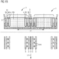
- the views of Figures 1B and 1F illustrate power semiconductor devices 1 embodied as cells being arranged laterally beside one another.
- the power semiconductor device 1 comprises a semiconductor body 2 extending in a vertical direction between an emitter side 21 with an emitter electrode 51 and a collector side 22 opposite the emitter side 21.
- the power semiconductor device 1 comprises a drift layer 26 of a first conductivity type, a base layer 28 of a second conductivity type different than the first conductivity type extending between the drift layer 26 and the emitter side 21.
- a source region 29 of the first conductivity type is arranged on a side of the base layer 28 that faces away from the drift layer 26.
- the first conductivity type is n-type and the second conductivity type is p-type so that the base layer 28 is a p-type layer.
- the layers may also be inverted with respect to their conductivity type.
- the power semiconductor device 1 comprises a first trench 3 and a second trench 4.
- the first trench 3 and the second trench 4 extend from the emitter side 21 into the drift layer 26.
- An insulated trench gate electrode 30 comprising a gate electrode layer 31 which is electrically conductive and a gate insulation layer 32 extends into the first trench 3.
- the gate electrode layer 31 is electrically insulated from the semiconductor body 2.
- the first trench 3 represents an active trench at the potential level of the gate voltage.
- the second trench 4 is arranged on a side of the first trench 3 facing away from the source region 29 and does not represent an active trench.
- An electrically conductive layer 41 extends into the second trench 4.
- the electrically conductive layer 41 is electrically insulated from the drift layer 26 and the base layer 28.
- the emitter electrode 51 is arranged at the emitter side 21.
- the first trench 3 and the second trench 4 may have the same depth, so that they can be formed in a common process step.
- the second trench 4 is electrically insulated from the insulated trench gate electrode 30 and is electrically connected to the emitter electrode 51.
- the electrically conductive layer 41 may also be electrically separated from the emitter electrode 51.
- the electrically conductive layer 41 is at the same voltage as the emitter electrode 51 or at a positive voltage with respect to the emitter electrode 51 during operation of the power semiconductor device 1.
- the electrically conductive layer 41 is at the voltage applied to the emitter electrode or at the voltage applied to the insulated trench gate electrode 3.
- the applied voltage may also differ from both the voltage at the insulated trench gate electrode 3 and the voltage at the emitter electrode.
- a positive voltage applied to the electrically conductive layer 41 may provide an improved electrostatic shielding of the sub-region 6.
- the emitter electrode 51 electrically contacts the base layer 28 laterally beside the source region 29 in a recess of the semiconductor body 2 formed in the emitter side 21.
- the emitter electrode 51 directly adjoins the source region 29 and a contact portion 282 of the base layer 28 which is more heavily doped than the rest of the base layer 28.
- the emitter electrode 51 may also be provided on the emitter side 21.
- the base layer 28 On a side of the second trench 4 that faces away from the first trench 3 the base layer 28 comprises a portion 281 having a depth d2 which is larger than or at least as large as a depth d1 of the second trench 4.
- the portion 281 of the base layer 28 extends from the emitter side 21 deeper in the vertical direction towards the collector side 22 than the second trench 4.
- the difference d2 - d1 is between 0 ⁇ m and 5 ⁇ m inclusive.
- the portion 281 directly adjoins a bottom of the second trench 4 in regions.
- a sub-region 6 of the power semiconductor device 1 extending between the first trench 3 and the second trench 4 comprises a charge carrier extraction contact 61 via which the base layer 28 is electrically connected.
- the sub-region 6 and the source region 29 are arranged on opposite sides of the first trench 3, so that the sub-region 6 is free of a source region.
- the charge carrier extraction contact 61 is electrically connected to the emitter electrode 51.
- the charge carrier extraction contact 61 may be at the emitter voltage Ve.
- the charge carrier extraction contact 61 may also be electrically addressable separately from the emitter electrode 51.
- the applied voltage may be independent from the voltage at the emitter electrode 51.
- the voltage applied to the charge carrier extraction contact 61 is positive with respect to the emitter electrode 51 or the same as the voltage at the emitter electrode 51.
- the voltage at the charge carrier extraction contact 61 differs for different states during operation.
- the second trench 4 acting as a dummy trench together with the portion 281 of the base layer 28 that extends deeper towards the collector side 22 than the second trench 4 results in a significant reduction of the avalanche generation during the turn-off switching of the power semiconductor device 1.
- Degradation of the gate insulation layer 32 caused by hot carriers may be eliminated or at least reduced in this manner.
- the reduced avalanche generation near the first trench 3 has been confirmed by simulations as illustrated in Figure 2A , comparing the time integrated avalanche generation per square centimetre during a turn-off switching near the first trench 3 for the power semiconductor device 1 with a first reference design R1 illustrated in Figure 2B and a second reference design R2 illustrated in Figure 2C .
- the reference design R1 only includes an active trench corresponding to the first trench 3 but no inactive trench.
- the reference design R2 includes an additional electrically inactive second trench 4.
- the base layer 28 has a continuous depth so that the depth of the base layer 28 is the same on both sides of the second trench 4.
- Figure 2A illustrates simulation results for two options for the second reference design R2 and the power semiconductor device 1 wherein in each case the bar on the left-hand side shows the time integrated avalanche generation A during a turn-off switching near the first trench 3 for a design without a charge carrier extraction contact whereas the bar on the right-hand side shows the results for a design with a charge carrier extraction contact 61.
- the time integrated avalanche generation A may be reduced by more than one order of magnitude compared to the reference design R2 and by two orders of magnitude with respect to the reference design R1 for the designs without a charge carrier extraction contact.
- the addition of the charge carrier extraction contact 61 results in a further reduction by two orders of magnitude.
- Figure 3A shows simulation results for a power semiconductor device 1 as described in Figure 1A in a bar diagram wherein bars 71 and 72 show the time integrated avalanche generation A near the first trench 3 (bar 71) and near the second trench 4 (bar 72) for a design without a charge carrier extraction contact 61.
- the bars 73 and 74 show corresponding simulation results with a charge carrier extraction contact 61.
- Figure 3B further shows simulation results for the time integrated avalanche generation A for a power semiconductor device as described in connection with Figure 1A as a function of an edge-to-edge distance s1 between the first trench 3 and the second trench 4
- curve 75 refers to a design without a charge carrier extraction contact
- curve 76 refers to a design with a charge carrier extraction contact 61.
- Curves 75 and 76 each refer to the avalanche generation near the first trench 3.
- Curve 77 shows the ratio R of the avalanche generation A between a region near the second trench 4 and near the first trench 3.
- the avalanche generation A decreases with decreasing edge-to-edge distance s1.
- the ratio R increases with decreasing edge-to-edge distance s1.
- the power semiconductor device 1 further comprises a collector layer 25.
- the collector layer 25 is of the second conductivity type.
- a collector electrode 52 is arranged on the collector side 22 of the power semiconductor device 1. The collector electrode 52 directly adjoins the collector layer 25.
- the power semiconductor device 1 is shown in the cross-sectional views for the sake of easier representation.
- the power semiconductor device 1 further comprises an optional enhancement layer 27 arranged between the drift layer 26 and the base layer 28 in regions.
- the enhancement layer 27 is a layer with a maximum doping concentration which is higher than the doping concentration of the drift layer 26 by at least a factor of 50.
- the enhancement layer 27 may act as a charge carrier barrier, for instance as a hole barrier for an n-type enhancement layer 27.
- the enhancement layer 27 is also present in the sub-region 6 so that the enhancement layer 27 reduces the charge carrier extraction at the charge carrier extraction contact 61, thereby reducing the on-state losses.
- the charge carrier extraction contact 61 still provides an additional escape path to the plasma during turn-off switching but at the same time limits the on-state losses due to the electrostatic screening of the sub-region 6 provided by the first trench 3 and the second trench 4.
- typical maximum doping concentrations may be between 1*10 12 cm -3 and 1*10 14 cm -3 for an n - drift layer 26, 3*10 16 cm -3 for an n enhancement layer 27, 1.5*10 17 cm -3 for a p base layer 28, 5*10 17 cm-3 for the portion 281 of the base layer 28 and 1*10 19 cm -3 for a p + contact portion 282 of the base layer 28.
- the power semiconductor device 1 comprises two partial regions 39 of the first trench 3 and two partial regions 49 of the second trench 4 wherein the two partial regions 49 of the second trench 4 are arranged between the two partial regions 39 of the first trench 3 in a cross-sectional view perpendicular to a main extension direction L1 of the first trench 3.
- the portion 281 of the base layer 28 having the depth d2 larger than the depth d1 of the second trenches 4 is formed between the two partial regions 49 of the second trench 4.
- the partial regions 49 of the second trench 4 may be formed by one contiguous second trench 4.
- the second trench 4 is formed as a closed loop when seen onto the emitter side 21.
- the partial regions 39 of the first trench 3 may be formed by one contiguous first trench 3.
- the second trench 4 is formed as a closed loop when seen onto the emitter side 21.
- the portion 281 of the base layer 28 is located completely within the closed loop formed by the second trench 4 when seen in vertical direction.
- partial regions 39 of the first trench 3 and/or the partial regions 49 of the second trenches 4 may also be formed by separate trenches in other designs.
- Figure 1F further shows a gate connector 35 electrically connecting the gate electrode layer 31 in the first trenches 3 of the cells to a gate potential and a connector 45 electrically connecting the electrically conductive layer 41 in the second trenches 4 of the cells to an emitter potential Ve.
- the connector 45 may also be used to connect the electrically conductive layer 41 to another potential.
- the charge carrier extraction contact 61 may be divided into a plurality of segments 610.
- the average center-to-center spacing between the segments 610 and their extension in a direction running in parallel to the main extension direction L1 may be varied within wide limits.
- the extension in the direction running in parallel to the main extension direction L1 is at least 0.1 % or at least 10 % or at least 20 % and/or at most 95 % or at most 80 %, for instance between 30 % and 50 % inclusive.
- the number of segments 610 amounts to between 20 and 200 per millimeter in a direction parallel to the main extension direction L1.
- a single segment may also be used instead.
- the power semiconductor device 1 has a cell design providing a stripe trench IGBT with a length of between 0.5 and 3 mm along the main extension direction L1.
- a cell pitch c1 i.e. a center-to-center distance between adjacent power semiconductor devices 1 in a direction perpendicular to the main extension direction L1 as illustrated in Figure 1B is between 10 ⁇ m and 500 ⁇ m inclusive, for example.
- the proposed design may also apply for other power semiconductor devices and other design geometries.
- the portion 281 extends below the second trench 4 in a direction towards the first trench 3.
- the second trench 4 completely overlaps with the portion when seen in vertical direction.
- the portion 281 extends beyond the second trench 4 when seen towards the first trench 3, but does not overlap with the charge carrier extraction contact 61 when seen in vertical direction. This is illustrated using line 62 referring to the edge of the charge carrier extraction contact 61 at the side facing the second trench 4.
- the portion 281 may extend even further towards the first trench 3.
- the sub-region 6 completely overlaps with the portion 281 when seen in vertical direction.
- the sub-region 281 may be completely of the second conductivity type.
- a part of the drift layer 26 and/or a part of the enhancement layer 27 may be located on a side of the portion 281 that faces the emitter side 21.
- first trench 3 may overlap in regions or completely with the portion 281 when seen in vertical direction.
Landscapes
- Electrodes Of Semiconductors (AREA)
- Metal-Oxide And Bipolar Metal-Oxide Semiconductor Integrated Circuits (AREA)
Priority Applications (6)
| Application Number | Priority Date | Filing Date | Title |
|---|---|---|---|
| EP20216115.4A EP4016638A1 (fr) | 2020-12-21 | 2020-12-21 | Dispositif semi-conducteur de puissance à électrode à grille de tranchée isolée |
| PCT/EP2021/086590 WO2022136179A1 (fr) | 2020-12-21 | 2021-12-17 | Dispositif à semi-conducteur de puissance doté d'électrode de grille à tranchée isolée et procédé de production de dispositif à semi-conducteur de puissance |
| US18/268,804 US20240038879A1 (en) | 2020-12-21 | 2021-12-17 | Power semiconductor device with an insulated trench gate electrode and method of producing a power semiconductor device |
| JP2023537636A JP2024501237A (ja) | 2020-12-21 | 2021-12-17 | 絶縁トレンチゲート電極を有するパワー半導体デバイスおよびパワー半導体デバイスを製造する方法 |
| CN202180085877.3A CN116636012A (zh) | 2020-12-21 | 2021-12-17 | 具有绝缘沟槽栅电极的功率半导体器件和生产功率半导体器件的方法 |
| DE212021000529.2U DE212021000529U1 (de) | 2020-12-21 | 2021-12-17 | Leistungshalbleitervorrichtung mit isolierter Graben-Gate-Elektrode |
Applications Claiming Priority (1)
| Application Number | Priority Date | Filing Date | Title |
|---|---|---|---|
| EP20216115.4A EP4016638A1 (fr) | 2020-12-21 | 2020-12-21 | Dispositif semi-conducteur de puissance à électrode à grille de tranchée isolée |
Publications (1)
| Publication Number | Publication Date |
|---|---|
| EP4016638A1 true EP4016638A1 (fr) | 2022-06-22 |
Family
ID=73856430
Family Applications (1)
| Application Number | Title | Priority Date | Filing Date |
|---|---|---|---|
| EP20216115.4A Pending EP4016638A1 (fr) | 2020-12-21 | 2020-12-21 | Dispositif semi-conducteur de puissance à électrode à grille de tranchée isolée |
Country Status (6)
| Country | Link |
|---|---|
| US (1) | US20240038879A1 (fr) |
| EP (1) | EP4016638A1 (fr) |
| JP (1) | JP2024501237A (fr) |
| CN (1) | CN116636012A (fr) |
| DE (1) | DE212021000529U1 (fr) |
| WO (1) | WO2022136179A1 (fr) |
Cited By (4)
| Publication number | Priority date | Publication date | Assignee | Title |
|---|---|---|---|---|
| CN116230760A (zh) * | 2023-02-23 | 2023-06-06 | 成都森未科技有限公司 | 一种沟槽栅型igbt |
| EP4394888A1 (fr) * | 2022-12-30 | 2024-07-03 | Hitachi Energy Ltd | Dispositif semi-conducteur et procédé de fabrication d'un dispositif semi-conducteur |
| EP4394881A1 (fr) * | 2022-12-30 | 2024-07-03 | Hitachi Energy Ltd | Dispositif semi-conducteur et procédé de fabrication d'un dispositif semi-conducteur |
| EP4394889A1 (fr) * | 2022-12-30 | 2024-07-03 | Hitachi Energy Ltd | Dispositif semi-conducteur et procédé de fabrication d'un dispositif semi-conducteur |
Citations (7)
| Publication number | Priority date | Publication date | Assignee | Title |
|---|---|---|---|---|
| DE19722441A1 (de) * | 1996-06-11 | 1997-12-18 | Mitsubishi Electric Corp | Halbleitervorrichtung und Verfahren zur Herstellung derselben |
| EP2613356A2 (fr) * | 2012-01-05 | 2013-07-10 | Renesas Electronics Corporation | IGBT à grille de tranchée de type IE |
| EP2942816A1 (fr) * | 2013-08-15 | 2015-11-11 | Fuji Electric Co., Ltd. | Dispositif à semi-conducteurs |
| US20170033206A1 (en) * | 2015-07-30 | 2017-02-02 | Renesas Electronics Corporation | Semiconductor device |
| US9825158B2 (en) | 2013-11-29 | 2017-11-21 | Abb Schweiz Ag | Insulated gate bipolar transistor |
| EP3340311A1 (fr) * | 2016-12-22 | 2018-06-27 | Renesas Electronics Corporation | Transistor bipolaire à grille isolée à tranchée |
| US20200006539A1 (en) | 2017-04-04 | 2020-01-02 | Infineon Technologies Ag | IGBT Having a Barrier Region |
Family Cites Families (7)
| Publication number | Priority date | Publication date | Assignee | Title |
|---|---|---|---|---|
| WO2011111500A1 (fr) * | 2010-03-09 | 2011-09-15 | 富士電機システムズ株式会社 | Dispositif semi-conducteur |
| JP5621703B2 (ja) * | 2011-04-26 | 2014-11-12 | 三菱電機株式会社 | 半導体装置 |
| JP6353804B2 (ja) * | 2015-03-27 | 2018-07-04 | 株式会社 日立パワーデバイス | 半導体装置及びそれを用いた電力変換装置 |
| JP2017174923A (ja) * | 2016-03-23 | 2017-09-28 | ルネサスエレクトロニクス株式会社 | 半導体装置 |
| JP6673501B2 (ja) * | 2016-12-08 | 2020-03-25 | 富士電機株式会社 | 半導体装置 |
| DE102017129955B4 (de) * | 2017-12-14 | 2021-10-07 | Infineon Technologies Austria Ag | Halbleitervorrichtung mit einem barrierengebiet sowie elektrische vorrichtung |
| JP7125339B2 (ja) * | 2018-12-26 | 2022-08-24 | ルネサスエレクトロニクス株式会社 | 半導体装置およびその製造方法 |
-
2020
- 2020-12-21 EP EP20216115.4A patent/EP4016638A1/fr active Pending
-
2021
- 2021-12-17 CN CN202180085877.3A patent/CN116636012A/zh active Pending
- 2021-12-17 JP JP2023537636A patent/JP2024501237A/ja active Pending
- 2021-12-17 WO PCT/EP2021/086590 patent/WO2022136179A1/fr not_active Ceased
- 2021-12-17 DE DE212021000529.2U patent/DE212021000529U1/de active Active
- 2021-12-17 US US18/268,804 patent/US20240038879A1/en active Pending
Patent Citations (7)
| Publication number | Priority date | Publication date | Assignee | Title |
|---|---|---|---|---|
| DE19722441A1 (de) * | 1996-06-11 | 1997-12-18 | Mitsubishi Electric Corp | Halbleitervorrichtung und Verfahren zur Herstellung derselben |
| EP2613356A2 (fr) * | 2012-01-05 | 2013-07-10 | Renesas Electronics Corporation | IGBT à grille de tranchée de type IE |
| EP2942816A1 (fr) * | 2013-08-15 | 2015-11-11 | Fuji Electric Co., Ltd. | Dispositif à semi-conducteurs |
| US9825158B2 (en) | 2013-11-29 | 2017-11-21 | Abb Schweiz Ag | Insulated gate bipolar transistor |
| US20170033206A1 (en) * | 2015-07-30 | 2017-02-02 | Renesas Electronics Corporation | Semiconductor device |
| EP3340311A1 (fr) * | 2016-12-22 | 2018-06-27 | Renesas Electronics Corporation | Transistor bipolaire à grille isolée à tranchée |
| US20200006539A1 (en) | 2017-04-04 | 2020-01-02 | Infineon Technologies Ag | IGBT Having a Barrier Region |
Cited By (7)
| Publication number | Priority date | Publication date | Assignee | Title |
|---|---|---|---|---|
| EP4394888A1 (fr) * | 2022-12-30 | 2024-07-03 | Hitachi Energy Ltd | Dispositif semi-conducteur et procédé de fabrication d'un dispositif semi-conducteur |
| EP4394881A1 (fr) * | 2022-12-30 | 2024-07-03 | Hitachi Energy Ltd | Dispositif semi-conducteur et procédé de fabrication d'un dispositif semi-conducteur |
| EP4394889A1 (fr) * | 2022-12-30 | 2024-07-03 | Hitachi Energy Ltd | Dispositif semi-conducteur et procédé de fabrication d'un dispositif semi-conducteur |
| WO2024141212A1 (fr) * | 2022-12-30 | 2024-07-04 | Hitachi Energy Ltd | Dispositif à semi-conducteur et procédé de production d'un dispositif à semi-conducteur |
| WO2024141238A1 (fr) * | 2022-12-30 | 2024-07-04 | Hitachi Energy Ltd | Dispositif à semi-conducteur et procédé de production d'un dispositif à semi-conducteur |
| WO2024141239A1 (fr) * | 2022-12-30 | 2024-07-04 | Hitachi Energy Ltd | Dispositif à semi-conducteur et procédé de production d'un dispositif à semi-conducteur |
| CN116230760A (zh) * | 2023-02-23 | 2023-06-06 | 成都森未科技有限公司 | 一种沟槽栅型igbt |
Also Published As
| Publication number | Publication date |
|---|---|
| WO2022136179A1 (fr) | 2022-06-30 |
| JP2024501237A (ja) | 2024-01-11 |
| CN116636012A (zh) | 2023-08-22 |
| US20240038879A1 (en) | 2024-02-01 |
| DE212021000529U1 (de) | 2023-12-01 |
Similar Documents
| Publication | Publication Date | Title |
|---|---|---|
| US11094808B2 (en) | Semiconductor device | |
| EP4016638A1 (fr) | Dispositif semi-conducteur de puissance à électrode à grille de tranchée isolée | |
| EP3659180B1 (fr) | Dispositif semi-conducteur à grille isolée et son procédé de fabrication | |
| EP3631862B1 (fr) | Dispositif semi-conducteur | |
| US20230071170A1 (en) | Semiconductor device | |
| EP1266406B1 (fr) | Transistor à effet de champ DMOS à grille en tranchée | |
| JP2013080796A (ja) | 半導体装置 | |
| KR101933235B1 (ko) | 전력 반도체 디바이스 | |
| US8067797B2 (en) | Variable threshold trench IGBT with offset emitter contacts | |
| US6147381A (en) | Field effect-controllable semiconductor component | |
| EP3154091A1 (fr) | Dispositif semi-conducteur à conduction inversée | |
| US11145717B2 (en) | Cellular insulated gate power device with edge design to prevent failure near edge | |
| KR20150069117A (ko) | 전력 반도체 소자 | |
| CN120091612A (zh) | 半导体结构元件和用于制造半导体结构元件的方法 | |
| EP3881360B1 (fr) | Transistor bipolaire à porte isolée | |
| EP1276156A1 (fr) | Transistor bipolaire à haute puissance | |
| US20250374574A1 (en) | Semiconductor device | |
| EP4203069B1 (fr) | Dispositif à semi-conducteur de puissance et procédé de fabrication | |
| EP4394881B1 (fr) | Dispositif semi-conducteur et procédé de fabrication d'un dispositif semi-conducteur | |
| US11610987B2 (en) | NPNP layered MOS-gated trench device having lowered operating voltage | |
| EP4187615A1 (fr) | Dispositif de tranchée à grille mos en couches npn ayant une tension de fonctionnement abaissée | |
| EP4394889A1 (fr) | Dispositif semi-conducteur et procédé de fabrication d'un dispositif semi-conducteur | |
| GB2592928A (en) | Insulated gate switched transistor | |
| CN119277800B (zh) | Igbt结构及半导体器件 | |
| EP4394888A1 (fr) | Dispositif semi-conducteur et procédé de fabrication d'un dispositif semi-conducteur |
Legal Events
| Date | Code | Title | Description |
|---|---|---|---|
| PUAI | Public reference made under article 153(3) epc to a published international application that has entered the european phase |
Free format text: ORIGINAL CODE: 0009012 |
|
| STAA | Information on the status of an ep patent application or granted ep patent |
Free format text: STATUS: THE APPLICATION HAS BEEN PUBLISHED |
|
| AK | Designated contracting states |
Kind code of ref document: A1 Designated state(s): AL AT BE BG CH CY CZ DE DK EE ES FI FR GB GR HR HU IE IS IT LI LT LU LV MC MK MT NL NO PL PT RO RS SE SI SK SM TR |
|
| STAA | Information on the status of an ep patent application or granted ep patent |
Free format text: STATUS: REQUEST FOR EXAMINATION WAS MADE |
|
| 17P | Request for examination filed |
Effective date: 20221213 |
|
| RBV | Designated contracting states (corrected) |
Designated state(s): AL AT BE BG CH CY CZ DE DK EE ES FI FR GB GR HR HU IE IS IT LI LT LU LV MC MK MT NL NO PL PT RO RS SE SI SK SM TR |
|
| P01 | Opt-out of the competence of the unified patent court (upc) registered |
Effective date: 20230527 |
|
| RAP1 | Party data changed (applicant data changed or rights of an application transferred) |
Owner name: HITACHI ENERGY LTD |
|
| RIN1 | Information on inventor provided before grant (corrected) |
Inventor name: CORVASCE, CHIARA Inventor name: BUITRAGO, ELIZABETH Inventor name: VITALE, WOLFGANG AMADEUS Inventor name: GUPTA, GAURAV Inventor name: DE MICHIELIS, LUCA |
|
| STAA | Information on the status of an ep patent application or granted ep patent |
Free format text: STATUS: EXAMINATION IS IN PROGRESS |
|
| 17Q | First examination report despatched |
Effective date: 20250617 |
|
| RIN1 | Information on inventor provided before grant (corrected) |
Inventor name: DE MICHIELIS, LUCA Inventor name: GUPTA, GAURAV Inventor name: VITALE, WOLFGANG AMADEUS Inventor name: BUITRAGO, ELIZABETH Inventor name: CORVASCE, CHIARA |