EP4016732A1 - Wellenleiter mit schlitzgespeisten dipolelementen - Google Patents
Wellenleiter mit schlitzgespeisten dipolelementen Download PDFInfo
- Publication number
- EP4016732A1 EP4016732A1 EP21211168.6A EP21211168A EP4016732A1 EP 4016732 A1 EP4016732 A1 EP 4016732A1 EP 21211168 A EP21211168 A EP 21211168A EP 4016732 A1 EP4016732 A1 EP 4016732A1
- Authority
- EP
- European Patent Office
- Prior art keywords
- waveguide
- dipole elements
- radiation
- radiation slots
- hollow channel
- Prior art date
- Legal status (The legal status is an assumption and is not a legal conclusion. Google has not performed a legal analysis and makes no representation as to the accuracy of the status listed.)
- Withdrawn
Links
- 230000005855 radiation Effects 0.000 claims abstract description 129
- 239000002184 metal Substances 0.000 claims description 5
- 229910052751 metal Inorganic materials 0.000 claims description 5
- 239000004033 plastic Substances 0.000 claims description 4
- 239000000758 substrate Substances 0.000 claims description 4
- 239000010410 layer Substances 0.000 description 79
- 238000000034 method Methods 0.000 description 16
- 239000004020 conductor Substances 0.000 description 4
- 230000005670 electromagnetic radiation Effects 0.000 description 4
- 238000004519 manufacturing process Methods 0.000 description 4
- 230000008901 benefit Effects 0.000 description 2
- 239000012141 concentrate Substances 0.000 description 2
- 239000000463 material Substances 0.000 description 2
- 239000002356 single layer Substances 0.000 description 2
- 229920000049 Carbon (fiber) Polymers 0.000 description 1
- RYGMFSIKBFXOCR-UHFFFAOYSA-N Copper Chemical compound [Cu] RYGMFSIKBFXOCR-UHFFFAOYSA-N 0.000 description 1
- BQCADISMDOOEFD-UHFFFAOYSA-N Silver Chemical compound [Ag] BQCADISMDOOEFD-UHFFFAOYSA-N 0.000 description 1
- 230000004888 barrier function Effects 0.000 description 1
- 239000004917 carbon fiber Substances 0.000 description 1
- 238000010276 construction Methods 0.000 description 1
- 229910052802 copper Inorganic materials 0.000 description 1
- 239000010949 copper Substances 0.000 description 1
- 238000001514 detection method Methods 0.000 description 1
- 238000005516 engineering process Methods 0.000 description 1
- 239000011152 fibreglass Substances 0.000 description 1
- PCHJSUWPFVWCPO-UHFFFAOYSA-N gold Chemical compound [Au] PCHJSUWPFVWCPO-UHFFFAOYSA-N 0.000 description 1
- 229910052737 gold Inorganic materials 0.000 description 1
- 239000010931 gold Substances 0.000 description 1
- LQBJWKCYZGMFEV-UHFFFAOYSA-N lead tin Chemical compound [Sn].[Pb] LQBJWKCYZGMFEV-UHFFFAOYSA-N 0.000 description 1
- VNWKTOKETHGBQD-UHFFFAOYSA-N methane Chemical compound C VNWKTOKETHGBQD-UHFFFAOYSA-N 0.000 description 1
- 238000012544 monitoring process Methods 0.000 description 1
- 229910052709 silver Inorganic materials 0.000 description 1
- 239000004332 silver Substances 0.000 description 1
- 239000011343 solid material Substances 0.000 description 1
- 239000002023 wood Substances 0.000 description 1
Images


Classifications
-
- H—ELECTRICITY
- H01—ELECTRIC ELEMENTS
- H01P—WAVEGUIDES; RESONATORS, LINES, OR OTHER DEVICES OF THE WAVEGUIDE TYPE
- H01P3/00—Waveguides; Transmission lines of the waveguide type
-
- H—ELECTRICITY
- H01—ELECTRIC ELEMENTS
- H01Q—ANTENNAS, i.e. RADIO AERIALS
- H01Q21/00—Antenna arrays or systems
- H01Q21/0006—Particular feeding systems
- H01Q21/0037—Particular feeding systems linear waveguide fed arrays
- H01Q21/0043—Slotted waveguides
-
- H—ELECTRICITY
- H01—ELECTRIC ELEMENTS
- H01P—WAVEGUIDES; RESONATORS, LINES, OR OTHER DEVICES OF THE WAVEGUIDE TYPE
- H01P3/00—Waveguides; Transmission lines of the waveguide type
- H01P3/12—Hollow waveguides
-
- H—ELECTRICITY
- H01—ELECTRIC ELEMENTS
- H01P—WAVEGUIDES; RESONATORS, LINES, OR OTHER DEVICES OF THE WAVEGUIDE TYPE
- H01P3/00—Waveguides; Transmission lines of the waveguide type
- H01P3/16—Dielectric waveguides, i.e. without a longitudinal conductor
-
- H—ELECTRICITY
- H01—ELECTRIC ELEMENTS
- H01Q—ANTENNAS, i.e. RADIO AERIALS
- H01Q1/00—Details of, or arrangements associated with, antennas
- H01Q1/27—Adaptation for use in or on movable bodies
- H01Q1/32—Adaptation for use in or on road or rail vehicles
- H01Q1/3208—Adaptation for use in or on road or rail vehicles characterised by the application wherein the antenna is used
- H01Q1/3233—Adaptation for use in or on road or rail vehicles characterised by the application wherein the antenna is used particular used as part of a sensor or in a security system, e.g. for automotive radar, navigation systems
-
- H—ELECTRICITY
- H01—ELECTRIC ELEMENTS
- H01Q—ANTENNAS, i.e. RADIO AERIALS
- H01Q13/00—Waveguide horns or mouths; Slot antennas; Leaky-waveguide antennas; Equivalent structures causing radiation along the transmission path of a guided wave
- H01Q13/02—Waveguide horns
- H01Q13/0233—Horns fed by a slotted waveguide array
-
- H—ELECTRICITY
- H01—ELECTRIC ELEMENTS
- H01Q—ANTENNAS, i.e. RADIO AERIALS
- H01Q19/00—Combinations of primary active antenna elements and units with secondary devices, e.g. with quasi-optical devices, for giving the antenna a desired directional characteristic
- H01Q19/28—Combinations of primary active antenna elements and units with secondary devices, e.g. with quasi-optical devices, for giving the antenna a desired directional characteristic using a secondary device in the form of two or more substantially straight conductive elements
Definitions
- Some devices use electromagnetic signals to detect and track objects.
- the electromagnetic signals are transmitted and received using one or more antennas.
- the radiation pattern of an antenna may be characterized by gain or beamwidth, which indicates gain as a function of direction. Precisely controlling the radiation pattern can improve the application of a radar system. For example, many automotive applications require radar systems that provide a narrow beamwidth to detect objects within a particular field-of-view (e.g., in a travel path of the vehicle).
- a waveguide may be used to improve and control the radiation pattern of such devices.
- Such waveguide can include perforations or radiating slots to guide radiation near the antenna. These waveguides, however, can generate a wider beamwidth than that which is required or desired for many applications.
- An apparatus may include a waveguide for providing narrow coverage in an azimth plane.
- the waveguide includes a hollow channel containing a dielectric and an array of radiation slots through a surface that is operably connected with the dielectric.
- the waveguide includes an array of dipole elements positioned on or in the surface and offset from each longitudinal side of the array of radiation slots. The radiation slots and dipole elements configure the described waveguide to focus an antenna radiation pattern that supports a narrow beamwidth.
- Radar systems are a sensing technology that some automotive systems rely on to acquire information about the surrounding environment. Radar systems generally use an antenna to direct electromagnetic energy or signals being transmited or received. Such radar systems can use multiple antenna elements in an array to provide increased gain and directivity in comparison to the radiation pattern achievable with a single antenna element. Signals from the multiple antenna elements are combined with appropriate phases and weighted amplitudes to provide the desired radiation pattern.
- the waveguide generally includes an array of radiation slots representing apertures in the waveguide. Manufacturers may select the number and arrangement of the radiation slots to provide the desired phasing, combining, or splitting of electromagnetic energy. For example, the radiation slots are equally spaced in a waveguide surface along a propagation direction of the electromagnetic energy. This arrangement of radiating slots generally provides a wide radiation pattern with relatively uniform radiation in the azimuth plane.
- the waveguide includes dipole elements on two sides of each radiation slot for a narrower radiation pattern.
- the dipole elements are positioned on an outer surface of the waveguide.
- the dipole elements have an approximately rectangular shape.
- the dipole elements have an approximately circular shape, oval shape, C shape, T shape, or L shape in other implementations.
- the dipole elements can be sized and positioned relative to the array of radiation slots to generate a radiation pattern with a narrow beamwidth and higher gain within the desired field-of-view
- the described waveguide may be particularly advantageous for use in an automotive context, for example, detecting objects in a roadway in a travel path of a vehicle.
- the narrow beamwidth allows a radar system of the vehicle to detect objects in a particular field-of-view (e.g., immediately in front of the vehicle).
- a radar system placed near the front of a vehicle can use a narrow beamwidth to focus on detecting objects immediately in front of the vehicle instead of objects located toward a side of the vehicle.
- This example waveguide is just one example of the described techniques, apparatuses, and systems of a waveguide with slot-fed dipole elements. This document describes other examples and implementations.
- FIG. 1 illustrates an example environment 100 in which a radar system 102 with a waveguide 110 with slot-fed dipole elements 116 is used on a vehicle 104.
- the vehicle 104 may use the waveguide 110 to enable operations of the radar system 102 that is configured to determine a proximity, an angle, or a velocity of one or more objects 108 in the proximity of the vehicle 104.
- the vehicle 104 can represent other types of motorized vehicles (e.g., a motorcycle, a bus, a tractor, a semi-trailer truck, or construction equipment), non-motorized vehicles (e.g., a bicycle), railed vehicles (e.g., a train or a trolley car), watercraft (e.g., a boat or a ship), aircraft (e.g., an airplane or a helicopter), or spacecraft (e.g., satellite).
- manufacturers can mount the radar system 102 to any moving platform, including moving machinery or robotic equipment.
- other devices e.g., desktop computers, tablets, laptops, televisions, computing watches, smartphones, gaming systems, and so forth
- the radar system 102 is mounted near, or integrated within, a front portion of the vehicle 104 to detect the object 108 and avoid collisions.
- the radar system 102 provides a field-of-view 106 towards the one or more objects 108.
- the radar system 102 can project the field-of-view 106 from any exterior surface of the vehicle 104.
- vehicle manufacturers can integrate the radar system 102 into a bumper, side mirror, headlights, rear lights, or any other interior or exterior location where the object 108 requires detection.
- the vehicle 104 includes multiple radar systems 102, such as a first radar system 102 and a second radar system 102 that provide a larger field-of-view 106.
- vehicle manufacturers can design the locations of the one or more radar systems 102 to provide a particular field-of-view 106 that encompasses a region of interest, including, for instance, in or around a travel lane aligned with a vehicle path.
- Example fields-of-view 106 include a 360-degree field-of-view, one or more 180-degree fields-of-view, one or more 90-degree fields-of-view, and so forth, which can overlap or be combined into a field-of-view 106 of a particular size.
- the described waveguide 110 includes dipole elements 116 to provide a radiation pattern with a narrower coverage in the azimuth plane and/or the elevation plane.
- a radar system placed near the front of a vehicle can use a narrow beamwidth to focus on detecting objects immediately in front of the vehicle (e.g., in a travel lane aligned with a vehicle path) instead of objects located toward a side of the vehicle (e.g., ahead of the vehicle 104 and in an adjacent travel lane to the vehicle path).
- the narrow coverage or narrow beamwidth can concentrate the radiated EM energy within plus or minus approximately 20 to 45 degrees of a direction following a travel path of the vehicle 104.
- a waveguide without the described configuration of dipole elements may provide a relatively uniform radiation pattern with the radiated EM energy within plus or minus approximately 75 degrees of the travel-path direction.
- the object 108 is composed of one or more materials that reflect radar signals. Depending on the application, the object 108 can represent a target of interest. In some cases, the object 108 can be a moving object or a stationary object.
- the stationary objects can be continuous (e.g., a concrete barrier, a guard rail) or discontinuous (e.g., a traffic cone) along a road portion.
- the radar system 102 emits electromagnetic radiation by transmitting one or more electromagnetic signals or waveforms via dipole elements 116.
- the radar system 102 can detect and track the object 108 by transmitting and receiving one or more radar signals.
- the radar system 102 can transmit electromagnetic signals between 100 and 400 gigahertz (GHz), between 4 and 100 GHz, or between approximately 70 and 80 GHz.
- GHz gigahertz
- the radar system 102 can determine a distance to the object 108 based on the time it takes for the signals to travel from the radar system 102 to the object 108 and from the object 108 back to the radar system 102.
- the radar system 102 can also determine the location of the object 108 in terms of an angle based on the direction of a maximum amplitude echo signal received by the radar system 102.
- the radar system 102 can be part of the vehicle 104.
- the vehicle 104 can also include at least one automotive system that relies on data from the radar system 102, including a driver-assistance system, an autonomous-driving system, or a semi-autonomous-driving system.
- the radar system 102 can include an interface to the automotive systems.
- the radar system 102 can output, via the interface, a signal based on electromagnetic energy received by the radar system 102.
- the automotive systems use radar data provided by the radar system 102 to perform a function.
- the driver-assistance system can provide blind-spot monitoring and generate an alert indicating a potential collision with the object 108 detected by the radar system 102.
- the radar data from the radar system 102 indicates when it is safe or unsafe to change lanes.
- the autonomous-driving system may move the vehicle 104 to a particular location on the road while avoiding collisions with the object 108 detected by the radar system 102.
- the radar data provided by the radar system 102 can provide information about a distance to and the location of the object 108 to enable the autonomous-driving system to perform emergency braking, perform a lane change, or adjust the speed of the vehicle 104.
- the radar system 102 generally includes a transmitter (not illustrated) and at least one antenna, including the waveguide 110, to transmit electromagnetic signals.
- the radar system 102 generally includes a receiver (not illustrated) and at least one antenna, including the waveguide 110, to receive reflected versions of these electromagnetic signals.
- the transmitter includes components for emitting electromagnetic signals.
- the receiver includes components to detect the reflected electromagnetic signals.
- the transmitter and the receiver can be incorporated together on the same integrated circuit (e.g., a transceiver integrated circuit) or separately on different integrated circuits.
- the radar system 102 also includes one or more processors (not illustrated) and computer-readable storage media (CRM) (not illustrated).
- the processor can be a microprocessor or a system-on-chip.
- the processor executes instructions stored within the CRM.
- the processor can control the operation of the transmitter.
- the processor can also process electromagnetic energy received by the antenna and determine the location of the object 108 relative to the radar system 102.
- the processor can also generate radar data for the automotive systems. For example, the processor can control, based on processed electromagnetic energy from the antenna, an autonomous or semi-autonomous driving system of the vehicle 104.
- the waveguide 110 includes at least one layer that can be any solid material, including wood, carbon fiber, fiber glass, metal, plastic, or a combination thereof.
- the waveguide 110 can also include a printed circuit board (PCB).
- the waveguide 110 is designed to mechanically support and electrically connect components (e.g., a waveguide channel 112, radiation slots 114, dipole elements 116) to a dielectric using conductive materials.
- the waveguide channel 112 includes a hollow channel to contain the dielectric (e.g., air).
- the radiation slots 114 provide an opening through a layer or surface of the waveguide 110.
- the radiation slots 114 are configured to allow electromagnetic energy to dissipate to the environment 100 from the dielectric in the waveguide channel 112.
- the dipole elements 116 are formed on the surface of the waveguide 110 and to the side of the radiation slots 114.
- the dipole elements 116 act as radiating elements for the electromagnetic energy dissipating through the radiation slots 114 and effectively concentrate the radiation pattern to a narrower field-of-view 106.
- the narrow beamwidth allows a radar system 102 of the vehicle 104 to detect objects 108 in a particular field-of-view 106 (e.g., immediately in front of the vehicle).
- a radar system 102 placed near the front of a vehicle 104 can use a narrow beamwidth in one plane (e.g., the azimuth plane) to focus on detecting objects 108 immediately in front of the vehicle 104 instead of objects located toward a side of the vehicle 104.
- FIG. 2 illustrates a top view 200 of a waveguide 202 with slot-fed dipole elements 116.
- the waveguide 202 is an example of the waveguide 110 of FIG. 1 .
- a cross-section view 210 of the waveguide 202 is illustrated in FIG. 3 .
- the waveguide 202 includes the waveguide channel 112, multiple radiation slots 114, and multiple dipole elements 116.
- the waveguide channel 112 is configured to channel electromagnetic signals transmitted by the transmitter and an antenna 204.
- the antenna 204 can be electrically coupled to a floor of the waveguide channel 112.
- the floor of the waveguide channel 112 is opposite a first layer 206, on which the dipole elements 116 are positioned.
- the waveguide channel 112 can include a hollow channel for a dielectric.
- the dielectric generally includes air, and the waveguide 202 is an air waveguide.
- the waveguide channel 112 forms an opening in a longitudinal direction 208 at one end of the waveguide 202 and a closed wall at an opposite end.
- the antenna 204 is electrically coupled to the dielectric via the floor of the waveguide channel 112. Electromagnetic signals enter the waveguide channel 112 through the opening and exit the waveguide channel 112 via the radiation slots 114.
- the waveguide channel 112 forms an approximately rectangular shape in the longitudinal direction 208.
- the waveguide channel 112 can also form a zigzag shape in the longitudinal direction 208.
- the radiation slots 114 provide an opening through the first layer 206 that defines a surface of the waveguide channel 112.
- the radiation slots 114 can have an approximately rectangular shape (e.g., a longitudinal slot parallel to the longitudinal direction 208) as illustrated in FIG. 2 .
- the longitudinal slots allow the radiation slots 114, in combination with the dipole elements 116, to produce a horizontal-polarized radiation pattern.
- the radiation slots 114 can have other shapes in other implementations, including approximately circular, oval, or square.
- the radiation slots 114 are sized and positioned on the first layer 206 to produce a particular radiation pattern for the antenna 204.
- at least some of the radiation slots 114 are offset from the longitudinal direction 208 (e.g., a centerline of the waveguide channel 112) by varying or non-uniform distances (e.g., in a zigzag shape) to reduce or eliminate side lobes from the radiation pattern of the waveguide 202.
- the radiation slots 114 nearer the wall at the opposite end of the waveguide channel 112 can have a larger longitudinal opening than the radiation slots 114 nearer the opening of the waveguide channel 112.
- the specific size and position of the radiation slots 114 can be determined by building and optimizing a model of the waveguide 202 to produce the desired radiation pattern.
- the plurality of radiation slots 114 is evenly distributed along the waveguide channel 112 between the opening of the waveguide channel and the closed wall.
- Each adjacent pair of radiation slots 114 are separated along the longitudinal direction 208 by a uniform distance to produce a particular radiation pattern.
- the uniform distance which is generally less than one wavelength of the electromagnetic radiation, can prevent grating lobes in the radiation pattern.
- the dipole elements 116 are formed on an outer surface of the first layer 206.
- the dipole elements 116 have an approximately rectangular shape in the depicted implementation.
- the dipole elements 116 can have an approximately circular shape, oval shape, C shape, T shape, or L shape in other implementations. In yet other implementations, the dipole elements 116 can combine the described shapes.
- a dipole element 116 is positioned adjacent to and offset from a longitudinal side of each radiation slot 114.
- the longitudinal sides of the radiation slots 114 are approximately parallel to the longitudinal direction 208.
- the dipole elements 116 can be offset a first distance from the longitudinal sides of the radiation slots 114 to generate a particular band of coverage in the radiation pattern of the antenna 204.
- the dipole elements 116 can also have a height that is less than the depth of the radiation slots 114.
- the electromagnetic radiation that leaks through the radiation slots 114 may excite the dipole elements 116 to generate a radiation pattern with a narrow beamwidth in the azimuth plane.
- the shape and size of the dipole elements 116 can be configured to vary the bandwidth and characteristics of the radiation pattern.
- the specific size and position of the dipole elements 116 can be determined by building and optimizing a model of the waveguide 202 to produce the desired radiation pattern.
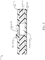
- FIG. 3 illustrates the cross-section view 210 of the waveguide 202 with slot-fed dipole elements.
- the waveguide 202 includes the first layer 206, a second layer 302, and a third layer 304.
- the first layer 206, the second layer 302, and the third layer 304 can be metal or metal-plated material.
- the radiation slots 114 form openings in the first layer 206 into the waveguide channel 112.
- the dipole elements 116 are formed on or as part of the first layer 206.
- the second layer 302 forms sides of the waveguide channel 112.
- the third layer 304 forms the floor of the waveguide channel 112.
- the first layer 206, the second layer 302, and the third layer 304 are separate layers.
- the first layer 206, the second layer 302, and the third layer 304 can be formed as a single layer that defines the waveguide channel 112, the radiation slots 114, and the dipole elements 116.
- the waveguide channel 112 can form an approximately rectangular opening in the cross-section view 210 of the waveguide 202. In other implementations, the waveguide channel 112 can form an approximately square, oval, or circular opening in the cross-section view 210 of the waveguide 202.
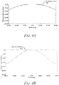
- FIG. 4A illustrates a radiation pattern 400 associated with an example waveguide without slot-fed dipole elements.
- the example waveguide without slot-fed dipole elements can generate a uniform radiation pattern 400 in an azimuth plane but with a relatively wide beamwidth.
- FIG. 4B illustrates a radiation pattern 410 associated with an example waveguide with slot-fed dipole elements.
- This generates a uniform radiation pattern 410, also in the azimuth plane, but with a relatively narrow beamwidth.
- the example waveguide can include the waveguide 202 illustrated in FIGs. 2 and 3 with the radiation slots 114 and the dipole elements 116.
- the waveguide 202 can generate the uniform radiation pattern 410 with the narrow beamwidth in the azimuth plane to enable a radar system to focus the radiation pattern of a corresponding antenna on a narrower field-of-view where potential objects-of-interest are located than the radar system can using the radiation pattern 400 illustrated in FIG. 4A .
- a radar system placed near the front of a vehicle can use a narrow beamwidth to focus on detecting objects immediately in front of the vehicle instead of objects located toward a side of the vehicle.
- FIG. 5A illustrates a top view 500 of a waveguide 504 with slot-fed dipole elements 116.
- FIG. 5B illustrates a cross-section view 502 of the waveguide 504.
- the waveguide 504 includes the waveguide channel 112, the radiation slots 114, and the dipole elements 116.
- the waveguide 504 includes a first layer 508, a second layer 510, a third layer 512, a fourth layer 514, and a fifth layer 516.
- the first layer 508, the second layer 510, and the third layer d512 provide a top conductive layer, a substrate layer, and a bottom conductive layer, respectively, of a printed circuit board (PCB).
- the first layer 508 and the third layer 512 can include various conductive materials, including tin-lead, silver, gold, copper, and so forth, to enable the transport of electromagnetic energy.
- the fourth layer 514 and the fifth layer 516 form sides and the floor, respectively, of the waveguide channel 112.
- the fourth layer 514 and the fifth layer 516 are separate layers in the depicted implementation. In other implementations, the fourth layer 514 and the fifth layer 516 can be formed as a single layer and combined with the PCB structure to form the waveguide channel 112.
- PCB structure for the waveguide 504 provides several advantages over the structure of the waveguide 202 illustrated in FIGs. 2 and 3 .
- using a PCB allows manufacturing of the waveguide 504 to be cheaper, less complicated, and easier for mass production.
- the PCB use provides low loss of electromagnetic radiation from the input of the waveguide channel 112 to radiation from the dipole elements 116.
- the first layer 508 can be etched to form the dipole elements 116 as part of the top conductive layer of the PCB.
- the third layer 512 can be etched to form the radiation slots 114 as part of the bottom conductive layer of the PCB.
- Via holes 506 provide a hole in the second layer 510 to electrically and mechanically connect the dipole elements 116 to the third layer 512.
- the via holes 506 illustrated in the top view 500 and the cross-section view 502 resemble a cylinder with a circular cross-section.
- the via holes 506 may include various shapes, including an approximately rectangular, oval, or square cross-section.
- the via holes 506 may also include various sizes (e.g., diameters).
- the via holes 506 are plated or filled with a conductive material, generally the same conductive material used for the first layer 508 and the third layer 512.
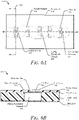
- FIG. 6A illustrates a top view 600 of a waveguide 604 with slot-fed dipole elements 116 and a zigzag waveguide channel 606.
- FIG. 6B illustrates a cross-section view 602 of the waveguide 604.
- the waveguide 604 includes the radiation slots 114, the dipole elements 116, and the via holes 506, similar to those illustrated for the waveguide 504 of FIGs. 5A and 5B .
- the waveguide 604 also includes the first layer 508, the second layer 510, the third layer 512, the fourth layer 514, and the fifth layer 516, similar to those illustrated for the waveguide 504 in FIGs. 5A and 5B .
- the first layer 508, the second layer 510, and the third layer 512 of the waveguide 604 provide a top conductive layer, a substrate layer, and a bottom conductive layer, respectively, of a printed circuit board (PCB).
- PCB printed circuit board
- the zigzag waveguide channel 606 forms a zigzag shape in the longitudinal direction 208.
- the zigzag shape of the zigzag waveguide channel 606 can reduce or eliminate grating lobes in the radiation pattern that a straight or rectangular waveguide shape can introduce (e.g., the waveguide channel 112).
- the turns in the zigzag shape can include various turning angles to provide the zigzag shape in the longitudinal direction 208.
- the turning angle of the zigzag waveguide is larger than 0 degree but less than 90 degrees.
- the zigzag waveguide channel 606 forms an approximately rectangular opening in the cross-section view 602 of the waveguide 604.
- the zigzag waveguide channel 606 can form an approximately square, oval, or circular opening in the cross-section view 602.
- the plurality of radiation slots 114 is evenly distributed along the zigzag waveguide channel 606 between the opening of the waveguide channel and the closed wall. Each adjacent pair of radiation slots 114 are separated along the longitudinal direction 208 by a uniform distance to produce a particular radiation pattern.
- the zigzag shape of the zigzag waveguide channel 606 allows manufacturers to position the radiation slots 114 in an approximately straight line along the longitudinal direction 208.
- the dipole elements 116 include an array of dipole elements 116 positioned on both longitudinal sides of the radiation slots 114.
- the dipole element 116 can include a single dipole element 116 positioned on both longitudinal sides of the radiation slots 114.
- the dipole elements 116 can include two approximately rectangular elements that extend lengthwise in the longitudinal direction from the radiation slot 114 nearest to the opening of the zigzag waveguide channel 606 to the radiation slot 114 nearest the closed end of the zigzag waveguide channel 606.
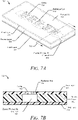
- FIG. 7A illustrates a perspective view 700 of a waveguide 704 with another example of slot-fed cavities 706 and the zigzag waveguide channel 606.
- FIG. 7B illustrates a cross-section view 702 of the waveguide 704.
- the waveguide 704 includes the radiation slots 114, the first layer 206, the second layer 302, and the third layer 304, similar to those illustrated for the waveguide 202 in FIGs. 1-3 .
- the waveguide 704 can include the first layer 508, the second layer 510, the third layer 512, the fourth layer 514, and the fifth layer 516, similar to those illustrated for the waveguide 504 in FIGs. 5A and 5B .
- the waveguide 704 also includes the zigzag waveguide channel 606, similar to that illustrated for the waveguide 604 in FIGs. 6A and 6B .
- the waveguide 704 can include an approximately rectangular waveguide channel similar to the waveguide channel 112 illustrated of the waveguide 202 of FIG. 2 .
- the cavities 706 are formed as recesses or cavities in the first layer 206.
- the cavity of the cavities 706 has an approximately rectangular shape.
- the cavities 706 can have an approximately circular shape, oval shape, C shape, T shape, or L shape in other implementations. In yet other implementations, the cavities 706 can combine the described shapes.
- a cavity 706 is positioned adjacent to and offset from a longitudinal side of each radiation slot 114.
- the cavities 706 include an array of cavities positioned on both longitudinal sides of the radiation slots 114.
- the cavities 706 can include a single cavity 706 positioned on both longitudinal sides of the radiation slots 114.
- the cavities 706 can include two approximately rectangular cavities that extend lengthwise in the longitudinal direction from the radiation slot 114 nearest to the opening of the zigzag waveguide channel 606 to the radiation slot 114 nearest the closed end of the zigzag waveguide channel 606.
- the cavities of the cavities 706 are sized and positioned to produce a radiation pattern with a narrow beamwidth.
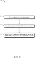
- FIG. 8 illustrates an example method 800 that can be used for manufacturing a waveguide with slot-fed dipole elements, following techniques, apparatuses, and systems of this disclosure.
- Method 800 is shown as sets of operations (or acts) performed, but not necessarily limited to the order or combinations in which the operations are shown herein. Further, any of one or more of the operations may be repeated, combined, or reorganized to provide other methods.
- reference may be made to the environment 100 of FIG. 1 and entities detailed in FIGs. 1 through 7 , reference to which is made for example only.
- the techniques are not limited to performance by one entity or multiple entities.
- a waveguide with slot-fed dipole elements is formed.
- the waveguide 110, 202, 504, 604, and/or 704 can be stamped, etched, cut, machined, cast, molded, or formed in some other way.
- the waveguide is integrated into a system.
- the waveguide 110, 202, 504, 604, and/or 704 is electrically coupled to the antenna 204.
- electromagnetic signals are received or transmitted via the waveguide at or by an antenna of the system, respectively.
- the antenna 204 receives or transmits signals captured via the waveguide 110, 202, 504, 604, and/or 704 and routed through the radar system 102.
- Example 1 An apparatus comprising: a waveguide including a hollow channel for a dielectric, the hollow channel forming: a first opening in a longitudinal direction at one end of the waveguide; a closed wall at an opposite end of the waveguide; a plurality of radiation slots, each of the radiation slots comprising a second opening through a surface of the waveguide that defines the hollow channel, each of the radiation slots being operably connected with the dielectric; and a plurality of dipole elements positioned on or in the surface, one of the plurality of dipole elements positioned adjacent to and offset from each longitudinal side of each radiation slot of the plurality of radiation slots, each longitudinal side being parallel with the longitudinal direction through the hollow channel, the plurality of dipole elements and the plurality of radiation slots being arranged on the surface to produce a particular radiation pattern for an antenna element that is electrically coupled to the dielectric from a floor of the hollow channel.
- Example 2 The apparatus of example 1, wherein: the waveguide includes a printed circuit board (PCB) having a first conductive layer, a second substrate layer, and a third conductive layer, wherein: the plurality of radiation slots are formed in the third conductive layer of the PCB; and the plurality of dipole elements are formed in the first conductive layer of the PCB and operably connected, using via holes, to the third conductive layer.
- PCB printed circuit board
- Example 3 The apparatus of example 1 or 2, wherein each of the plurality of dipole elements is offset a first distance from each longitudinal side of each radiation slot, the first distance being selected to generate a particular band of coverage in the radiation pattern of the antenna element.
- Example 4 The apparatus of any one of examples 1 through 3, wherein each of the plurality of dipole elements has a height less than a depth of each of the plurality of radiation slots.
- Example 5 The apparatus of any one of examples 1 through 4, wherein the plurality of dipole elements have an approximately rectangular shape.
- Example 6 The apparatus of any one of examples 1 through 4, wherein the plurality of dipole elements have an approximately circular shape, oval shape, C shape, T shape, or L shape.
- Example 7 The apparatus of any one of examples 1 through 6, wherein the first opening comprises an approximately rectangular shape and the hollow channel forms an approximately rectangular shape along the longitudinal direction.
- Example 8 The apparatus of example 7, wherein the plurality of radiation slots are offset a non-uniform distance from a centerline of the hollow channel, the center line being parallel with the longitudinal direction.
- Example 9 The apparatus of any one of examples 1 through 6, wherein the first opening comprises an approximately rectangular shape and the hollow channel forms a zigzag shape along the longitudinal direction of the waveguide.
- Example 10 The apparatus of example 9, wherein the zigzag shape comprises multiple turns along the longitudinal direction, each of the multiple turns having a turning angle between 0 and 90 degrees.
- Example 12 The apparatus of example 11, wherein the plurality of dipole elements comprise two approximately rectangular dipole elements that extend along the longitudinal direction of the waveguide, the approximately rectangular dipole elements positioned adjacent to and offset from each longitudinal side of the plurality of radiation slots.
- Example 13 The apparatus of example 1, wherein the first opening comprises an approximately square shape, oval shape, or circular shape.
- Example 14 The apparatus of example 1, wherein the plurality of radiation slots is evenly distributed between the first opening and the closed wall along the longitudinal direction of the waveguide.
- Example 15 The apparatus of example 1, wherein the waveguide comprises metal.
- Example 16 The apparatus of example 1, wherein the waveguide comprises plastic.
- Example 17 The apparatus of example 1, wherein the dielectric comprises air and the waveguide is an air waveguide.
- Example 18 The apparatus of any one of examples 1 through 12, wherein: the plurality of radiation slots is evenly distributed between the first opening and the closed wall along the longitudinal direction of the waveguide; the waveguide comprises metal or plastic; and the dielectric comprises air and the waveguide is an air waveguide.
- Example 19 A system comprising: an antenna element; a device configured to transmit or receive electromagnetic signals via the antenna; and a waveguide including a hollow channel for a dielectric, the hollow channel forming: a first opening in a longitudinal direction at one end of the waveguide; a closed wall at an opposite end of the waveguide; a plurality of radiation slots, each of the radiation slots comprising a second opening through a surface of the waveguide that defines the hollow channel, each of the radiation slots being operably connected with the dielectric; and a plurality of dipole elements positioned on or in the surface, one of the plurality of dipole elements positioned adjacent to and offset from each longitudinal side of each radiation slot of the plurality of radiation slots, each longitudinal side being parallel with the longitudinal direction through the hollow channel, the plurality of dipole elements and the plurality of radiation slots being arranged on the surface to produce a particular radiation pattern for the antenna element that is electrically coupled to the dielectric from a floor of the hollow channel.
- Example 20 The system of example 19, wherein the device comprises a radar system.
- Example 21 The system of example 20, wherein the system is a vehicle.
- Example 22 A system comprising: an antenna element; a device configured to transmit or receive electromagnetic signals via the antenna; and a waveguide including a hollow channel for a dielectric, the hollow channel formed according to any one of examples 1 through 12 or 18.
- Example 23 The system of example 14, wherein: the device comprises a radar system; and the system is a vehicle.
Landscapes
- Engineering & Computer Science (AREA)
- Computer Security & Cryptography (AREA)
- Radar, Positioning & Navigation (AREA)
- Remote Sensing (AREA)
- Waveguide Aerials (AREA)
- Variable-Direction Aerials And Aerial Arrays (AREA)
- Radar Systems Or Details Thereof (AREA)
Applications Claiming Priority (5)
| Application Number | Priority Date | Filing Date | Title |
|---|---|---|---|
| US202063127873P | 2020-12-18 | 2020-12-18 | |
| US202063127819P | 2020-12-18 | 2020-12-18 | |
| US202063127861P | 2020-12-18 | 2020-12-18 | |
| US202163169062P | 2021-03-31 | 2021-03-31 | |
| US17/234,238 US20220200115A1 (en) | 2020-12-18 | 2021-04-19 | Waveguide with slot-fed dipole elements |
Publications (1)
| Publication Number | Publication Date |
|---|---|
| EP4016732A1 true EP4016732A1 (de) | 2022-06-22 |
Family
ID=78819430
Family Applications (1)
| Application Number | Title | Priority Date | Filing Date |
|---|---|---|---|
| EP21211168.6A Withdrawn EP4016732A1 (de) | 2020-12-18 | 2021-11-29 | Wellenleiter mit schlitzgespeisten dipolelementen |
Country Status (3)
| Country | Link |
|---|---|
| US (1) | US20220200115A1 (de) |
| EP (1) | EP4016732A1 (de) |
| CN (1) | CN114649658A (de) |
Cited By (1)
| Publication number | Priority date | Publication date | Assignee | Title |
|---|---|---|---|---|
| CN117855812A (zh) * | 2024-01-29 | 2024-04-09 | 中国科学院上海微系统与信息技术研究所 | 一种波导天线阵及通信模块 |
Families Citing this family (1)
| Publication number | Priority date | Publication date | Assignee | Title |
|---|---|---|---|---|
| US12586915B2 (en) * | 2024-08-19 | 2026-03-24 | Nxp B.V. | Antenna assembly with metallized cavity waveguide |
Citations (1)
| Publication number | Priority date | Publication date | Assignee | Title |
|---|---|---|---|---|
| US20160126637A1 (en) * | 2014-04-23 | 2016-05-05 | Fujikura Ltd. | Slotted waveguide array antenna and slotted array antenna module |
Family Cites Families (13)
| Publication number | Priority date | Publication date | Assignee | Title |
|---|---|---|---|---|
| US3328800A (en) * | 1964-03-12 | 1967-06-27 | North American Aviation Inc | Slot antenna utilizing variable standing wave pattern for controlling slot excitation |
| US3594806A (en) * | 1969-04-02 | 1971-07-20 | Hughes Aircraft Co | Dipole augmented slot radiating elements |
| GB1446416A (en) * | 1972-11-04 | 1976-08-18 | Marconi Co Ltd | Waveguide couplers |
| GB2463711B (en) * | 1987-03-31 | 2010-09-29 | Dassault Electronique | Double polarization flat array antenna |
| US5030965A (en) * | 1989-11-15 | 1991-07-09 | Hughes Aircraft Company | Slot antenna having controllable polarization |
| US6166701A (en) * | 1999-08-05 | 2000-12-26 | Raytheon Company | Dual polarization antenna array with radiating slots and notch dipole elements sharing a common aperture |
| US7498994B2 (en) * | 2006-09-26 | 2009-03-03 | Honeywell International Inc. | Dual band antenna aperature for millimeter wave synthetic vision systems |
| WO2009107216A1 (ja) * | 2008-02-28 | 2009-09-03 | 三菱電機株式会社 | 導波管スロットアレーアンテナ装置 |
| CN102420352A (zh) * | 2011-12-14 | 2012-04-18 | 佛山市健博通电讯实业有限公司 | 一种双极化天线 |
| JP2013187752A (ja) * | 2012-03-08 | 2013-09-19 | Mitsubishi Electric Corp | 導波管スロットアレーアンテナ装置 |
| US10852390B2 (en) * | 2017-12-20 | 2020-12-01 | Waymo Llc | Multiple polarization radar unit |
| CN109286081A (zh) * | 2018-08-03 | 2019-01-29 | 西安电子科技大学 | 基片集成波导馈电的宽带平面阵列天线 |
| US11349220B2 (en) * | 2020-02-12 | 2022-05-31 | Veoneer Us, Inc. | Oscillating waveguides and related sensor assemblies |
-
2021
- 2021-04-19 US US17/234,238 patent/US20220200115A1/en not_active Abandoned
- 2021-11-29 EP EP21211168.6A patent/EP4016732A1/de not_active Withdrawn
- 2021-12-17 CN CN202111550163.3A patent/CN114649658A/zh active Pending
Patent Citations (1)
| Publication number | Priority date | Publication date | Assignee | Title |
|---|---|---|---|---|
| US20160126637A1 (en) * | 2014-04-23 | 2016-05-05 | Fujikura Ltd. | Slotted waveguide array antenna and slotted array antenna module |
Non-Patent Citations (2)
| Title |
|---|
| ALHUWAIMEL SAAD ET AL: "Performance enhancement of a slotted waveguide antenna by utilizing parasitic elements", 2015 IEEE-APS TOPICAL CONFERENCE ON ANTENNAS AND PROPAGATION IN WIRELESS COMMUNICATIONS (APWC), IEEE, 7 September 2015 (2015-09-07), pages 1303 - 1306, XP032795007, DOI: 10.1109/APWC.2015.7300209 * |
| MAK KA-MING ET AL: "A Magnetoelectric Dipole Leaky-Wave Antenna for Millimeter-Wave Application", IEEE TRANSACTIONS ON ANTENNAS AND PROPAGATION, IEEE, USA, vol. 65, no. 12, 3 July 2017 (2017-07-03), pages 6395 - 6402, XP011673556, ISSN: 0018-926X, [retrieved on 20171128], DOI: 10.1109/TAP.2017.2722868 * |
Cited By (1)
| Publication number | Priority date | Publication date | Assignee | Title |
|---|---|---|---|---|
| CN117855812A (zh) * | 2024-01-29 | 2024-04-09 | 中国科学院上海微系统与信息技术研究所 | 一种波导天线阵及通信模块 |
Also Published As
| Publication number | Publication date |
|---|---|
| CN114649658A (zh) | 2022-06-21 |
| US20220200115A1 (en) | 2022-06-23 |
Similar Documents
| Publication | Publication Date | Title |
|---|---|---|
| US12614839B2 (en) | Waveguide with radiation slots and parasitic elements for asymmetrical coverage | |
| US11644533B2 (en) | Multiple polarization radar unit | |
| US12058804B2 (en) | Formed waveguide antennas of a radar assembly | |
| EP4099500A1 (de) | Wellenförmige grundruktur für gruppenantennen | |
| US12424767B2 (en) | Planar surface features for waveguide and antenna | |
| EP4016732A1 (de) | Wellenleiter mit schlitzgespeisten dipolelementen | |
| US11196153B1 (en) | Exposed portion of a printed circuit board (PCB) configured to provide isolation among radar antennas | |
| US20240154289A1 (en) | Waveguide With A Zigzag For Suppressing Grating Lobes | |
| US11502420B2 (en) | Twin line fed dipole array antenna | |
| US11721905B2 (en) | Waveguide with a beam-forming feature with radiation slots | |
| US12265172B2 (en) | Vertical microstrip-to-waveguide transition | |
| US20240162621A1 (en) | Planar Surface Features for Achieving Antenna Coverage | |
| US12456816B2 (en) | Waveguide with slot antennas and reflectors |
Legal Events
| Date | Code | Title | Description |
|---|---|---|---|
| PUAI | Public reference made under article 153(3) epc to a published international application that has entered the european phase |
Free format text: ORIGINAL CODE: 0009012 |
|
| STAA | Information on the status of an ep patent application or granted ep patent |
Free format text: STATUS: THE APPLICATION HAS BEEN PUBLISHED |
|
| AK | Designated contracting states |
Kind code of ref document: A1 Designated state(s): AL AT BE BG CH CY CZ DE DK EE ES FI FR GB GR HR HU IE IS IT LI LT LU LV MC MK MT NL NO PL PT RO RS SE SI SK SM TR |
|
| STAA | Information on the status of an ep patent application or granted ep patent |
Free format text: STATUS: REQUEST FOR EXAMINATION WAS MADE |
|
| 17P | Request for examination filed |
Effective date: 20220909 |
|
| RBV | Designated contracting states (corrected) |
Designated state(s): AL AT BE BG CH CY CZ DE DK EE ES FI FR GB GR HR HU IE IS IT LI LT LU LV MC MK MT NL NO PL PT RO RS SE SI SK SM TR |
|
| STAA | Information on the status of an ep patent application or granted ep patent |
Free format text: STATUS: THE APPLICATION IS DEEMED TO BE WITHDRAWN |
|
| 18D | Application deemed to be withdrawn |
Effective date: 20240601 |